CN102639994A - Thin-film reference pseudo-electrode and method for the production thereof - Google Patents
Thin-film reference pseudo-electrode and method for the production thereof Download PDFInfo
- Publication number
- CN102639994A CN102639994A CN2010800497921A CN201080049792A CN102639994A CN 102639994 A CN102639994 A CN 102639994A CN 2010800497921 A CN2010800497921 A CN 2010800497921A CN 201080049792 A CN201080049792 A CN 201080049792A CN 102639994 A CN102639994 A CN 102639994A
- Authority
- CN
- China
- Prior art keywords
- reference electrode
- pseudo
- film
- electrode
- silver
- Prior art date
- Legal status (The legal status is an assumption and is not a legal conclusion. Google has not performed a legal analysis and makes no representation as to the accuracy of the status listed.)
- Pending
Links
- 238000000034 method Methods 0.000 title claims abstract description 31
- 239000010409 thin film Substances 0.000 title claims abstract description 30
- 238000004519 manufacturing process Methods 0.000 title abstract description 10
- 229910052709 silver Inorganic materials 0.000 claims abstract description 35
- 239000004332 silver Substances 0.000 claims abstract description 35
- 239000000758 substrate Substances 0.000 claims abstract description 21
- XUIMIQQOPSSXEZ-UHFFFAOYSA-N Silicon Chemical compound [Si] XUIMIQQOPSSXEZ-UHFFFAOYSA-N 0.000 claims abstract description 19
- 238000004544 sputter deposition Methods 0.000 claims abstract description 19
- 229910052710 silicon Inorganic materials 0.000 claims abstract description 15
- 239000010703 silicon Substances 0.000 claims abstract description 15
- BQCADISMDOOEFD-UHFFFAOYSA-N Silver Chemical compound [Ag] BQCADISMDOOEFD-UHFFFAOYSA-N 0.000 claims description 34
- 239000010408 film Substances 0.000 claims description 22
- 239000010410 layer Substances 0.000 claims description 17
- 239000000463 material Substances 0.000 claims description 12
- 238000000151 deposition Methods 0.000 claims description 8
- 230000008021 deposition Effects 0.000 claims description 8
- 239000002356 single layer Substances 0.000 claims description 6
- VYZAMTAEIAYCRO-UHFFFAOYSA-N Chromium Chemical compound [Cr] VYZAMTAEIAYCRO-UHFFFAOYSA-N 0.000 claims description 5
- 239000000853 adhesive Substances 0.000 claims description 5
- 230000001070 adhesive effect Effects 0.000 claims description 5
- 229910052804 chromium Inorganic materials 0.000 claims description 5
- 239000011651 chromium Substances 0.000 claims description 5
- 239000011521 glass Substances 0.000 claims description 5
- TWNQGVIAIRXVLR-UHFFFAOYSA-N oxo(oxoalumanyloxy)alumane Chemical compound O=[Al]O[Al]=O TWNQGVIAIRXVLR-UHFFFAOYSA-N 0.000 claims description 3
- PNEYBMLMFCGWSK-UHFFFAOYSA-N aluminium oxide Inorganic materials [O-2].[O-2].[O-2].[Al+3].[Al+3] PNEYBMLMFCGWSK-UHFFFAOYSA-N 0.000 claims description 2
- 230000003647 oxidation Effects 0.000 claims description 2
- 238000007254 oxidation reaction Methods 0.000 claims description 2
- 235000012431 wafers Nutrition 0.000 description 15
- HKZLPVFGJNLROG-UHFFFAOYSA-M silver monochloride Chemical compound [Cl-].[Ag+] HKZLPVFGJNLROG-UHFFFAOYSA-M 0.000 description 13
- 229910021607 Silver chloride Inorganic materials 0.000 description 12
- 238000005516 engineering process Methods 0.000 description 9
- BASFCYQUMIYNBI-UHFFFAOYSA-N platinum Chemical compound [Pt] BASFCYQUMIYNBI-UHFFFAOYSA-N 0.000 description 8
- 239000011347 resin Substances 0.000 description 6
- 229920005989 resin Polymers 0.000 description 6
- WCUXLLCKKVVCTQ-UHFFFAOYSA-M Potassium chloride Chemical compound [Cl-].[K+] WCUXLLCKKVVCTQ-UHFFFAOYSA-M 0.000 description 5
- 238000002484 cyclic voltammetry Methods 0.000 description 5
- PCHJSUWPFVWCPO-UHFFFAOYSA-N gold Chemical compound [Au] PCHJSUWPFVWCPO-UHFFFAOYSA-N 0.000 description 5
- 229910052737 gold Inorganic materials 0.000 description 5
- 239000010931 gold Substances 0.000 description 5
- 238000009776 industrial production Methods 0.000 description 5
- 238000000623 plasma-assisted chemical vapour deposition Methods 0.000 description 4
- 229910052697 platinum Inorganic materials 0.000 description 4
- 238000002360 preparation method Methods 0.000 description 3
- IJGRMHOSHXDMSA-UHFFFAOYSA-N Atomic nitrogen Chemical compound N#N IJGRMHOSHXDMSA-UHFFFAOYSA-N 0.000 description 2
- VYPSYNLAJGMNEJ-UHFFFAOYSA-N Silicium dioxide Chemical compound O=[Si]=O VYPSYNLAJGMNEJ-UHFFFAOYSA-N 0.000 description 2
- RTAQQCXQSZGOHL-UHFFFAOYSA-N Titanium Chemical compound [Ti] RTAQQCXQSZGOHL-UHFFFAOYSA-N 0.000 description 2
- 238000003486 chemical etching Methods 0.000 description 2
- 239000003792 electrolyte Substances 0.000 description 2
- AMGQUBHHOARCQH-UHFFFAOYSA-N indium;oxotin Chemical compound [In].[Sn]=O AMGQUBHHOARCQH-UHFFFAOYSA-N 0.000 description 2
- 238000011031 large-scale manufacturing process Methods 0.000 description 2
- 238000005259 measurement Methods 0.000 description 2
- 229920006254 polymer film Polymers 0.000 description 2
- 239000001103 potassium chloride Substances 0.000 description 2
- 235000011164 potassium chloride Nutrition 0.000 description 2
- 239000000276 potassium ferrocyanide Substances 0.000 description 2
- 238000001552 radio frequency sputter deposition Methods 0.000 description 2
- XOGGUFAVLNCTRS-UHFFFAOYSA-N tetrapotassium;iron(2+);hexacyanide Chemical compound [K+].[K+].[K+].[K+].[Fe+2].N#[C-].N#[C-].N#[C-].N#[C-].N#[C-].N#[C-] XOGGUFAVLNCTRS-UHFFFAOYSA-N 0.000 description 2
- 238000007736 thin film deposition technique Methods 0.000 description 2
- 229910052719 titanium Inorganic materials 0.000 description 2
- 239000010936 titanium Substances 0.000 description 2
- QVGXLLKOCUKJST-UHFFFAOYSA-N atomic oxygen Chemical compound [O] QVGXLLKOCUKJST-UHFFFAOYSA-N 0.000 description 1
- 238000005229 chemical vapour deposition Methods 0.000 description 1
- 238000005660 chlorination reaction Methods 0.000 description 1
- 150000001875 compounds Chemical class 0.000 description 1
- 239000000470 constituent Substances 0.000 description 1
- 238000001514 detection method Methods 0.000 description 1
- 238000000835 electrochemical detection Methods 0.000 description 1
- 238000002474 experimental method Methods 0.000 description 1
- 238000009396 hybridization Methods 0.000 description 1
- 239000011229 interlayer Substances 0.000 description 1
- 239000002608 ionic liquid Substances 0.000 description 1
- 230000007774 longterm Effects 0.000 description 1
- 239000002105 nanoparticle Substances 0.000 description 1
- 229910052757 nitrogen Inorganic materials 0.000 description 1
- 230000033116 oxidation-reduction process Effects 0.000 description 1
- 239000001301 oxygen Substances 0.000 description 1
- 229910052760 oxygen Inorganic materials 0.000 description 1
- 238000000206 photolithography Methods 0.000 description 1
- 229920002120 photoresistant polymer Polymers 0.000 description 1
- -1 potassium ferricyanide Chemical compound 0.000 description 1
- 238000005070 sampling Methods 0.000 description 1
- 238000007650 screen-printing Methods 0.000 description 1
- 230000035945 sensitivity Effects 0.000 description 1
- 239000000377 silicon dioxide Substances 0.000 description 1
- 235000012239 silicon dioxide Nutrition 0.000 description 1
- 150000003378 silver Chemical class 0.000 description 1
- 239000007787 solid Substances 0.000 description 1
- 239000000126 substance Substances 0.000 description 1
- 238000000427 thin-film deposition Methods 0.000 description 1
- 229910021642 ultra pure water Inorganic materials 0.000 description 1
- 239000012498 ultrapure water Substances 0.000 description 1
- XLYOFNOQVPJJNP-UHFFFAOYSA-N water Substances O XLYOFNOQVPJJNP-UHFFFAOYSA-N 0.000 description 1
Images


Classifications
-
- G—PHYSICS
- G01—MEASURING; TESTING
- G01N—INVESTIGATING OR ANALYSING MATERIALS BY DETERMINING THEIR CHEMICAL OR PHYSICAL PROPERTIES
- G01N27/00—Investigating or analysing materials by the use of electric, electrochemical, or magnetic means
- G01N27/26—Investigating or analysing materials by the use of electric, electrochemical, or magnetic means by investigating electrochemical variables; by using electrolysis or electrophoresis
- G01N27/28—Electrolytic cell components
- G01N27/30—Electrodes, e.g. test electrodes; Half-cells
- G01N27/301—Reference electrodes
-
- C—CHEMISTRY; METALLURGY
- C23—COATING METALLIC MATERIAL; COATING MATERIAL WITH METALLIC MATERIAL; CHEMICAL SURFACE TREATMENT; DIFFUSION TREATMENT OF METALLIC MATERIAL; COATING BY VACUUM EVAPORATION, BY SPUTTERING, BY ION IMPLANTATION OR BY CHEMICAL VAPOUR DEPOSITION, IN GENERAL; INHIBITING CORROSION OF METALLIC MATERIAL OR INCRUSTATION IN GENERAL
- C23C—COATING METALLIC MATERIAL; COATING MATERIAL WITH METALLIC MATERIAL; SURFACE TREATMENT OF METALLIC MATERIAL BY DIFFUSION INTO THE SURFACE, BY CHEMICAL CONVERSION OR SUBSTITUTION; COATING BY VACUUM EVAPORATION, BY SPUTTERING, BY ION IMPLANTATION OR BY CHEMICAL VAPOUR DEPOSITION, IN GENERAL
- C23C14/00—Coating by vacuum evaporation, by sputtering or by ion implantation of the coating forming material
- C23C14/22—Coating by vacuum evaporation, by sputtering or by ion implantation of the coating forming material characterised by the process of coating
- C23C14/34—Sputtering
-
- G—PHYSICS
- G01—MEASURING; TESTING
- G01N—INVESTIGATING OR ANALYSING MATERIALS BY DETERMINING THEIR CHEMICAL OR PHYSICAL PROPERTIES
- G01N27/00—Investigating or analysing materials by the use of electric, electrochemical, or magnetic means
- G01N27/26—Investigating or analysing materials by the use of electric, electrochemical, or magnetic means by investigating electrochemical variables; by using electrolysis or electrophoresis
- G01N27/28—Electrolytic cell components
- G01N27/30—Electrodes, e.g. test electrodes; Half-cells
Landscapes
- Chemical & Material Sciences (AREA)
- Life Sciences & Earth Sciences (AREA)
- Health & Medical Sciences (AREA)
- Chemical Kinetics & Catalysis (AREA)
- General Physics & Mathematics (AREA)
- Electrochemistry (AREA)
- Physics & Mathematics (AREA)
- Analytical Chemistry (AREA)
- Biochemistry (AREA)
- General Health & Medical Sciences (AREA)
- Molecular Biology (AREA)
- Immunology (AREA)
- Pathology (AREA)
- Engineering & Computer Science (AREA)
- Materials Engineering (AREA)
- Mechanical Engineering (AREA)
- Metallurgy (AREA)
- Organic Chemistry (AREA)
- Physical Vapour Deposition (AREA)
- Apparatus Associated With Microorganisms And Enzymes (AREA)
- Investigating Or Analyzing Materials By The Use Of Electric Means (AREA)
Abstract
Description
技术领域 technical field
本发明涉及通过薄膜沉积技术制备参比电极,提议通过溅射(sputtering)技术制得薄膜银(Ag)伪参比电极,其优选应用于电化学生物传感器。The present invention relates to the preparation of reference electrodes by thin film deposition technology, and proposes to make thin film silver (Ag) pseudo-reference electrodes by sputtering technology, which is preferably applied to electrochemical biosensors.
背景技术 Background technique
电化学生物传感器是负责将化学或生物化学信息转换为可分析有用的和可测量的信号的装置;它们由待测组分在其上发生反应的工作电极WE,供电流流过的辅助电极或对电极CE,以及用于测量工作电极电位的参比电极RE组成。Electrochemical biosensors are devices responsible for converting chemical or biochemical information into analytically useful and measurable signals; they consist of a working electrode WE on which the component to be measured reacts, an auxiliary electrode through which current flows or The counter electrode CE, and the reference electrode RE used to measure the potential of the working electrode consist of.
待测组分的检测是由工作电极和参比电极之间确立的电位差得到,因此具有稳定而明确的电化学电位的参比电极是进行准确测量所必须的;常规的银/氯化银(Ag/AgCl)电极有效的满足这个标准。The detection of the component to be measured is obtained by the potential difference established between the working electrode and the reference electrode, so a reference electrode with a stable and clear electrochemical potential is necessary for accurate measurement; conventional silver/silver chloride (Ag/AgCl) electrodes effectively meet this criterion.
设置了常规的Ag/AgCl参比电极的对DNA杂交进行电化学检测的生物传感器在现有技术里是公知的;然而尽管其具有很好的稳定性,这些参比电极有尺寸较大的缺陷,这使得它们不适应近来获得愈加小型化的电化学生物传感器的需求,其中参比电极紧邻其余的电极直接结合到生物传感器中。Biosensors for the electrochemical detection of DNA hybridization provided with conventional Ag/AgCl reference electrodes are known in the prior art; however, despite their good stability, these reference electrodes suffer from the drawback of their large size , which makes them unsuitable for the recent need to obtain increasingly miniaturized electrochemical biosensors in which the reference electrode is incorporated directly into the biosensor next to the remaining electrodes.
在这方面,通过薄膜沉积技术生产小型化的参比电极是公知的,已知称为TFRE(薄膜参比电极),例如美国专利US4,933,048或Maminska等人的科技论文“All-solid-state miniaturizedplannar reference electrodes based on ionicliquids”,Sens.Actuators B,115,552(2006),公开了小型化参比电极,所述的小型化参比电极由银(Ag)薄膜、另一氯化银(AgCl)薄膜和固体氯化钾(KCl)电解质组成,它们均由聚合物薄膜覆盖。In this regard, the production of miniaturized reference electrodes by thin film deposition techniques is known, known as TFRE (Thin Film Reference Electrode), for example US Pat. No. 4,933,048 or the scientific paper "All-solid-state miniaturized plannar reference electrodes based on ionicliquids", Sens.Actuators B, 115, 552 (2006), disclose miniaturized reference electrode, described miniaturized reference electrode is made of silver (Ag) film, another silver chloride (AgCl ) film and a solid potassium chloride (KCl) electrolyte, both of which are covered by a polymer film.
这些方案解决了如何得到结合于电化学生物传感器中的小型化参比电极的问题,但是,然而,制备这些电极的过程是复杂的,需要长时间和高成本,这归因于需要大量用于制备的薄膜;它同样与工厂(大规模生产硅芯片的地方)中进行的标准化生产过程,因为这些参比电极的生产需要电化学过程以氯化处理银和得到氯化银薄膜,这不是标准化过程,并且需要改进硅芯片的大规模生产过程。These solutions solve the problem of how to obtain miniaturized reference electrodes incorporated in electrochemical biosensors, but, however, the process of preparing these electrodes is complicated, takes a long time and is expensive, which is attributed to the need for a large number of prepared thin films; it is also the same as the standardized production process carried out in factories (where silicon chips are produced on a large scale), because the production of these reference electrodes requires an electrochemical process to chlorinate silver and obtain silver chloride thin films, which is not standardized process, and needs to improve the mass production process of silicon chips.
继而,中国专利CN101216451,申请人华东科技大学,公开了一种同样设置了厚膜参比电极的DNA生物传感器,所述的厚膜参比电极通过丝网印刷技术制备,然而用这种沉积技术,当需要非常小的电极时问题出现了,因为当使用这种技术时,会获得相对厚的影响生物传感器的分辨率的膜沉积。Then, Chinese patent CN101216451, the applicant East China University of Science and Technology, discloses a DNA biosensor that is also provided with a thick-film reference electrode. The thick-film reference electrode is prepared by screen printing technology, but with this deposition technology , a problem arises when very small electrodes are required, since when using this technique relatively thick film depositions are obtained which affect the resolution of the biosensor.
通过Cai等人的科技文献“Sequance-Specific ElectrochemicalRecognition of Multiple Species using Nanoparticle Labels”,AnalyticalChimica Acta,523(1)61-68(2004),设置了薄膜参比电极(TFRE)的DNA生物传感器也为人们所知。所述的薄膜参比电极包括由铟锡氧化物(ITO)晶片组成的基底,晶片上排列有钛层作为附着元件,和100nm的银薄膜排列在上述的钛层上,这些技术内容。Through Cai et al.'s scientific literature "Sequance-Specific Electrochemical Recognition of Multiple Species using Nanoparticle Labels", Analytical Chimica Acta, 523 (1) 61-68 (2004), DNA biosensors with thin-film reference electrodes (TFRE) are also used for people known. The thin-film reference electrode includes a base made of indium tin oxide (ITO) wafer, on which a titanium layer is arranged as an attachment element, and a 100nm silver thin film is arranged on the above-mentioned titanium layer, these technical contents.
这个方案比前述的方案具有较低的生产成本,因为参比电极由较少的层组成,然而它不能解决大规模生产的问题,因为铟锡氧化物(ITO)不是标准化基底,所以这种参比电极的生产不能适应标准化硅芯片大规模生产过程的CMOS技术。并且在Cai等人的论文中,没有提供有关由银薄膜决定的参比电极的稳定性的数据。This solution has a lower production cost than the previous ones because the reference electrode consists of fewer layers, however it does not solve the problem of large-scale production because indium tin oxide (ITO) is not a standardized substrate, so this reference electrode The production of specific electrodes cannot be adapted to CMOS technology for the mass production process of standardized silicon chips. And in the paper by Cai et al., no data are provided about the stability of the reference electrode determined by the silver thin film.
鉴于上述问题,提供能够适应于标准化工业生产过程并且能大规模生产的具有稳定的电化学电位的薄膜参比电极是有必要的。In view of the above problems, it is necessary to provide a thin film reference electrode with stable electrochemical potential that can be adapted to the standardized industrial production process and can be mass-produced.
发明内容 Contents of the invention
根据本发明,提出了可设置于电化学生物传感器中的伪参比电极,更明确地,本发明的目的在于设置了小型化伪参比电极的电化学生物传感器的制备,所述伪参比电极通过薄膜沉积技术制得,特别地如溅射,这样得到稳定的伪参比电极和制备方法比现有已知的那些方法简单并且能够进行大规模生产。According to the present invention, a pseudo-reference electrode that can be arranged in an electrochemical biosensor is proposed. More specifically, the purpose of the present invention is to prepare an electrochemical biosensor with a miniaturized pseudo-reference electrode, the pseudo-reference The electrodes are produced by thin-film deposition techniques, such as sputtering in particular, which result in stable pseudo-reference electrodes and the preparation methods are simpler than those previously known and enable large-scale production.
本发明的伪参比电极包括基底,所述基底由氧化的硅晶片形成,其上通过溅射技术直接沉积单层的银薄膜,该银薄膜的厚度在100nm-1500nm之间,优选的银薄膜厚度为1000nm。Pseudo-reference electrode of the present invention comprises substrate, and described substrate is formed by the silicon wafer of oxidation, directly deposits the silver thin film of monolayer by sputtering technology on it, the thickness of this silver thin film is between 100nm-1500nm, preferred silver thin film The thickness is 1000nm.
为了提高氧化的硅晶片形成的基底和银薄膜之间的粘合,提供设置了粘合材料层,优选铬层,虽然也可以是另一种能够提供必要的粘合的化合物。In order to improve the adhesion between the substrate formed by the oxidized silicon wafer and the silver film, it is provided that a layer of adhesive material is provided, preferably a layer of chromium, although another compound capable of providing the necessary adhesion is also possible.
虽然目前硅是适用于标准化工业生产过程的基底,但是当使用其他材料作为基底层时,本发明的伪参比电极的特性不会改变,只要这种材料适用于目前标准化的工业生产过程;因此银薄膜直接沉积于其上的基底层可以由其他类型的晶片制成,例如氧化铝或者玻璃晶片。Although silicon is currently a substrate suitable for standardized industrial production processes, when using other materials as the substrate layer, the characteristics of the pseudo-reference electrode of the present invention will not change, as long as this material is suitable for current standardized industrial production processes; therefore The substrate layer on which the silver film is deposited directly can be made from other types of wafers, such as alumina or glass wafers.
用于制备本发明的伪参比电极的方法是基于直接沉积单层的银薄膜于由氧化的硅晶片、氧化铝晶片或玻璃晶片形成的基底上,为了实现该目的使用了常规的溅射技术,所述的溅射技术可以简单有效的方式得到薄膜。The method used to prepare the pseudo-reference electrode of the present invention is based on the direct deposition of a single layer of thin silver film on a substrate formed from an oxidized silicon wafer, an aluminum oxide wafer or a glass wafer, for which purpose conventional sputtering techniques are used , the described sputtering technique can obtain thin films in a simple and effective manner.
由此得到了可直接结合于电化学生物传感器中的小型化银薄膜伪参比电极,并且它具有好的稳定性,适用于CMOS技术,并且其可在标准化工业生产过程中实现大量生产。Thus, a miniaturized silver thin film pseudo-reference electrode that can be directly incorporated into an electrochemical biosensor is obtained, and it has good stability, is suitable for CMOS technology, and can be mass-produced in a standardized industrial production process.
附图说明 Description of drawings
图1是根据现有技术的常规的小型化Ag/AgCl参比电极的图示。Figure 1 is a schematic representation of a conventional miniaturized Ag/AgCl reference electrode according to the prior art.
图2是本发明的伪参比电极的图示。Figure 2 is an illustration of a pseudo-reference electrode of the present invention.
图2A是在基底和银薄膜之间设置有粘合材料层的伪参比电极的实施例。Figure 2A is an example of a pseudo-reference electrode with a layer of adhesive material disposed between a substrate and a thin silver film.
图3是结合了本发明的伪参比电极的电化学生物传感器的图示。Figure 3 is a schematic representation of an electrochemical biosensor incorporating a pseudo-reference electrode of the present invention.
图4A至4J显示了前述图中的电化学生物传感器的制备顺序。4A to 4J show the fabrication sequence of the electrochemical biosensors in the previous figures.
图5是通过比较伪参比电极和较大尺寸的商业化Ag/AgCl参比电极得到的循环伏安图。Figure 5 is a cyclic voltammogram obtained by comparing the dummy reference electrode with a larger-sized commercial Ag/AgCl reference electrode.
图6是证实一个月的实验时间内伪参比电极的稳定性的图。Figure 6 is a graph demonstrating the stability of the pseudo-reference electrode over the experimental period of one month.
具体实施方式 Detailed ways
本发明涉及通过溅射技术制备的银薄膜伪参比电极,其可结合于电化学生物传感器中以得到紧凑的、便携的、适用于CMOS技术并且能够大规模生产的设备。The present invention relates to a silver thin film pseudo-reference electrode prepared by sputtering technology, which can be incorporated in an electrochemical biosensor to obtain a compact, portable, CMOS technology-suitable and mass-producible device.
图1描述了根据现有技术的小型化的Ag/AgCl参比电极,其中参比电极(RE)包括基底(S),基底上沉积了一系列薄膜,即银薄膜(A),银薄膜经过氯化处理的电化学过程在其上形成了氯化银薄膜(B),然后沉积氯化钾电解质(E),最后全部被聚合物膜(M)覆盖。Figure 1 depicts a miniaturized Ag/AgCl reference electrode according to the prior art, wherein the reference electrode (RE) comprises a substrate (S) on which is deposited a series of thin films, i.e. silver films (A), which are passed through The electrochemical process of chlorination forms a thin film of silver chloride (B) on it, then deposits a potassium chloride electrolyte (E), and is finally fully covered by a polymer film (M).
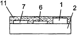
图2显示了包括氧化的硅晶片制成的基底(2)的本发明的伪参比电极(1),在基底上通过溅射直接沉积了单层的银薄膜(3),所述银薄膜厚度在100nm-1500nm之间,银薄膜(3)的厚度优选为1000nm。Figure 2 shows a pseudo-reference electrode (1) of the invention comprising a substrate (2) made of an oxidized silicon wafer, on which a single-layer silver film (3) has been directly deposited by sputtering, said silver film The thickness is between 100nm-1500nm, and the thickness of the silver thin film (3) is preferably 1000nm.
图2A是伪参比电极(1)的实施例,其中为了提高由氧化的硅晶片形成的基底(2)与银薄膜(3)之间的附着作用,提供了粘合材料层(4),优选为铬层,装置的操作特点并不因加入了该层而改变。Figure 2A is an embodiment of a pseudo-reference electrode (1), wherein in order to improve the adhesion between the substrate (2) formed by an oxidized silicon wafer and the silver film (3), a layer of adhesive material (4) is provided, A layer of chromium is preferred, the operating characteristics of the device are not altered by the addition of this layer.
用于制备伪参比电极(1)的方法是基于直接沉积单层的银薄膜(3)于基底(2)上,基底由氧化的硅、氧化铝或玻璃晶片形成,为了实现该目的使用了已知的溅射技术。The method used for the preparation of the pseudo-reference electrode (1) is based on the direct deposition of a single-layer silver film (3) on a substrate (2) formed from oxidized silicon, aluminum oxide or glass wafers, for this purpose using Known sputtering techniques.
图3显示了直接结合了本发明的伪参比电极(1)的电化学生物传感器(5),因此电化学生物传感器(5)包括由RF溅射沉积得到的厚度100nm,直径350微米的金盘形成的工作电极(6),由DC溅射沉积得到的厚度200nm的铂半圆形成的对电极(7)或辅助电极,和伪参比电极(1),所述伪参比电极是由DC溅射得到的厚度在100nm-1500nm之间,优选为1000nm的银半圆形成。Figure 3 shows an electrochemical biosensor (5) directly incorporating the pseudo-reference electrode (1) of the present invention, thus the electrochemical biosensor (5) comprises 100 nm thick gold with a diameter of 350 microns deposited by RF sputtering The working electrode (6) formed by the disk, the counter electrode (7) or the auxiliary electrode formed by the platinum semicircle with a thickness of 200nm obtained by DC sputtering deposition, and the pseudo reference electrode (1), the pseudo reference electrode is formed by DC The thickness obtained by sputtering is between 100nm-1500nm, preferably 1000nm silver semicircle.
金、铂和银,分别为工作电极(6)、对电极(7)和伪参比电极(1)的组成材料,均直接沉积于氧化的硅晶片形成的基底(2)上;在金膜、铂膜、银膜和氧化的硅晶片各个之间同样提供设置了粘合材料层(4),例如铬。Gold, platinum and silver, which are respectively the constituent materials of the working electrode (6), the counter electrode (7) and the pseudo-reference electrode (1), are all directly deposited on the substrate (2) formed by the oxidized silicon wafer; on the gold film An adhesive material layer (4), such as chromium, is also provided between each of the , platinum film, silver film and oxidized silicon wafer.
图4A至4J显示了制备电化学生物传感器(5)的过程,其中使用的技术(溅射、光刻法和PECVD(等离子体增强化学气相沉积))是硅芯片工业生产中的常见技术。光刻法过程使用树脂(8),像溅射和PECVD(等离子体化学气相沉积),对本领域技术人员来说是常规和公知的,因此不对其工艺进行描述。Figures 4A to 4J show the process of fabricating an electrochemical biosensor (5), where the techniques used (sputtering, photolithography and PECVD (Plasma Enhanced Chemical Vapor Deposition)) are common in the industrial production of silicon chips. Photolithographic processes using resins (8), like sputtering and PECVD (Plasma Chemical Vapor Deposition), are conventional and well known to those skilled in the art, so their processes will not be described.
因此首先在由氧化的硅晶片形成的基底(2)(图4A)上采用光刻过程限定对电极(7)、衬垫(7.1、6.1、1.1)和导轨(7.2、6.2、1.2)的几何形状,如图3所示,随后通过DC溅射沉积铂膜(9)(图4B和4C),和树脂(8),并且树脂(8)和沉积在树脂(8)上的材料通过剥离工艺移除,从而得到了对电极(7),衬垫(7.1、6.1、1.1)和导轨(7.2、6.2、1.2)。The geometry of the counter electrode (7), pads (7.1, 6.1, 1.1) and rails (7.2, 6.2, 1.2) is therefore first defined using a photolithographic process on a substrate (2) (Fig. 4A) formed from an oxidized silicon wafer. shape, as shown in Figure 3, followed by deposition of a platinum film (9) by DC sputtering (Figures 4B and 4C), and a resin (8), and the resin (8) and the material deposited on the resin (8) were passed through a lift-off process Removal, resulting in counter electrode (7), pads (7.1, 6.1, 1.1) and rails (7.2, 6.2, 1.2).
同样,随后通过另一光刻过程限定工作电极(6)的几何形状,通过RF溅射沉积金膜(10),通过进行剥离工艺以移除树脂(8)和沉积在其上的金(图4D和4E)。Likewise, the geometry of the working electrode (6) is then defined by another photolithographic process, the gold film (10) is deposited by RF sputtering, and the resin (8) and gold deposited thereon are removed by performing a lift-off process (Fig. 4D and 4E).
接着,通过又一光刻过程限定伪参比电极(1)的几何形状,通过DC溅射技术沉积银薄膜(3),树脂(8)和沉积在其上的材料通过剥离工艺移除(图4F和4G)。Next, the geometry of the pseudo-reference electrode (1) is defined by yet another photolithographic process, a thin film of silver (3) is deposited by DC sputtering technique, and the resin (8) and the material deposited thereon are removed by a lift-off process (Fig. 4F and 4G).
在所有沉积中可使用铬中间层以提高沉积膜(3,9,10)和基底各个之间的附着作用。A chromium interlayer can be used in all depositions to improve the adhesion between the deposited film (3, 9, 10) and each of the substrates.
最后,为了使生物传感器的非反应区域钝化,在工作电极(6)、对电极(7)和伪参比电极(1)中经化学蚀刻通过PECVD沉积二氧化硅层(11)。其余部分用光阻树脂(8)在刻蚀中得到保护,该光树脂(8)在先前已经通过光刻过程沉积并在化学蚀刻后通过剥离工艺移除(图4H,4I和4J)。Finally, in order to passivate the non-reactive areas of the biosensor, a silicon dioxide layer (11) is deposited by PECVD via chemical etching in the working electrode (6), counter electrode (7) and pseudo-reference electrode (1). The remainder is protected in the etch with a photoresist (8) that has previously been deposited by a photolithographic process and removed by a lift-off process after chemical etching (Figures 4H, 4I and 4J).
通过比较微型器件,即结合了本发明的伪参比电极(下文中称为TFRE)的电化学生物传感器,和配备了商业化的较大尺寸Ag/AgCl参比电极的电化学生物传感器,得到的结果如下所示。所有的实验在室温下的干净空间中进行。By comparing microdevices, namely electrochemical biosensors incorporating the pseudo-reference electrode (hereinafter referred to as TFRE) of the present invention, and electrochemical biosensors equipped with a commercially available larger-sized Ag/AgCl reference electrode, the obtained The results are shown below. All experiments were performed in a clean room at room temperature.
使用了银TFRE和商业化的Ag/AgCl参比电极的先进的微型器件在25mM的亚铁氰化钾(K3Fe(CN)6)溶液中表征。得到的结果如图5所示,其中可以看出对于通过用先进的TERE(X)测量六个微型器件的平均值得到的循环伏安图,和商业化的Ag/AgCl参比电极(Y)的循环伏安图,具有几乎相同的形状,显示了对应于铁氰化钾/亚铁氰化钾氧化还原偶的明确的氧化-还原行为。Advanced microdevices using silver TFREs and a commercial Ag/AgCl reference electrode were characterized in 25 mM potassium ferrocyanide (K3Fe(CN)6) solution. The obtained results are shown in Fig. 5, where it can be seen that for the cyclic voltammogram obtained by measuring the average value of six microdevices with the advanced TERE (X), and the commercial Ag/AgCl reference electrode (Y) The cyclic voltammograms of , with nearly identical shapes, show a well-defined oxidation–reduction behavior corresponding to the potassium ferricyanide/potassium ferrocyanide redox couple.
这两种情况下的的峰电流强度几乎相同:The peak current intensities are almost the same in both cases:
IpaAgTFRE=5.83±0.33μA;I paAgTFRE = 5.83 ± 0.33 μA;
IpaAg/AgClRE=5.80±0.39μA; IpaAg/AgClRE = 5.80±0.39μA;
(6个电极的平均值和标准方差);(mean and standard deviation of 6 electrodes);
峰电位之间有81mV的差异:There is an 81mV difference between the peak potentials:
EpaAgTERE=205±3mV;Epa AgTERE = 205±3mV;
EpaAg/AgClRE=286±1mV;EpaAg /AgClRE = 286±1mV;
(6个电极的平均值和标准方差)。(Mean and standard deviation of 6 electrodes).
两种参比电极获得非常接近的峰电流值的事实表明使用商业化Ag/AgCl参比电极或先进的银TFRE电极时,微型器件的灵敏度是相同的。The fact that very close peak current values were obtained for both reference electrodes indicates that the sensitivity of the micro-devices is the same when using a commercial Ag/AgCl reference electrode or an advanced silver TFRE electrode.
此外所研究的微型器件还显示出良好的重现性。使用了银TFRE电极的该器件得到的循环伏安图几乎是相同的,显示了分别在5.44至6.40μA和201至208mV范围内峰电流值和峰电位值几乎是相同的。In addition, the microdevices studied also showed good reproducibility. The cyclic voltammograms obtained for the device using silver TFRE electrodes are almost identical, showing almost identical peak current and peak potential values in the range of 5.44 to 6.40 μA and 201 to 208 mV, respectively.
IpaAgTFRE=5.83±0.33μA;I paAgTFRE = 5.83 ± 0.33 μA;
EpaAgTFRE=205±3mV,n=6;Epa AgTFRE = 205 ± 3mV, n = 6;
这些电位差异可能归因于溅射过程中银层的厚度在晶片的一侧到另一侧会有1微米至850nm范围的变化。These potential differences may be attributed to the thickness of the silver layer varying from one side of the wafer to the other during sputtering in the range of 1 micron to 850 nm.
众所周知,参比电极的主要问题之一是其电位的经时稳定性。为测试先进的银TFRE电极的稳定性,对其电化学性能进行了超过一个月的研究。It is well known that one of the main problems of reference electrodes is the stability of their potential over time. To test the stability of the advanced silver TFRE electrode, its electrochemical performance was investigated for more than one month.
在这段时间里,每两天一次周期性地校验从循环伏安曲线得到的阳极/阴极峰电位和峰电流。每次测量后,电极均用超纯水(Milli QTM water)冲洗,用氮气流吹干并存放在无氮的氧气氛中(99.99%)。During this period, the anodic/cathodic peak potentials and peak currents obtained from the cyclic voltammetry curves were checked periodically every two days. After each measurement, the electrodes were rinsed with ultrapure water (Milli Q ™ water), blown dry with nitrogen flow and stored in a nitrogen-free oxygen atmosphere (99.99%).
图6显示了5个微型器件在这段时间内测量的平均值和标准方差;峰电流强度(Ipa)以点状线表示,而电位(Epa)以实线表示。可以看出,在取样期间得到的响应基本上保持线性:Figure 6 shows the mean and standard deviation measured over this period for five microdevices; the peak current intensity (I pa ) is shown as a dotted line, while the potential (Epa) is shown as a solid line. It can be seen that the resulting response remains essentially linear during sampling:
Epa=208±6mV,Ipa=5.7±0.20μA;Epa=208±6mV, Ipa =5.7±0.20μA;
(5个微型器件的平均值和标准方差)。(Mean and standard deviation of 5 microdevices).
所得的峰电位值和峰电流值的不同(在同一天)归因于在研究中使用的不同传感器,这些传感器如上所述的,因溅射过程不会完全相同。The resulting differences in peak potential and peak current values (on the same day) were attributed to the different sensors used in the study which, as mentioned above, would not be identical due to the sputtering process.
下面的表显示了电位值的平均值(Epa),峰电流值的平均值(Ipa)以及得到的各个电极的峰电位值和峰电流值的最大差值。在最坏的例子(芯片4和5)中峰电位和峰电流的最大差值分别为14mV和0.80μA,而在最好的例子中,则分别是5mV和0.31μA(芯片3)。The table below shows the average value of the potential value (Epa), the average value of the peak current value ( Ipa ) and the maximum difference between the peak potential value and the peak current value obtained for each electrode. The maximum difference in peak potential and peak current is 14mV and 0.80μA in the worst case (
还未有关于通过溅射技术制备的TFREs的长期稳定性报道。无论如何,根据在前的结果可以得出的结论是提议的伪参比电极是经时稳定的。The long-term stability of TFREs prepared by sputtering technique has not been reported yet. Regardless, it can be concluded from the previous results that the proposed pseudo-reference electrode is stable over time.
Claims (6)
Applications Claiming Priority (3)
| Application Number | Priority Date | Filing Date | Title |
|---|---|---|---|
| ES200902118A ES2358938B1 (en) | 2009-11-05 | 2009-11-05 | PSEUDO-ELECTRODE OF REFERENCE OF SLIM FILM AND PROCEDURE FOR ITS MANUFACTURE. |
| ESP200902118 | 2009-11-05 | ||
| PCT/ES2010/000418 WO2011054982A1 (en) | 2009-11-05 | 2010-10-15 | Thin-film reference pseudo-electrode and method for the production thereof |
Publications (1)
| Publication Number | Publication Date |
|---|---|
| CN102639994A true CN102639994A (en) | 2012-08-15 |
Family
ID=43920176
Family Applications (1)
| Application Number | Title | Priority Date | Filing Date |
|---|---|---|---|
| CN2010800497921A Pending CN102639994A (en) | 2009-11-05 | 2010-10-15 | Thin-film reference pseudo-electrode and method for the production thereof |
Country Status (6)
| Country | Link |
|---|---|
| US (1) | US20120211363A1 (en) |
| EP (1) | EP2498082A4 (en) |
| CN (1) | CN102639994A (en) |
| BR (1) | BR112012010367A2 (en) |
| ES (1) | ES2358938B1 (en) |
| WO (1) | WO2011054982A1 (en) |
Cited By (1)
| Publication number | Priority date | Publication date | Assignee | Title |
|---|---|---|---|---|
| CN113109408A (en) * | 2021-04-08 | 2021-07-13 | 海南师范大学 | Portable palm electrochemical sensor for detecting enzyme concentration based on chip electrode and preparation method and detection method thereof |
Families Citing this family (3)
| Publication number | Priority date | Publication date | Assignee | Title |
|---|---|---|---|---|
| WO2016202722A1 (en) * | 2015-06-15 | 2016-12-22 | Roche Diagnostics Gmbh | Method and test element for electrochemically detecting at least one analyte in a sample of a body fluid |
| CN106018527B (en) * | 2016-05-17 | 2019-01-08 | 西安电子科技大学 | GaN biosensor and production method with integrated form solid film Pt reference electrode |
| JP7279260B2 (en) * | 2020-03-27 | 2023-05-22 | 子誠 朱 | Electrodes and electrode tips |
Citations (2)
| Publication number | Priority date | Publication date | Assignee | Title |
|---|---|---|---|---|
| JPH08260134A (en) * | 1995-03-22 | 1996-10-08 | Toppan Printing Co Ltd | Sputtering target |
| CN101216448A (en) * | 2008-01-09 | 2008-07-09 | 浙江大学 | Hydrogen sensor based on palladium-silver wire electrode |
Family Cites Families (5)
| Publication number | Priority date | Publication date | Assignee | Title |
|---|---|---|---|---|
| US4933048A (en) | 1988-02-16 | 1990-06-12 | I-Stat Corporation | Reference electrode, method of making and method of using same |
| AU3373297A (en) * | 1996-06-17 | 1998-01-07 | Mercury Diagnostics Inc. | Electrochemical test device and related methods |
| US5958791A (en) * | 1996-09-27 | 1999-09-28 | Innovative Biotechnologies, Inc. | Interdigitated electrode arrays for liposome-enhanced immunoassay and test device |
| JP2001004581A (en) * | 1999-06-24 | 2001-01-12 | Sentan Kagaku Gijutsu Incubation Center:Kk | Very small reference electrode |
| CN101216451B (en) | 2008-01-18 | 2012-01-04 | 华东理工大学 | DNA biosensor electrode manufacture method and uses thereof |
-
2009
- 2009-11-05 ES ES200902118A patent/ES2358938B1/en not_active Expired - Fee Related
-
2010
- 2010-10-15 WO PCT/ES2010/000418 patent/WO2011054982A1/en active Application Filing
- 2010-10-15 CN CN2010800497921A patent/CN102639994A/en active Pending
- 2010-10-15 US US13/504,999 patent/US20120211363A1/en not_active Abandoned
- 2010-10-15 BR BR112012010367A patent/BR112012010367A2/en not_active IP Right Cessation
- 2010-10-15 EP EP10827937.3A patent/EP2498082A4/en not_active Withdrawn
Patent Citations (2)
| Publication number | Priority date | Publication date | Assignee | Title |
|---|---|---|---|---|
| JPH08260134A (en) * | 1995-03-22 | 1996-10-08 | Toppan Printing Co Ltd | Sputtering target |
| CN101216448A (en) * | 2008-01-09 | 2008-07-09 | 浙江大学 | Hydrogen sensor based on palladium-silver wire electrode |
Non-Patent Citations (7)
Cited By (1)
| Publication number | Priority date | Publication date | Assignee | Title |
|---|---|---|---|---|
| CN113109408A (en) * | 2021-04-08 | 2021-07-13 | 海南师范大学 | Portable palm electrochemical sensor for detecting enzyme concentration based on chip electrode and preparation method and detection method thereof |
Also Published As
| Publication number | Publication date |
|---|---|
| EP2498082A4 (en) | 2014-12-31 |
| WO2011054982A1 (en) | 2011-05-12 |
| US20120211363A1 (en) | 2012-08-23 |
| ES2358938B1 (en) | 2011-12-30 |
| ES2358938A1 (en) | 2011-05-17 |
| BR112012010367A2 (en) | 2017-07-04 |
| EP2498082A1 (en) | 2012-09-12 |
Similar Documents
| Publication | Publication Date | Title |
|---|---|---|
| CN101595381B (en) | Electrode plate for electrochemical measurement, electrochemical measuring apparatus having the electrode plate, and method for determining target substance by using the electrode plate | |
| TWI422818B (en) | Hydrogen ion sensing field effect transistor and manufacturing method thereof | |
| US20100084267A1 (en) | Pair of measuring electrodes, biosensor comprising a pair of measuring electrodes of this type, and production process | |
| WO2009144869A1 (en) | Method for detecting or quantitating target substance by using electrochemical measurement device, electrochemical measurement device, and electrode plate for electrochemical measurement | |
| CN104280365A (en) | Dual-detection biosensing chip and preparation method thereof and DNA detection method | |
| Phokharatkul et al. | AAO–CNTs electrode on microfluidic flow injection system for rapid iodide sensing | |
| CN102639994A (en) | Thin-film reference pseudo-electrode and method for the production thereof | |
| CN105954333A (en) | Gold nanobelt three-electrode sensor used for monitoring heavy metal and preparation method thereof | |
| Chou et al. | Fabrication and application of ruthenium-doped titanium dioxide films as electrode material for ion-sensitive extended-gate FETs | |
| Mello et al. | Well-established materials in microelectronic devices systems for differential-mode extended-gate field effect transistor chemical sensors | |
| Hayasaka et al. | Integration of boron-doped diamond microelectrode on CMOS-based amperometric sensor array by film transfer technology | |
| Gardner et al. | Development of a microelectrode array sensing platform for combination electrochemical and spectrochemical aqueous ion testing | |
| KR20120126977A (en) | CNT-based three electrode system, fabrication of the same and electrochemical biosensor using the same | |
| CN1288436C (en) | Preparation method of reference electrode compatible with micro electromechanical system technology | |
| CN112268942A (en) | Micro-nano sensing device, preparation method thereof and pH value detection method | |
| CN101627301A (en) | Electrode plate for electrochemical measurement, electrochemical measuring instrument having the electrode plate for electrochemical measurement, and method for determining target substance using the | |
| CN118032873A (en) | A hydrogen sulfide gas sensor and its preparation process | |
| CN1749745A (en) | Electric heating double parameter detecting chip and preparation method thereof | |
| Wang et al. | Research on a miniature multiparameter water quality sensor chip and a system with a temperature compensation function | |
| Chou et al. | Development of a disposable all-solid-state ascorbic acid biosensor and miniaturized reference electrode fabricated on single substrate | |
| CN114660157A (en) | An extended structure field effect transistor | |
| Schöning et al. | A silicon-based microelectrode array for chemical analysis | |
| Iken et al. | Novel thin-film polymeric materials for the detection of heavy metals | |
| JPH03246460A (en) | Electrochemical detector | |
| Schöning et al. | Iodide ion-sensitive field-effect structures |
Legal Events
| Date | Code | Title | Description |
|---|---|---|---|
| C06 | Publication | ||
| PB01 | Publication | ||
| C10 | Entry into substantive examination | ||
| SE01 | Entry into force of request for substantive examination | ||
| C02 | Deemed withdrawal of patent application after publication (patent law 2001) | ||
| WD01 | Invention patent application deemed withdrawn after publication |
Application publication date: 20120815 |