CN102629593B - Flexible electronic device and manufacturing method thereof - Google Patents
Flexible electronic device and manufacturing method thereof Download PDFInfo
- Publication number
- CN102629593B CN102629593B CN201210092783.1A CN201210092783A CN102629593B CN 102629593 B CN102629593 B CN 102629593B CN 201210092783 A CN201210092783 A CN 201210092783A CN 102629593 B CN102629593 B CN 102629593B
- Authority
- CN
- China
- Prior art keywords
- area
- layer
- region
- base material
- polyimide
- Prior art date
- Legal status (The legal status is an assumption and is not a legal conclusion. Google has not performed a legal analysis and makes no representation as to the accuracy of the status listed.)
- Active
Links
- 238000004519 manufacturing process Methods 0.000 title claims abstract description 20
- 239000000463 material Substances 0.000 claims description 57
- 239000004642 Polyimide Substances 0.000 claims description 54
- 229920001721 polyimide Polymers 0.000 claims description 54
- 238000000034 method Methods 0.000 claims description 38
- 229920005575 poly(amic acid) Polymers 0.000 claims description 28
- 238000000576 coating method Methods 0.000 claims description 22
- 239000011248 coating agent Substances 0.000 claims description 20
- 230000001737 promoting effect Effects 0.000 claims description 16
- 238000000059 patterning Methods 0.000 claims description 7
- QVGXLLKOCUKJST-UHFFFAOYSA-N atomic oxygen Chemical compound [O] QVGXLLKOCUKJST-UHFFFAOYSA-N 0.000 claims description 3
- 238000005530 etching Methods 0.000 claims description 3
- 229910044991 metal oxide Inorganic materials 0.000 claims description 3
- 150000004706 metal oxides Chemical class 0.000 claims description 3
- 239000001301 oxygen Substances 0.000 claims description 3
- 229910052760 oxygen Inorganic materials 0.000 claims description 3
- 239000010410 layer Substances 0.000 claims 33
- 238000009434 installation Methods 0.000 claims 8
- 239000000853 adhesive Substances 0.000 claims 4
- 230000001070 adhesive effect Effects 0.000 claims 4
- 239000011247 coating layer Substances 0.000 claims 2
- 239000007789 gas Substances 0.000 claims 2
- 238000009281 ultraviolet germicidal irradiation Methods 0.000 claims 2
- MRNHPUHPBOKKQT-UHFFFAOYSA-N indium;tin;hydrate Chemical compound O.[In].[Sn] MRNHPUHPBOKKQT-UHFFFAOYSA-N 0.000 claims 1
- 230000001678 irradiating effect Effects 0.000 claims 1
- 238000010023 transfer printing Methods 0.000 claims 1
- 239000000758 substrate Substances 0.000 abstract description 104
- 238000005520 cutting process Methods 0.000 abstract description 9
- 239000004033 plastic Substances 0.000 description 31
- 239000011521 glass Substances 0.000 description 10
- 150000001282 organosilanes Chemical class 0.000 description 8
- 229920002120 photoresistant polymer Polymers 0.000 description 5
- 239000012808 vapor phase Substances 0.000 description 4
- 239000002253 acid Substances 0.000 description 3
- 239000000919 ceramic Substances 0.000 description 3
- 238000010586 diagram Methods 0.000 description 3
- 239000002184 metal Substances 0.000 description 3
- 229910052751 metal Inorganic materials 0.000 description 3
- 238000005240 physical vapour deposition Methods 0.000 description 3
- 239000010453 quartz Substances 0.000 description 3
- VYPSYNLAJGMNEJ-UHFFFAOYSA-N silicon dioxide Inorganic materials O=[Si]=O VYPSYNLAJGMNEJ-UHFFFAOYSA-N 0.000 description 3
- BLRPTPMANUNPDV-UHFFFAOYSA-N Silane Chemical compound [SiH4] BLRPTPMANUNPDV-UHFFFAOYSA-N 0.000 description 2
- 238000005229 chemical vapour deposition Methods 0.000 description 2
- 229910000077 silane Inorganic materials 0.000 description 2
- 238000004544 sputter deposition Methods 0.000 description 2
- 239000010409 thin film Substances 0.000 description 2
- 239000004952 Polyamide Substances 0.000 description 1
- 150000001408 amides Chemical class 0.000 description 1
- 230000007812 deficiency Effects 0.000 description 1
- 238000005137 deposition process Methods 0.000 description 1
- 239000010408 film Substances 0.000 description 1
- 239000005357 flat glass Substances 0.000 description 1
- 150000003949 imides Chemical class 0.000 description 1
- GRPQBOKWXNIQMF-UHFFFAOYSA-N indium(3+) oxygen(2-) tin(4+) Chemical compound [Sn+4].[O-2].[In+3] GRPQBOKWXNIQMF-UHFFFAOYSA-N 0.000 description 1
- AMGQUBHHOARCQH-UHFFFAOYSA-N indium;oxotin Chemical compound [In].[Sn]=O AMGQUBHHOARCQH-UHFFFAOYSA-N 0.000 description 1
- 239000000203 mixture Substances 0.000 description 1
- 238000012986 modification Methods 0.000 description 1
- 230000004048 modification Effects 0.000 description 1
- 238000000206 photolithography Methods 0.000 description 1
- 229920002647 polyamide Polymers 0.000 description 1
Images


Classifications
-
- H—ELECTRICITY
- H10—SEMICONDUCTOR DEVICES; ELECTRIC SOLID-STATE DEVICES NOT OTHERWISE PROVIDED FOR
- H10D—INORGANIC ELECTRIC SEMICONDUCTOR DEVICES
- H10D86/00—Integrated devices formed in or on insulating or conducting substrates, e.g. formed in silicon-on-insulator [SOI] substrates or on stainless steel or glass substrates
- H10D86/01—Manufacture or treatment
- H10D86/021—Manufacture or treatment of multiple TFTs
- H10D86/0214—Manufacture or treatment of multiple TFTs using temporary substrates
-
- Y—GENERAL TAGGING OF NEW TECHNOLOGICAL DEVELOPMENTS; GENERAL TAGGING OF CROSS-SECTIONAL TECHNOLOGIES SPANNING OVER SEVERAL SECTIONS OF THE IPC; TECHNICAL SUBJECTS COVERED BY FORMER USPC CROSS-REFERENCE ART COLLECTIONS [XRACs] AND DIGESTS
- Y10—TECHNICAL SUBJECTS COVERED BY FORMER USPC
- Y10T—TECHNICAL SUBJECTS COVERED BY FORMER US CLASSIFICATION
- Y10T29/00—Metal working
- Y10T29/49—Method of mechanical manufacture
- Y10T29/49002—Electrical device making
- Y10T29/49117—Conductor or circuit manufacturing
- Y10T29/49124—On flat or curved insulated base, e.g., printed circuit, etc.
- Y10T29/4913—Assembling to base an electrical component, e.g., capacitor, etc.
-
- Y—GENERAL TAGGING OF NEW TECHNOLOGICAL DEVELOPMENTS; GENERAL TAGGING OF CROSS-SECTIONAL TECHNOLOGIES SPANNING OVER SEVERAL SECTIONS OF THE IPC; TECHNICAL SUBJECTS COVERED BY FORMER USPC CROSS-REFERENCE ART COLLECTIONS [XRACs] AND DIGESTS
- Y10—TECHNICAL SUBJECTS COVERED BY FORMER USPC
- Y10T—TECHNICAL SUBJECTS COVERED BY FORMER US CLASSIFICATION
- Y10T428/00—Stock material or miscellaneous articles
- Y10T428/24—Structurally defined web or sheet [e.g., overall dimension, etc.]
- Y10T428/24479—Structurally defined web or sheet [e.g., overall dimension, etc.] including variation in thickness
Landscapes
- Electroluminescent Light Sources (AREA)
- Laminated Bodies (AREA)
- Thin Film Transistor (AREA)
Abstract
Description
技术领域 technical field
本发明涉及一种软性电子装置,特别是有关于一种软性电子装置的制作方法。The invention relates to a flexible electronic device, in particular to a manufacturing method of a flexible electronic device.
背景技术 Background technique
有两种方法主要用以制造软性显示器:卷对卷(roll to roll)以及贴附软性基材至玻璃基材。对于后者的方法,已证明从玻璃基材分离软性基材以便完成软性显示器的制造过程为一艰巨的事。一种公知离型方法将牺牲层插入软性基材与玻璃基材之间,其中牺牲层的材料为氧化物,此氧化物可吸收某些波长的激光的能量。借着激光扫掠玻璃基材的背面,氧化层吸收穿透玻璃基材的激光能量,如此一来软性基材与玻璃基材分离。然而,激光的使用增加成本且对电子零件造成损伤。There are two main methods used to manufacture flexible displays: roll to roll and attaching a flexible substrate to a glass substrate. For the latter approach, separating the flexible substrate from the glass substrate in order to complete the fabrication process of the flexible display has proven to be a difficult task. A known release method inserts a sacrificial layer between a flexible substrate and a glass substrate, wherein the material of the sacrificial layer is an oxide, which can absorb laser energy of certain wavelengths. By scanning the backside of the glass substrate with a laser, the oxide layer absorbs the laser energy that penetrates the glass substrate, so that the soft substrate is separated from the glass substrate. However, the use of lasers increases cost and causes damage to electronic parts.
另一方法设置一有机离型层于软性基材与玻璃基材之间。然而,在制造有机离型层的期间可能形成小岛结构,此些小岛结构可能造成孔洞形成于软性基材中、以及软性基材的非均匀厚度。Another method provides an organic release layer between the flexible substrate and the glass substrate. However, island structures may be formed during the manufacture of the organic release layer, and these island structures may cause holes to be formed in the flexible substrate and non-uniform thickness of the flexible substrate.
因此,在此领域中,存在一个至今仍未提出的需求,以对付上述缺陷与不足。Therefore, there exists a hitherto unaddressed need in this field to address the aforementioned deficiencies and inadequacies.
发明内容 Contents of the invention
在本发明的一态样中,一种软性电子装置的制作方法,包含:提供基材;形成第一层于基材上,以在基材中定义出第一区域与第二区域,第二区域围绕第一区域,以至少局部地暴露出第一区域中的基材,且第一层至少部分位于第二区域中;形成第二层于第一区域与第二区域上方的第一层上,因而第二层与第一区域中的基材间的附着力较第二层与第二区域中的第一层间的附着力弱;形成电子装置层于第一区域上方的第二层上,其中电子装置层在第一区域上定义出边界,且此边界投影地位于第一区域中;以及通过沿着轮廓切穿第二层的方式,将电子装置层和部分的第二层与基材分离,此轮廓相等于或大于电子装置层的边界,但不超出第一区域。In one aspect of the present invention, a method for manufacturing a flexible electronic device includes: providing a substrate; forming a first layer on the substrate to define a first region and a second region in the substrate, the second Two regions surround the first region to at least partially expose the substrate in the first region, and the first layer is at least partially located in the second region; forming a second layer on the first region and the first layer above the second region on, thus the adhesion between the second layer and the substrate in the first region is weaker than the adhesion between the second layer and the first layer in the second region; forming the second layer of the electronic device layer above the first region , wherein the electronics layer defines a boundary on and projectively in the first region; and the electronics layer and part of the second layer are aligned with the second layer by cutting through the second layer along the contour The substrate is separated, and the outline is equal to or greater than the boundary of the electronic device layer, but does not exceed the first region.
在本发明的另一态样中,一种软性电子装置的制作方法,包含:提供基材,此基材具有第一表面与相对的第二表面;涂布第一聚酰胺酸(Polyamic Acid;PAA)在基材的第一表面上,以形成第一聚亚酰胺(Polyimide)层,借以在基材中定义出第一区域与第二区域,其中第一聚亚酰胺层形成在第一区域上,且第二区域围绕第一区域;涂布第二聚酰胺酸于基材的第一区域中的第一聚亚酰胺层与基材的第二区域上,以形成第二聚亚酰胺层在第一聚亚酰胺层与第二区域上,其中第二聚酰胺酸以有机硅烷合成,如此第一聚亚酰胺层与第一区域中的基材间的附着力较第二聚亚酰胺层与第二区域中的基材间的附着力弱;形成电子装置层于第一区域上方的第二聚亚酰胺层上,其中电子装置层于第一区域上定义出边界,且此边界投影地位于第一区域中;以及通过沿着轮廓切穿第二聚亚酰胺层与第一聚亚酰胺层的方式,将电子装置层、部分的第二聚亚酰胺层和部分的第一聚亚酰胺层与基材分离,此轮廓相等于或大于电子装置层的边界,但不超出第一区域。In another aspect of the present invention, a method of manufacturing a flexible electronic device includes: providing a substrate, the substrate has a first surface and an opposite second surface; coating a first polyamic acid (Polyamic Acid ; PAA) on the first surface of the substrate to form a first polyimide (Polyimide) layer, thereby defining a first region and a second region in the substrate, wherein the first polyimide layer is formed on the first area, and the second area surrounds the first area; coating the second polyamic acid on the first polyimide layer in the first area of the substrate and on the second area of the substrate to form a second polyimide The layer is on the first polyimide layer and the second area, wherein the second polyamic acid is synthesized with organosilane, so that the adhesion between the first polyimide layer and the substrate in the first area is better than that of the second polyimide The adhesion between the layer and the substrate in the second region is weak; the electronic device layer is formed on the second polyimide layer above the first region, wherein the electronic device layer defines a boundary on the first region, and the boundary projects located in the first region; and by cutting through the second polyimide layer and the first polyimide layer along the contour, the electronic device layer, part of the second polyimide layer and part of the first polyimide layer The amide layer is separated from the substrate with a profile equal to or greater than the boundary of the electronic device layer, but not beyond the first region.
在本发明的又一态样中,本发明关于一种依照以上所公开的方法所制作的软性电子装置。In yet another aspect of the present invention, the present invention relates to a flexible electronic device manufactured according to the method disclosed above.
本发明的这些与其他态样从结合下列附图所做的较佳实施例的描述中将变得更明显,然而在不偏离本发明公开的新观念的精神与范围下,可变更其中的变化与变异。These and other aspects of the present invention will become more apparent from the description of the preferred embodiments in conjunction with the following drawings, however changes may be made without departing from the spirit and scope of the novel concepts disclosed in the present invention with variation.
附图说明 Description of drawings
所附附图绘示出本发明的一或多个实施例,连同所载描述,用以解释本发明的原理。只要有可能,相同参考符号应用于整个附图中,以表示一实施例的相同或相似元件,其中:The accompanying drawings illustrate one or more embodiments of the invention and together with the description serve to explain the principles of the invention. Wherever possible, the same reference signs are used throughout the drawings to represent the same or like elements of an embodiment, in which:
图1A至图1G图绘示根据本发明的一实施例的一种软性电子装置的制作工艺的示意图;1A to 1G are schematic diagrams illustrating a manufacturing process of a flexible electronic device according to an embodiment of the present invention;
图2A至图2H绘示根据本发明的另一实施例的一种软性电子装置的制作工艺的示意图;以及2A to 2H are schematic diagrams illustrating a manufacturing process of a flexible electronic device according to another embodiment of the present invention; and
图3A至图3H绘示根据本发明的又一实施例的一种软性电子装置的制作工艺的示意图。3A to 3H are schematic diagrams illustrating a manufacturing process of a flexible electronic device according to yet another embodiment of the present invention.
其中,附图标记Among them, reference signs
110:基材 111:第一区域110: Substrate 111: The first area
112:第一表面 113:第二区域112: First Surface 113: Second Area
114:第二表面 120:助粘层114: Second surface 120: Adhesion-promoting layer
126:掩膜 128:紫外光126: mask 128: ultraviolet light
130:塑胶层 140:电子装置层130: Plastic layer 140: Electronic device layer
142:边界 210:基材142: Boundary 210: Substrate
211:第一区域 212:上表面211: First area 212: Upper surface
213:第二区域 214:第二表面213: Second area 214: Second surface
220:抗剥离层 222:图案220: Anti-peeling layer 222: Pattern
224:图案 226:光阻224: pattern 226: photoresist
228:等离子 230:塑胶层228: Plasma 230: Plastic layer
240:电子装置层 242:边界240: Electronic device layer 242: Boundary
310:基材 311:第一区域310: Substrate 311: The first area
311A:轮廓 312:上表面311A: outline 312: upper surface
313:第二区域 314:第二表面313: Second area 314: Second surface
320:第一聚亚酰胺层 322:上表面320: first polyimide layer 322: upper surface
330:第二聚亚酰胺层 340:电子装置层330: second polyimide layer 340: electronic device layer
342:边界342: Boundary
具体实施方式 Detailed ways
以下将参考附图而更充分地描述本发明,其中附图绘示出本发明的示范实施例。然而,本发明可以许多不同形式加以体现,且不应理解为限制于此所提出的实施例。相反地,由于此些实施例的提供,因而此公开可对本领域技术人员彻底、完全且完整表达本发明的范围。相同的参考数字在各处代表相同的元件。The present invention will be described more fully hereinafter with reference to the accompanying drawings, in which exemplary embodiments of the invention are shown. This invention may, however, be embodied in many different forms and should not be construed as limited to the embodiments set forth herein. Rather, it is that these embodiments are provided so that this disclosure will be thorough, complete and fully convey the scope of the invention to those skilled in the art. The same reference numerals represent the same elements throughout.
可理解的是当称一元件位于另一元件“上(on)”时,其可为直接位于其他元件上、或介于中间的元件可出现在其间。相反地,当称一元件直接位于另一元件“上(directly on)”时,并无介于中间的元件出现。如于此所使用,用语(terms)“和/或(and/or)”包含一个或多个相关的列出项目的任一与所有组合。It will be understood that when an element is referred to as being "on" another element, it can be directly on the other element or intervening elements may be present therebetween. In contrast, when an element is referred to as being "directly on" another element, no intervening elements are present. As used herein, the terms "and/or" include any and all combinations of one or more of the associated listed items.
可理解的是,虽然在此可使用用语第一(first),第二(second)与第三(third)等来描述各种元件、零件、区域、层和/或部分,但此些用语不应限制此些元件、零件、区域、层和/或部分。此些用语仅用以区别一元件、零件、区域、层和/或部分与另一元件、零件、区域、层和/或部分。因此,可在不偏离本发明的教示的情况下,将以下讨论的第一元件、零件、区域、层和/或部分称为第二元件、零件、区域、层和/或部分。It is to be understood that although the terms first, second and third, etc. may be used herein to describe various elements, parts, regions, layers and/or sections, these terms do not Such elements, parts, regions, layers and/or sections should be limited. These terms are only used to distinguish one element, component, region, layer and/or section from another element, component, region, layer and/or section. Thus, a first element, component, region, layer and/or section discussed below could be termed a second element, component, region, layer and/or section without departing from the teachings of the present invention.
在此使用的术语仅用于描述特定实施例的目的,并非用以限制本发明。如于此所使用,除非内容清楚指定,单数形式“一(a)”与“该(the)”亦欲包含多数形式。将进一步了解的是,用语“包含(comprises)”及/或“包含(comprising)”、或“包含(includes)”及/或“包含(including)”、或“具有(has)”及/或“具有(having)”应用在说明书中时,明确说明所述特征、区域、整体、步骤、操作、元素、及/或构件的存在,但并未排除一或更多其他特征、区域、整体、步骤、操作、元件、零件及/或其族群的存在或加入。The terminology used herein is for the purpose of describing particular embodiments only and is not intended to be limiting of the invention. As used herein, the singular forms "a" and "the" are intended to include the plural unless the content clearly dictates otherwise. It will be further understood that the terms "comprises" and/or "comprising", or "includes" and/or "including", or "has" and/or When "having (having)" is used in the description, it clearly states the existence of the features, regions, integers, steps, operations, elements, and/or components, but does not exclude one or more other features, regions, integers, The presence or addition of steps, operations, elements, parts and/or groups thereof.
此外,相对用语,例如:“下(lower)”或“底部(bottom)”和“上(upper)”或“顶部(top)”于此可用以描述如图中所绘示的一元件与另一元件的关系。可理解的是,除了图中所描绘的方位外,相对用语意欲包含元件的不同方位。例如:若图中的元件翻转,被描述为在此另一元件的“下”侧的元件接下来将位于此另一元件的“上”侧的方位。因此,例示性用语“下”根据图的特定方位可包含“下”和“上”的两方位。相同地,若图中的元件翻转,被描述为在另一元件“之下(below)”或“下方(beneath)”的元件则接下来将位于此另一元件的“上方(above)”的方位。因此,例示性用语“之下”或“下方”可包含上方及下方两方位。In addition, relative terms such as "lower" or "bottom" and "upper" or "top" may be used herein to describe the relationship between one element and another as shown in the figures. A component relationship. It will be understood that relative terms are intended to encompass different orientations of elements in addition to the orientation depicted in the figures. For example, if an element in the figures is turned over, elements described as being on the "lower" side of other elements would then be oriented on the "upper" side of the other elements. Thus, the exemplary term "lower" can encompass both an orientation of "lower" and "upper" depending on the particular orientation of the figures. Similarly, if an element in the figures is turned over, an element described as "below" or "beneath" another element would then be oriented "above" the other element. position. Thus, the exemplary terms "under" or "under" can encompass both an orientation of above and below.
除非特别定义,否则在此所使用的所有用语(包含科技与科学用语)具有相同于熟习本发明所属技术领域者所广为了解的意义。将可进一步了解的是,用语,例如以常用辞典定义的用语,应解释成具有与它们在相关领域和本公开的上下文中的意义一致的意义,且将不会以理想化或过度正式的意义来加以解读,除非在此这样特别定义。Unless otherwise defined, all terms (including technical and scientific terms) used herein have the same meaning as commonly understood by those skilled in the art to which this invention belongs. It will be further appreciated that terms, such as those defined in commonly used dictionaries, should be interpreted to have a meaning consistent with their meaning in the relevant art and in the context of this disclosure, and will not be interpreted in an idealized or overly formal sense to be interpreted unless otherwise specifically defined herein.
如在此所使用的用语“大约(around)”、“约(about)”或“近乎(approximately)”应大体上意味在给定值或范围的20%以内,较佳在10%以内,更佳在5%内。在此所提供的数量为近似的,因此意味着若无特别陈述,可以用语“大约”、“约”或“近乎”加以表示。As used herein, the terms "around", "about" or "approximately" shall generally mean within 20%, preferably within 10%, and more preferably within 10% of a given value or range Best within 5%. Quantities provided herein are approximate, thus meaning that the words "about", "approximately" or "approximately" may be used unless otherwise stated.
可了解如在此所使用的用语“包含(comprising)”、“包含(including)”、“具有(having)”、“含有(containing)”、“包含(involving)”等等,为开放性的(open-ended),即意指包含但不限于。It will be understood that the terms "comprising," "including," "having," "containing," "involving," etc., as used herein, are open-ended (open-ended), which means including but not limited to.
于此所使用的用语“层(layer)”指薄片或薄膜。As used herein, the term "layer" refers to a sheet or film.
关于本发明的实施例将结合附图图1A-图1G、图2A-图2H与图3A-图3H进行描述。依照本发明的目的,如同在此体现与概括描述的,在一态样中,本发明关于一种软性电子装置的制作方法。Embodiments of the present invention will be described with reference to FIGS. 1A-1G , 2A-2H and 3A-3H . In accordance with the purpose of the present invention, as embodied and broadly described herein, in one aspect, the present invention relates to a method of manufacturing a flexible electronic device.
现在请参考图1A-图1G,其绘示根据本发明的一实施例的一种软性电子装置的制作方法。此方法包含以下步骤:首先,提供基材110,基材110具有第一(平坦)表面112与相对的第二表面114。基材110可为玻璃、石英、塑胶、陶瓷、金属或其他类似材料的平坦基材。在一示范实施例中,基材110平坦的玻璃基材。Please refer now to FIG. 1A-FIG. 1G , which illustrate a manufacturing method of a flexible electronic device according to an embodiment of the present invention. The method includes the following steps: firstly, a
然后,以助粘材料形成助粘层120于基材110的第一表面112上,如图1B所示。在一例子中,助粘材料有机硅烷。可理解的是其他助粘材料亦可用以实施本发明。Then, an adhesion-promoting
在一实施例中,形成助粘层120时包含以下步骤:以含有有机硅烷的助粘材料涂布基材110的第一表面112,及在第一温度下烘烤涂布于基材110的有机硅烷第一段时间,以形成助粘层120于基材110上,如图1B所示。涂布工艺包含涂过量的有机硅烷溶液至平坦基材110的第一表面112,如图1A所示,然后在高转速下旋转有机硅烷溶液,以散开有机硅烷溶液,而形成涂布有有机硅烷的基材。在一实施例中,第一温度的范围介于约50℃至250℃,且第一段时间的范围介于约5分钟至10分钟。烘烤(第一)温度和时间较佳约120℃与约5分钟,或约200℃与约1分钟。In one embodiment, forming the adhesion-promoting
在另一实施例中,形成助粘层120时包含气相涂布助粘材料于基材110的第一表面112,以形成助粘层120,如图1B所示。气相涂布工艺可为物理气相沉积(Physical Vapor Deposition;PVD)工艺、化学气相沉积(Chemical VaporDeposition;CVD)工艺或其他类似的工艺。In another embodiment, the adhesion-promoting
此外,对助粘层120进行图案化工艺,以在基材110中定义出第一区域111与第二区域113,第二区域113围绕第一区域111。在一实施例中,图案化工艺包含转印具有对应于第一区域111与第二区域113的图案的掩膜126于助粘层120上,以及在空气或氧气的环境中,例如烘箱,以紫外(Ultraviolet;UV)光128处理助粘层120与基材110,如此UV光照射第一区域111上的助粘层120,而第二区域113上的助粘层120则被遮蔽而不受UV光照射,如图1C所示。在第二温度下进行图案化工艺第二段时间。第二温度的范围介于约25℃至300℃,且第二段时间的范围介于约1分钟至10分钟。第二温度与第二段时间较佳约200℃与约5分钟。此外,利用UV光移除第一区域111上的助粘层120的部分,如此暴露出第一区域111中的基材110的第一表面112,而助粘层120仅位于第二区域113上,如图1D所示。In addition, a patterning process is performed on the
接着,形成塑胶层130于第一区域111及第二区域113上方的助粘层120上,如图1E所示。例如:聚亚酰胺的塑胶层130软性的,且作为软性电子零件和/或装置的基础。在一实施例中,形成塑胶层的步骤包含以聚酰胺酸涂布第一区域111及第二区域113上方的助粘层120,以在第一区域111与助粘层120上形成聚酰胺酸层,以及固化(curing)此聚酰胺酸层,以形成塑胶层130。如此一来,塑胶层130与第一区域111中的基材110间的附着力比塑胶层130与第二区域113中的助粘层120间的附着力弱。可理解的是其他材料亦可使用来形成软性塑胶层。Next, a
此外,电子装置层140形成在第一区域111上方的塑胶层130上,其中电子装置层140在第一区域111上界定出边界142,如图1F所示。边界142投影地位于第一区域111中。电子装置层140可为一个或多个薄膜晶体管(ThinFilm Transistors;TFTs)或任何其他电子零件。In addition, the
然后,通过沿着一轮廓来切穿塑胶层130,而将电子装置层140和部分塑胶层130与基材110分离,此轮廓相等于或大于电子装置层140的边界142,但不超出第一区域111,如图1G所示。由于塑胶层130与第一区域111中的基材110间的附着力比塑胶层130与第二区域113中的助粘层120间的附着力弱,因此将很容易的从基材110分离电子装置层140与第一区域111中的塑胶层130。Then, the
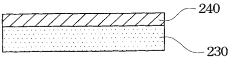
图2A-图2H绘示根据本发明的一实施例的一种软性电子装置的制作方法。相同地,需要平坦基材210,例如:玻璃、石英、塑胶、陶瓷或金属基材,来制造软性电子装置。基材210通常具有平坦上(第一)表面212与相对的第二表面214。2A-2H illustrate a manufacturing method of a flexible electronic device according to an embodiment of the present invention. Similarly, a
此方法始于以抗剥离材料形成抗剥离层220在基材210的平坦上表面212上,此抗剥离材料包含金属氧化物,如图2A所示。在一实施例中,形成抗剥离层220的步骤包含溅镀抗剥离材料于基材210的平坦上表面212上。在另一实施例中,形成抗剥离层220的步骤包含气相涂布抗剥离材料在基材210的平坦上表面212上。在一实施例中,抗剥离材料包含氧化铟锡(Indium Tin Oxide;ITO)。可理解的是其他抗剥离材料与其他材料沉积工艺亦可用以实施本发明。The method begins with forming an
下一步骤图案化抗剥离层220,以在基材210中定义出第一区域211与第二区域213,第二区域213围绕第一区域211。在一实施例中,图案化抗剥离层220的步骤包含定义抗剥离层220上方的具有对应于第一区域211与第二区域213的图案的光阻226;以蚀刻剂或等离子228蚀刻第一区域211上的抗剥离层;及移除第二区域213上的光阻226,如图2B与图2C所示。此工艺以光学光刻或其他类似方式进行。The next step is to pattern the
在一实施例中,图案化第一区域211中的抗剥离层220,以完全地暴露基材210的上表面212,如图2C所示,因而抗剥离层220仅位于第二区域213上。In one embodiment, the
在另一实施例中,图案化第一区域211中的抗剥离层220,以局部地暴露出基材210的上表面212,如图2D所示。如此,抗剥离层220不仅在第二区域213上,且具有图案222的部分也位于第一区域211上,此图案222改善介于塑胶层230(描述如下)与基材210间的结合,以便调整介于其间的附着力。如图2D所示,图案222为网纹图案。亦可使用其他图案,例如狭缝图案与岛型图案。在一实施例中,第一区域211的未暴露部分(即图案化后的部分)约为第一区域211的0.1%至30.0%,且第二区域213的面积大于第一区域211的未暴露部分的面积。In another embodiment, the
在又一实施例中,如图2E所示,图案化抗剥离层220,以局部地暴露出基材210的上表面212,借以在第一区域211与第二区域213上分别形成抗剥离层220的图案222与图案224。此些图案222与223改善介于塑胶层230(描述如下)与基材210间的结合,以便调整介于其间的附着力。如图2E所示,图案222与224均为网纹图案。在其他实施例中,亦可使用其他图案,例如狭缝图案与岛型图案。在一实施例中,第二区域213的未暴露部分的密度(即第二区域213的单位面积中,图案224的面积)大于第一区域211的未暴露部分的密度(即第一区域211的单位面积中,图案222的面积)。在一实施例中,第二区域213中的抗剥离层220的总面积可大于第一区域211中的抗剥离层220的总面积。在另一实施例中,第二区域213中的抗剥离层220的总面积亦可等于或小于第一区域211中的抗剥离层220的总面积。In yet another embodiment, as shown in FIG. 2E , the
再者,以聚亚酰胺形成塑胶层230在第一区域211与第二区域213上方的抗剥离层220上,如图2F所示。因此,塑胶层230与第一区域211中的基材210间的附着力较塑胶层230与第二区域213中的抗剥离层220间的附着力弱。在一实施例中,形成塑胶层230的步骤包含以聚酰胺酸涂布第一区域211及第二区域213上的抗剥离层220,以于第一区域211与抗剥离层220上形成聚酰胺酸层;及固化此涂布的聚酰胺酸层,以形成塑胶层230。Furthermore, the
在塑胶层230上,形成电子装置层240于第一区域211上,其中电子装置层240于第一区域211上界定出边界242,如图2G所示。边界242投影地位于第一区域211中。电子装置层240可为一或多个TFTs或任何其他电子零件。On the
然后,通过沿着一轮廓来切穿塑胶层230,而将电子装置层240和塑胶层230与基材210分离,此轮廓相等于或大于电子装置层240的边界242,但不超出第一区域211,如图2H所示。由于塑胶层230与第一区域211中的基材210间的附着力比塑胶层230与第二区域213中的抗剥离层220间的附着力弱,因此将很容易的从基材210分离电子装置层240与第一区域211中的塑胶层230。The
现在请参考图3A-图3H,其绘示根据本发明的一实施例的一种软性电子装置的制作方法。此方法包含以下步骤:首先,提供基材310,基材310具有平坦的上表面312与相对的第二表面314。相同地,基材310可为玻璃、石英、塑胶、陶瓷、金属或类似材料的基材。Please refer now to FIG. 3A-FIG. 3H , which illustrate a manufacturing method of a flexible electronic device according to an embodiment of the present invention. The method includes the following steps: firstly, a
下一步骤涂布第一聚酰胺酸于基材310的平坦上表面312上,以形成第一聚亚酰胺层320,借此定义出基材310中的第一区域311与第二区域313(详述于后),第一聚亚酰胺层320形成于第一区域311上,且第二区域313围绕第一区域311,如图3B与图3C所示。进行涂布步骤时可通过施加过量的聚酰胺酸溶液至平坦基材310的上表面312,如图3A所示,然后在高转速下旋转聚酰胺酸溶液与基材310,以散开聚酰胺酸溶液,而形成涂布于基材310上的第一聚酰胺酸层,在约70℃至250℃的温度下,对涂布后的聚酰胺酸层进行约5分钟至30分钟的烘烤,较佳地在约150℃下烘烤约10分钟,然后在约200℃至400℃的温度下,对烘烤后的聚酰胺酸层进行固化约30分钟至60分钟,较佳地在约300℃下进行约60分钟,以形成第一聚亚酰胺层320。此外,可通过切割工艺,亦即沿着轮廓311A切穿第一聚亚酰胺层320,来定义出第一区域311与第二区域313,借以定义出位于轮廓311A内的第一区域311、与围绕第一区域311的第二区域313;以及剥除第二区域313上的第一聚亚酰胺层320的部分,如图3C与图3D所示。如此一来,第一聚亚酰胺层320仅位于第一区域311上,而暴露出第二区域313中的基材310。The next step is to coat the first polyamic acid on the flat upper surface 312 of the
然后,将含有有机硅烷的第二聚酰胺酸涂布于基材310的第一区域311中的第一聚亚酰胺层320上、与基材310的第二区域313上,以在第一聚亚酰胺层320与第二区域313上形成第二聚亚酰胺层330,如图3E与图3F所示。借此,第一聚亚酰胺层320与第一区域311的基材310间的附着力较第二聚亚酰胺层330与第二区域313中的基材310间的附着力弱。相同地,进行涂布步骤时通过施加一些含有机硅烷的第二聚酰胺酸至第一聚亚酰胺层320的上表面322,如图3E所示,然后在高转速下旋转第二聚酰胺酸与基材310,以散开此混合物,而形成含有机硅烷的第二聚酰胺酸层且涂布于第一聚亚酰胺层320上,在约70℃至250℃间的温度下,对上述的结构烘烤约5分钟至30分钟,较佳地在约150℃下烘烤10分钟,然后在约200℃至400℃间的温度下,对第二聚酰胺酸层进行约30分钟至60分钟的固化,较佳地在约300℃进行约60分钟的固化,以形成第二聚亚酰胺层330。第一聚酰胺酸与第二聚酰胺酸可相同或彼此实质上不同。Then, the second polyamic acid containing organosilane is coated on the
在第二聚亚酰胺层330上,形成电子装置层340在第一区域311上,其中电子装置层340在第一区域311上界定出边界342,如图3G所示。边界342投影地位于第一区域311内。电子装置层340可为一或多个TFTs或任何其他电子零件。On the
接着,通过沿着一轮廓来切穿第一聚亚酰胺层320与第二聚亚酰胺层330,而将电子装置层340、第一聚亚酰胺层320和第二聚亚酰胺层330与基材310分离,此轮廓相等于或大于电子装置层340的边界342,但不超出第一区域311,如图3H所示。由于第一聚亚酰胺层320与第一区域311的基材310间的附着力较第二聚亚酰胺层330与第二区域313中的基材310间的附着力弱,因此将很容易从基材310分离电子装置层340、第一聚亚酰胺层320与第一区域311中的第二聚亚酰胺层330。Next, by cutting through the
在本发明的一态样中,一种软性电子装置的制作方法,包含:提供基材,此基材具有第一表面与相对的第二表面;形成第一层于基材的第一表面上,以在基材中定义出第一区域与第二区域,第二区域围绕第一区域,如此基材在第一区域中的第一表面至少部分暴露出来,且第一层至少部分位于第二区域内;形成第二层在第一区域与第二区域上方的第一层上,如此第二层与第一区域中的基材间的附着力较第二层与第二区域中的第一层间的附着力弱;形成电子装置层于第一区域上方的第二层上,其中电子装置层于第一区域上定义出边界,且此边界投影地位于第一区域中;以及通过沿着一轮廓切穿第二层的方式,将电子装置层和第二层与基材分离,此轮廓相等于或大于电子装置层的边界,但不超出第一区域。In one aspect of the present invention, a method for manufacturing a flexible electronic device includes: providing a substrate, the substrate having a first surface and an opposite second surface; forming a first layer on the first surface of the substrate above, to define a first region and a second region in the substrate, the second region surrounds the first region, such that the first surface of the substrate in the first region is at least partially exposed, and the first layer is at least partially located in the second region. In the second area; forming a second layer on the first layer above the first area and the second area, such that the adhesion between the second layer and the substrate in the first area is better than that between the second layer and the first layer in the second area The adhesion between the layers is weak; the electronic device layer is formed on the second layer above the first area, wherein the electronic device layer defines a boundary on the first area, and the boundary is projectedly located in the first area; and by The electronic device layer and the second layer are separated from the substrate by cutting through the second layer with a contour equal to or greater than the boundary of the electronic device layer but not beyond the first region.
在一实施例中,形成第一层的步骤包含形成由助粘材料组成的助粘层于基材的第一表面上的步骤,其中助粘材料包含有机硅烷。In one embodiment, the step of forming the first layer includes the step of forming an adhesion-promoting layer composed of an adhesion-promoting material on the first surface of the substrate, wherein the adhesion-promoting material comprises organosilane.
在一实施例中,形成助粘层的步骤包含步骤:涂布助粘材料在基材的第一表面,以及于第一温度下烘烤涂布有助粘材料的基材第一段时间,以形成助粘层,其中第一温度的范围介于约50℃至250℃,且第一段时间的范围介于约5分钟至10分钟。在另一实施例中,形成第一层的步骤包含气相涂布助粘材料在基材的第一表面的步骤,以形成助粘层。In one embodiment, the step of forming the adhesion-promoting layer includes the steps of: coating the adhesion-promoting material on the first surface of the substrate, and baking the substrate coated with the adhesion-promoting material at a first temperature for a first period of time, To form an adhesion-promoting layer, wherein the first temperature ranges from about 50° C. to 250° C., and the first period of time ranges from about 5 minutes to 10 minutes. In another embodiment, the step of forming the first layer comprises a step of vapor-phase coating an adhesion-promoting material on the first surface of the substrate to form an adhesion-promoting layer.
在一实施例中,形成第一层的步骤更包含步骤:形成具有图案的掩膜于助粘层上的步骤,此图案对应于第一区域与第二区域;在空气或氧气的环境中,以UV光处理掩膜,如此UV光照射第一区域上的助黏层,而第二区域上的助黏层则被遮蔽而不受UV光照射;以及移除第一区域上的助黏层的部分。在一实施例中,处理步骤在第二温度下且在烘箱中进行第二段时间,其中第二温度的范围介于约25℃至300℃,且第二段时间的范围介于约1分钟至10分钟。In one embodiment, the step of forming the first layer further includes the step of: forming a mask with a pattern on the adhesion-promoting layer, the pattern corresponding to the first region and the second region; in an air or oxygen environment, treating the mask with UV light such that the UV light illuminates the adhesion promoting layer on the first area and the adhesion promoting layer on the second area is shielded from the UV light; and removing the adhesion promoting layer on the first area part. In one embodiment, the treating step is performed at a second temperature in an oven for a second period of time, wherein the second temperature ranges from about 25° C. to 300° C. and the second period of time ranges from about 1 minute. to 10 minutes.
在另一实施例中,形成第一层的步骤包含形成由抗剥离材料组成的抗剥离层于基材的第一表面上的步骤,抗剥离材料包含金属氧化物,其中抗剥离材料包含氧化铟锡。在一实施例中,形成抗剥离层的步骤包含溅镀或气相涂布抗剥离材料于基材的第一表面上的步骤。In another embodiment, the step of forming the first layer comprises the step of forming an anti-stripping layer composed of an anti-stripping material on the first surface of the substrate, the anti-stripping material comprising metal oxide, wherein the anti-stripping material comprises indium oxide tin. In one embodiment, the step of forming the anti-stripping layer includes the step of sputtering or vapor-phase coating an anti-stripping material on the first surface of the substrate.
在一实施例中,形成第一层的步骤更包含步骤:定义抗剥离层上的具有图案的光阻,此图案对应于第一区域与第二区域;以蚀刻剂或电浆蚀刻第一区域上的抗剥离层,借以至少部分地暴露出第一区域中的基材;以及移除光阻。在一实施例中,图案化第一区域,以使第一区域的未暴露部分约为第一区域的0.1%至30.0%,且第二区域的面积大于第一区域的未暴露部分的面积,其中第一区域的未暴露部分经图案化以具有狭缝图案、岛型图案或网纹图案。In one embodiment, the step of forming the first layer further includes the steps of: defining a photoresist with a pattern on the anti-stripping layer, the pattern corresponding to the first region and the second region; etching the first region with etchant or plasma an anti-peeling layer on the substrate, thereby at least partially exposing the substrate in the first region; and removing the photoresist. In one embodiment, the first region is patterned such that the unexposed portion of the first region is about 0.1% to 30.0% of the first region, and the area of the second region is greater than the area of the unexposed portion of the first region, Wherein the unexposed portion of the first region is patterned to have a slit pattern, an island pattern or a textured pattern.
在一实施例中,形成第二层的步骤包含步骤:以聚酰胺酸涂布第一区域与第二区域上方的第一层上,以于第一区域与第一层上形成涂布的聚酰胺酸层;以及固化涂布的聚酰胺酸层,以形成由聚亚酰胺所组成的第二层。In one embodiment, the step of forming the second layer includes the step of: coating the first layer above the first region and the second region with polyamic acid to form a coated polyamic acid on the first region and the first layer. an amic acid layer; and curing the coated polyamic acid layer to form a second layer composed of polyimide.
本发明的示范实施例的上述描述仅作为举例说明与描述之用,并非无所不包,也非用以将本发明限制在所公开的刻板型式。根据上述教示,可有许多修饰与变化。The foregoing description of exemplary embodiments of this invention has been presented for purposes of illustration and description, but is not intended to be all-inclusive or to limit the invention to the precise forms disclosed. Many modifications and variations are possible in light of the above teaching.
当然,本发明还可有其它多种实施例,在不背离本发明精神及其实质的情况下,熟悉本领域的技术人员当可根据本发明作出各种相应的改变和变形,但这些相应的改变和变形都应属于本发明所附的权利要求的保护范围。Certainly, the present invention also can have other multiple embodiments, without departing from the spirit and essence of the present invention, those skilled in the art can make various corresponding changes and deformations according to the present invention, but these corresponding Changes and deformations should belong to the scope of protection of the appended claims of the present invention.
Claims (19)
Applications Claiming Priority (2)
| Application Number | Priority Date | Filing Date | Title |
|---|---|---|---|
| US13/292,599 | 2011-11-09 | ||
| US13/292,599 US20130115426A1 (en) | 2011-11-09 | 2011-11-09 | Method of manufacturing flexible electronic device |
Publications (2)
| Publication Number | Publication Date |
|---|---|
| CN102629593A CN102629593A (en) | 2012-08-08 |
| CN102629593B true CN102629593B (en) | 2014-04-02 |
Family
ID=45566853
Family Applications (1)
| Application Number | Title | Priority Date | Filing Date |
|---|---|---|---|
| CN201210092783.1A Active CN102629593B (en) | 2011-11-09 | 2012-03-29 | Flexible electronic device and manufacturing method thereof |
Country Status (4)
| Country | Link |
|---|---|
| US (1) | US20130115426A1 (en) |
| EP (1) | EP2592653B1 (en) |
| CN (1) | CN102629593B (en) |
| TW (1) | TWI444293B (en) |
Families Citing this family (13)
| Publication number | Priority date | Publication date | Assignee | Title |
|---|---|---|---|---|
| US9991311B2 (en) | 2008-12-02 | 2018-06-05 | Arizona Board Of Regents On Behalf Of Arizona State University | Dual active layer semiconductor device and method of manufacturing the same |
| EP2624326A4 (en) * | 2010-09-29 | 2017-05-10 | Posco | Method for manufacturing a flexible electronic device using a roll-shaped motherboard, flexible electronic device, and flexible substrate |
| TWI445626B (en) * | 2011-03-18 | 2014-07-21 | 長興化學工業股份有限公司 | Method of manufacturing a flexible component |
| JP6417330B2 (en) * | 2012-11-30 | 2018-11-07 | エルジー ディスプレイ カンパニー リミテッド | Organic light-emitting device including flexible substrate and method for manufacturing the same |
| TWI555637B (en) * | 2013-10-04 | 2016-11-01 | 財團法人工業技術研究院 | Release layer, substrate structure, and method for manufacturing flexible electronic device |
| CN104512075B (en) | 2013-10-04 | 2017-06-23 | 财团法人工业技术研究院 | Release layer, substrate structure and flexible electronic element process |
| WO2017034644A2 (en) * | 2015-06-09 | 2017-03-02 | ARIZONA BOARD OF REGENTS a body corporate for THE STATE OF ARIZONA for and on behalf of ARIZONA STATE UNIVERSITY | Method of providing an electronic device and electronic device thereof |
| US10381224B2 (en) * | 2014-01-23 | 2019-08-13 | Arizona Board Of Regents On Behalf Of Arizona State University | Method of providing an electronic device and electronic device thereof |
| JP2017518638A (en) * | 2014-05-13 | 2017-07-06 | アリゾナ・ボード・オブ・リージェンツ・フォー・アンド・オン・ビハーフ・オブ・アリゾナ・ステイト・ユニバーシティArizona Board Of Regents For And On Behalf Of Arizona State University | Method for providing an electronic device and the electronic device |
| US9741742B2 (en) | 2014-12-22 | 2017-08-22 | Arizona Board Of Regents, A Body Corporate Of The State Of Arizona, Acting For And On Behalf Of Arizona State University | Deformable electronic device and methods of providing and using deformable electronic device |
| US10446582B2 (en) | 2014-12-22 | 2019-10-15 | Arizona Board Of Regents On Behalf Of Arizona State University | Method of providing an imaging system and imaging system thereof |
| US10418237B2 (en) * | 2016-11-23 | 2019-09-17 | United States Of America As Represented By The Secretary Of The Air Force | Amorphous boron nitride dielectric |
| CN107507916B (en) * | 2017-08-11 | 2020-04-03 | 京东方科技集团股份有限公司 | A PI substrate, preparation method thereof, and display device |
Citations (4)
| Publication number | Priority date | Publication date | Assignee | Title |
|---|---|---|---|---|
| US5037701A (en) * | 1988-01-05 | 1991-08-06 | Corning Incorporated | Processes for producing colored glass or glass-ceramic articles bearing a non-stick coating, compositions for carrying out said processes, and resultant colored articles |
| CN101903974A (en) * | 2008-02-28 | 2010-12-01 | 夏普株式会社 | Method for manufacturing thin film laminated device, method for manufacturing display device, and thin film laminated device |
| CN102043300A (en) * | 2009-10-21 | 2011-05-04 | 乐金显示有限公司 | Methode of fabricating display device using flexible plastic substrate |
| CN102089858A (en) * | 2008-02-20 | 2011-06-08 | 夏普株式会社 | Manufacturing method of flexible semiconductor substrate |
Family Cites Families (6)
| Publication number | Priority date | Publication date | Assignee | Title |
|---|---|---|---|---|
| US7449372B2 (en) * | 2004-12-17 | 2008-11-11 | Semiconductor Energy Laboratory Co., Ltd. | Manufacturing method of substrate having conductive layer and manufacturing method of semiconductor device |
| TWI276191B (en) * | 2005-08-30 | 2007-03-11 | Ind Tech Res Inst | Alignment precision enhancement of electronic component process on flexible substrate device and method thereof the same |
| TWI265606B (en) * | 2005-09-19 | 2006-11-01 | Ind Tech Res Inst | Method of fabricating flexible thin film transistor array substrate |
| US7968382B2 (en) * | 2007-02-02 | 2011-06-28 | Semiconductor Energy Laboratory Co., Ltd. | Method of manufacturing semiconductor device |
| TWI354854B (en) * | 2008-09-15 | 2011-12-21 | Ind Tech Res Inst | Substrate structures applied in flexible electrica |
| KR101009415B1 (en) * | 2008-11-18 | 2011-01-19 | 삼성모바일디스플레이주식회사 | A method of manufacturing an electronic device having a plastic substrate, an electronic device manufactured thereby, and a device used in the manufacturing method |
-
2011
- 2011-11-09 US US13/292,599 patent/US20130115426A1/en not_active Abandoned
- 2011-12-28 TW TW100149228A patent/TWI444293B/en active
-
2012
- 2012-01-26 EP EP12152760.0A patent/EP2592653B1/en active Active
- 2012-03-29 CN CN201210092783.1A patent/CN102629593B/en active Active
Patent Citations (4)
| Publication number | Priority date | Publication date | Assignee | Title |
|---|---|---|---|---|
| US5037701A (en) * | 1988-01-05 | 1991-08-06 | Corning Incorporated | Processes for producing colored glass or glass-ceramic articles bearing a non-stick coating, compositions for carrying out said processes, and resultant colored articles |
| CN102089858A (en) * | 2008-02-20 | 2011-06-08 | 夏普株式会社 | Manufacturing method of flexible semiconductor substrate |
| CN101903974A (en) * | 2008-02-28 | 2010-12-01 | 夏普株式会社 | Method for manufacturing thin film laminated device, method for manufacturing display device, and thin film laminated device |
| CN102043300A (en) * | 2009-10-21 | 2011-05-04 | 乐金显示有限公司 | Methode of fabricating display device using flexible plastic substrate |
Also Published As
| Publication number | Publication date |
|---|---|
| US20130115426A1 (en) | 2013-05-09 |
| TW201318858A (en) | 2013-05-16 |
| EP2592653A1 (en) | 2013-05-15 |
| CN102629593A (en) | 2012-08-08 |
| TWI444293B (en) | 2014-07-11 |
| EP2592653B1 (en) | 2016-11-30 |
Similar Documents
| Publication | Publication Date | Title |
|---|---|---|
| CN102629593B (en) | Flexible electronic device and manufacturing method thereof | |
| TWI445626B (en) | Method of manufacturing a flexible component | |
| KR101156941B1 (en) | Method for isolating flexible film from support substrate | |
| TWI673167B (en) | Laminated product and method for producing flexible device | |
| CN104875462B (en) | Manufacturing method of display device, resin, resin solution, and peeling device | |
| KR101113849B1 (en) | Method for isolating flexible substrate from support substrate | |
| CN107206771A (en) | Laminate including metal wire layer and manufacturing method thereof | |
| CN108470849B (en) | Flexible substrate and manufacturing method thereof | |
| CN102969393A (en) | Method for patterning indium tin oxide film (ITO) film on substrate | |
| TWI703477B (en) | Film touch sensor and method for manufacturing the same | |
| CN103236418B (en) | Method for manufacturing flexible substrate | |
| CN108962937A (en) | Flexible display device and preparation method thereof | |
| CN107195658A (en) | Flexible substrate and manufacturing method thereof | |
| CN101435992B (en) | Photoresist pattern forming method | |
| CN108866478A (en) | Photomask manufacturing method and mask plate | |
| CN107845606B (en) | A kind of preparation method of TFT substrate and TFT substrate | |
| CN105278237B (en) | Photomask and method for manufacturing photomask | |
| JP2004157307A (en) | Method for manufacturing functional element | |
| JP7500946B2 (en) | Method for manufacturing deposition mask | |
| CN110791220A (en) | Transparent polyimide composite film for flexible display and manufacturing method thereof | |
| CN107768417B (en) | A display substrate, its preparation method, and display device | |
| JP2016055242A (en) | Manufacturing device of substrate with resin layer, manufacturing method of laminate, and manufacturing method of electronic device | |
| JP6556483B2 (en) | Substrate with electrode and method for manufacturing the same | |
| TW202007532A (en) | Transparent polyimide composite film for flexible display device and manufacturing method thereof including a transparent polyimide film, and an adhesive layer |
Legal Events
| Date | Code | Title | Description |
|---|---|---|---|
| C06 | Publication | ||
| PB01 | Publication | ||
| C10 | Entry into substantive examination | ||
| SE01 | Entry into force of request for substantive examination | ||
| C14 | Grant of patent or utility model | ||
| GR01 | Patent grant |