CN102592666A - Nonvolatile memory cell comprising a diode and a resistance-switching material - Google Patents
Nonvolatile memory cell comprising a diode and a resistance-switching material Download PDFInfo
- Publication number
- CN102592666A CN102592666A CN2011104479774A CN201110447977A CN102592666A CN 102592666 A CN102592666 A CN 102592666A CN 2011104479774 A CN2011104479774 A CN 2011104479774A CN 201110447977 A CN201110447977 A CN 201110447977A CN 102592666 A CN102592666 A CN 102592666A
- Authority
- CN
- China
- Prior art keywords
- conductor
- diode
- resistivity
- switching device
- resistance
- Prior art date
- Legal status (The legal status is an assumption and is not a legal conclusion. Google has not performed a legal analysis and makes no representation as to the accuracy of the status listed.)
- Pending
Links
- 230000015654 memory Effects 0.000 title claims abstract description 345
- 239000000463 material Substances 0.000 title claims abstract description 197
- 239000004020 conductor Substances 0.000 claims abstract description 220
- 229910044991 metal oxide Inorganic materials 0.000 claims abstract description 86
- GNPVGFCGXDBREM-UHFFFAOYSA-N germanium atom Chemical compound [Ge] GNPVGFCGXDBREM-UHFFFAOYSA-N 0.000 claims abstract description 69
- 229910052732 germanium Inorganic materials 0.000 claims abstract description 68
- -1 O y Chemical class 0.000 claims abstract description 64
- 239000000758 substrate Substances 0.000 claims abstract description 50
- 229910052782 aluminium Inorganic materials 0.000 claims abstract description 45
- 150000004706 metal oxides Chemical class 0.000 claims abstract description 31
- 229910000927 Ge alloy Inorganic materials 0.000 claims abstract description 28
- XAGFODPZIPBFFR-UHFFFAOYSA-N aluminium Chemical compound [Al] XAGFODPZIPBFFR-UHFFFAOYSA-N 0.000 claims abstract description 23
- RYGMFSIKBFXOCR-UHFFFAOYSA-N Copper Chemical compound [Cu] RYGMFSIKBFXOCR-UHFFFAOYSA-N 0.000 claims abstract description 15
- 229910052802 copper Inorganic materials 0.000 claims abstract description 15
- 239000010949 copper Substances 0.000 claims abstract description 15
- 238000000034 method Methods 0.000 claims description 138
- 239000004065 semiconductor Substances 0.000 claims description 79
- 229910021420 polycrystalline silicon Inorganic materials 0.000 claims description 49
- 229920005591 polysilicon Polymers 0.000 claims description 46
- XUIMIQQOPSSXEZ-UHFFFAOYSA-N Silicon Chemical compound [Si] XUIMIQQOPSSXEZ-UHFFFAOYSA-N 0.000 claims description 39
- 239000010703 silicon Substances 0.000 claims description 39
- 239000010936 titanium Substances 0.000 claims description 33
- 229910052710 silicon Inorganic materials 0.000 claims description 32
- 229910052751 metal Inorganic materials 0.000 claims description 28
- 239000002184 metal Substances 0.000 claims description 28
- PXHVJJICTQNCMI-UHFFFAOYSA-N nickel Substances [Ni] PXHVJJICTQNCMI-UHFFFAOYSA-N 0.000 claims description 28
- 239000010955 niobium Substances 0.000 claims description 28
- 239000011777 magnesium Substances 0.000 claims description 27
- 230000015572 biosynthetic process Effects 0.000 claims description 26
- 229910052719 titanium Inorganic materials 0.000 claims description 25
- 239000011651 chromium Substances 0.000 claims description 24
- 238000005530 etching Methods 0.000 claims description 24
- 238000000059 patterning Methods 0.000 claims description 23
- 229910000510 noble metal Inorganic materials 0.000 claims description 20
- 229910052804 chromium Inorganic materials 0.000 claims description 19
- 229910052735 hafnium Inorganic materials 0.000 claims description 19
- 229910052749 magnesium Inorganic materials 0.000 claims description 19
- 229910052758 niobium Inorganic materials 0.000 claims description 19
- 229910052720 vanadium Inorganic materials 0.000 claims description 19
- 238000000151 deposition Methods 0.000 claims description 15
- 238000002425 crystallisation Methods 0.000 claims description 13
- 230000008025 crystallization Effects 0.000 claims description 13
- WFKWXMTUELFFGS-UHFFFAOYSA-N tungsten Chemical compound [W] WFKWXMTUELFFGS-UHFFFAOYSA-N 0.000 claims description 12
- 229910052721 tungsten Inorganic materials 0.000 claims description 12
- 239000010937 tungsten Substances 0.000 claims description 12
- 230000008021 deposition Effects 0.000 claims description 10
- RTAQQCXQSZGOHL-UHFFFAOYSA-N Titanium Chemical compound [Ti] RTAQQCXQSZGOHL-UHFFFAOYSA-N 0.000 claims description 8
- 229910045601 alloy Inorganic materials 0.000 claims description 7
- 239000000956 alloy Substances 0.000 claims description 7
- 238000011049 filling Methods 0.000 claims description 6
- 229910021421 monocrystalline silicon Inorganic materials 0.000 claims description 6
- ZOXJGFHDIHLPTG-UHFFFAOYSA-N Boron Chemical compound [B] ZOXJGFHDIHLPTG-UHFFFAOYSA-N 0.000 claims description 4
- 229910052796 boron Inorganic materials 0.000 claims description 4
- 229910017052 cobalt Inorganic materials 0.000 claims description 3
- 239000010941 cobalt Substances 0.000 claims description 3
- GUTLYIVDDKVIGB-UHFFFAOYSA-N cobalt atom Chemical compound [Co] GUTLYIVDDKVIGB-UHFFFAOYSA-N 0.000 claims description 3
- 229910000838 Al alloy Inorganic materials 0.000 claims description 2
- VYZAMTAEIAYCRO-UHFFFAOYSA-N Chromium Chemical compound [Cr] VYZAMTAEIAYCRO-UHFFFAOYSA-N 0.000 claims description 2
- GYHNNYVSQQEPJS-UHFFFAOYSA-N Gallium Chemical compound [Ga] GYHNNYVSQQEPJS-UHFFFAOYSA-N 0.000 claims description 2
- FYYHWMGAXLPEAU-UHFFFAOYSA-N Magnesium Chemical compound [Mg] FYYHWMGAXLPEAU-UHFFFAOYSA-N 0.000 claims description 2
- 229910010413 TiO 2 Inorganic materials 0.000 claims description 2
- QCWXUUIWCKQGHC-UHFFFAOYSA-N Zirconium Chemical compound [Zr] QCWXUUIWCKQGHC-UHFFFAOYSA-N 0.000 claims description 2
- 229910052733 gallium Inorganic materials 0.000 claims description 2
- 229910052737 gold Inorganic materials 0.000 claims description 2
- VBJZVLUMGGDVMO-UHFFFAOYSA-N hafnium atom Chemical compound [Hf] VBJZVLUMGGDVMO-UHFFFAOYSA-N 0.000 claims description 2
- 229910052738 indium Inorganic materials 0.000 claims description 2
- APFVFJFRJDLVQX-UHFFFAOYSA-N indium atom Chemical compound [In] APFVFJFRJDLVQX-UHFFFAOYSA-N 0.000 claims description 2
- 229910052741 iridium Inorganic materials 0.000 claims description 2
- 229910052746 lanthanum Inorganic materials 0.000 claims description 2
- FZLIPJUXYLNCLC-UHFFFAOYSA-N lanthanum atom Chemical compound [La] FZLIPJUXYLNCLC-UHFFFAOYSA-N 0.000 claims description 2
- WPBNNNQJVZRUHP-UHFFFAOYSA-L manganese(2+);methyl n-[[2-(methoxycarbonylcarbamothioylamino)phenyl]carbamothioyl]carbamate;n-[2-(sulfidocarbothioylamino)ethyl]carbamodithioate Chemical compound [Mn+2].[S-]C(=S)NCCNC([S-])=S.COC(=O)NC(=S)NC1=CC=CC=C1NC(=S)NC(=O)OC WPBNNNQJVZRUHP-UHFFFAOYSA-L 0.000 claims description 2
- 229910052759 nickel Inorganic materials 0.000 claims description 2
- GUCVJGMIXFAOAE-UHFFFAOYSA-N niobium atom Chemical compound [Nb] GUCVJGMIXFAOAE-UHFFFAOYSA-N 0.000 claims description 2
- 229910052763 palladium Inorganic materials 0.000 claims description 2
- 229910052697 platinum Inorganic materials 0.000 claims description 2
- 229910052715 tantalum Inorganic materials 0.000 claims description 2
- GUVRBAGPIYLISA-UHFFFAOYSA-N tantalum atom Chemical compound [Ta] GUVRBAGPIYLISA-UHFFFAOYSA-N 0.000 claims description 2
- GPPXJZIENCGNKB-UHFFFAOYSA-N vanadium Chemical compound [V]#[V] GPPXJZIENCGNKB-UHFFFAOYSA-N 0.000 claims description 2
- 229910052727 yttrium Inorganic materials 0.000 claims description 2
- VWQVUPCCIRVNHF-UHFFFAOYSA-N yttrium atom Chemical compound [Y] VWQVUPCCIRVNHF-UHFFFAOYSA-N 0.000 claims description 2
- 229910052726 zirconium Inorganic materials 0.000 claims description 2
- 229910052725 zinc Inorganic materials 0.000 claims 17
- 239000004411 aluminium Substances 0.000 claims 9
- 229910000676 Si alloy Inorganic materials 0.000 claims 8
- 238000003475 lamination Methods 0.000 claims 4
- 230000002441 reversible effect Effects 0.000 abstract description 42
- 150000004767 nitrides Chemical class 0.000 abstract description 23
- 150000001875 compounds Chemical class 0.000 abstract description 13
- 239000010410 layer Substances 0.000 description 191
- 229910000480 nickel oxide Inorganic materials 0.000 description 36
- GNRSAWUEBMWBQH-UHFFFAOYSA-N oxonickel Chemical compound [Ni]=O GNRSAWUEBMWBQH-UHFFFAOYSA-N 0.000 description 36
- 230000004888 barrier function Effects 0.000 description 28
- 238000003491 array Methods 0.000 description 23
- 238000004519 manufacturing process Methods 0.000 description 17
- NRTOMJZYCJJWKI-UHFFFAOYSA-N Titanium nitride Chemical compound [Ti]#N NRTOMJZYCJJWKI-UHFFFAOYSA-N 0.000 description 16
- 230000008569 process Effects 0.000 description 15
- 230000007704 transition Effects 0.000 description 14
- 229910021332 silicide Inorganic materials 0.000 description 13
- VYPSYNLAJGMNEJ-UHFFFAOYSA-N Silicium dioxide Chemical compound O=[Si]=O VYPSYNLAJGMNEJ-UHFFFAOYSA-N 0.000 description 11
- FVBUAEGBCNSCDD-UHFFFAOYSA-N silicide(4-) Chemical compound [Si-4] FVBUAEGBCNSCDD-UHFFFAOYSA-N 0.000 description 11
- 239000003989 dielectric material Substances 0.000 description 10
- 230000007547 defect Effects 0.000 description 8
- 238000005468 ion implantation Methods 0.000 description 7
- 229910000577 Silicon-germanium Inorganic materials 0.000 description 6
- LEVVHYCKPQWKOP-UHFFFAOYSA-N [Si].[Ge] Chemical compound [Si].[Ge] LEVVHYCKPQWKOP-UHFFFAOYSA-N 0.000 description 6
- 239000002019 doping agent Substances 0.000 description 5
- 238000011065 in-situ storage Methods 0.000 description 5
- 150000002739 metals Chemical class 0.000 description 5
- 238000000206 photolithography Methods 0.000 description 5
- 229910052814 silicon oxide Inorganic materials 0.000 description 5
- 239000011701 zinc Substances 0.000 description 5
- 238000007796 conventional method Methods 0.000 description 4
- 230000001965 increasing effect Effects 0.000 description 4
- 229920002120 photoresistant polymer Polymers 0.000 description 4
- 235000012431 wafers Nutrition 0.000 description 4
- 206010010144 Completed suicide Diseases 0.000 description 3
- 229910052581 Si3N4 Inorganic materials 0.000 description 3
- 239000012790 adhesive layer Substances 0.000 description 3
- 230000008901 benefit Effects 0.000 description 3
- 230000015556 catabolic process Effects 0.000 description 3
- 238000005229 chemical vapour deposition Methods 0.000 description 3
- 208000037265 diseases, disorders, signs and symptoms Diseases 0.000 description 3
- 208000035475 disorder Diseases 0.000 description 3
- 238000002955 isolation Methods 0.000 description 3
- 230000000873 masking effect Effects 0.000 description 3
- 235000012239 silicon dioxide Nutrition 0.000 description 3
- 239000000377 silicon dioxide Substances 0.000 description 3
- HQVNEWCFYHHQES-UHFFFAOYSA-N silicon nitride Chemical compound N12[Si]34N5[Si]62N3[Si]51N64 HQVNEWCFYHHQES-UHFFFAOYSA-N 0.000 description 3
- IJGRMHOSHXDMSA-UHFFFAOYSA-N Atomic nitrogen Chemical compound N#N IJGRMHOSHXDMSA-UHFFFAOYSA-N 0.000 description 2
- AXQKVSDUCKWEKE-UHFFFAOYSA-N [C].[Ge].[Si] Chemical compound [C].[Ge].[Si] AXQKVSDUCKWEKE-UHFFFAOYSA-N 0.000 description 2
- 239000000654 additive Substances 0.000 description 2
- 239000006117 anti-reflective coating Substances 0.000 description 2
- 230000002950 deficient Effects 0.000 description 2
- 230000000694 effects Effects 0.000 description 2
- 239000012777 electrically insulating material Substances 0.000 description 2
- 239000000945 filler Substances 0.000 description 2
- 239000011810 insulating material Substances 0.000 description 2
- 229920000642 polymer Polymers 0.000 description 2
- 239000010970 precious metal Substances 0.000 description 2
- 229910021341 titanium silicide Inorganic materials 0.000 description 2
- 230000009466 transformation Effects 0.000 description 2
- PFNQVRZLDWYSCW-UHFFFAOYSA-N (fluoren-9-ylideneamino) n-naphthalen-1-ylcarbamate Chemical compound C12=CC=CC=C2C2=CC=CC=C2C1=NOC(=O)NC1=CC=CC2=CC=CC=C12 PFNQVRZLDWYSCW-UHFFFAOYSA-N 0.000 description 1
- 229910018072 Al 2 O 3 Inorganic materials 0.000 description 1
- JBRZTFJDHDCESZ-UHFFFAOYSA-N AsGa Chemical compound [As]#[Ga] JBRZTFJDHDCESZ-UHFFFAOYSA-N 0.000 description 1
- OKTJSMMVPCPJKN-UHFFFAOYSA-N Carbon Chemical compound [C] OKTJSMMVPCPJKN-UHFFFAOYSA-N 0.000 description 1
- 229910001218 Gallium arsenide Inorganic materials 0.000 description 1
- GPXJNWSHGFTCBW-UHFFFAOYSA-N Indium phosphide Chemical compound [In]#P GPXJNWSHGFTCBW-UHFFFAOYSA-N 0.000 description 1
- 229910008479 TiSi2 Inorganic materials 0.000 description 1
- 230000000996 additive effect Effects 0.000 description 1
- 238000000137 annealing Methods 0.000 description 1
- 238000013459 approach Methods 0.000 description 1
- 238000004380 ashing Methods 0.000 description 1
- QVGXLLKOCUKJST-UHFFFAOYSA-N atomic oxygen Chemical compound [O] QVGXLLKOCUKJST-UHFFFAOYSA-N 0.000 description 1
- 230000009286 beneficial effect Effects 0.000 description 1
- DFJQEGUNXWZVAH-UHFFFAOYSA-N bis($l^{2}-silanylidene)titanium Chemical compound [Si]=[Ti]=[Si] DFJQEGUNXWZVAH-UHFFFAOYSA-N 0.000 description 1
- 229910052799 carbon Inorganic materials 0.000 description 1
- 150000004770 chalcogenides Chemical class 0.000 description 1
- 238000006243 chemical reaction Methods 0.000 description 1
- 239000011248 coating agent Substances 0.000 description 1
- 238000000576 coating method Methods 0.000 description 1
- 230000003750 conditioning effect Effects 0.000 description 1
- 238000010276 construction Methods 0.000 description 1
- 239000000356 contaminant Substances 0.000 description 1
- 238000011109 contamination Methods 0.000 description 1
- 230000007423 decrease Effects 0.000 description 1
- 238000009792 diffusion process Methods 0.000 description 1
- 230000002708 enhancing effect Effects 0.000 description 1
- 230000001747 exhibiting effect Effects 0.000 description 1
- 238000002474 experimental method Methods 0.000 description 1
- 230000002349 favourable effect Effects 0.000 description 1
- SCCCLDWUZODEKG-UHFFFAOYSA-N germanide Chemical compound [GeH3-] SCCCLDWUZODEKG-UHFFFAOYSA-N 0.000 description 1
- BHEPBYXIRTUNPN-UHFFFAOYSA-N hydridophosphorus(.) (triplet) Chemical compound [PH] BHEPBYXIRTUNPN-UHFFFAOYSA-N 0.000 description 1
- 238000002513 implantation Methods 0.000 description 1
- 239000012212 insulator Substances 0.000 description 1
- 239000007788 liquid Substances 0.000 description 1
- 230000007246 mechanism Effects 0.000 description 1
- 230000008018 melting Effects 0.000 description 1
- 238000002844 melting Methods 0.000 description 1
- 239000000203 mixture Substances 0.000 description 1
- 230000007935 neutral effect Effects 0.000 description 1
- 229910052757 nitrogen Inorganic materials 0.000 description 1
- 229910052760 oxygen Inorganic materials 0.000 description 1
- 239000001301 oxygen Substances 0.000 description 1
- 238000005268 plasma chemical vapour deposition Methods 0.000 description 1
- 238000001020 plasma etching Methods 0.000 description 1
- 238000005498 polishing Methods 0.000 description 1
- 238000012545 processing Methods 0.000 description 1
- 238000002310 reflectometry Methods 0.000 description 1
- 239000002002 slurry Substances 0.000 description 1
- 239000002904 solvent Substances 0.000 description 1
- 238000004544 sputter deposition Methods 0.000 description 1
- 239000000126 substance Substances 0.000 description 1
- 229910052723 transition metal Inorganic materials 0.000 description 1
- 150000003624 transition metals Chemical class 0.000 description 1
Images


Classifications
-
- G—PHYSICS
- G11—INFORMATION STORAGE
- G11C—STATIC STORES
- G11C11/00—Digital stores characterised by the use of particular electric or magnetic storage elements; Storage elements therefor
- G11C11/56—Digital stores characterised by the use of particular electric or magnetic storage elements; Storage elements therefor using storage elements with more than two stable states represented by steps, e.g. of voltage, current, phase, frequency
- G11C11/5685—Digital stores characterised by the use of particular electric or magnetic storage elements; Storage elements therefor using storage elements with more than two stable states represented by steps, e.g. of voltage, current, phase, frequency using storage elements comprising metal oxide memory material, e.g. perovskites
-
- H—ELECTRICITY
- H10—SEMICONDUCTOR DEVICES; ELECTRIC SOLID-STATE DEVICES NOT OTHERWISE PROVIDED FOR
- H10B—ELECTRONIC MEMORY DEVICES
- H10B63/00—Resistance change memory devices, e.g. resistive RAM [ReRAM] devices
- H10B63/80—Arrangements comprising multiple bistable or multi-stable switching components of the same type on a plane parallel to the substrate, e.g. cross-point arrays
-
- G—PHYSICS
- G11—INFORMATION STORAGE
- G11C—STATIC STORES
- G11C13/00—Digital stores characterised by the use of storage elements not covered by groups G11C11/00, G11C23/00, or G11C25/00
- G11C13/0002—Digital stores characterised by the use of storage elements not covered by groups G11C11/00, G11C23/00, or G11C25/00 using resistive RAM [RRAM] elements
- G11C13/0007—Digital stores characterised by the use of storage elements not covered by groups G11C11/00, G11C23/00, or G11C25/00 using resistive RAM [RRAM] elements comprising metal oxide memory material, e.g. perovskites
-
- G—PHYSICS
- G11—INFORMATION STORAGE
- G11C—STATIC STORES
- G11C13/00—Digital stores characterised by the use of storage elements not covered by groups G11C11/00, G11C23/00, or G11C25/00
- G11C13/0002—Digital stores characterised by the use of storage elements not covered by groups G11C11/00, G11C23/00, or G11C25/00 using resistive RAM [RRAM] elements
- G11C13/0021—Auxiliary circuits
- G11C13/0069—Writing or programming circuits or methods
-
- H—ELECTRICITY
- H10—SEMICONDUCTOR DEVICES; ELECTRIC SOLID-STATE DEVICES NOT OTHERWISE PROVIDED FOR
- H10B—ELECTRONIC MEMORY DEVICES
- H10B63/00—Resistance change memory devices, e.g. resistive RAM [ReRAM] devices
- H10B63/20—Resistance change memory devices, e.g. resistive RAM [ReRAM] devices comprising selection components having two electrodes, e.g. diodes
-
- H—ELECTRICITY
- H10—SEMICONDUCTOR DEVICES; ELECTRIC SOLID-STATE DEVICES NOT OTHERWISE PROVIDED FOR
- H10B—ELECTRONIC MEMORY DEVICES
- H10B63/00—Resistance change memory devices, e.g. resistive RAM [ReRAM] devices
- H10B63/80—Arrangements comprising multiple bistable or multi-stable switching components of the same type on a plane parallel to the substrate, e.g. cross-point arrays
- H10B63/84—Arrangements comprising multiple bistable or multi-stable switching components of the same type on a plane parallel to the substrate, e.g. cross-point arrays arranged in a direction perpendicular to the substrate, e.g. 3D cell arrays
- H10B63/845—Arrangements comprising multiple bistable or multi-stable switching components of the same type on a plane parallel to the substrate, e.g. cross-point arrays arranged in a direction perpendicular to the substrate, e.g. 3D cell arrays the switching components being connected to a common vertical conductor
-
- H—ELECTRICITY
- H10—SEMICONDUCTOR DEVICES; ELECTRIC SOLID-STATE DEVICES NOT OTHERWISE PROVIDED FOR
- H10D—INORGANIC ELECTRIC SEMICONDUCTOR DEVICES
- H10D64/00—Electrodes of devices having potential barriers
- H10D64/60—Electrodes characterised by their materials
- H10D64/66—Electrodes having a conductor capacitively coupled to a semiconductor by an insulator, e.g. MIS electrodes
- H10D64/68—Electrodes having a conductor capacitively coupled to a semiconductor by an insulator, e.g. MIS electrodes characterised by the insulator, e.g. by the gate insulator
- H10D64/691—Electrodes having a conductor capacitively coupled to a semiconductor by an insulator, e.g. MIS electrodes characterised by the insulator, e.g. by the gate insulator comprising metallic compounds, e.g. metal oxides or metal silicates
-
- H—ELECTRICITY
- H10—SEMICONDUCTOR DEVICES; ELECTRIC SOLID-STATE DEVICES NOT OTHERWISE PROVIDED FOR
- H10D—INORGANIC ELECTRIC SEMICONDUCTOR DEVICES
- H10D84/00—Integrated devices formed in or on semiconductor substrates that comprise only semiconducting layers, e.g. on Si wafers or on GaAs-on-Si wafers
- H10D84/201—Integrated devices formed in or on semiconductor substrates that comprise only semiconducting layers, e.g. on Si wafers or on GaAs-on-Si wafers characterised by the integration of only components covered by H10D1/00 or H10D8/00, e.g. RLC circuits
- H10D84/204—Integrated devices formed in or on semiconductor substrates that comprise only semiconducting layers, e.g. on Si wafers or on GaAs-on-Si wafers characterised by the integration of only components covered by H10D1/00 or H10D8/00, e.g. RLC circuits of combinations of diodes or capacitors or resistors
- H10D84/206—Integrated devices formed in or on semiconductor substrates that comprise only semiconducting layers, e.g. on Si wafers or on GaAs-on-Si wafers characterised by the integration of only components covered by H10D1/00 or H10D8/00, e.g. RLC circuits of combinations of diodes or capacitors or resistors of combinations of capacitors and resistors
-
- H—ELECTRICITY
- H10—SEMICONDUCTOR DEVICES; ELECTRIC SOLID-STATE DEVICES NOT OTHERWISE PROVIDED FOR
- H10N—ELECTRIC SOLID-STATE DEVICES NOT OTHERWISE PROVIDED FOR
- H10N70/00—Solid-state devices having no potential barriers, and specially adapted for rectifying, amplifying, oscillating or switching
- H10N70/20—Multistable switching devices, e.g. memristors
-
- H—ELECTRICITY
- H10—SEMICONDUCTOR DEVICES; ELECTRIC SOLID-STATE DEVICES NOT OTHERWISE PROVIDED FOR
- H10N—ELECTRIC SOLID-STATE DEVICES NOT OTHERWISE PROVIDED FOR
- H10N70/00—Solid-state devices having no potential barriers, and specially adapted for rectifying, amplifying, oscillating or switching
- H10N70/801—Constructional details of multistable switching devices
- H10N70/881—Switching materials
- H10N70/883—Oxides or nitrides
-
- G—PHYSICS
- G11—INFORMATION STORAGE
- G11C—STATIC STORES
- G11C13/00—Digital stores characterised by the use of storage elements not covered by groups G11C11/00, G11C23/00, or G11C25/00
- G11C13/0002—Digital stores characterised by the use of storage elements not covered by groups G11C11/00, G11C23/00, or G11C25/00 using resistive RAM [RRAM] elements
- G11C13/0021—Auxiliary circuits
- G11C13/0069—Writing or programming circuits or methods
- G11C2013/009—Write using potential difference applied between cell electrodes
-
- G—PHYSICS
- G11—INFORMATION STORAGE
- G11C—STATIC STORES
- G11C2213/00—Indexing scheme relating to G11C13/00 for features not covered by this group
- G11C2213/10—Resistive cells; Technology aspects
- G11C2213/15—Current-voltage curve
-
- G—PHYSICS
- G11—INFORMATION STORAGE
- G11C—STATIC STORES
- G11C2213/00—Indexing scheme relating to G11C13/00 for features not covered by this group
- G11C2213/30—Resistive cell, memory material aspects
- G11C2213/32—Material having simple binary metal oxide structure
-
- G—PHYSICS
- G11—INFORMATION STORAGE
- G11C—STATIC STORES
- G11C2213/00—Indexing scheme relating to G11C13/00 for features not covered by this group
- G11C2213/30—Resistive cell, memory material aspects
- G11C2213/34—Material includes an oxide or a nitride
-
- G—PHYSICS
- G11—INFORMATION STORAGE
- G11C—STATIC STORES
- G11C2213/00—Indexing scheme relating to G11C13/00 for features not covered by this group
- G11C2213/70—Resistive array aspects
- G11C2213/71—Three dimensional array
-
- G—PHYSICS
- G11—INFORMATION STORAGE
- G11C—STATIC STORES
- G11C2213/00—Indexing scheme relating to G11C13/00 for features not covered by this group
- G11C2213/70—Resistive array aspects
- G11C2213/72—Array wherein the access device being a diode
-
- H—ELECTRICITY
- H10—SEMICONDUCTOR DEVICES; ELECTRIC SOLID-STATE DEVICES NOT OTHERWISE PROVIDED FOR
- H10N—ELECTRIC SOLID-STATE DEVICES NOT OTHERWISE PROVIDED FOR
- H10N70/00—Solid-state devices having no potential barriers, and specially adapted for rectifying, amplifying, oscillating or switching
- H10N70/801—Constructional details of multistable switching devices
- H10N70/821—Device geometry
- H10N70/826—Device geometry adapted for essentially vertical current flow, e.g. sandwich or pillar type devices
-
- H—ELECTRICITY
- H10—SEMICONDUCTOR DEVICES; ELECTRIC SOLID-STATE DEVICES NOT OTHERWISE PROVIDED FOR
- H10N—ELECTRIC SOLID-STATE DEVICES NOT OTHERWISE PROVIDED FOR
- H10N70/00—Solid-state devices having no potential barriers, and specially adapted for rectifying, amplifying, oscillating or switching
- H10N70/801—Constructional details of multistable switching devices
- H10N70/881—Switching materials
- H10N70/883—Oxides or nitrides
- H10N70/8833—Binary metal oxides, e.g. TaOx
Landscapes
- Engineering & Computer Science (AREA)
- Chemical & Material Sciences (AREA)
- Materials Engineering (AREA)
- Computer Hardware Design (AREA)
- Semiconductor Memories (AREA)
Abstract
本发明涉及包括二极管和电阻切换材料的非易失性存储器单元。在一种形成于衬底上方的新颖的非易失性存储器单元中,二极管与可逆电阻切换材料配对,所述材料优选为例如NixOy、NbxOy、TixOy、HdxOy、AlxOy、MgxOy、CoxOy、CrxOy、VxOy、ZnxOy、ZrxOy、BxNy和AlxNy等金属氧化物或氮化物。在优选实施例中,所述二极管形成为设置在导体之间的垂直支柱。可堆叠多个存储器层级以形成单片三维存储器阵列。在一些实施例中,所述二极管包括锗或锗合金,其可在相对较低温度下沉积和结晶,从而允许在所述导体中使用铝或铜。本发明的存储器单元可用作可重写存储器单元或一次性可编程存储器单元,且可存储两种或两种以上数据状态。
The present invention relates to a non-volatile memory cell comprising a diode and a resistance-switching material. In a novel non-volatile memory cell formed above a substrate, a diode is paired with a reversible resistance-switching material, preferably Ni x O y , Nb x O y , Ti x O y , Hd x Metal oxides such as O y , Al x O y , Mg x O y , Co x O y , Cr x O y , V x O y , Zn x O y , Zr x O y , B x N y and Al x N y compounds or nitrides. In a preferred embodiment, the diodes are formed as vertical pillars arranged between conductors. Multiple memory levels can be stacked to form a monolithic three-dimensional memory array. In some embodiments, the diode comprises germanium or a germanium alloy, which can be deposited and crystallized at relatively low temperatures, allowing the use of aluminum or copper in the conductor. The memory cell of the present invention can be used as a rewritable memory cell or a one-time programmable memory cell, and can store two or more data states.
Description
分案申请的相关信息Information about divisional applications
本申请为发明名称为“包括二极管和电阻切换材料的非易失性存储器单元”的原中国发明专利申请的分案申请。原申请的申请号为200680020806.0;原申请的申请日为2006年5月5日;原发明专利申请案的优先权日为2005年5月9日。This application is a divisional application of the original Chinese invention patent application entitled "Non-Volatile Memory Cell Comprising Diode and Resistance Switching Material". The application number of the original application is 200680020806.0; the filing date of the original application is May 5, 2006; the priority date of the original invention patent application is May 9, 2005.
技术领域 technical field
本发明涉及一种可重写非易失性存储器阵列,其中每一单元均包括串联的二极管和电阻切换元件。The present invention relates to a rewritable non-volatile memory array in which each cell includes a diode and a resistive switching element connected in series.
背景技术 Background technique
可在高电阻状态与低电阻状态之间可逆转换的电阻切换材料是已知的。这两种稳定的电阻状态使此类材料成为用于可重写非易失性存储器阵列中的有吸引力的选择。然而,由于单元之间的干扰危险、高泄漏电流和无数制造挑战的缘故,很难形成此类单元的较大高密度阵列。Resistance-switching materials that are reversibly switchable between a high-resistance state and a low-resistance state are known. These two stable resistance states make such materials attractive choices for use in rewritable nonvolatile memory arrays. However, forming large, high-density arrays of such cells is difficult due to the risk of interference between cells, high leakage currents, and myriad manufacturing challenges.
因此,需要一种使用可容易制造且可靠编程的电阻切换元件的较大可重写非易失性存储器阵列。Accordingly, there is a need for a larger rewritable non-volatile memory array using resistive switching elements that are easily manufacturable and reliably programmable.
发明内容 Contents of the invention
本发明由所附权利要求书界定,且本部分中的所有内容都不应作为对这些权利要求的限制。一般来说,本发明针对于包括二极管和电阻切换材料的非易失性存储器单元。The invention is defined by the appended claims, and nothing in this section should be taken as a limitation on those claims. In general, the present invention is directed to non-volatile memory cells that include diodes and resistance-switching materials.
本发明的第一方面提供一种非易失性存储器单元,其包括:二极管;以及电阻切换元件,其包括电阻率切换金属氧化物或氮化物化合物层,所述金属氧化物或氮化物化合物仅包含一种金属,其中所述二极管和电阻切换元件是所述存储器单元的部分。A first aspect of the present invention provides a nonvolatile memory cell comprising: a diode; and a resistance switching element comprising a resistivity switching metal oxide or nitride compound layer, the metal oxide or nitride compound being only A metal is included, wherein the diode and resistance-switching element are part of the memory cell.
本发明的另一方面提供多个非易失性存储器单元,其包括:在第一方向上延伸的第一多个大体上平行且大体上共面的导体;第一多个二极管;第一多个电阻切换元件;以及在与所述第一方向不同的第二方向上延伸的第二多个大体上平行且大体上共面的导体,其中在每一存储器单元中,所述第一二极管中的一者与所述第一电阻切换元件中的一者串联布置,且设置在所述第一导体中的一者与所述第二导体中的一者之间,且其中所述第一多个电阻切换元件包括选自由以下物质组成的群组的材料层:NixOy、NbxOy、TixOy、HfxOy、AlxOy、MgxOy、CoxOy、CrxOy、VxOy、ZnxOy、ZrxOy、BxNy和AlxNy。Another aspect of the present invention provides a plurality of non-volatile memory cells comprising: a first plurality of substantially parallel and substantially coplanar conductors extending in a first direction; a first plurality of diodes; a first plurality of a resistance-switching element; and a second plurality of substantially parallel and substantially coplanar conductors extending in a second direction different from the first direction, wherein in each memory cell, the first diode one of the tubes is arranged in series with one of the first resistance-switching elements and disposed between one of the first conductors and one of the second conductors, and wherein the first A plurality of resistive switching elements comprising a layer of material selected from the group consisting of: Ni x O y , Nb x O y , Ti x O y , Hf x O y , Al x O y , Mg x O y , Co xOy , CrxOy , VxOy , ZnxOy , ZrxOy , BxNy , and AlxNy .
本发明的优选实施例提供一种单片三维存储器阵列,其包括:a)形成在衬底上方的第一存储器层级,所述第一存储器层级包括:第一多个存储器单元,其中所述第一存储器层级的每一存储器单元均包括电阻切换元件,所述电阻切换元件包括电阻率切换金属氧化物或氮化物化合物层,所述金属氧化物或氮化物化合物仅具有一种金属;以及b)以单片形式形成在所述第一存储器层级上方的至少一第二存储器层级。A preferred embodiment of the present invention provides a monolithic three-dimensional memory array comprising: a) a first memory level formed over a substrate, the first memory level comprising: a first plurality of memory cells, wherein the first each memory cell of a memory level includes a resistance-switching element comprising a layer of a resistivity-switching metal oxide or nitride compound having only one metal; and b) At least one second memory level is monolithically formed above the first memory level.
本发明的另一方面提供一种用于形成多个非易失性存储器单元的方法,所述方法包括以下步骤:形成第一多个大体上平行且大体上共面的第一导体;在所述第一多个导体上方形成第一多个二极管;形成第一多个电阻切换元件;以及在所述第一二极管上方形成第二多个大体上平行且大体上共面的导体,其中所述第一电阻切换元件包括选自由以下物质组成的群组的材料:NixOy、NbxOy、TixOy、HfxOy、AlxOy、MgxOy、CoxOy、CrxOy、VxOy、ZnxOy、ZrxOy、BxNy和AlxNy。Another aspect of the present invention provides a method for forming a plurality of non-volatile memory cells, the method comprising the steps of: forming a first plurality of substantially parallel and substantially coplanar first conductors; forming a first plurality of diodes over the first plurality of conductors; forming a first plurality of resistance-switching elements; and forming a second plurality of substantially parallel and substantially coplanar conductors over the first diodes, wherein The first resistance-switching element comprises a material selected from the group consisting of: Ni x O y , Nb x O y , Ti x O y , Hf x O y , Al x O y , Mg x O y , Co xOy , CrxOy , VxOy , ZnxOy , ZrxOy , BxNy , and AlxNy .
本发明的另一优选实施例提供一种用于形成单片三维存储器阵列的方法,所述方法包括以下步骤:a)在衬底上方形成第一存储器层级,所述第一存储器层级通过包括以下步骤的方法形成:i)形成第一多个二极管;和ii)形成第一多个电阻切换元件,其包括选自由以下物质组成的群组的材料:NixOy、NbxOy、TixOy、HfxOy、AlxOy、MgxOy、CoxOy、CrxOy、VxOy、ZnxOy、ZrxOy、BxNy和AlxNy,其中所述第一二极管中的每一者与所述电阻切换元件中的一者串联布置;以及b)在所述第一存储器层级上方和所述衬底上方以单片形式形成至少一第二存储器层级。Another preferred embodiment of the present invention provides a method for forming a monolithic three-dimensional memory array, the method comprising the steps of: a) forming a first memory level over a substrate by comprising The method of steps of forming: i) forming a first plurality of diodes; and ii) forming a first plurality of resistance-switching elements comprising a material selected from the group consisting of: Ni x O y , Nb x O y , Ti x O y , Hf x O y , Al x O y , Mg x O y , Co x O y , Cr x O y , V x O y , Zn x O y , Zr x O y , B x N y and Al x N y , wherein each of the first diodes is arranged in series with one of the resistance-switching elements; and b) monolithically over the first memory level and over the substrate The form forms at least a second memory level.
相关实施例提供一种用于形成单片三维存储器阵列的方法,所述方法包括以下步骤:形成在衬底上方第一高度处且在第一方向上延伸的第一多个大体上平行且大体上共面的导体;形成在所述第一高度上方第二高度处且在与所述第一方向不同的第二方向上延伸的第二多个大体上平行且大体上共面的导体;形成第一多个电阻切换元件,其包括选自由以下物质组成的群组的材料:NixOy、NbxOy、TixOy、HfxOy、AlxOy、MgxOy、CoxOy、CrxOy、VxOy、ZnxOy、ZrxOy、BxNy和AlxNy;形成第一多个二极管,其中所述第一二极管和所述第一电阻切换元件在所述第一高度上方且在所述第二高度下方;在所述第二导体上方形成第二二极管;以及在所述第二导体上方形成第三导体。A related embodiment provides a method for forming a monolithic three-dimensional memory array, the method comprising the steps of: forming a first plurality of substantially parallel and substantially upper coplanar conductors; a second plurality of substantially parallel and substantially coplanar conductors formed at a second height above the first height and extending in a second direction different from the first direction; forming A first plurality of resistance-switching elements comprising a material selected from the group consisting of: Ni x O y , Nb x O y , Ti x O y , Hf x O y , Al x O y , Mg x O y , Co x O y , Cr x O y , V x O y , Zn x O y , Zr x O y , B x N y and Al x N y ; form a first plurality of diodes, wherein the first diode a tube and the first resistance-switching element are above the first height and below the second height; a second diode is formed above the second conductor; and a third diode is formed above the second conductor. conductor.
又一实施例提供一种用于形成非易失性存储器单元的方法,所述方法包括:形成第一导体;形成第二导体;形成电阻切换元件;以及形成二极管,其中所述二极管和所述电阻切换元件以电学方式串联设置在所述第一导体与所述第二导体之间,且其中在形成所述第一及第二导体、二极管和切换元件以及结晶所述二极管期间,温度不超过约500摄氏度。Yet another embodiment provides a method for forming a nonvolatile memory cell, the method comprising: forming a first conductor; forming a second conductor; forming a resistance switching element; and forming a diode, wherein the diode and the A resistance switching element is electrically arranged in series between the first conductor and the second conductor, and wherein during forming the first and second conductors, diode and switching element and crystallizing the diode, the temperature does not exceed About 500 degrees Celsius.
本发明的再一优选实施例提供一种用于形成单片三维存储器阵列的方法,所述方法包括:i)在衬底上方形成第一存储器层级,所述第一存储器层级包括多个第一存储器单元,每一第一存储器单元均包括:a)电阻切换元件;以及b)二极管,其中在形成所述第一存储器层级期间温度不超过约475摄氏度;以及ii)在所述第一存储器层级上方以单片形式形成至少一第二存储器层级。Yet another preferred embodiment of the present invention provides a method for forming a monolithic three-dimensional memory array, the method comprising: i) forming a first memory level over a substrate, the first memory level comprising a plurality of first memory cells, each first memory cell comprising: a) a resistive switching element; and b) a diode, wherein the temperature during formation of said first memory level does not exceed about 475 degrees Celsius; and ii) at said first memory level At least one second memory level is formed in monolithic form above.
本发明的一方面提供一种非易失性存储器单元,其包括:包括半导体材料的二极管,其中所述半导体材料二极管为锗或锗合金;以及电阻切换元件。相关实施例提供一种单片三维存储器阵列,其包括:i)形成在衬底上方的第一存储器层级,所述第一存储器层级包括多个第一存储器单元,每一第一存储器单元均包括:a)电阻切换元件;以及b)二极管,所述二极管包括半导体材料,其中所述半导体材料为锗或锗合金;以及ii)以单片形式形成在所述第一存储器层级上方的至少一第二存储器层级。An aspect of the present invention provides a non-volatile memory cell comprising: a diode comprising a semiconductor material, wherein the semiconductor material diode is germanium or a germanium alloy; and a resistance switching element. A related embodiment provides a monolithic three-dimensional memory array comprising: i) a first memory level formed over a substrate, the first memory level comprising a plurality of first memory cells each comprising a) a resistive switching element; and b) a diode comprising a semiconductor material, wherein the semiconductor material is germanium or a germanium alloy; and ii) at least a first memory level monolithically formed above the first memory level Two memory levels.
再一实施例提供一种单片三维存储器阵列,其包括:i)形成在衬底上方的第一存储器层级,所述第一存储器层级包括多个第一存储器单元,每一第一存储器单元均包括:形成在所述衬底上方的第一底部导体,所述第一底部导体包括铝、铝合金或铜层;电阻切换元件;以及形成在所述第一底部导体上方的二极管;以及ii)以单片形式形成在所述第一存储器层级上方的至少一第二存储器层级。Yet another embodiment provides a monolithic three-dimensional memory array comprising: i) a first memory level formed over a substrate, the first memory level comprising a plurality of first memory cells, each first memory cell comprising: a first bottom conductor formed over the substrate, the first bottom conductor comprising a layer of aluminum, aluminum alloy or copper; a resistance switching element; and a diode formed over the first bottom conductor; and ii) At least one second memory level is monolithically formed above the first memory level.
本发明的另一方面提供一种用于对存储器阵列中的存储器单元进行编程的方法,其中所述存储器单元包括金属氧化物或氮化物化合物的电阻率切换层,所述金属氧化物或氮化物化合物恰好包含一种金属,所述方法包括:通过将所述电阻率切换层从第一电阻率状态改变到第二编程电阻率状态来对所述存储器单元进行编程,其中所述第二编程电阻率状态存储所述存储器单元的数据状态。Another aspect of the invention provides a method for programming a memory cell in a memory array, wherein the memory cell includes a resistivity-switching layer of a metal oxide or nitride compound, the metal oxide or nitride The compound contains exactly one metal, the method comprising: programming the memory cell by changing the resistivity switching layer from a first resistivity state to a second programmed resistivity state, wherein the second programmed resistivity A rate state stores a data state of the memory cell.
本发明的相关方面提供一种用于编程和感测存储器阵列中的存储器单元的方法,其中所述存储器单元包括金属氧化物或氮化物化合物的电阻率切换层(所述金属氧化物或氮化物化合物恰好包含一种金属)以及包括多晶半导体材料的二极管,所述电阻率切换层与所述二极管以电学方式串联布置,所述方法包括:i)向所述存储器单元施加第一编程脉冲,其中所述第一编程脉冲:a)可检测地改变所述电阻率切换层的第一电阻率状态;或b)可检测地改变所述多晶半导体材料的第二电阻率状态,或c)可检测地改变所述电阻率切换层的第一电阻率状态并可检测地改变所述多晶半导体材料的第二电阻率状态;以及ii)读取所述存储器单元,其中所述电阻率切换层的第一电阻率状态用以存储数据且所述多晶半导体材料的第二电阻率状态用以存储数据。A related aspect of the present invention provides a method for programming and sensing memory cells in a memory array, wherein the memory cells include a resistivity switching layer of a metal oxide or nitride compound (the metal oxide or nitride compound comprising exactly one metal) and a diode comprising a polycrystalline semiconductor material, the resistivity switching layer being arranged electrically in series with the diode, the method comprising: i) applying a first programming pulse to the memory cell, wherein the first programming pulse: a) detectably changes the first resistivity state of the resistivity switching layer; or b) detectably changes the second resistivity state of the polycrystalline semiconductor material, or c) detectably changing the first resistivity state of the resistivity switching layer and detectably changing the second resistivity state of the polycrystalline semiconductor material; and ii) reading the memory cell, wherein the resistivity switching The first resistivity state of the layer is used to store data and the second resistivity state of the polycrystalline semiconductor material is used to store data.
本文中所描述的本发明的每一方面和实施例可单独使用或者彼此组合使用。Each aspect and embodiment of the invention described herein can be used alone or in combination with each other.
现将参看附图描述优选的方面和实施例。Preferred aspects and embodiments will now be described with reference to the drawings.
附图说明 Description of drawings
图1是具有设置在导体之间的电阻切换材料的可能存储器单元的透视图。Figure 1 is a perspective view of a possible memory cell with a resistance-switching material disposed between conductors.
图2是根据本发明形成的可重写非易失性存储器单元的透视图。Figure 2 is a perspective view of a rewritable non-volatile memory cell formed in accordance with the present invention.
图3是包括类似于图2所示单元的单元的存储器层级的透视图。FIG. 3 is a perspective view of a memory hierarchy including cells similar to those shown in FIG. 2 .
图4是展示非方向性电阻切换材料的低到高以及高到低电阻转换的I-V曲线。FIG. 4 is an I-V curve showing low-to-high and high-to-low resistance transitions of a non-directional resistance-switching material.
图5a是展示方向性电阻切换材料的低到高电阻转换的I-V曲线。图5b是展示方向性电阻切换材料的高到低电阻转换的I-V曲线。Figure 5a is an I-V curve showing low to high resistance switching of a directional resistance switching material. Figure 5b is an I-V curve showing high to low resistance switching of a directional resistance switching material.
图6是在本发明一些实施例中优选的垂直定向p-i-n二极管的透视图。Figure 6 is a perspective view of a vertically oriented p-i-n diode preferred in some embodiments of the invention.
图7是在本发明其它实施例中优选的垂直定向Zener二极管的透视图。Figure 7 is a perspective view of a preferred vertically oriented Zener diode in other embodiments of the invention.
图8是类似于图6的二极管的p-i-n二极管的I-V曲线。FIG. 8 is an I-V curve of a p-i-n diode similar to the diode of FIG. 6 .
图9是类似于图7的二极管的Zener二极管的I-V曲线。FIG. 9 is an I-V curve of a Zener diode similar to the diode of FIG. 7 .
图10是其中电阻切换材料夹在贵金属层之间的本发明实施例的透视图。Figure 10 is a perspective view of an embodiment of the invention in which the resistance-switching material is sandwiched between noble metal layers.
图11a是说明其中电阻切换材料未受图案化和蚀刻的本发明实施例的横截面图。图11b是其中电阻切换材料与顶部导体一起图案化和蚀刻的本发明优选实施例的透视图。Figure 11a is a cross-sectional view illustrating an embodiment of the invention in which the resistance-switching material is not patterned and etched. Figure 11b is a perspective view of a preferred embodiment of the invention in which the resistance-switching material is patterned and etched together with the top conductor.
图12是描绘本发明实施例中存储器单元的四种不同数据状态的电流与电压关系的曲线图。12 is a graph depicting current versus voltage for four different data states of a memory cell in an embodiment of the present invention.
图13a-13c是说明根据本发明优选实施例形成的单片三维存储器阵列的存储器层级形成中的各阶段的横截面图。13a-13c are cross-sectional views illustrating stages in the formation of memory levels for a monolithic three-dimensional memory array formed in accordance with a preferred embodiment of the present invention.
图14是说明根据本发明优选实施例形成的单片三维存储器阵列的一部分的横截面图。Figure 14 is a cross-sectional view illustrating a portion of a monolithic three-dimensional memory array formed in accordance with a preferred embodiment of the present invention.
图15是说明根据本发明的不同优选实施例形成的单片三维存储器阵列的一部分的横截面图。Figure 15 is a cross-sectional view illustrating a portion of a monolithic three-dimensional memory array formed in accordance with various preferred embodiments of the present invention.
图16a-16c是说明根据本发明又一优选实施例形成的单片三维存储器阵列的存储器层级形成中的各阶段的横截面图。16a-16c are cross-sectional views illustrating stages in the formation of memory levels for a monolithic three-dimensional memory array formed in accordance with yet another preferred embodiment of the present invention.
具体实施方式 Detailed ways
许多材料展现出可逆的电阻率切换特性。这些材料包含硫族化物、碳聚合物、钙钛矿和某些金属氧化物与氮化物。具体地说,存在仅包含一种金属且展现可靠电阻率切换特性的金属氧化物与氮化物,如Pagnia和Sotnick在“Bistable Switching in ElectroformedMetal-Insulator-Metal Device”(Phys.Stat.Sol.(A)108,11-65(1988))中描述的。此群组包含(例如)NixOy、NbxOy、TixOy、HfxOy、AlxOy、MgxOy、CoxOy、CrxOy、VxOy、ZnxOy、ZrxOy、BxNy和AlxNy,其中x和y的范围在0与1之间。实例是定比化合物NiO、Nb2O5、TiO2、HfO2、Al2O3、MgO、CoO、CrO2、VO、ZnO、ZrO、BN和AlN,但同样可使用非定比化合物。这些材料中的一种材料的层可在初始状态中形成,例如相对低电阻率状态。一旦施加充足电压,材料就切换到稳定的高电阻率状态。此电阻率切换是可逆的;随后施加适当的电流或电压可用以使所述电阻率切换材料返回到稳定的低电阻率状态。此转换可重复许多次。对于一些材料,初始状态是高电阻率而不是低电阻。当此论述内容提到“电阻率切换材料”、“电阻率切换金属氧化物或氮化物”、“电阻切换存储器元件”或类似术语时,应了解其意味着可逆电阻率切换材料。Many materials exhibit reversible resistivity switching properties. These materials include chalcogenides, carbon polymers, perovskites, and certain metal oxides and nitrides. Specifically, there exist metal oxides and nitrides that contain only one metal and exhibit reliable resistivity switching properties, as described by Pagnia and Sotnick in "Bistable Switching in Electroformed Metal-Insulator-Metal Device" (Phys. Stat. Sol. (A ) 108, 11-65(1988)). This group includes, for example, Ni x O y , Nb x O y , Ti x O y , Hf x O y , Al x O y , Mg x O y , Co x O y , Cr x O y , V x O y , Zn x O y , Zr x O y , B x N y , and Al x N y , where x and y range between 0 and 1. Examples are the proportional compounds NiO, Nb 2 O 5 , TiO 2 , HfO 2 , Al 2 O 3 , MgO, CoO, CrO 2 , VO, ZnO, ZrO, BN and AlN, but non-proportional compounds can likewise be used. A layer of one of these materials may be formed in an initial state, such as a relatively low resistivity state. Once sufficient voltage is applied, the material switches to a stable high-resistivity state. This resistivity switching is reversible; subsequent application of an appropriate current or voltage can be used to return the resistivity-switching material to a stable low-resistivity state. This transformation can be repeated many times. For some materials, the initial state is high resistivity rather than low resistance. When this discussion refers to "resistivity-switching material", "resistivity-switching metal oxide or nitride", "resistivity-switching memory element" or similar terms, it is understood to mean reversible resistivity-switching material.
因此,这些电阻率切换材料在非易失性存储器阵列中的使用受到关注。一种电阻率状态可对应于数据“0”(举例来说),而另一电阻率状态对应于数据“1”。这些材料中的一些可能具有两种以上稳定的电阻率状态;甚至,有一些可能能够实现多种数据状态中的任一者。Therefore, the use of these resistivity-switching materials in non-volatile memory arrays is of interest. One resistivity state may correspond to data "0," for example, while another resistivity state corresponds to data "1." Some of these materials may have more than two stable resistivity states; even, some may be capable of achieving any of a variety of data states.
为了使用这些材料来制作存储器单元,高电阻率状态与低电阻率状态之间的电阻率差必须足够大以可容易检测到。举例来说,材料在高电阻率状态中的电阻率应至少是材料在低电阻率状态中的电阻率的三倍。当此论述内容提到“电阻率切换材料”、“电阻率切换金属氧化物或氮化物”、“电阻切换存储器元件”或类似术语时,将了解低电阻与高电阻或低电阻率与高电阻率状态之间的差为至少3倍。In order to fabricate memory cells using these materials, the resistivity difference between the high-resistivity state and the low-resistivity state must be large enough to be easily detectable. For example, the resistivity of the material in the high-resistivity state should be at least three times the resistivity of the material in the low-resistivity state. When this discussion refers to "resistivity-switching materials," "resistivity-switching metal oxides or nitrides," "resistivity-switching memory elements," or similar terms, the understanding of low versus high or low versus high The difference between rate states is at least 3 times.
然而,在较大非易失性存储器阵列中使用这些电阻率切换材料存在许多障碍。在一种可能的布置中,以交叉点阵列形式形成多个存储器单元,其每一者如图1所示均包括设置在导体之间(例如顶部导体4与底部导体6之间)的电阻切换存储器元件2(其包括指定的电阻率切换材料中的一种)。可通过在顶部导体4与底部导体6之间施加电压来对电阻切换存储器元件2进行编程。However, there are many obstacles to using these resistivity-switching materials in larger non-volatile memory arrays. In one possible arrangement, a plurality of memory cells are formed in a cross-point array, each of which, as shown in FIG. Memory element 2 (which includes one of the specified resistivity switching materials). The resistance-switching memory element 2 can be programmed by applying a voltage between the top conductor 4 and the bottom conductor 6 .
在布置成交叉点阵列的此类单元的较大阵列中,将通过同一顶部导体或底部导体来寻址许多单元。当需要相对较大的电压或电流时,存在的危险是与待寻址的单元共用顶部或底部导体的存储器单元将暴露到充足的电压或电流,从而引起这些半选定单元中的不期望的电阻切换。依据所使用的偏压方案而定,未选定单元上的过量泄漏电流也可能是个问题。In larger arrays of such cells arranged in a cross-point array, many cells will be addressed by the same top or bottom conductor. When relatively large voltages or currents are required, there is a danger that memory cells that share top or bottom conductors with the cell to be addressed will be exposed to sufficient voltage or current to cause undesired Resistor switching. Depending on the biasing scheme used, excessive leakage current on unselected cells may also be a problem.
在本发明中,二极管与电阻率切换材料配对以形成可重写非易失性存储器单元,可以较大高密度阵列形式来形成和编程所述可重写非易失性存储器单元。通过使用本文所描述的方法,可以可靠地制造和编程此类阵列。In the present invention, diodes are paired with a resistivity-switching material to form rewritable non-volatile memory cells, which can be formed and programmed in larger, high-density arrays. Such arrays can be reliably fabricated and programmed using the methods described herein.
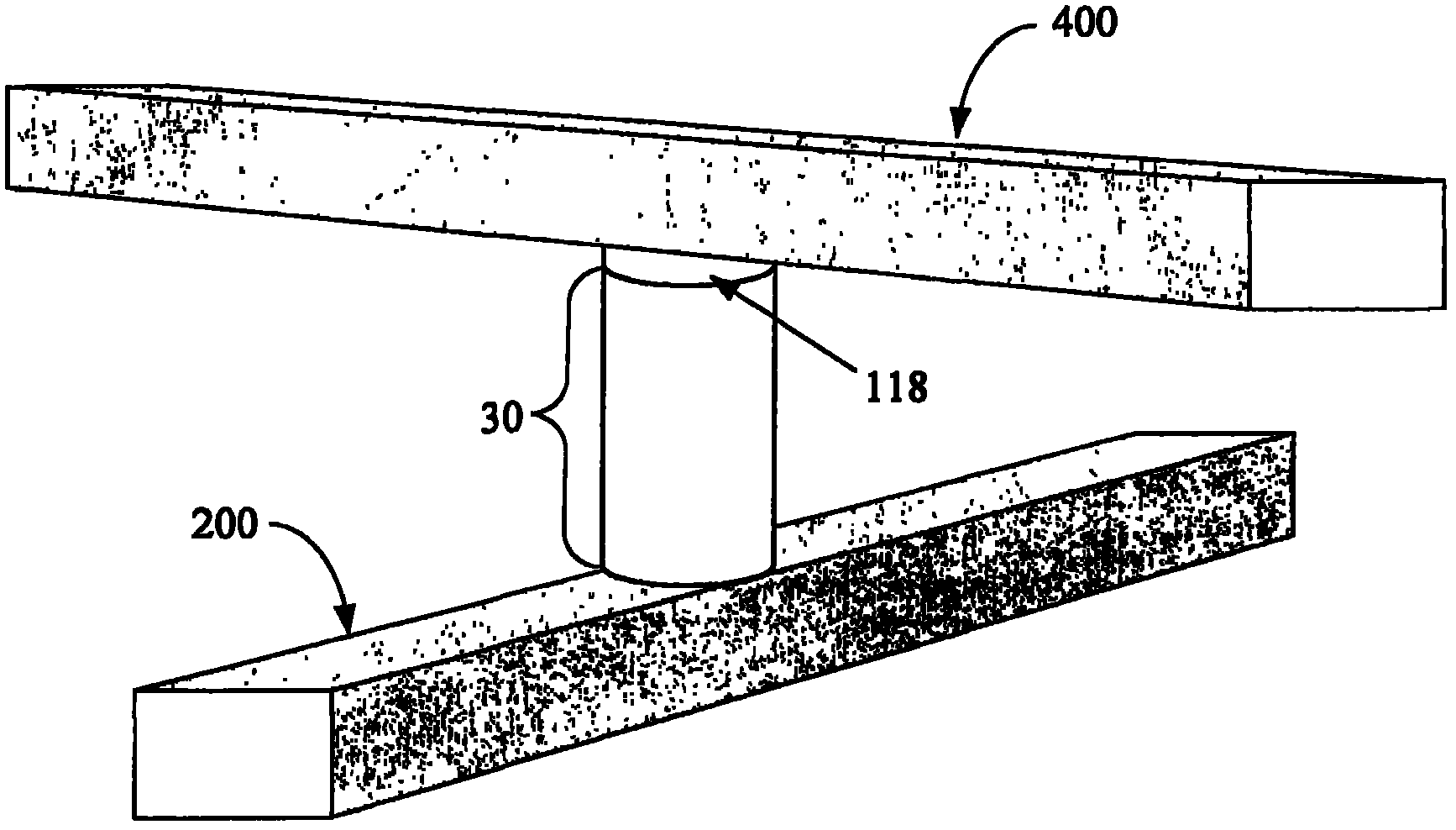
尽管许多实施例是可能的且将描述说明性选择,但图2中展示根据本发明形成的存储器单元的简单型式。所述单元包含底部导体200,其包括导电材料,例如重掺杂半导体材料、导电硅化物或优选为金属,例如钨、铝或铜。形成在此上方的是顶部导体400,其可由与底部导体相同的材料制成。轨道形顶部与底部导体优选地在不同方向上延伸;举例来说,其可为垂直的。所述导体在需要时可包含导电阻挡层或粘合层。设置在顶部导体400与底部导体200之间的是串联布置的二极管30和电阻切换元件118。例如阻挡层等其它层也可包含在导体200与400之间。一旦在电阻切换元件118上施加电压或电流流动,那么电阻切换元件118从低电阻状态转换到高电阻状态,或者从高电阻状态转换到低电阻状态。从低电阻到高电阻的转换是可逆的。A simple version of a memory cell formed in accordance with the present invention is shown in Figure 2, although many embodiments are possible and an illustrative choice will be described. The cell comprises a
二极管30充当单向阀,其在一个方向上比在另一方向上更容易传导电流。在前向方向上的临界“接通”电压以下,二极管30传导少量电流或没有电流。通过使用适当的偏压方案,当选定个别单元进行编程时,相邻单元的二极管可用以电隔离那些单元的电阻切换元件,且因此防止无意编程,只要未选定或半选定单元上的电压不超过在前向方向上施加时的二极管接通电压或在反向方向上施加时的反向击穿电压。
可制造具有居间二极管和电阻切换元件的多个此种顶部和底部导体,从而形成第一存储器层级,图3中展示其一部分。在优选实施例中,可在此第一存储器层级上方堆叠形成额外的存储器层级,从而形成高度密集单片三维存储器阵列。所述存储器阵列由在衬底(例如,单晶硅衬底)上方沉积和生长的层形成。有利的是,在衬底中在存储器阵列下方形成支持电路。A plurality of such top and bottom conductors can be fabricated with intervening diodes and resistive switching elements, forming a first memory level, a portion of which is shown in FIG. 3 . In preferred embodiments, additional memory levels can be stacked above this first memory level to form a highly dense monolithic three-dimensional memory array. The memory array is formed from layers deposited and grown over a substrate (eg, a single crystal silicon substrate). Advantageously, support circuitry is formed in the substrate below the memory array.
一种用于制作可以可靠制造的密集非易失性一次性可编程存储器阵列的有利方法在Herner等人的第10/326,470号美国申请案中教示,由于所述申请案已被放弃,因而下文中将其称为′470申请案,且以引用的方式将其并入本文中。相关的存储器阵列及其使用和制造方法在以下申请案中教示:Herner等人的在2004年9月29日申请且下文中称为′549申请案的题为“Nonvolatile Memory Cell Without a Dielectric Antifuse Having High-and Low-Impedance States”的第10/955,549号美国专利申请案;Herner等人的在2004年12月17日申请且下文中称为′824申请案的题为“Nonvolatile Memory Cell Comprisinga Reduced Height Vertical Diode”的第11/015,824号美国专利申请案;以及Herner等人的在2004年9月29日申请且下文中称为′577申请案的题为“Junction Diode ComprisingVarying Semiconductor Compositions”的第10/954,577号美国专利申请案,所述申请案全部归本申请案的受让人所有,且以引用的方式并入本文中。这些并入的申请案中所教示的方法将可用于制造根据本发明的存储器阵列。An advantageous method for making dense non-volatile one-time programmable memory arrays that can be reliably manufactured is taught in U.S. Application No. 10/326,470 to Herner et al., since said application has been abandoned, the following It is referred to herein as the '470 application and is incorporated herein by reference. Related memory arrays and methods of their use and manufacture are taught in the following application: Herner et al., filed September 29, 2004 and hereinafter referred to as the '549 application, entitled "Nonvolatile Memory Cell Without a Dielectric Antifuse Having High-and Low-Impedance States" U.S. Patent Application No. 10/955,549; Herner et al., filed December 17, 2004 and hereinafter referred to as the '824 application, entitled "Nonvolatile Memory Cell Comprisinga Reduced Height Vertical Diode," U.S. Patent Application No. 11/015,824; and Herner et al., filed September 29, 2004 and hereinafter referred to as the '577 application, entitled "Junction Diode Comprising Varying Semiconductor Compositions" No. 10/ US Patent Application No. 954,577, which is owned in its entirety by the assignee of the present application and is incorporated herein by reference. The methods taught in these incorporated applications will be useful in fabricating memory arrays in accordance with the present invention.
制造选择manufacturing options
优选实施例包含若干种重要变化。一般来说,所选择的电阻率切换材料的属性以及期望使用存储器单元的方式将决定哪些实施例是最有利的。The preferred embodiment incorporates several important variations. In general, the properties of the resistivity-switching material selected and the manner in which the memory cell is expected to be used will determine which embodiments are most beneficial.
非方向性切换与方向性切换:一般来说,指定的电阻切换金属氧化物和氮化物较早地展现两个一般种类的切换特性中的一种。参看图4的I-V曲线,这些材料中的一些初始处于低电阻率状态,在曲线图上的区域A中。电流容易地随施加电压流动,直到达到第一电压V1为止。在电压V1下,电阻率切换材料转换到区域B所示的高电阻率状态,且减少的电流流动。在某一临界较高电压V2下,所述材料切换回到初始低电阻率状态,且增加的电流流动。箭头指示状态改变的次序。此转换是可重复的。对于这些材料,电流流动和电压偏置的方向是不重要的;因此,这些材料将被称为非方向性的。电压V1可被称为复位电压,而电压V2可被称为设定电压。Non-directional vs. directional switching: In general, given resistive switching metal oxides and nitrides exhibit one of two general classes of switching characteristics earlier. Referring to the IV curve of Figure 4, some of these materials are initially in a low resistivity state, in region A on the graph. The current flows easily with the applied voltage until the first voltage V1 is reached. At voltage V 1 , the resistivity-switching material switches to the high-resistivity state shown in region B, and a reduced current flows. At some critical higher voltage V2 , the material switches back to the initial low-resistivity state, and increased current flows. Arrows indicate the sequence of state changes. This transformation is repeatable. For these materials, the direction of current flow and voltage bias is unimportant; therefore, these materials will be referred to as non-directional. Voltage V1 may be referred to as a reset voltage, and voltage V2 may be referred to as a set voltage.
另一方面,所述电阻率切换材料中的其它材料表现如图5a和5b中所示的特性,且将被称为方向性的。方向性电阻率切换材料也可在图5a的区域A所示的低电阻状态中形成。电流容易地随施加电压流动,直到达到第一电压V1(复位电压)为止。在电压V1下,方向性电阻率切换材料转换到图5a的区域B中所示的高电阻率状态。然而,为了将方向性电阻率切换材料转换回低电阻率状态,必须施加反向电压。如图5b所示,方向性电阻率切换材料在负电压下在区域B中是高电阻,直到临界反向电压V2(设定电压)为止。在此电压下,方向性电阻率切换材料回复到低电阻率状态。箭头指示状态改变的次序。(一些材料初始在高电阻率状态中形成。切换特性是相同的;为了简化起见,仅描述了一种初始状态。)On the other hand, the other ones of the resistivity switching materials exhibit properties as shown in Figures 5a and 5b, and will be referred to as directional. Directional resistivity switching materials may also form in the low resistance state shown in region A of Figure 5a. The current easily flows with the applied voltage until reaching the first voltage V 1 (reset voltage). At voltage V1 , the directional resistivity-switching material switches to the high-resistivity state shown in region B of Figure 5a. However, in order to switch the directional resistivity-switching material back to the low-resistivity state, a reverse voltage must be applied. As shown in Figure 5b, the directional resistivity-switching material is high resistivity in region B at negative voltages until a critical reverse voltage V2 (set voltage). At this voltage, the directional resistivity switching material reverts to a low resistivity state. Arrows indicate the sequence of state changes. (Some materials are initially formed in a high-resistivity state. The switching characteristics are identical; for simplicity, only one initial state is depicted.)
在优选实施例中,非方向性电阻率切换材料可与大体上单向性二极管配对。一种此类二极管是图6所示的p-i-n二极管。优选的p-i-n二极管由例如硅等半导体材料形成,且包含具有第一导电类型的底部重掺杂区12、未有意掺杂的中间本征区14以及具有与第一导电类型相反的第二导电类型的顶部重掺杂区16。在图6的p-i-n二极管中,底部区12为n型,而顶部区16为p型;如果需要的话,可颠倒极性。例如区14的本征半导体材料区尽管未被有意掺杂,但将从不呈完全电中性。在许多制造工艺中,本征沉积硅中的缺陷引起此材料表现为似乎略微呈n型。在一些实施例中,可能优选轻掺杂此区。一旦施加电压,此类二极管便表现如图8的I-V曲线所示的特性。在非常低的电压下,少量或没有电流流动。在临界电压V3(二极管的接通电压)下,二极管开始传导,且显著的前向电流流动。当将二极管置于较低且适度的反向电压下(如在图8的区域D中)时,少量或没有电流流动;二极管充当单向阀。In a preferred embodiment, a non-directional resistivity-switching material can be paired with a substantially unidirectional diode. One such diode is the pin diode shown in Figure 6. A preferred pin diode is formed from a semiconductor material such as silicon and includes a bottom heavily doped
然而,一旦施加非常高的反向电压V4,那么二极管将经受雪崩击穿且反向电流将开始流动。此事件可能会破坏二极管,尽管理论上不会破坏。回想到非方向性电阻切换材料的设定电压与复位电压两者均需要仅在一个方向上的电流。因此,图6的p-i-n二极管可成功地与非方向性电阻切换材料配对。However, once a very high reverse voltage V4 is applied, the diode will undergo an avalanche breakdown and a reverse current will start to flow. This event could destroy the diode, although theoretically not. Recall that both the set and reset voltages of non-directional resistance-switching materials require current flow in only one direction. Therefore, the pin diode of FIG. 6 can be successfully paired with non-directional resistance-switching materials.
然而,如图5a和5b的I-V曲线所说明,为了成功切换,方向性电阻率切换材料必须暴露到前向和反向电流两者。图5b所示的低电阻率到高电阻率转换需要反向电流(在电压V2下)。反向电流仅在单向二极管中在反向击穿电压(图8中的电压V4)下实现,所述反向击穿电压通常相对较高,例如至少9伏。However, as illustrated by the IV curves of Figures 5a and 5b, for successful switching, a directional resistivity switching material must be exposed to both forward and reverse current flow. The low-resistivity to high-resistivity transition shown in Figure 5b requires a reverse current (at voltage V2 ). Reverse current flow is only achieved in unidirectional diodes at a reverse breakdown voltage (voltage V 4 in FIG. 8 ), which is usually relatively high, eg at least 9 volts.
因此,方向性电阻率切换材料可能不会有利地与单向二极管配对。而是,此类材料可与可逆非欧姆装置(即,允许电流在任一方向上流动的装置)配对。一种此类装置为Zener二极管。图7展示示范性Zener二极管。将看到,此类二极管具有具第一导电类型的第一重掺杂区12以及具相反导电类型的第二重掺杂区16。极性可以颠倒。图7的Zener二极管中没有本征区;在一些实施例中,可能存在非常薄的本征区。图9展示Zener二极管的I-V曲线。Zener二极管在前向偏压下在接通电压V3处表现为类似于p-i-n二极管。然而,在反向偏压下,一旦达到临界电压V4,Zener二极管就将允许反向电流流动。在Zener二极管中,临界反向电压V4在量值上大体上低于单向二极管的临界反向电压。需要此种在适度电压下的可控反向电流来将方向性电阻率切换材料从高电阻率状态转换到低电阻率状态,如早先描述和图5b所示的(在电压V2下)。因此,在使用方向性电阻率切换材料的本发明实施例中,Zener二极管是优选的。(事实上,具有极小本征区的p-i-n二极管与Zener二极管之间的差别是人为的,但常规上由所属领域的技术人员做出。)Therefore, directional resistivity switching materials may not pair favorably with unidirectional diodes. Rather, such materials can be paired with reversible non-ohmic devices (ie, devices that allow electrical current to flow in either direction). One such device is a Zener diode. Figure 7 shows an exemplary Zener diode. It will be seen that such a diode has a first heavily doped
非方向性材料在前向和反向方向上均不需要电流,但如所描述的,可在任一方向上实现电阻率切换。于是,对于一些电路布置,可能有利的是将非方向性电阻率切换材料与Zener二极管配对。Non-directional materials require no current flow in both the forward and reverse directions, but resistivity switching can be achieved in either direction as described. Thus, for some circuit arrangements it may be advantageous to pair a non-directional resistivity-switching material with a Zener diode.
本文中使用术语“结二极管”来指代具有非欧姆传导属性、具有两个端电极且由在一个电极处为p型且在另一电极处为n型的半传导材料制成的半导体装置。实例包含:p-n二极管和n-p二极管,其具有接触的p型半导体材料和n型半导体材料,例如Zener二极管;以及p-i-n二极管,其中本征(未掺杂)半导体材料插入在p型半导体材料与n型半导体材料之间。The term "junction diode" is used herein to refer to a semiconductor device having non-ohmic conducting properties, having two terminal electrodes, and made of a semiconducting material that is p-type at one electrode and n-type at the other electrode. Examples include: p-n diodes and n-p diodes, which have contacting p-type semiconductor material and n-type semiconductor material, such as Zener diodes; and p-i-n diodes, where intrinsic (undoped) semiconductor material is inserted between p-type semiconductor material and n-type semiconductor material. between semiconductor materials.
高电流要求:为复位电阻率切换材料,从而造成非方向性电阻率切换材料中从高电阻率状态向低电阻率状态转变,对于一些材料来说可能需要相对较高的电流。对于这些材料,二极管可优选地为锗或锗合金,其在给定电压下与硅相比提供较高的电流。High current requirements: Relatively high currents may be required for some materials to reset a resistivity switching material, thereby causing a transition from a high resistivity state to a low resistivity state in non-directional resistivity switching materials. For these materials, the diode may preferably be germanium or a germanium alloy, which provides a higher current at a given voltage than silicon.
贵金属接点和低温制造:已观察到,当电阻率切换材料夹在可例如由Ir、Pt、Pd或Au形成的贵金属接点之间时,更容易且可靠地实现早先提到的金属氧化物与氮化物中的一些的电阻率切换。图10展示其中使用贵金属接点的根据本发明的单元的实例。电阻率切换元件118在贵金属层117与119之间。Noble Metal Junctions and Low Temperature Fabrication: It has been observed that the earlier mentioned metal oxide and nitrogen Resistivity switching of some of the compounds. Figure 10 shows an example of a cell according to the invention in which noble metal contacts are used. The
然而,使用贵金属提出了挑战。当暴露于高温时,贵金属往往会快速扩散,且可损坏装置的其它部分。举例来说,在图10中,贵金属层117邻近于半导体二极管30。贵金属广泛扩散到二极管30的半导体材料中将损害装置性能。于是,当在贵金属接点之间形成电阻率切换元件时,有利的是使处理温度达到最小。二极管可以是硅、锗或硅锗合金。锗与硅相比可在较低温度下结晶,且随着硅锗合金的锗含量增加,结晶温度减小。当使用贵金属接点时,由锗或锗合金形成的二极管可为优选的。However, using precious metals presents challenges. Precious metals tend to diffuse rapidly when exposed to high temperatures and can damage other parts of the device. For example, in FIG. 10 , the
多结晶硅(在此论述内容中,多结晶硅将被称为多晶硅,而多结晶锗将被称为多晶锗)的常规沉积和结晶温度相对较高,从而放弃使用以常规方式形成的与某些具有相对较低熔点的金属不相容的多晶硅二极管。举例来说,当暴露于高于大约475摄氏度的温度时,铝线开始软化并挤出。出于此原因,在′470、′549和′824申请案的许多实施例中,优选的是在导体中使用钨,因为钨布线可承受较高温度。然而,如果使用锗或锗合金,那么锗的较低沉积和结晶温度可允许在导体中(例如,在图10的导体200和400中)使用铝或甚至铜。这些金属具有低薄层电阻,且因此在热学预算允许其使用的情况下通常是优选的,但可改为使用钨或某种其它导电材料。当低温为优选的时,涉及低温制造的以引用方式并入本文中的Herner等人的题为“High-Density Nonvolatile Memory ArrayFabricated at Low Temperature Comprising Semiconductor Diodes”的第11/125,606号美国专利申请案的任何教示均可适用。The conventional deposition and crystallization temperatures of polycrystalline silicon (in the context of this discussion, polycrystalline silicon will be referred to as polycrystalline silicon and polycrystalline germanium polycrystalline germanium) are relatively high, thereby forgoing the use of conventionally formed and Certain metals with relatively low melting points are not compatible with polysilicon diodes. For example, when exposed to temperatures above about 475 degrees Celsius, aluminum wire begins to soften and extrude. For this reason, in many embodiments of the '470, '549, and '824 applications, it is preferred to use tungsten in the conductors because tungsten wiring can withstand higher temperatures. However, the lower deposition and crystallization temperature of germanium may allow the use of aluminum or even copper in conductors (eg, in
导电和隔离:已经描述到,为了能够在大阵列中编程,在每一存储器单元中包含二极管以提供相邻单元之间的电隔离。一些电阻率切换材料在高电阻率状态中沉积,而其它材料在低电阻率状态中沉积。对于在高电阻率状态中沉积的电阻率切换材料,一般来说,转换到低电阻率状态是局部化现象。举例来说,参看图11a,假设存储器单元(以横截面展示)包含从左向右延伸穿过页面的轨道形底部导体200、二极管30、在高电阻率状态中形成的电阻率切换材料层118以及延伸出页面的轨道形顶部导体400。在此情况下,电阻率切换材料层118已经形成为覆盖层。只要电阻率切换材料层118的高电阻率状态充分高,层118就将不会提供不合意的将导体400短路到邻近导体或将二极管30短路到邻近二极管的导电路径。当电阻率切换材料层118暴露于高电压且转换到低电阻率状态时,预期只有层118的紧邻二极管的区域将进行转换;举例来说,在编程之后,层118的阴影区将为低电阻率,而无阴影区将保持高电阻率。所述阴影区是设置在电阻率切换材料连续层118内的电阻率切换元件。Conduction and Isolation: It has been described that to enable programming in large arrays, a diode is included in each memory cell to provide electrical isolation between adjacent cells. Some resistivity-switching materials are deposited in the high-resistivity state, while other materials are deposited in the low-resistivity state. For resistivity-switching materials deposited in the high-resistivity state, in general, the transition to the low-resistivity state is a localized phenomenon. For example, referring to Figure 11a, assume a memory cell (shown in cross-section) comprising a track-shaped
然而,依据读取、设定和复位电压而定,对于一些电阻率切换材料,电阻率切换材料的高电阻率状态对于可靠隔离来说可能过于导电,且在形成为如图11a的连续层时将往往会短路邻近导体或二极管。于是,对于不同的电阻率切换材料,可合意地提供a)保持电阻率切换材料118未图案化,如在图11a的装置中,或b)用顶部或底部导体图案化电阻率切换材料118,如在图11b(透视图)的装置中,或c)用二极管30图案化电阻率切换材料118,如在图2和10的装置中。However, depending on the read, set, and reset voltages, for some resistivity-switching materials, the high-resistivity state of the resistivity-switching material may be too conductive for reliable isolation, and when formed as a continuous layer as in Figure 11a will tend to short out adjacent conductors or diodes. Thus, for different resistivity-switching materials, it may be desirable to provide either a) leaving the resistivity-switching
当存储器元件由在低电阻率状态中形成的电阻率切换材料形成时,其必须与邻近单元的电阻率切换存储器元件隔离,以避免在其之间形成不希望的导电路径。When a memory element is formed from a resistivity-switching material that is formed in a low-resistivity state, it must be isolated from the resistivity-switching memory element of an adjacent cell to avoid forming an undesired conductive path therebetween.
如′549申请案中以及下文称为′530申请案且以引用方式并入本文中的Herner等人2005年6月8日申请的题为“Nonvolatile Memory Cell Operating by Increasing Order inPolycrystalline Semiconductor Material”的第11/148,530号美国专利申请案中详细描述的,对于根据其中详细描述的方法而形成的多晶半导体二极管,可预期在一些实施例中,二极管的多晶体将在初始高电阻率状态中形成,且一旦施加充分高的电压,就将永久转换为低电阻率状态。因此,参看图2的单元,当此单元初始形成时,二极管30的多晶硅与可逆电阻切换元件118两者均在高电阻率状态中形成。As in the '549 application and hereafter referred to as the '530 application and incorporated herein by reference, Herner et al., filed June 8, 2005, entitled "Nonvolatile Memory Cell Operating by Increasing Order in Polycrystalline Semiconductor Material" As detailed in U.S. Patent Application No. 11/148,530, for polycrystalline semiconductor diodes formed according to the methods detailed therein, it is contemplated that in some embodiments the polycrystal of the diode will form in an initial high-resistivity state, And once a sufficiently high voltage is applied, it will permanently switch to a low-resistivity state. Thus, referring to the cell of FIG. 2, both the polysilicon of
一旦第一次施加编程电压,二极管30的多晶硅与电阻率切换元件118两者均将转换为其低电阻率状态。一般来说,二极管30的转换是永久的,而电阻率切换元件118的转换是可逆的。可能需要在工厂条件下执行二极管的多晶硅从高电阻率到低电阻率的初始转换,从而有效地“预调节”所述二极管。Once the programming voltage is first applied, both the polysilicon of
作为替代,下文称为′510申请案并转让给本发明受让人且以引用方式并入本文中的Herner在2004年9月29日申请的题为“Memory Cell Comprising a Semiconductor JunctionDiode Crystallized Adiacent to a Silicide”的第10/954,510号美国专利申请案描述了一种用以形成多晶半导体二极管的方法,所述多晶半导体二极管在形成时处于低电阻率状态中。在′510申请案的优选实施例中,二极管的半导体材料(通常为硅)在邻近于硅化物层(例如,TiSi2)处结晶。所述硅化物层在硅结晶时为硅提供有序结晶模板,从而在形成时产生具有较少结晶缺陷的高度结晶二极管。本发明中可使用此技术。如果二极管为锗,那么锗二极管在邻近于锗化物层(例如TiGe2)处结晶,这将为锗提供类似的结晶模板。此类二极管的锗在形成时将为低电阻率,而不需要“编程”步骤来创建穿过其的低电阻路径。Instead, Herner, hereinafter referred to as the '510 application and assigned to the assignee of the present invention and incorporated herein by reference, filed September 29, 2004, entitled "Memory Cell Comprising a Semiconductor Junction Diode Crystallized Adiacent to a US Patent Application No. 10/954,510 to "Silicide" describes a method for forming polycrystalline semiconductor diodes that are in a low-resistivity state as formed. In a preferred embodiment of the '510 application, the semiconductor material of the diode (typically silicon) is crystallized adjacent to the silicide layer (eg, TiSi2 ). The silicide layer provides an ordered crystalline template for the silicon as it crystallizes, resulting in a highly crystalline diode with fewer crystalline defects when formed. This technique can be used in the present invention. If the diode is germanium, the germanium diode is crystallized adjacent to the germanide layer (eg TiGe2 ), which will provide a similar crystallization template for germanium. The germanium of such a diode will be low resistivity when formed, without the need for a "programming" step to create a low resistance path through it.
一次性可编程存储器单元:两个状态One-Time Programmable Memory Cell: Two States
当用作可重写存储器单元时,本发明实施例中已经描述了与电阻切换元件配对的二极管。这些元件也可在替代实施例中用以形成一次性可编程存储器单元。Diodes paired with resistive switching elements have been described in embodiments of the present invention when used as rewritable memory cells. These elements may also be used in alternative embodiments to form one-time programmable memory cells.
对于氧化镍或可在较低电阻率状态与较高电阻率状态之间切换的指定电阻率切换二元金属氧化物或氮化物中的任一者来说,从较低电阻率状态向较高电阻率状态的复位切换可证明为较困难的切换。(将了解,在此论述内容中“氧化镍”可指代定比NiO或非定比化合物。)尽管实际的切换机制不清楚,但似乎必须在电阻率切换层上施加某一电压以致使其切换。如果材料的设定状态为极低电阻率,且所述材料高度导电,那么可能难以建立充足电压以致使发生切换。通过使用本发明的存储器单元作为一次性可编程单元,可避免较困难的切换。这通常简化了编程电路。For either nickel oxide or a specified resistivity-switching binary metal oxide or nitride switchable between a lower-resistivity state and a higher-resistivity state, the transition from the lower-resistivity state to the higher-resistivity state is The reset switch of the resistivity state can prove to be a difficult switch. (It will be appreciated that in the context of this discussion "nickel oxide" may refer to either a ratiometric NiO or a non-stoichiometric compound.) Although the actual switching mechanism is unclear, it appears that a certain voltage must be applied across the resistivity-switching layer to cause it to switch. If the set state of the material is very low resistivity, and the material is highly conductive, it may be difficult to build up sufficient voltage to cause switching to occur. By using the memory cells of the present invention as one-time programmable cells, more difficult switching can be avoided. This generally simplifies programming the circuit.
一种优选的电阻率切换材料(氧化镍)是非方向性的,这意味着所述材料通过所施加的正电压或负电压单独切换。但在一些实施例中已经发现,当与二极管配对时,通过在反向偏压下的二极管最容易实现氧化镍层的复位。在衬底中可能需要额外晶体管来提供负电压以反向偏置二极管。这些晶体管消耗衬底空间,从而使装置较昂贵,且形成这些晶体管可能增加工艺复杂性。因此,在需要反向偏压进行复位的实施例中,使用单元作为一次写入单元并避免复位避免了产生负电压的难题。A preferred resistivity switching material (nickel oxide) is non-directional, which means that the material is switched independently by an applied positive or negative voltage. However, it has been found in some embodiments that when paired with a diode, reset of the nickel oxide layer is most easily achieved by the diode under reverse bias. An additional transistor may be required in the substrate to provide a negative voltage to reverse bias the diode. These transistors consume substrate space, making the device more expensive, and forming them can add process complexity. Thus, in embodiments that require a reverse bias for reset, using the cell as a write-once cell and avoiding reset avoids the difficulty of creating negative voltages.
在使用根据本发明的包括二极管和电阻率切换层的存储器单元作为一次性可编程存储器单元的最简单方法中,所述单元具有两个值——未编程和已编程,其对应于通过所述单元的两个相异读取电流。In the simplest method of using a memory cell comprising a diode and a resistivity-switching layer according to the invention as a one-time programmable memory cell, the cell has two values - unprogrammed and programmed, which correspond to the Two distinct read currents for the cell.
设定电压将依据用于电阻切换元件的材料、层厚度、材料特性和其它因素而变化。增加脉冲时间可减小将材料从高电阻设定到低电阻所需的电压。设定电压可从(例如)4伏变化到10伏。The set voltage will vary depending on the material used for the resistive switching element, layer thickness, material properties, and other factors. Increasing the pulse time reduces the voltage required to set the material from high resistance to low resistance. The set voltage can vary from, for example, 4 volts to 10 volts.
如早先描述的,如果二极管由多晶硅形成,那么在邻近于具有位于为硅提供良好结晶模板的定向处的晶格结构的硅化物处结晶多晶硅将产生较低缺陷且较低电阻率的多晶硅;而在仅邻近于具有弱晶格匹配的材料(例如氮化钛)处结晶将产生较高缺陷且较高电阻率的多晶硅。如果二极管由较高电阻多晶硅形成,那么需要在二极管上施加合适的编程电压以将多晶硅转换为低电阻率状态,从而使二极管具有良好的整流特性。As described earlier, if the diode is formed from polysilicon, then crystallizing the polysilicon adjacent to the silicide with a lattice structure located in an orientation that provides a good crystallization template for the silicon will result in lower defect and lower resistivity polysilicon; and Crystallization only adjacent to materials with a weak lattice match, such as titanium nitride, will result in higher defect and higher resistivity polysilicon. If the diode is formed from higher resistance polysilicon, then a suitable programming voltage needs to be applied across the diode to convert the polysilicon to a low resistivity state so that the diode has good rectifying characteristics.
此外,已经发现,对于某些在初始高电阻率状态中形成的电阻率切换金属氧化物或氮化物,在一些实施例中,可能需要形成脉冲来实现从高电阻率到低电阻率的第一切换。此形成脉冲与随后的低到高或高到低电阻率切换相比可能需要较高的电压。举例来说,在一个实验中,所述形成脉冲约为8.5到9伏,而随后的设定脉冲约为6.5到7伏。Additionally, it has been found that for certain resistivity-switching metal oxides or nitrides formed in the initial high-resistivity state, in some embodiments, pulsing may be required to achieve the first transition from high-resistivity to low-resistivity. switch. This forming pulse may require a higher voltage than the subsequent low-to-high or high-to-low resistivity switching. For example, in one experiment, the forming pulse was about 8.5 to 9 volts, and the subsequent setting pulse was about 6.5 to 7 volts.
如下文称为′452申请案且以引用方式并入本文中的Herner等人2005年11月23日申请的题为“Reversible Resistivity-Switching Metal Oxide or Nitride Layer with addedMetal”的第11/287,452号美国专利申请案中描述的,向二元金属氧化物或氮化物添加金属可减小设定和复位电压,且可减小形成脉冲的幅值或完全消除对形成脉冲的需要。一般来说,金属添加剂处于金属氧化物或氮化物化合物层中的金属原子的约0.01%与约5%之间。用于金属添加剂的优选金属选自由以下金属组成的群组:钴、铝、镓、铟、锰、镍、铌、锆、钛、铪、钽、镁、铬、钒、硼、钇和镧。U.S. Ser. No. 11/287,452, entitled "Reversible Resistivity-Switching Metal Oxide or Nitride Layer with added Metal," filed November 23, 2005, Herner et al., hereinafter referred to as the '452 application and incorporated herein by reference. As described in the patent application, adding metal to binary metal oxides or nitrides can reduce set and reset voltages, and can reduce the amplitude of the forming pulses or eliminate the need for forming pulses entirely. Generally, the metal additive is between about 0.01% and about 5% of the metal atoms in the metal oxide or nitride compound layer. Preferred metals for metal additives are selected from the group consisting of cobalt, aluminum, gallium, indium, manganese, nickel, niobium, zirconium, titanium, hafnium, tantalum, magnesium, chromium, vanadium, boron, yttrium and lanthanum.
因此,对于包含二元金属氧化物或氮化物电阻切换元件和二极管的一次性可编程存储器单元来说,许多选择是可能的。应考虑将电阻切换元件与具有高电阻率或低电阻率多晶硅的二极管配对的效果。Thus, many options are possible for a one-time programmable memory cell comprising a binary metal oxide or nitride resistive switching element and a diode. The effect of pairing a resistance-switching element with a diode with high-resistivity or low-resistivity polysilicon should be considered.
如果所述二元金属氧化物或氮化物在高电阻率状态中形成且所述二极管由低缺陷且低电阻率多晶硅形成,那么通过将二元金属氧化物或氮化物转换到设定状态来实现存储器单元向已编程状态的转换,其中高电流在读取电压下流动。然而,如果所述二极管由高缺陷且高电阻率多晶硅形成,那么二极管的多晶硅必须同样经历用于存储器单元的编程电压以表现为似乎已编程,从而允许高电流在所施加读取电压下流动。If the binary metal oxide or nitride is formed in a high resistivity state and the diode is formed from low defect and low resistivity polysilicon, then by switching the binary metal oxide or nitride to a set state The transition of a memory cell to a programmed state in which a high current flows at a read voltage. However, if the diode is formed from highly defective and high resistivity polysilicon, the polysilicon of the diode must also experience the programming voltage for the memory cell to appear programmed, allowing high current to flow at the applied read voltage.
依据引起多晶硅的无序到有序转换以及二元金属氧化物或氮化物的高到低电阻率转换所需的相对电压,可优选使用低缺陷多晶硅二极管,其中多晶硅在邻近于适当的硅化物处结晶。Depending on the relative voltages required to induce disorder-to-order transitions in polysilicon and high-to-low-resistivity transitions in binary metal oxides or nitrides, it may be preferable to use low-defect polysilicon diodes where the polysilicon is adjacent to the appropriate silicide crystallization.
如果对于在高电阻率状态中形成的二元金属氧化物或氮化物需要较大形成脉冲,那么另一替代方案是在工厂中在预调节步骤中施加形成脉冲。形成脉冲所需的高电压可从电路小片外部供应,且因此无需在电路小片上可用。如果需要反向偏压进行复位,那么也可在进一步预调节步骤中施加复位脉冲,因此当存储器阵列为最终用户准备好时,单元处于复位状态,且可通过较低的后形成设定电压来编程。以此方式,电路小片上的电路无需提供高电压形成脉冲或负电压,从而简化了电路要求。Another alternative is to apply the forming pulses at the factory in a preconditioning step if a larger forming pulse is required for the binary metal oxide or nitride formed in the high resistivity state. The high voltages required to form the pulses can be supplied externally from the die, and therefore need not be available on the die. If reverse bias is required for reset, the reset pulse can also be applied in a further pre-conditioning step, so when the memory array is ready for the end user, the cells are in reset and can be reset by a lower post-formation set voltage programming. In this way, the circuitry on the die does not need to provide high voltage forming pulses or negative voltages, simplifying circuit requirements.
此外,如果在工厂中施加预调节形成脉冲和复位脉冲,那么对于形成脉冲所需的较大电压可能足以将二极管的高缺陷多晶硅从高电阻率转换到低电阻率。在此情况下,对于使用非硅化高缺陷二极管没有缺点,且可避免提供硅化物模板层的额外工艺复杂性。Furthermore, if preconditioning forming pulses and reset pulses are applied in the factory, the larger voltage required for the forming pulses may be sufficient to switch the diode's highly defective polysilicon from high resistivity to low resistivity. In this case, there is no disadvantage to using non-silicided high-defect diodes, and the additional process complexity of providing a suicide template layer can be avoided.
通过这样一种方法对在存储器阵列中的此类存储器单元进行编程(其中所述存储器单元包括金属氧化物或氮化物化合物的电阻率切换层,所述金属氧化物或氮化物化合物恰好包含一种金属),所述方法包括:通过将所述电阻率切换层从第一电阻率状态改变为第二编程电阻率状态来编程存储器单元,其中所述第二编程电阻率状态存储所述存储器单元的数据状态。所述存储器阵列包括用以编程和读取存储器单元的电路,且所述电路适于对存储器单元编程仅仅一次。所述存储器阵列为一次性可编程阵列。Such memory cells in memory arrays are programmed by a method in which the memory cells comprise a resistivity-switching layer of a metal oxide or nitride compound containing exactly one metal), the method comprising: programming a memory cell by changing the resistivity switching layer from a first resistivity state to a second programmed resistivity state, wherein the second programmed resistivity state stores the memory cell's data status. The memory array includes circuitry to program and read memory cells, and the circuitry is adapted to program memory cells only once. The memory array is a one-time programmable array.
一次性可编程,多个状态One-time programmable, multiple states
在另一实施例中,可实际上优选将二元金属氧化物或氮化物与由高缺陷多晶硅形成的二极管配对。构成二极管的多晶硅的两个状态(即,初始高电阻率状态以及已编程低电阻率状态)可用于存储数据,从而增加存储器单元的密度。In another embodiment, it may actually be preferable to pair a binary metal oxide or nitride with a diode formed from high defect polysilicon. The two states of polysilicon that make up the diode (ie, the initial high-resistivity state and the programmed low-resistivity state) can be used to store data, thereby increasing the density of memory cells.
举例来说,假设由高缺陷多晶硅(不在邻近于适当硅化物处结晶)形成的二极管与氧化镍层配对,所述两者以电学方式串联布置在顶部导体与底部导体之间。氧化镍在高电阻率状态中形成,从而需要形成脉冲来实现从高电阻率向低电阻率的第一转换。假设二极管需要8伏的编程电压来引起′530申请案中描述的无序到有序转换,从而将多晶硅转换为较高电阻率状态。进一步假设氧化镍所需的用于形成脉冲的电压为10伏。(将了解,这里给出的电压仅为实例。电压将随着装置特性和其它因素变化而改变。)For example, assume a diode formed of high defect polysilicon (not crystallized adjacent to the appropriate silicide) is paired with a layer of nickel oxide, the two arranged electrically in series between the top and bottom conductors. Nickel oxide forms in the high-resistivity state, requiring a pulse to achieve the first transition from high-resistivity to low-resistivity. Assume that the diode requires a programming voltage of 8 volts to cause the disorder-to-order transition described in the '530 application, thereby converting the polysilicon to a higher resistivity state. Assume further that the voltage required for the nickel oxide to form the pulse is 10 volts. (It will be appreciated that the voltages given here are examples only. Voltages will vary with device characteristics and other factors.)
所形成的存储器单元具有高电阻率氧化镍和高电阻率多晶硅二极管。以下表1概述此存储器单元可实现的三种数据状态。对于此实例,其还包含获得每一状态所需的编程以及针对所施加+2伏读取电压下的每一数据状态所预期的实例性读取电流:The formed memory cells have high resistivity nickel oxide and high resistivity polysilicon diodes. Table 1 below summarizes the three data states achievable by this memory cell. For this example, it also includes the programming required to obtain each state and the example read current expected for each data state at the applied +2 volt read voltage:
表1Table 1
在未施加编程电压的情况下,所形成的存储器单元处于第一数据状态,所述第一数据状态出于方便起见将被称为‘00’状态。施加+8伏足以将二极管的多晶硅从高电阻率转换到低电阻率,但低于形成脉冲所需的电压,从而使氧化镍保留在其初始高电阻率状态;此数据状态将被称为‘10’。向初始‘00’状态中的单元施加+11伏足以实现多晶硅的无序到有序转换,且足以将氧化镍设定为低电阻率状态。此数据状态将被称为‘11’状态。With no programming voltage applied, the formed memory cells are in a first data state, which for convenience will be referred to as the '00' state. The application of +8 volts is sufficient to switch the polysilicon of the diode from high resistivity to low resistivity, but below the voltage required to form the pulse so that the nickel oxide remains in its initial high resistivity state; this data state will be referred to as the ' 10'. Application of +11 volts to the cell in the initial '00' state was sufficient to effect a disorder-to-order transition of the polysilicon, and sufficient to set the nickel oxide into a low-resistivity state. This data state will be referred to as the '11' state.
在另一实施例中,可能不需要形成脉冲或仅需要较小形成脉冲,且设定电压可能小于切换多晶硅所需的电压。在此情况下,在表2中概述可实现的数据状态:In another embodiment, no formation pulses or only smaller formation pulses may be required, and the set voltage may be less than that required to switch polysilicon. In this case, the achievable data states are summarized in Table 2:
表2Table 2
在形成时,存储器单元处于‘00’状态,其中多晶硅和氧化镍两者均为高电阻率。施加+6伏设定氧化镍,但不足以切换多晶硅,从而使单元保留在‘01’状态。施加8伏切换多晶硅和氧化镍两者,从而使两者保留在低电阻率状态,这对应于‘11’数据状态。As formed, the memory cell is in the '00' state, where both polysilicon and nickel oxide are high resistivity. Applying +6 volts sets the NiO, but not enough to switch the polysilicon, leaving the cell in the '01' state. Application of 8 volts switches both polysilicon and nickel oxide, leaving both in the low resistivity state, which corresponds to the '11' data state.
在这些实施例的任一者中,一旦单元处于‘11’状态,那么可通过复位氧化镍来实现第四数据状态,其中二极管的多晶硅处于低电阻率状态且氧化镍处于复位状态。此状态将被称为‘10’状态,且在需要反向偏压进行复位的实施例中,通过向处于‘11’状态的单元施加负复位脉冲(比如,-4伏)来实现此状态。In either of these embodiments, once the cell is in the '11' state, the fourth data state can be achieved by resetting the nickel oxide, with the polysilicon of the diode in the low resistivity state and the nickel oxide in the reset state. This state will be referred to as the '10' state, and is achieved by applying a negative reset pulse (eg, -4 volts) to a cell in the '11' state in embodiments that require a reverse bias for reset.
概括地说,通过这样一种方法对刚才描述的存储器单元进行编程,所述方法包括i)向存储器单元施加第一编程脉冲,其中所述第一编程脉冲:a)可检测地改变电阻率切换层的第一电阻率状态;或b)可检测地改变多晶半导体材料的第二电阻率状态,或c)可检测地改变电阻率切换层的第一电阻率状态并可检测地改变多晶半导体材料的第二电阻率状态;以及ii)读取存储器单元,其中电阻率切换层的第一电阻率状态用以存储数据且多晶半导体材料的第二电阻率状态用以存储数据。所述存储器单元适于存储三种或四种数据状态中的一种。In summary, the memory cell just described is programmed by a method comprising i) applying a first programming pulse to the memory cell, wherein the first programming pulse: a) detectably changes the resistivity switch the first resistivity state of the layer; or b) detectably alter the second resistivity state of the polycrystalline semiconductor material, or c) detectably alter the first resistivity state of the resistivity switching layer and detectably alter the polycrystalline the second resistivity state of the semiconductor material; and ii) reading the memory cell, wherein the first resistivity state of the resistivity switching layer is used to store data and the second resistivity state of the polycrystalline semiconductor material is used to store data. The memory cells are adapted to store one of three or four data states.
多个电阻级别Multiple Resistance Levels
本文中提到的电阻率切换二元氧化物或氮化物能够获得两种以上稳定的电阻率状态。于是,在一些实施例中,根据本发明形成的阵列的存储器单元能够通过将金属氧化物或氮化物置于三种、四种或更多可检测相异电阻率状态中的一者来存储两种以上数据状态,例如三种、四种或更多数据状态。可通过感测和解码阵列中的电路来可靠地检测可检测相异数据状态。这些实施例可以是可重写的或一次性可编程的。The resistivity-switching binary oxides or nitrides mentioned in this paper can obtain more than two stable resistivity states. Thus, in some embodiments, memory cells of arrays formed in accordance with the present invention are capable of storing two More than one data state, such as three, four or more data states. Detectable distinct data states can be reliably detected by sensing and decoding circuitry in the array. These embodiments may be rewritable or one-time programmable.
举例来说,假设电阻率切换金属氧化物或氮化物为氧化镍(将了解,可使用任何其它指定材料),所述氧化镍已经在高电阻率状态中形成。转向图12,在形成时,氧化镍处于标记为00的曲线上所展示的最低电阻率状态中。For example, assume that the resistivity-switching metal oxide or nitride is nickel oxide (it will be understood that any other specified material may be used), which has been formed in the high-resistivity state. Turning to Figure 12, as formed, nickel oxide is in its lowest resistivity state shown on the curve labeled 00.
可将氧化镍置于两种以上可检测相异电阻率状态中。举例来说,类似图2所示存储器单元的存储器单元可具有四种不同状态,每一种状态可通过在例如约2伏的施加读取电压下的电流流动范围来区别。Nickel oxide can be placed in more than two detectably different resistivity states. For example, a memory cell like that shown in FIG. 2 can have four different states, each state distinguishable by a range of current flow at an applied read voltage of, for example, about 2 volts.
在此实例中,在最高电阻率状态中,当在存储器单元上施加2伏时小于约30毫微安的电流流动;这将被称为‘00’状态。在‘01’状态中,在2伏下,电流将处于约100与300毫微安之间。在‘10’状态中,在2伏下,电流将处于约1微安与3微安之间。在最低电阻率状态(‘11’状态)中,2伏下的电流将大于9微安。将了解,仅为了清楚起见供应这些电流范围和读取电压;依据所使用的实际材料和装置特征而定,其它值可能是适当的。In this example, in the highest resistivity state, less than about 30 nanoamperes of current flow when 2 volts are applied across the memory cell; this will be referred to as the '00' state. In the '01' state, at 2 volts, the current will be between about 100 and 300 nanoamperes. In the '10' state, at 2 volts, the current will be between about 1 microampere and 3 microamperes. In the lowest resistivity state (the '11' state), the current at 2 volts will be greater than 9 microamps. It will be appreciated that these current ranges and read voltages are given for clarity only; other values may be appropriate depending on the actual materials and device characteristics used.
在此实例中,设定脉冲具有在约8伏与约10伏之间的电压,而复位电压处于约3伏与约6伏之间。在包含与p-i-n二极管配对的氧化镍的实施例中,以反向偏压施加复位电压。但依据所使用的材料以及存储器单元的配置和特征而定,可能不需要反向偏压来复位单元。In this example, the set pulse has a voltage between about 8 volts and about 10 volts, while the reset voltage is between about 3 volts and about 6 volts. In embodiments comprising nickel oxide paired with p-i-n diodes, the reset voltage is applied with reverse bias. But depending on the materials used and the configuration and characteristics of the memory cell, a reverse bias may not be required to reset the cell.
参看图12,单元在‘00’状态中形成。为了将单元编程为01状态,可施加(例如)8伏的设定电压。对于所有设定脉冲,电路中优选包含电流限制器。在施加设定脉冲之后,在2伏下读取单元。如果2伏下的电流处于‘01’状态的预期范围内(在约100与约300毫微安之间),那么将单元视为待编程。如果电流过低(例如,80毫微安),那么施加视情况处于较高设定电压的额外设定脉冲,且再次在2伏下读取单元。重复所述过程,直到通过存储器单元的电流在2伏下处于正确范围内。Referring to Figure 12, cells are formed in the '00' state. To program a cell to the 01 state, a set voltage of, for example, 8 volts may be applied. For all set pulses, a current limiter is preferably included in the circuit. Cells were read at 2 volts after application of the set pulse. If the current at 2 volts is within the expected range for the '01 ' state (between about 100 and about 300 nanoamperes), then the cell is considered to be programmed. If the current is too low (eg, 80 nanoamperes), then an additional set pulse is applied, optionally at a higher set voltage, and the cell is again read at 2 volts. The process is repeated until the current through the memory cell is in the correct range at 2 volts.
在施加编程脉冲之后,电流可改为高于‘01’状态的可接受范围;举例来说,其可为400毫微安。在此情况下存在两种选择:可施加足以使氧化镍返回‘00’状态的复位脉冲,随后是另一可能较小的设定脉冲;或可施加复位脉冲以略微增加氧化镍层的电阻率,从而将其以递增方式移动到‘01’范围内。重复所述过程,直到通过存储器单元的电流处于2伏下的正确范围内。After application of the programming pulse, the current may be changed above the acceptable range for the '01' state; for example, it may be 400 nanoamperes. There are two options in this case: a reset pulse sufficient to return the nickel oxide to the '00' state can be applied, followed by another possibly smaller set pulse; or a reset pulse can be applied to slightly increase the resistivity of the nickel oxide layer , thereby incrementally moving it into the '01' range. The process is repeated until the current through the memory cell is in the correct range under 2 volts.
进行类似的方法以将存储器单元置于‘10’或‘11’状态中。举例来说,9.5伏的设定电压可足以将存储器单元置于‘10’状态,而10伏的设定电压可将存储器单元编程为‘11’数据状态。A similar approach is performed to place memory cells in the '10' or '11' state. For example, a set voltage of 9.5 volts may be sufficient to place the memory cell in the '10' state, while a set voltage of 10 volts may program the memory cell to the '11' data state.
存储器单元优选用作可重写存储器单元。然而,为了节省衬底中的空间,可能优选省略能够施加反向偏压的晶体管,并仅在前向偏压下编程单元。如果不需要反向偏压来复位单元,那么此类存储器阵列可为可重写的。然而,如果需要反向偏压进行复位,那么此类存储器阵列可用作一次性可编程阵列。在此情况下,必须非常小心确保从不将单元设定为具有高于对期望数据状态所需的电流(氧化镍层的较低电阻率)的状态。可施加故意低设定电压以逐渐降低氧化镍层的电阻率并将电流升高到可接受范围内,从而避免一直高出所需范围,因为在此情况下,由于没有反向偏压,故无法校正这种过冲。The memory cells are preferably used as rewritable memory cells. However, to save space in the substrate, it may be preferable to omit transistors capable of reverse biasing and to program cells only in forward bias. Such memory arrays may be rewritable if no reverse bias is required to reset the cells. However, such memory arrays can be used as one-time programmable arrays if reverse bias is required for reset. In this case, great care must be taken to ensure that the cell is never set to a state with a higher current than required for the desired data state (lower resistivity of the nickel oxide layer). A deliberately low set voltage can be applied to gradually reduce the resistivity of the nickel oxide layer and raise the current into an acceptable range, avoiding going all the way above the desired range, since in this case there is no reverse bias There is no way to correct for this overshoot.
如在先前实施例中,应考虑通过在邻近于适当硅化物处结晶多晶硅来形成低缺陷多晶硅的二极管的优点或缺点。如果需要高幅值的形成脉冲,那么形成脉冲的电压可足以将高缺陷且高电阻率多晶硅转换为较低电阻率多晶硅;在此情况下,使用低缺陷硅化多晶硅可能不能提供优点。如果不需要形成脉冲或需要较小形成脉冲,那么由在邻近于适当硅化物处结晶的低缺陷且低电阻率多晶硅形成的二极管可为优选的。As in the previous embodiments, the advantages or disadvantages of forming low-defect polysilicon diodes by crystallizing polysilicon adjacent to the appropriate silicide should be considered. If high-amplitude forming pulses are required, the voltage of the forming pulses may be sufficient to convert high-defect and high-resistivity polysilicon to lower-resistivity polysilicon; in this case, using low-defect silicide polysilicon may not provide an advantage. Diodes formed from low-defect and low-resistivity polysilicon crystallized adjacent to a suitable silicide may be preferred if no formation pulses or smaller formation pulses are required.
如果必须施加例如形成脉冲的预调节步骤,那么可有利的是在工厂中执行此步骤。在此情况下,电路小片上无需存在高电压。If a preconditioning step such as pulsing has to be applied, it may be advantageous to carry out this step in the factory. In this case, no high voltage needs to be present on the die.
第一制造实例First Manufacturing Example
将提供制造根据本发明优选实施例形成的单片三维存储器阵列的详细实例。为了清楚起见,将包含许多细节,包含步骤、材料和工艺条件。将了解,此实例是非限制性的,且在结果属于本发明范围内时可修改、省略或扩充这些细节。A detailed example of fabricating a monolithic three-dimensional memory array formed in accordance with a preferred embodiment of the present invention will be provided. Numerous details are included for the sake of clarity, including steps, materials and process conditions. It will be understood that this example is non-limiting and that these details may be modified, omitted or extended as the results fall within the scope of the invention.
一般来说,′470申请案、′549申请案、′824申请案和′577申请案教示包括存储器单元的存储器阵列,其中每一存储器单元均为一次性可编程单元。所述单元在高电阻状态中形成,且一旦施加编程电压,就永久转换到低电阻状态。具体地说,′470、′549、′824、′577和其它所并入的申请案及专利的教示可与根据本发明的存储器的形成有关。为了简明起见,将不会包含所并入的申请案及专利的所有细节,但将了解,不期望排除这些申请案或专利的教示。In general, the '470 application, the '549 application, the '824 application, and the '577 application teach memory arrays comprising memory cells, each of which is a one-time programmable cell. The cell is formed in a high resistance state and permanently transitions to a low resistance state once a programming voltage is applied. In particular, the teachings of the '470, '549, '824, '577 and other incorporated applications and patents may be relevant to the formation of memories according to the present invention. For the sake of brevity, not all details of the incorporated applications and patents will be included, but it will be understood that the teachings of these applications or patents are not intended to be excluded.
转向图13a,存储器的形成以衬底100开始。此衬底100可为此项技术中已知的任何半传导衬底,例如单晶硅、如硅-锗或硅-锗-碳的IV-IV化合物、III-V化合物、II-VII化合物、此类衬底上方的外延层或任何其它半传导材料。所述衬底可包含其中所制造的集成电路。Turning to FIG. 13 a , the formation of the memory begins with a
在衬底100上方形成绝缘层102。绝缘层102可以是氧化硅、氮化硅、高介电膜、Si-C-O-H膜或任何其它合适的绝缘材料。An insulating
在衬底100和绝缘体102上方形成第一导体200。可在绝缘层102与导电层106之间包含粘合层104以帮助导电层106粘附。粘合层104的优选材料是氮化钛,但可使用其它材料,或可省略此层。可通过任何常规方法(例如,通过溅射)来沉积粘合层104。The
粘合层104的厚度范围可在约20到约500埃,且优选在约100到约400埃之间,最优选为约200埃。请注意,在此论述内容中,“厚度”将表示在垂直于衬底100的方向上所测量的垂直厚度。
将沉积的下一层是导电层106。导电层106可包括此项技术中已知的任何导电材料,例如掺杂的半导体、例如钨的金属或导电金属硅化物;在优选实施例中,导电层106为铝。导电层106的厚度可部分取决于所需的薄层电阻,且因此可为任何提供所需薄层电阻的厚度。在一个实施例中,导电层106的厚度范围可在约500到约3000埃,优选为约1000到约2000埃,最优选为约1200埃。The next layer to be deposited is the
在导电层106上沉积另一层110(其优选具有氮化钛)。其可具有与层104的厚度相当的厚度。将执行光刻步骤以图案化铝层106和氮化钛层104。铝的高反射率使得难以直接在铝层上成功执行光刻。氮化钛层110用作抗反射涂层。A further layer 110 (preferably with titanium nitride) is deposited on the
一旦已经沉积将形成导体轨道的所有层,就将使用任何合适的掩模和蚀刻工艺来图案化和蚀刻所述层,以形成大体上平行且大体上共面的导体200,如图13a中以横截面展示。在一个实施例中,沉积光致抗蚀剂,通过光刻对其图案化,并对层进行蚀刻,且接着使用例如含氧等离子体中的“灰化”等标准工艺技术来移除光致抗蚀剂,并且在例如由EKC配方的液体溶剂等常规液体溶剂中剥离在蚀刻期间形成的剩余聚合物。Once all the layers that will form the conductor tracks have been deposited, the layers will be patterned and etched using any suitable masking and etching process to form substantially parallel and substantially
接下来,在导体轨道200上方及其之间沉积介电材料108。介电材料108可以是任何已知的电绝缘材料,例如氧化硅、氮化硅或氮氧化硅。在优选实施例中,氧化硅用作介电材料108。可使用任何已知工艺(例如化学气相沉积(CVD)或例如高密度等离子体CVD(HDPCVD))来沉积氧化硅。Next, a
最后,移除导体轨道200上的过量介电材料108,从而暴露由介电材料108分离的导体轨道200的顶部,且留下大体上平坦的表面109。图13a中展示所得结构。此移除电介质溢出以形成平坦表面109可通过此项技术中已知的任何工艺来执行,例如回蚀或化学机械抛光(CMP)。举例来说,可有利地使用Raghuram等人2004年6月30日申请的题为“Nonselective Unpatterned Etchback to Expose Buried Patterned Features”的第10/883417号美国申请案中描述的回蚀技术,所述申请案下文中称为’417申请案且以全文引用的方式并入本文中。Finally, the excess
于是,在优选实施例中,通过以下步骤来形成底部导体200:沉积第一导电材料层或堆叠;图案化并蚀刻所述第一导电材料层或堆叠以形成第一导体;且在第一导体之间沉积介电填充物。Thus, in a preferred embodiment, the
或者,可通过镶嵌工艺来形成导体轨道,其中沉积氧化物,在所述氧化物中蚀刻沟槽,且接着用导电材料填充沟槽以创建导体轨道。在Herner等人的题为“High-DensityNonvolatile Memory Array Fabricated at Low Temperature Comprising SemiconductorDiodes”的第11/125,606号美国专利申请案中描述使用铜镶嵌工艺形成导体200。铜镶嵌导体至少包含阻挡层和铜层。Alternatively, the conductor tracks may be formed by a damascene process in which an oxide is deposited, trenches are etched into the oxide, and then the trenches are filled with a conductive material to create the conductor tracks. The use of a copper damascene process to form
接下来,转向图13b,将在完成的导体轨道200上方形成垂直支柱。(为了节省空间,图13b和随后图式中省略了衬底100;将假定其存在。)沉积将图案化为支柱的半导体材料。所述半导体材料可以是锗、硅、硅锗、硅锗碳或其它合适的IV-IV化合物、砷化镓、磷化铟或其它合适的III-V化合物、硒化锌或其它II-VII化合物或者其组合。可使用具有任何比例的硅和锗的硅锗合金,例如包含至少20、至少50、至少80或至少90原子百分比的锗或纯锗。本实例将描述纯锗的使用。术语“纯锗”不排除存在导电性增强掺杂剂或典型生产环境中通常发现的污染物。Next, turning to FIG. 13b , vertical struts will be formed over the completed
在优选实施例中,半导体支柱包括结二极管,所述结二极管包括具有第一导电类型的底部重掺杂区和具有第二导电类型的顶部重掺杂区。顶部与底部区之间的中间区是具有第一或第二导电类型的本征或轻掺杂区。In a preferred embodiment, the semiconductor pillar comprises a junction diode comprising a bottom heavily doped region of the first conductivity type and a top heavily doped region of the second conductivity type. The intermediate region between the top and bottom regions is an intrinsic or lightly doped region of the first or second conductivity type.
在此实例中,底部重掺杂区112是重掺杂n型锗。在最优选实施例中,沉积重掺杂区112并通过任何常规方法(优选通过原地掺杂)来用例如磷等n型掺杂剂进行掺杂。此层优选在约200与约800埃之间。In this example, the bottom heavily doped
接下来,沉积将形成二极管的其余部分的锗。在一些实施例中,后续的平面化步骤将移除一些锗,因此沉积额外的厚度。如果使用常规CMP方法执行平面化步骤,那么可能损失约800埃的厚度(这是平均数;所述量在晶片上变化。依据CMP期间所使用的浆液和方法而定,锗损失可能更多或更少。)如果通过回蚀方法执行平面化步骤,那么可仅移除约400埃的锗或更少。依据将使用的平面化方法和所需的最终厚度而定,通过任何常规方法沉积约800与约4000埃之间的未掺杂锗;优选在约1500与约2500埃之间;最优选在约1800与约2200埃之间。如果需要的话,可轻度掺杂锗。顶部重掺杂区116将在稍后植入步骤中形成,但在此点处还不存在,且因此图13b中未展示。Next, deposit the germanium that will form the rest of the diode. In some embodiments, a subsequent planarization step will remove some germanium, thus depositing additional thickness. If the planarization step is performed using conventional CMP methods, about 800 Angstroms of thickness may be lost (this is an average; the amount varies across wafers. Depending on the slurry and method used during CMP, germanium loss may be more or Even less.) If the planarization step is performed by an etch-back method, only about 400 Angstroms of germanium or less may be removed. Depending on the planarization method to be used and the desired final thickness, between about 800 and about 4000 Angstroms of undoped germanium is deposited by any conventional method; preferably between about 1500 and about 2500 Angstroms; most preferably between about Between 1800 and about 2200 Angstroms. Germanium can be lightly doped if desired. The top heavily doped
将对刚才沉积的锗进行图案化和蚀刻以形成支柱300。支柱300应具有与下方导体200大约相同的间距和大约相同的宽度,使得每一导体200上形成一个支柱300。可容许一些未对准。The germanium just deposited will be patterned and etched to form
可使用任何合适的掩蔽和蚀刻工艺来形成支柱300。举例来说,可沉积光致抗蚀剂,使用标准光刻技术来对其进行图案化并进行蚀刻,且接着可移除光致抗蚀剂。或者,可在半导体层堆叠上形成例如二氧化硅的某种其它材料的硬掩模,其顶部具有底部抗反射涂层(BARC),接着对其进行图案化和蚀刻。类似地,介电抗反射涂层(DARC)可用作硬掩模。The
Chen在2003年12月5日申请的题为“Photomask Features with Interior NonprintingWindow Using Alternating Phase Shifting”的第10/728436号美国申请案或Chen在2004年4月1日申请的题为“Photomask Features with Chromeless Nonprinting Phase ShiftingWindow”的第10/815312号美国申请案中描述的光刻技术可有利地用于执行在形成根据本发明的存储器阵列中所使用的任何光刻步骤,以上两个申请案均由本发明的受让人所有且以引用方式并入本文中。US Application No. 10/728436 filed December 5, 2003 entitled "Photomask Features with Interior NonprintingWindow Using Alternating Phase Shifting" or Chen filed April 1, 2004 entitled "Photomask Features with Chromeless The photolithographic techniques described in U.S. Application No. 10/815,312 "Nonprinting Phase Shifting Window" can be advantageously used to perform any of the photolithographic steps used in forming memory arrays according to the present invention, both of which are supported by the present invention The assignee of and is incorporated herein by reference.
在支柱300上方及其之间沉积介电材料108,从而填充其之间的间隙。介电材料108可以是任何已知的电绝缘材料,例如氧化硅、氮化硅或氮氧化硅。在优选实施例中,二氧化硅用作绝缘材料。可使用例如CVD或BDPCVD等任何已知工艺来沉积二氧化硅。A
接下来,移除支柱300上的介电材料,从而暴露由介电材料108分离的支柱300顶部,并留下大体上平坦的表面。可通过此项技术中已知的任何工艺(例如CMP或回蚀)来执行此电介质溢出的移除和平面化。举例来说,可使用Raghuram等人的′417申请案中描述的回蚀技术。图13b中展示所得结构。Next, the dielectric material on the
转向图13c,在优选实施例中,在此点处通过用例如硼或BF2等p型掺杂剂进行离子植入来形成重掺杂顶部区116。本文中所描述的二极管具有底部n型区和顶部p型区。如果优选,那么可颠倒导电类型。如果需要的话,在一个存储器层级中可使用底部上具有n区的p-i-n二极管,而在另一存储器层级中可使用底部上具有p型区的p-i-n二极管。Turning to Figure 13c, in a preferred embodiment at this point a heavily doped
通过这样一种方法形成驻留在支柱300中的二极管,所述方法包括:在第一导体和介电填充物上方沉积半导体层堆叠;以及图案化和蚀刻所述半导体层堆叠以形成第一二极管。The diode residing in the
接下来,沉积例如氮化钛、金属或某种其它适当材料等导电阻挡材料层121。层121的厚度可在约100与约400埃之间,优选为约200埃。在一些实施例中,可省略层121。在阻挡层121上沉积金属氧化物或氮化物电阻切换材料层118。此层优选在约50与约400埃之间,例如在约100与约200埃之间。层118可以是早先描述的任何材料,且优选地由恰好包含一种展现电阻切换特性的金属的金属氧化物或氮化物形成;优选地是选自由以下物质组成的群组的材料:NixOy、NbxOy、TixOy、HfxOy、AlxOy、MgxOy、CoxOy、CrxOy、VxOy、ZnxOy、ZrxOy、BxNy和AlxNy。为了简明起见,此论述内容将描述在层118中使用氧化镍。然而,将了解,可使用所描述的任何其它材料。氧化镍展现非方向性切换特性,且因此已经与p-i-n二极管配对,但如果电路布置指定此类选择,那么可使用Zener二极管。如早先描述,如果选择方向性电阻切换材料,那么Zener二极管将是优选的。在优选实施例中,此类Zener二极管没有本征区,或具有厚度不大于约350埃的本征区。Next, a
最后,在优选实施例中,在氧化镍层118上沉积阻挡层123。层123优选为氮化钛,但可改为使用某种其它适当的导电阻挡材料。阻挡层123的目的是允许在阻挡层123上而不是氧化镍层118上执行将进行的平面化步骤。在一些实施例中,可省略层123。Finally, in a preferred embodiment, a
层123、118和121经图案化和蚀刻以理想上直接在先前图案化和蚀刻步骤中所形成的支柱300上形成短支柱。如图13c所示,可能发生一些未对准,且其可以容许。在此图案化步骤中可重复使用用于图案化支柱300的光掩模。
在此实例中,在与锗层112和114(以及在后续离子植入步骤中所形成的116)不同的图案化步骤中对层123、118和121进行图案化。这可能是合意的,以便减少蚀刻高度且避免由使氧化镍和金属阻挡层暴露在专用于半导体蚀刻的腔室中引起的可能污染。然而,在其它实施例中,可能优选在单个图案化步骤中图案化层123、118、121、116、114和112。在此情况下,重掺杂锗层116的离子植入在沉积阻挡层121之前发生。或者,可原地掺杂重掺杂层116。In this example, layers 123, 118, and 121 are patterned in a different patterning step than
在一些实施例中,阻挡层121、氧化镍层118和阻挡层123可在二极管层112、114和116之前(且因此在其下方)形成,且可在同一或单独的图案化步骤中图案化。In some embodiments,
接下来,沉积导电材料或堆叠以形成顶部导体400。在优选实施例中,接下来沉积氮化钛阻挡层120,随后是铝层122和顶部氮化钛阻挡层124。可如早先描述那样图案化和蚀刻顶部导体400。在此实例中,在每一单元中,已经在顶部导体400与底部导体200之间串联形成(层112、114和116的)二极管和电阻切换元件(氧化镍层118的一部分)。上覆的第二导体400将优选在与第一导体200不同的方向(优选大体上与其垂直)上延伸。图13c所示的所得结构是底部或第一层存储器单元。Next, a conductive material or stack is deposited to form
在替代实施例中,顶部导体可包括铜,且可通过镶嵌方法形成。在Herner等人的题为“High-Density Nonvolatile Memory Array Fabricated at Low Temperature ComprisingSemiconductor Diodes”的第11/125,606号美国专利申请案中详细提供对单片三维存储器阵列中顶部铜导体的制造的详细描述。In an alternative embodiment, the top conductor may comprise copper and may be formed by a damascene method. A detailed description of the fabrication of top copper conductors in monolithic three-dimensional memory arrays is provided in detail in U.S. Patent Application No. 11/125,606, entitled "High-Density Nonvolatile Memory Array Fabricated at Low Temperature Comprising Semiconductor Diodes," by Herner et al.
在优选实施例中,此第一层存储器单元是多个非易失性存储器单元,其包括:在第一方向上延伸的第一多个大体上平行且大体上共面的导体;第一多个二极管;第一多个可逆电阻切换元件;以及在与第一方向不同的第二方向上延伸的第二多个大体上平行且大体上共面的导体,其中在每一存储器单元中,所述第一二极管中的一者和所述第一可逆电阻切换元件中的一者串联布置并设置在所述第一导体中的一者与所述第二导体中的一者之间,且其中所述第一多个可逆电阻切换元件包括选自由以下物质组成的群组的材料:NixOy、NbxOy、TixOy、HfxOy、AlxOy、MgxOy、CoxOy、CrxOy、VxOy、ZnxOy、ZrxOy、BxNy和AlxNy。第一导体形成在第一高度处且第二导体形成在第二高度处,所述第二高度在所述第一高度上方。In a preferred embodiment, this first layer of memory cells is a plurality of non-volatile memory cells comprising: a first plurality of substantially parallel and substantially coplanar conductors extending in a first direction; a first plurality of a first plurality of reversible resistance-switching elements; and a second plurality of substantially parallel and substantially coplanar conductors extending in a second direction different from the first direction, wherein in each memory cell, the one of the first diodes and one of the first reversible resistance-switching elements arranged in series and disposed between one of the first conductors and one of the second conductors, and wherein said first plurality of reversible resistance-switching elements comprises a material selected from the group consisting of: Ni x O y , Nb x O y , Ti x O y , Hf x O y , Al x O y , Mg xOy , CoxOy , CrxOy , VxOy , ZnxOy , ZrxOy , BxNy , and AlxNy . A first conductor is formed at a first height and a second conductor is formed at a second height, the second height being above the first height.
在此第一存储器层级上方可形成额外的存储器层级。在一些实施例中,可在存储器层级之间共用导体;即,顶部导体400将用作下一存储器层级的底部导体。在其它实施例中,在图13c的第一存储器层级上方形成层间电介质,其表面经平面化,且第二存储器层级的构造在此平面化层间电介质上开始而没有共用的导体。如果在存储器层级之间没有共用顶部导体400,那么在这些导体上无需执行CMP步骤。在此情况下,如果需要的话,可用DARC层代替氮化钛阻挡层124。Additional memory levels may be formed above this first memory level. In some embodiments, conductors can be shared between memory levels; that is, the
当未掺杂或掺杂有n型掺杂剂并在相对较低温度下沉积时,沉积的锗(如所描述的)通常将为无定形的。在已经构造所有存储器层级之后,可执行例如在约350与约470摄氏度之间执行的最终相对较低温度退火以使锗二极管结晶;在此实施例中,所得二极管将由多晶锗形成。可同时退火大批量的晶片,例如100个晶片或更多,从而保持充足的制造产量。When undoped or doped with n-type dopants and deposited at relatively low temperatures, the deposited germanium (as described) will generally be amorphous. After all memory levels have been constructed, a final relatively low temperature anneal, eg, performed between about 350 and about 470 degrees Celsius, may be performed to crystallize the germanium diodes; in this embodiment, the resulting diodes will be formed of polycrystalline germanium. Large batches of wafers, such as 100 wafers or more, can be annealed simultaneously to maintain sufficient manufacturing throughput.
衬底中存储器层级之间以及电路之间的垂直互连件优选形成为钨插塞,其可通过任何常规方法形成。Vertical interconnects between memory levels and between circuits in the substrate are preferably formed as tungsten plugs, which may be formed by any conventional method.
在光刻期间使用光掩模来图案化每一层。在每一存储器层级中重复某些层,且可重复使用用于形成所述层的光掩模。举例来说,可将界定图13c的支柱300的光掩模重复用于每一存储器层级。每一光掩模均包含用于使其适当对准的参考标记。当重复使用光掩模时,在第二或后续使用中所形成的参考标记可与在同一光掩模的先前使用期间所形成的相同参考标记发生干扰。以引用方式并入本文中的Chen等人2005年3月31日申请的题为“Masking of Repeated Overlay and Alignment Marks to Allow Reuse ofPhotomasks in a Vertical Structure”的第11/097,496号美国专利申请案描述了一种用以在形成类似于本发明的单片三维存储器阵列期间避免此类干扰的方法。Each layer is patterned using a photomask during photolithography. Certain layers are repeated in each memory level, and the photomasks used to form the layers can be reused. For example, the
可以设想且可能需要对本文描述的步骤和结构的许多变化。为了更全面说明本发明,将描述一些变化;将了解,为了使所属领域的技术人员了解如何制造和使用更广范围的可能变化,无需完全详细描述属于本发明范围内的每种变化。Many variations to the steps and structures described herein are conceivable and may be required. In order to more fully illustrate the invention, a number of variations will be described; it will be appreciated that it is not necessary to describe every variation within the scope of the invention in complete detail in order to allow one skilled in the art to understand how to make and use the wider range of possible variations.
第二制造实例:二极管上方的贵金属接点Second Fabrication Example: Noble Metal Contacts Over Diodes
图10展示其中电阻切换材料118夹在贵金属层117与119之间的实施例。优选的贵金属是Pt、Pd、Ir和Au。层117和119可由相同的贵金属或不同的金属形成。FIG. 10 shows an embodiment in which resistance-switching
当电阻切换材料夹在贵金属层之间时,贵金属层必须经图案化和蚀刻以确保其不会在邻近的二极管或导体之间提供不希望的导电路径。When the resistive switching material is sandwiched between noble metal layers, the noble metal layer must be patterned and etched to ensure that it does not provide an undesired conductive path between adjacent diodes or conductors.
图14中以横截面展示包括类似于图10单元的单元的存储器层级。在用以形成此结构的优选方法中,如早先描述那样形成底部导体200。如早先描述那样沉积重掺杂锗层112和未掺杂锗层114。在一个优选实施例中,可在图案化和蚀刻支柱之前在覆盖锗层上执行顶部重掺杂层116的离子植入。接下来,沉积贵金属层117,随后是电阻切换材料118和贵金属层119。贵金属层117和119可为约200到约500埃,优选为约200埃。A memory hierarchy comprising cells similar to the cells of FIG. 10 is shown in cross-section in FIG. 14 . In a preferred method to form this structure,
在此点处图案化和蚀刻支柱,使得层117、118和119包含在支柱中,且因此彼此电隔离。依据所选择的蚀刻剂而定,可优选执行仅蚀刻层119、118和117的第一蚀刻步骤,接着使用这些层作为硬掩模来蚀刻支柱的其余部分。The pillars are patterned and etched at this point such that
或者,首先可图案化和蚀刻层112、114和116,填充其之间的间隙,并通过平面化来暴露支柱的顶部。随后可沉积层117、118和119,连同单独图案化和蚀刻那些层。Alternatively, layers 112, 114, and 116 may be patterned and etched first, filling the gaps between them, and exposing the tops of the pillars by planarization.
如早先描述那样填充间隙并执行CMP或回蚀步骤以创建大体上平坦的表面。接下来,如早先描述那样在此平坦表面上形成顶部导体400,包括氮化钛层120、铝层122以及氮化钛层124。或者,可与顶部导体400一起沉积、图案化和蚀刻顶部贵金属层119。The gaps are filled and a CMP or etch back step is performed as described earlier to create a substantially planar surface. Next, a
在另一替代方案中,可通过原地掺杂而不是通过离子植入来掺杂重掺杂层116。In another alternative, heavily doped
第三制造实例:二极管下方的贵金属接点Third Fabrication Example: Noble Metal Contacts Under Diodes
在图15所示的替代实施例中,在此情况下夹在贵金属层117与119之间的电阻切换元件118形成在二极管下方而不是其上方。In an alternative embodiment shown in Figure 15, the resistance-switching
为了形成此结构,如早先描述那样形成底部导体200。在由间隙填充物分离的导体200的平面化表面109上沉积层117、118和119。沉积锗堆叠,包含重掺杂层112和未掺杂层114。如早先描述那样图案化和蚀刻层114、112、119、118和(视情况)117以形成支柱300。在间隙填充和平面化之后,通过离子植入形成顶部重掺杂区116。如在先前实施例中那样通过沉积例如氮化钛层120、铝层122和氮化钛层124等导电层且进行图案化和蚀刻以形成导体400来形成顶部导体400。To form this structure, the
如在其它实施例中那样,如果需要的话,可与层110、112、114和116分离地图案化和蚀刻层117、118和119,而不是全部在单个图案化步骤中对其进行蚀刻。As in other embodiments, layers 117, 118, and 119 may be patterned and etched separately from
在刚才描述的优选实施例中,已经形成的是单片三维存储器阵列,其包括:a)形成在衬底上方的第一存储器层级,所述第一存储器层级包括:第一多个存储器单元,其中第一存储器的每一存储器单元均包括可逆电阻切换元件,所述元件包括选自由以下物质组成的群组的材料:NixOy、NbxOy、TixOy、HfxOy、AlxOy、MgxOy、CoxOy、CrxOy、VxOy、ZnxOy、ZrxOy、BxNy和AlxNy;以及b)以单片形式形成在第一存储器层级上方的至少一第二存储器层级。In the preferred embodiment just described, what has been formed is a monolithic three-dimensional memory array comprising: a) a first memory level formed above a substrate, said first memory level comprising: a first plurality of memory cells, wherein each memory cell of the first memory comprises a reversible resistance-switching element comprising a material selected from the group consisting of: Ni x O y , Nb x O y , Ti x O y , Hf x O y , Al x O y , Mg x O y , Co x O y , Cr x O y , V x O y , Zn x O y , Zr x O y , B x N y and Al x N y ; and b) with At least one second memory level is monolithically formed above the first memory level.
可想象许多其它替代实施例。举例来说,在一些实施例中,可省略贵金属层117和119。在此情况下,电阻切换材料118可与底部导体200、支柱300一起图案化,或保留作为二极管上方或下方的连续层。Many other alternative embodiments are conceivable. For example, in some embodiments,
刚才描述的实施例的优点在于,在二极管中使用锗允许通过以下方式形成非易失性存储器单元:形成第一导体;形成第二导体;形成可逆电阻切换元件;以及形成二极管,其中所述二极管和可逆电阻切换元件以电学方式串联设置在第一导体与第二导体之间,且其中在形成第一和第二导体、二极管及切换元件以及结晶二极管期间,温度不超过约500摄氏度。依据所使用的沉积和结晶条件而定(可在较低温度下执行较长结晶退火),温度可不超过约350摄氏度。在替代实施例中,可安排半导体材料的沉积和结晶温度,使得最大温度不超过475、425、400或375摄氏度。An advantage of the embodiment just described is that the use of germanium in the diode allows the formation of a non-volatile memory cell by: forming a first conductor; forming a second conductor; forming a reversible resistance-switching element; and forming a diode, wherein the diode and the reversible resistance-switching element are disposed electrically in series between the first conductor and the second conductor, and wherein during formation of the first and second conductors, the diode and the switching element, and the crystalline diode, the temperature does not exceed about 500 degrees Celsius. Depending on the deposition and crystallization conditions used (longer crystallization anneals may be performed at lower temperatures), the temperature may not exceed about 350 degrees Celsius. In alternative embodiments, the deposition and crystallization temperatures of the semiconductor material may be scheduled such that the maximum temperature does not exceed 475, 425, 400, or 375 degrees Celsius.
第四制造实例:硅化二极管Fourth Fabrication Example: Silicided Diodes
可优选形成硅二极管,具体地说为多晶硅二极管,所述多晶硅在邻近于可提供有利的结晶模板的硅化物(例如硅化钛或硅化钴)处结晶,从而形成相对低缺陷且低电阻率的多晶硅。It may be preferable to form silicon diodes, specifically polysilicon diodes, which are crystallized adjacent to silicides such as titanium or cobalt silicides that can provide favorable crystallization templates, resulting in relatively low-defect and low-resistivity polysilicon .
参看图16a,可如早先描述那样形成底部导体200。多晶硅通常需要与铜和铝相容的结晶温度,因此能够容忍高温的材料(例如钨)可以是底部导体200的优选导电材料106。Referring to Figure 16a, the
在优选实施例中,首先沉积粘合层104,随后是钨层106,且图案化和蚀刻这些层以形成大体上平行的导体200。在导体200上方及其之间沉积介电填充物108,且接着平面化步骤(例如,通过CMP)移除溢出,从而在大体上平坦的表面处暴露导体200和电介质108。In a preferred embodiment, the
接下来,在所述平坦表面上沉积例如氮化钛的薄阻挡层110。接下来,沉积将形成二极管的半导体材料。在本实施例中,半导体材料优选为硅或富硅的硅锗合金。首先沉积重掺杂n型区112,其优选通过原地掺杂来掺杂。此层的厚度可在约100与约1000埃之间,优选为约200埃。Next, a
接下来,沉积本征硅,优选达到约800与约3300埃之间的厚度。优选通过例如硼或BF2等p型掺杂剂的离子植入来掺杂位于硅堆叠顶部的重掺杂p型区116,从而留下中间区114未掺杂。在替代实施例中,原地掺杂重掺杂p型区116。Next, intrinsic silicon is deposited, preferably to a thickness between about 800 and about 3300 Angstroms. The heavily doped p-
沉积例如在约50与约200埃之间的钛薄层125。接下来,沉积可选的阻挡层121,随后是氧化镍层118(可改为使用任何其它指定的电阻率切换金属氧化物或氮化物)和可选的顶部阻挡层123,其可具有氮化钛。如′452申请案中所描述的,氧化镍层118可包含添加的金属,其可用以减小切换电压或电流,并减小或消除对形成脉冲的需要。A
图案化和蚀刻阻挡层123、氧化镍层118和阻挡层121以形成短支柱。可溅射蚀刻或优选使用某化学工艺来蚀刻氧化镍层118,所述化学工艺在以引用方式并入本文中的Raghuram等人2005年6月11日申请的题为“Method of Plasma Etching Transition Metalsand Their Compounds”的第11/179,423号美国专利申请案中描述。图16a中展示在此点处的结构。The
转向图16b,蚀刻继续进行,其中在蚀刻钛层125、重掺杂p型区116、本征区114、重掺杂n型区112和阻挡层110期间经蚀刻的层121、118和123用作硬掩模,从而形成支柱300。在支柱300上方及其之间沉积介电材料108,从而填充其之间的间隙。平面化步骤(例如,通过CMP)移除电介质108的溢出,并暴露由填充物108分离的支柱300顶部处的可选阻挡层123(或者,如果省略了阻挡层123,那么暴露氧化镍层118)。图16b展示在此点处的结构。Turning to Figure 16b, the etch continues with
参看图16c,如在先前实施例中那样,顶部导体400优选由(例如)氮化钛粘合层120以及钨导电层130形成。Referring to Figure 16c, as in the previous embodiments, the
退火步骤引起钛层125与硅区116发生反应,从而形成硅化钛。后续的较高温度退火使硅区116、114和112的硅结晶,从而形成相对低缺陷且低电阻率多晶硅的二极管。The annealing step causes
在形成此存储器单元中,许多变化是可能的。举例来说,如果优选的话,可在单独步骤中而不是在形成二极管的同一图案化步骤中图案化和蚀刻氧化镍层118和任何相关联的阻挡层。Many variations are possible in forming this memory cell. For example, the
第五制造实例:非硅化二极管Fifth Fabrication Example: Non-silicided Diode
已经注意到在使用二极管的多晶硅的电阻率状态来存储数据状态的一次性可编程实施例中,可优选形成未在邻近于促进低缺陷多晶硅形成的硅化物处结晶的多晶硅二极管。It has been noted that in one-time programmable embodiments that use the resistivity state of the diode's polysilicon to store the data state, it may be preferable to form polysilicon diodes that do not crystallize adjacent to suicides that promote low-defect polysilicon formation.
在此情况下,如上文描述那样形成底部导体200。如在先前硅化实施例中描述那样形成支柱300,不同之处只是省略了在所述实施例中与二极管的硅反应以形成硅化钛的钛层125。优选地首先图案化和蚀刻氧化镍层118和任何相关联的阻挡层,接着其用作硬掩模来蚀刻硅区116、114和112以及阻挡层110。或者,可首先图案化和蚀刻二极管层116、114和112,用电介质填充其之间的间隙并在平面化步骤中暴露二极管的顶部,接着沉积氧化镍层118及其相关联的阻挡层,接着在单独步骤中进行图案化和蚀刻。In this case, the
如在所有实施例中那样,已经形成第一层存储器单元。额外的存储器层级可堆叠在此第一存储器层级上方以形成单片三维存储器阵列,优选形成在半导体衬底上方。As in all embodiments, a first layer of memory cells has been formed. Additional memory levels may be stacked above this first memory level to form a monolithic three-dimensional memory array, preferably formed over a semiconductor substrate.
在Johnson等人的题为“Vertically Stacked Field Programmable Nonvolatile Memoryand Method of Fabrication”的第6,034,882号美国专利、Knall等人的题为“ThreeDimensional Memory Array and Method of Fabrication”的第6,420,215号美国专利以及Vyvoda等人2002年6月27日申请的题为“Electrically Isolated Pillars in Active Devices”的第10/185,507号美国专利申请案中描述了一次性可编程单片三维存储器阵列,所述专利和专利申请案全部转让给本发明的受让人且以引用方式并入本文中。U.S. Patent No. 6,034,882 entitled "Vertically Stacked Field Programmable Nonvolatile Memory and Method of Fabrication" by Johnson et al., U.S. Patent No. 6,420,215 entitled "ThreeDimensional Memory Array and Method of Fabrication" by Knall et al., and Vyvoda et al. One-time programmable monolithic three-dimensional memory arrays are described in U.S. Patent Application Serial No. 10/185,507, entitled "Electrically Isolated Pillars in Active Devices," filed June 27, 2002, which patent and patent application are assigned in their entirety To the assignee of the present invention and incorporated herein by reference.
单片三维存储器阵列是其中在单个衬底(例如晶片)上方形成多个存储器层级而没有居间衬底的存储器阵列。形成一个存储器层级的层直接在现有层级的层上方沉积或生长。相反,已经通过在单独衬底上形成存储器层级并将所述存储器层级粘附在彼此之上来构造堆叠存储器,如在Leedy的题为“Three dimensional structure memory”的第5,915,167号美国专利中描述的。可在接合之前将衬底变薄或从存储器层级移除,但因为所述存储器层级初始形成在单独衬底上方,所以此类存储器不是真正的单片三维存储器阵列。A monolithic three-dimensional memory array is one in which multiple memory levels are formed over a single substrate (eg, a wafer) without intervening substrates. The layers forming one memory level are deposited or grown directly over the layers of the existing level. In contrast, stacked memories have been constructed by forming memory levels on separate substrates and adhering the memory levels to each other, as described in US Patent No. 5,915,167 to Leedy, entitled "Three dimensional structure memory." The substrates can be thinned or removed from the memory levels prior to bonding, but because the memory levels are initially formed over separate substrates, such memories are not true monolithic three-dimensional memory arrays.
形成在衬底上方的单片三维存储器阵列至少包括形成在衬底上方第一高度处的第一存储器层级以及形成在与第一高度不同的第二高度处的第二存储器层级。在此类多层阵列中,可在衬底上方形成三个、四个、八个或甚至任意数目的存储器层级。A monolithic three-dimensional memory array formed above a substrate includes at least a first memory level formed at a first height above the substrate and a second memory level formed at a second height different from the first height. In such multilayer arrays, three, four, eight, or even any number of memory levels may be formed above the substrate.
本文已经描述了详细的制造方法,但在结果属于本发明范围内的情况下可使用任何其它形成相同结构的方法。Detailed fabrication methods have been described herein, but any other method of forming the same structure may be used provided the results fall within the scope of the present invention.
上述详细描述内容仅描述了本发明可采用的许多形式中的几种。出于此原因,希望此详细描述内容是借助于说明而不是借助于限制。仅希望包含所有等效物在内的所附权利要求书界定本发明的范围。The foregoing detailed description has described only a few of the many forms that the invention can take. For that reason, it is intended that this detailed description be by way of illustration rather than limitation. It is only the appended claims including all equivalents that are intended to define the scope of this invention.
Claims (163)
Applications Claiming Priority (4)
| Application Number | Priority Date | Filing Date | Title |
|---|---|---|---|
| US11/125,939 US20060250836A1 (en) | 2005-05-09 | 2005-05-09 | Rewriteable memory cell comprising a diode and a resistance-switching material |
| US11/125,939 | 2005-05-09 | ||
| US11/395,995 | 2006-03-31 | ||
| US11/395,995 US7812404B2 (en) | 2005-05-09 | 2006-03-31 | Nonvolatile memory cell comprising a diode and a resistance-switching material |
Related Parent Applications (1)
| Application Number | Title | Priority Date | Filing Date |
|---|---|---|---|
| CN2006800208060A Division CN101208752B (en) | 2005-05-09 | 2006-05-05 | Nonvolatile memory cell including diode and resistive switching material |
Publications (1)
| Publication Number | Publication Date |
|---|---|
| CN102592666A true CN102592666A (en) | 2012-07-18 |
Family
ID=38871996
Family Applications (2)
| Application Number | Title | Priority Date | Filing Date |
|---|---|---|---|
| CN2011104479774A Pending CN102592666A (en) | 2005-05-09 | 2006-05-05 | Nonvolatile memory cell comprising a diode and a resistance-switching material |
| CN2006800208060A Expired - Fee Related CN101208752B (en) | 2005-05-09 | 2006-05-05 | Nonvolatile memory cell including diode and resistive switching material |
Family Applications After (1)
| Application Number | Title | Priority Date | Filing Date |
|---|---|---|---|
| CN2006800208060A Expired - Fee Related CN101208752B (en) | 2005-05-09 | 2006-05-05 | Nonvolatile memory cell including diode and resistive switching material |
Country Status (7)
| Country | Link |
|---|---|
| US (4) | US7812404B2 (en) |
| EP (5) | EP2256747A1 (en) |
| JP (1) | JP2008541452A (en) |
| KR (1) | KR101335383B1 (en) |
| CN (2) | CN102592666A (en) |
| AT (1) | ATE525726T1 (en) |
| WO (1) | WO2006121837A2 (en) |
Families Citing this family (239)
| Publication number | Priority date | Publication date | Assignee | Title |
|---|---|---|---|---|
| EP2988331B1 (en) * | 2000-08-14 | 2019-01-09 | SanDisk Technologies LLC | Semiconductor memory device |
| US20070164388A1 (en) * | 2002-12-19 | 2007-07-19 | Sandisk 3D Llc | Memory cell comprising a diode fabricated in a low resistivity, programmed state |
| US7767499B2 (en) * | 2002-12-19 | 2010-08-03 | Sandisk 3D Llc | Method to form upward pointing p-i-n diodes having large and uniform current |
| US7176064B2 (en) * | 2003-12-03 | 2007-02-13 | Sandisk 3D Llc | Memory cell comprising a semiconductor junction diode crystallized adjacent to a silicide |
| US7800932B2 (en) | 2005-09-28 | 2010-09-21 | Sandisk 3D Llc | Memory cell comprising switchable semiconductor memory element with trimmable resistance |
| US7618850B2 (en) * | 2002-12-19 | 2009-11-17 | Sandisk 3D Llc | Method of making a diode read/write memory cell in a programmed state |
| US8008700B2 (en) * | 2002-12-19 | 2011-08-30 | Sandisk 3D Llc | Non-volatile memory cell with embedded antifuse |
| US7800933B2 (en) * | 2005-09-28 | 2010-09-21 | Sandisk 3D Llc | Method for using a memory cell comprising switchable semiconductor memory element with trimmable resistance |
| US7660181B2 (en) * | 2002-12-19 | 2010-02-09 | Sandisk 3D Llc | Method of making non-volatile memory cell with embedded antifuse |
| US20060249753A1 (en) * | 2005-05-09 | 2006-11-09 | Matrix Semiconductor, Inc. | High-density nonvolatile memory array fabricated at low temperature comprising semiconductor diodes |
| US7682920B2 (en) | 2003-12-03 | 2010-03-23 | Sandisk 3D Llc | Method for making a p-i-n diode crystallized adjacent to a silicide in series with a dielectric antifuse |
| US8018024B2 (en) * | 2003-12-03 | 2011-09-13 | Sandisk 3D Llc | P-i-n diode crystallized adjacent to a silicide in series with a dielectric antifuse |
| KR100612872B1 (en) | 2004-11-16 | 2006-08-14 | 삼성전자주식회사 | Transistors whose physical properties of the channel are variable according to the applied voltage and their manufacturing and operation methods |
| US8031509B2 (en) * | 2008-12-19 | 2011-10-04 | Unity Semiconductor Corporation | Conductive metal oxide structures in non-volatile re-writable memory devices |
| US8314024B2 (en) | 2008-12-19 | 2012-11-20 | Unity Semiconductor Corporation | Device fabrication |
| US7812404B2 (en) * | 2005-05-09 | 2010-10-12 | Sandisk 3D Llc | Nonvolatile memory cell comprising a diode and a resistance-switching material |
| US7800934B2 (en) * | 2005-09-28 | 2010-09-21 | Sandisk 3D Llc | Programming methods to increase window for reverse write 3D cell |
| US7834338B2 (en) * | 2005-11-23 | 2010-11-16 | Sandisk 3D Llc | Memory cell comprising nickel-cobalt oxide switching element |
| US7816659B2 (en) * | 2005-11-23 | 2010-10-19 | Sandisk 3D Llc | Devices having reversible resistivity-switching metal oxide or nitride layer with added metal |
| US20070132049A1 (en) * | 2005-12-12 | 2007-06-14 | Stipe Barry C | Unipolar resistance random access memory (RRAM) device and vertically stacked architecture |
| KR101176542B1 (en) * | 2006-03-02 | 2012-08-24 | 삼성전자주식회사 | Nonvolatile memory device and memory array |
| US7829875B2 (en) * | 2006-03-31 | 2010-11-09 | Sandisk 3D Llc | Nonvolatile rewritable memory cell comprising a resistivity-switching oxide or nitride and an antifuse |
| US7808810B2 (en) | 2006-03-31 | 2010-10-05 | Sandisk 3D Llc | Multilevel nonvolatile memory cell comprising a resistivity-switching oxide or nitride and an antifuse |
| US7875871B2 (en) * | 2006-03-31 | 2011-01-25 | Sandisk 3D Llc | Heterojunction device comprising a semiconductor and a resistivity-switching oxide or nitride |
| US7575984B2 (en) * | 2006-05-31 | 2009-08-18 | Sandisk 3D Llc | Conductive hard mask to protect patterned features during trench etch |
| US7463546B2 (en) * | 2006-07-31 | 2008-12-09 | Sandisk 3D Llc | Method for using a passive element memory array incorporating reversible polarity word line and bit line decoders |
| TWI356415B (en) * | 2006-07-31 | 2012-01-11 | Sandisk 3D Llc | Method of operating non-volatile storage and non-v |
| US7596050B2 (en) * | 2006-07-31 | 2009-09-29 | Sandisk 3D Llc | Method for using a hierarchical bit line bias bus for block selectable memory array |
| US7450414B2 (en) | 2006-07-31 | 2008-11-11 | Sandisk 3D Llc | Method for using a mixed-use memory array |
| US7499355B2 (en) * | 2006-07-31 | 2009-03-03 | Sandisk 3D Llc | High bandwidth one time field-programmable memory |
| US7522448B2 (en) * | 2006-07-31 | 2009-04-21 | Sandisk 3D Llc | Controlled pulse operations in non-volatile memory |
| US7486587B2 (en) * | 2006-07-31 | 2009-02-03 | Sandisk 3D Llc | Dual data-dependent busses for coupling read/write circuits to a memory array |
| US7463536B2 (en) * | 2006-07-31 | 2008-12-09 | Sandisk 3D Llc | Memory array incorporating two data busses for memory array block selection |
| US7554832B2 (en) * | 2006-07-31 | 2009-06-30 | Sandisk 3D Llc | Passive element memory array incorporating reversible polarity word line and bit line decoders |
| US7499304B2 (en) * | 2006-07-31 | 2009-03-03 | Sandisk 3D Llc | Systems for high bandwidth one time field-programmable memory |
| US7499366B2 (en) * | 2006-07-31 | 2009-03-03 | Sandisk 3D Llc | Method for using dual data-dependent busses for coupling read/write circuits to a memory array |
| US7495947B2 (en) * | 2006-07-31 | 2009-02-24 | Sandisk 3D Llc | Reverse bias trim operations in non-volatile memory |
| US8279704B2 (en) | 2006-07-31 | 2012-10-02 | Sandisk 3D Llc | Decoder circuitry providing forward and reverse modes of memory array operation and method for biasing same |
| WO2008016420A2 (en) * | 2006-07-31 | 2008-02-07 | Sandisk 3D Llc | Multi-use memory cell and memory array and method for use therewith |
| US7570523B2 (en) * | 2006-07-31 | 2009-08-04 | Sandisk 3D Llc | Method for using two data busses for memory array block selection |
| US7492630B2 (en) * | 2006-07-31 | 2009-02-17 | Sandisk 3D Llc | Systems for reverse bias trim operations in non-volatile memory |
| US7633828B2 (en) * | 2006-07-31 | 2009-12-15 | Sandisk 3D Llc | Hierarchical bit line bias bus for block selectable memory array |
| US7719874B2 (en) * | 2006-07-31 | 2010-05-18 | Sandisk 3D Llc | Systems for controlled pulse operations in non-volatile memory |
| US7542338B2 (en) * | 2006-07-31 | 2009-06-02 | Sandisk 3D Llc | Method for reading a multi-level passive element memory cell array |
| US7486537B2 (en) | 2006-07-31 | 2009-02-03 | Sandisk 3D Llc | Method for using a mixed-use memory array with different data states |
| US7542337B2 (en) * | 2006-07-31 | 2009-06-02 | Sandisk 3D Llc | Apparatus for reading a multi-level passive element memory cell array |
| JP4655021B2 (en) * | 2006-10-12 | 2011-03-23 | セイコーエプソン株式会社 | Variable resistance element |
| WO2008060543A2 (en) * | 2006-11-15 | 2008-05-22 | Sandisk 3D Llc | P-i-n diode crystallized adjacent to a silicide in series with a dielectric antifuse and methods of forming the same |
| KR100846502B1 (en) * | 2006-11-21 | 2008-07-17 | 삼성전자주식회사 | Nonvolatile Memory Device and Manufacturing Method Thereof |
| KR100982424B1 (en) * | 2006-11-28 | 2010-09-15 | 삼성전자주식회사 | Method of manufacturing resistive memory device |
| US7542370B2 (en) * | 2006-12-31 | 2009-06-02 | Sandisk 3D Llc | Reversible polarity decoder circuit |
| US7477093B2 (en) * | 2006-12-31 | 2009-01-13 | Sandisk 3D Llc | Multiple polarity reversible charge pump circuit |
| US7495500B2 (en) * | 2006-12-31 | 2009-02-24 | Sandisk 3D Llc | Method for using a multiple polarity reversible charge pump circuit |
| US7525869B2 (en) * | 2006-12-31 | 2009-04-28 | Sandisk 3D Llc | Method for using a reversible polarity decoder circuit |
| KR20080064353A (en) * | 2007-01-04 | 2008-07-09 | 삼성전자주식회사 | Resistance memory device and manufacturing method thereof |
| KR100855975B1 (en) | 2007-01-30 | 2008-09-02 | 삼성전자주식회사 | Semiconductor memory device and manufacturing method thereof |
| KR100885184B1 (en) * | 2007-01-30 | 2009-02-23 | 삼성전자주식회사 | Memory device having resistance characteristics that can be controlled independently by electric and magnetic fields, and method of operation thereof |
| US7704789B2 (en) | 2007-02-05 | 2010-04-27 | Intermolecular, Inc. | Methods for forming resistive switching memory elements |
| US7678607B2 (en) * | 2007-02-05 | 2010-03-16 | Intermolecular, Inc. | Methods for forming resistive switching memory elements |
| US7972897B2 (en) * | 2007-02-05 | 2011-07-05 | Intermolecular, Inc. | Methods for forming resistive switching memory elements |
| US8097878B2 (en) | 2007-03-05 | 2012-01-17 | Intermolecular, Inc. | Nonvolatile memory elements with metal-deficient resistive-switching metal oxides |
| US7629198B2 (en) | 2007-03-05 | 2009-12-08 | Intermolecular, Inc. | Methods for forming nonvolatile memory elements with resistive-switching metal oxides |
| US8344375B2 (en) * | 2007-03-05 | 2013-01-01 | Intermolecular, Inc. | Nonvolatile memory elements with metal deficient resistive switching metal oxides |
| WO2008109199A1 (en) | 2007-03-05 | 2008-09-12 | Intermolecular, Inc. | Methods for forming nonvolatile memory elements with resistive-switching metal oxides |
| KR101151594B1 (en) * | 2007-03-22 | 2012-05-31 | 파나소닉 주식회사 | Storage element and storage device |
| US7982209B2 (en) * | 2007-03-27 | 2011-07-19 | Sandisk 3D Llc | Memory cell comprising a carbon nanotube fabric element and a steering element |
| US7586773B2 (en) * | 2007-03-27 | 2009-09-08 | Sandisk 3D Llc | Large array of upward pointing p-i-n diodes having large and uniform current |
| JP2010522991A (en) * | 2007-03-27 | 2010-07-08 | サンディスク スリーディー,エルエルシー | Memory cell including carbon nanotube structure element and steering element and method of forming the same |
| US7667999B2 (en) | 2007-03-27 | 2010-02-23 | Sandisk 3D Llc | Method to program a memory cell comprising a carbon nanotube fabric and a steering element |
| US7558140B2 (en) * | 2007-03-31 | 2009-07-07 | Sandisk 3D Llc | Method for using a spatially distributed amplifier circuit |
| US7554406B2 (en) | 2007-03-31 | 2009-06-30 | Sandisk 3D Llc | Spatially distributed amplifier circuit |
| JP2008263061A (en) * | 2007-04-12 | 2008-10-30 | Elpida Memory Inc | FUSE ELEMENT STRUCTURE, SEMICONDUCTOR DEVICE, AND SEMICONDUCTOR DEVICE MANUFACTURING METHOD |
| US8975613B1 (en) | 2007-05-09 | 2015-03-10 | Intermolecular, Inc. | Resistive-switching memory elements having improved switching characteristics |
| WO2008140979A1 (en) * | 2007-05-09 | 2008-11-20 | Intermolecular, Inc. | Resistive-switching nonvolatile memory elements |
| US20080315206A1 (en) * | 2007-06-19 | 2008-12-25 | Herner S Brad | Highly Scalable Thin Film Transistor |
| US8072791B2 (en) * | 2007-06-25 | 2011-12-06 | Sandisk 3D Llc | Method of making nonvolatile memory device containing carbon or nitrogen doped diode |
| US8102694B2 (en) * | 2007-06-25 | 2012-01-24 | Sandisk 3D Llc | Nonvolatile memory device containing carbon or nitrogen doped diode |
| US7830697B2 (en) * | 2007-06-25 | 2010-11-09 | Sandisk 3D Llc | High forward current diodes for reverse write 3D cell |
| US7684226B2 (en) * | 2007-06-25 | 2010-03-23 | Sandisk 3D Llc | Method of making high forward current diodes for reverse write 3D cell |
| US7759666B2 (en) * | 2007-06-29 | 2010-07-20 | Sandisk 3D Llc | 3D R/W cell with reduced reverse leakage |
| US7902537B2 (en) | 2007-06-29 | 2011-03-08 | Sandisk 3D Llc | Memory cell that employs a selectively grown reversible resistance-switching element and methods of forming the same |
| US7846785B2 (en) * | 2007-06-29 | 2010-12-07 | Sandisk 3D Llc | Memory cell that employs a selectively deposited reversible resistance-switching element and methods of forming the same |
| US8233308B2 (en) | 2007-06-29 | 2012-07-31 | Sandisk 3D Llc | Memory cell that employs a selectively deposited reversible resistance-switching element and methods of forming the same |
| TW200915543A (en) * | 2007-06-29 | 2009-04-01 | Sandisk 3D Llc | Memory cell that employs a selectively grown reversible resistance-switching element and methods of forming the same |
| EP2162916B1 (en) * | 2007-06-29 | 2013-03-20 | Sandisk 3D LLC | Method of forming a memory cell that employs a selectively deposited reversible resistance-switching element |
| US20090104756A1 (en) * | 2007-06-29 | 2009-04-23 | Tanmay Kumar | Method to form a rewriteable memory cell comprising a diode and a resistivity-switching grown oxide |
| US7773446B2 (en) * | 2007-06-29 | 2010-08-10 | Sandisk 3D Llc | Methods and apparatus for extending the effective thermal operating range of a memory |
| US7824956B2 (en) * | 2007-06-29 | 2010-11-02 | Sandisk 3D Llc | Memory cell that employs a selectively grown reversible resistance-switching element and methods of forming the same |
| US7800939B2 (en) * | 2007-06-29 | 2010-09-21 | Sandisk 3D Llc | Method of making 3D R/W cell with reduced reverse leakage |
| WO2009015298A2 (en) * | 2007-07-25 | 2009-01-29 | Intermolecular, Inc. | Nonvolatile memory elements |
| JP5501966B2 (en) * | 2007-07-25 | 2014-05-28 | インターモレキュラー, インコーポレイテッド | Multi-state non-volatile memory device |
| US7846782B2 (en) | 2007-09-28 | 2010-12-07 | Sandisk 3D Llc | Diode array and method of making thereof |
| US20090086521A1 (en) * | 2007-09-28 | 2009-04-02 | Herner S Brad | Multiple antifuse memory cells and methods to form, program, and sense the same |
| US20090095985A1 (en) * | 2007-10-10 | 2009-04-16 | Samsung Electronics Co., Ltd. | Multi-layer electrode, cross point memory array and method of manufacturing the same |
| JP2009164580A (en) | 2007-11-07 | 2009-07-23 | Interuniv Micro Electronica Centrum Vzw | Method for manufacturing memory element including resistance switching NiO layer and device thereof |
| US7759201B2 (en) * | 2007-12-17 | 2010-07-20 | Sandisk 3D Llc | Method for fabricating pitch-doubling pillar structures |
| US8283214B1 (en) | 2007-12-21 | 2012-10-09 | Intermolecular, Inc. | Methods for forming nickel oxide films for use with resistive switching memory devices |
| US7706169B2 (en) * | 2007-12-27 | 2010-04-27 | Sandisk 3D Llc | Large capacity one-time programmable memory cell using metal oxides |
| US7764534B2 (en) * | 2007-12-28 | 2010-07-27 | Sandisk 3D Llc | Two terminal nonvolatile memory using gate controlled diode elements |
| US20090166610A1 (en) * | 2007-12-31 | 2009-07-02 | April Schricker | Memory cell with planarized carbon nanotube layer and methods of forming the same |
| US8878235B2 (en) | 2007-12-31 | 2014-11-04 | Sandisk 3D Llc | Memory cell that employs a selectively fabricated carbon nano-tube reversible resistance-switching element and methods of forming the same |
| US8236623B2 (en) * | 2007-12-31 | 2012-08-07 | Sandisk 3D Llc | Memory cell that employs a selectively fabricated carbon nano-tube reversible resistance-switching element and methods of forming the same |
| KR20090081153A (en) * | 2008-01-23 | 2009-07-28 | 삼성전자주식회사 | Resistive memory device and manufacturing method thereof |
| US8183553B2 (en) * | 2009-04-10 | 2012-05-22 | Intermolecular, Inc. | Resistive switching memory element including doped silicon electrode |
| US7960216B2 (en) * | 2008-05-10 | 2011-06-14 | Intermolecular, Inc. | Confinement techniques for non-volatile resistive-switching memories |
| US8143092B2 (en) | 2008-03-10 | 2012-03-27 | Pragati Kumar | Methods for forming resistive switching memory elements by heating deposited layers |
| US8343813B2 (en) * | 2009-04-10 | 2013-01-01 | Intermolecular, Inc. | Resistive-switching memory elements having improved switching characteristics |
| KR100976424B1 (en) * | 2008-03-14 | 2010-08-17 | 재단법인서울대학교산학협력재단 | Switching diode used in resistance change recording device, resistance change recording device and resistance change random access memory using the same |
| US7812335B2 (en) * | 2008-04-11 | 2010-10-12 | Sandisk 3D Llc | Sidewall structured switchable resistor cell |
| US7723180B2 (en) * | 2008-04-11 | 2010-05-25 | Sandisk 3D Llc | Multilevel nonvolatile memory device containing a carbon storage material and methods of making and using same |
| US7713818B2 (en) * | 2008-04-11 | 2010-05-11 | Sandisk 3D, Llc | Double patterning method |
| US7830698B2 (en) * | 2008-04-11 | 2010-11-09 | Sandisk 3D Llc | Multilevel nonvolatile memory device containing a carbon storage material and methods of making and using same |
| US8048474B2 (en) * | 2008-04-11 | 2011-11-01 | Sandisk 3D Llc | Method of making nonvolatile memory cell containing carbon resistivity switching as a storage element by low temperature processing |
| US8084366B2 (en) * | 2008-04-11 | 2011-12-27 | Sandisk 3D Llc | Modified DARC stack for resist patterning |
| US8467224B2 (en) * | 2008-04-11 | 2013-06-18 | Sandisk 3D Llc | Damascene integration methods for graphitic films in three-dimensional memories and memories formed therefrom |
| US7961494B2 (en) | 2008-04-11 | 2011-06-14 | Sandisk 3D Llc | Non-volatile multi-level re-writable memory cell incorporating a diode in series with multiple resistors and method for writing same |
| US7859887B2 (en) * | 2008-04-11 | 2010-12-28 | Sandisk 3D Llc | Multilevel nonvolatile memory device containing a carbon storage material and methods of making and using same |
| US7981592B2 (en) * | 2008-04-11 | 2011-07-19 | Sandisk 3D Llc | Double patterning method |
| US7786015B2 (en) * | 2008-04-28 | 2010-08-31 | Sandisk 3D Llc | Method for fabricating self-aligned complementary pillar structures and wiring |
| US8450835B2 (en) * | 2008-04-29 | 2013-05-28 | Sandisk 3D Llc | Reverse leakage reduction and vertical height shrinking of diode with halo doping |
| US7977152B2 (en) * | 2008-05-10 | 2011-07-12 | Intermolecular, Inc. | Non-volatile resistive-switching memories formed using anodization |
| KR101481401B1 (en) * | 2008-05-19 | 2015-01-14 | 삼성전자주식회사 | Nonvolatile storage |
| US8008096B2 (en) * | 2008-06-05 | 2011-08-30 | Intermolecular, Inc. | ALD processing techniques for forming non-volatile resistive-switching memories |
| EP2139054A3 (en) * | 2008-06-25 | 2011-08-31 | Samsung Electronics Co., Ltd. | Memory device and method of manufacturing the same |
| US8547725B2 (en) * | 2008-06-27 | 2013-10-01 | Sandisk 3D Llc | Method of programming a nonvolatile memory cell by reverse biasing a diode steering element to set a storage element |
| US7781269B2 (en) * | 2008-06-30 | 2010-08-24 | Sandisk 3D Llc | Triangle two dimensional complementary patterning of pillars |
| US7732235B2 (en) * | 2008-06-30 | 2010-06-08 | Sandisk 3D Llc | Method for fabricating high density pillar structures by double patterning using positive photoresist |
| US8422268B2 (en) * | 2008-07-11 | 2013-04-16 | Panasonic Corporation | Current control element, memory element, and fabrication method thereof |
| US20100012914A1 (en) * | 2008-07-18 | 2010-01-21 | Sandisk 3D Llc | Carbon-based resistivity-switching materials and methods of forming the same |
| US8557685B2 (en) * | 2008-08-07 | 2013-10-15 | Sandisk 3D Llc | Memory cell that includes a carbon-based memory element and methods of forming the same |
| US8130528B2 (en) * | 2008-08-25 | 2012-03-06 | Sandisk 3D Llc | Memory system with sectional data lines |
| WO2010026654A1 (en) * | 2008-09-05 | 2010-03-11 | 株式会社 東芝 | Memory device |
| JP5306363B2 (en) * | 2008-09-09 | 2013-10-02 | 株式会社東芝 | Information recording / reproducing device |
| US8008213B2 (en) * | 2008-09-30 | 2011-08-30 | Sandisk 3D Llc | Self-assembly process for memory array |
| US8076056B2 (en) * | 2008-10-06 | 2011-12-13 | Sandisk 3D Llc | Method of making sub-resolution pillar structures using undercutting technique |
| US8049305B1 (en) | 2008-10-16 | 2011-11-01 | Intermolecular, Inc. | Stress-engineered resistance-change memory device |
| US8080443B2 (en) * | 2008-10-27 | 2011-12-20 | Sandisk 3D Llc | Method of making pillars using photoresist spacer mask |
| KR20100052080A (en) * | 2008-11-10 | 2010-05-19 | 주식회사 하이닉스반도체 | Resistive memory device and method for manufacturing the same |
| US7978496B2 (en) | 2008-12-18 | 2011-07-12 | Sandisk 3D Llc | Method of programming a nonvolatile memory device containing a carbon storage material |
| US7910407B2 (en) * | 2008-12-19 | 2011-03-22 | Sandisk 3D Llc | Quad memory cell and method of making same |
| US8030734B2 (en) * | 2008-12-30 | 2011-10-04 | Stmicroelectronics S.R.L. | Forming phase change memories with a breakdown layer sandwiched by phase change memory material |
| US8084347B2 (en) * | 2008-12-31 | 2011-12-27 | Sandisk 3D Llc | Resist feature and removable spacer pitch doubling patterning method for pillar structures |
| US8114765B2 (en) * | 2008-12-31 | 2012-02-14 | Sandisk 3D Llc | Methods for increased array feature density |
| US7846756B2 (en) * | 2008-12-31 | 2010-12-07 | Sandisk 3D Llc | Nanoimprint enhanced resist spacer patterning method |
| KR101583717B1 (en) | 2009-01-13 | 2016-01-11 | 삼성전자주식회사 | Methods for fabricating resistive random access memory devices |
| US8023310B2 (en) * | 2009-01-14 | 2011-09-20 | Sandisk 3D Llc | Nonvolatile memory cell including carbon storage element formed on a silicide layer |
| JP4829320B2 (en) * | 2009-03-17 | 2011-12-07 | 株式会社東芝 | Method for manufacturing nonvolatile semiconductor memory device |
| US8420478B2 (en) * | 2009-03-31 | 2013-04-16 | Intermolecular, Inc. | Controlled localized defect paths for resistive memories |
| KR20100111531A (en) * | 2009-04-07 | 2010-10-15 | 삼성전자주식회사 | Memory devices having diodes and methods of fabricating the same |
| US7983065B2 (en) * | 2009-04-08 | 2011-07-19 | Sandisk 3D Llc | Three-dimensional array of re-programmable non-volatile memory elements having vertical bit lines |
| US8351236B2 (en) * | 2009-04-08 | 2013-01-08 | Sandisk 3D Llc | Three-dimensional array of re-programmable non-volatile memory elements having vertical bit lines and a single-sided word line architecture |
| US8199576B2 (en) * | 2009-04-08 | 2012-06-12 | Sandisk 3D Llc | Three-dimensional array of re-programmable non-volatile memory elements having vertical bit lines and a double-global-bit-line architecture |
| CN101882628B (en) * | 2009-05-06 | 2012-09-05 | 中国科学院微电子研究所 | Rectifying device for cross array structure memory |
| US20100283053A1 (en) * | 2009-05-11 | 2010-11-11 | Sandisk 3D Llc | Nonvolatile memory array comprising silicon-based diodes fabricated at low temperature |
| KR20100130419A (en) * | 2009-06-03 | 2010-12-13 | 삼성전자주식회사 | Heterojunction diode, manufacturing method thereof, and electronic device including heterojunction diode |
| US20130234103A1 (en) * | 2009-08-31 | 2013-09-12 | Hewlett-Packard Development Company, L.P. | Nanoscale switching device with an amorphous switching material |
| JP5006369B2 (en) | 2009-09-18 | 2012-08-22 | 株式会社東芝 | Nonvolatile semiconductor memory device |
| US8274065B2 (en) * | 2009-10-19 | 2012-09-25 | Macronix International Co., Ltd. | Memory and method of fabricating the same |
| US8274130B2 (en) * | 2009-10-20 | 2012-09-25 | Sandisk 3D Llc | Punch-through diode steering element |
| US8072795B1 (en) | 2009-10-28 | 2011-12-06 | Intermolecular, Inc. | Biploar resistive-switching memory with a single diode per memory cell |
| US8198124B2 (en) * | 2010-01-05 | 2012-06-12 | Micron Technology, Inc. | Methods of self-aligned growth of chalcogenide memory access device |
| US7923305B1 (en) | 2010-01-12 | 2011-04-12 | Sandisk 3D Llc | Patterning method for high density pillar structures |
| US8026178B2 (en) | 2010-01-12 | 2011-09-27 | Sandisk 3D Llc | Patterning method for high density pillar structures |
| US8431492B2 (en) | 2010-02-02 | 2013-04-30 | Sandisk 3D Llc | Memory cell that includes a sidewall collar for pillar isolation and methods of forming the same |
| WO2011097389A1 (en) | 2010-02-04 | 2011-08-11 | Sandisk 3D Llc | Non-volatile memory cell containing nanodots and method of making thereof |
| US8416609B2 (en) | 2010-02-15 | 2013-04-09 | Micron Technology, Inc. | Cross-point memory cells, non-volatile memory arrays, methods of reading a memory cell, methods of programming a memory cell, methods of writing to and reading from a memory cell, and computer systems |
| US8437174B2 (en) | 2010-02-15 | 2013-05-07 | Micron Technology, Inc. | Memcapacitor devices, field effect transistor devices, non-volatile memory arrays, and methods of programming |
| US8686419B2 (en) * | 2010-02-23 | 2014-04-01 | Sandisk 3D Llc | Structure and fabrication method for resistance-change memory cell in 3-D memory |
| JP2013522912A (en) * | 2010-03-16 | 2013-06-13 | サンディスク スリーディー,エルエルシー | Bottom electrode for use with metal oxide resistivity switching layers |
| JP2011222929A (en) * | 2010-03-23 | 2011-11-04 | Toshiba Corp | Nonvolatile memory and manufacturing method of the same |
| JP2011204785A (en) * | 2010-03-24 | 2011-10-13 | Toshiba Corp | Nonvolatile memory device |
| US8395942B2 (en) | 2010-05-17 | 2013-03-12 | Sandisk Technologies Inc. | Junctionless TFT NAND flash memory |
| US8526237B2 (en) | 2010-06-08 | 2013-09-03 | Sandisk 3D Llc | Non-volatile memory having 3D array of read/write elements and read/write circuits and method thereof |
| US20110297912A1 (en) | 2010-06-08 | 2011-12-08 | George Samachisa | Non-Volatile Memory Having 3d Array of Read/Write Elements with Vertical Bit Lines and Laterally Aligned Active Elements and Methods Thereof |
| JP5580126B2 (en) * | 2010-07-14 | 2014-08-27 | 株式会社東芝 | Nonvolatile memory device and manufacturing method thereof |
| JP5566217B2 (en) * | 2010-07-30 | 2014-08-06 | 株式会社東芝 | Nonvolatile memory device |
| US8634224B2 (en) | 2010-08-12 | 2014-01-21 | Micron Technology, Inc. | Memory cells, non-volatile memory arrays, methods of operating memory cells, methods of writing to and reading from a memory cell, and methods of programming a memory cell |
| US8389971B2 (en) | 2010-10-14 | 2013-03-05 | Sandisk 3D Llc | Memory cells having storage elements that share material layers with steering elements and methods of forming the same |
| US8841648B2 (en) | 2010-10-14 | 2014-09-23 | Sandisk 3D Llc | Multi-level memory arrays with memory cells that employ bipolar storage elements and methods of forming the same |
| US8264868B2 (en) | 2010-10-25 | 2012-09-11 | Hewlett-Packard Development Company, L.P. | Memory array with metal-insulator transition switching devices |
| WO2012057499A2 (en) * | 2010-10-26 | 2012-05-03 | 한양대학교 산학협력단 | Resistive memory having rectifying characteristics or an ohmic contact layer |
| US8557654B2 (en) * | 2010-12-13 | 2013-10-15 | Sandisk 3D Llc | Punch-through diode |
| US8848415B2 (en) | 2010-12-14 | 2014-09-30 | Sandisk 3D Llc | Three dimensional non-volatile storage with multi block row selection |
| US8866124B2 (en) | 2011-02-02 | 2014-10-21 | Sandisk 3D Llc | Diodes with native oxide regions for use in memory arrays and methods of forming the same |
| RU2468471C1 (en) * | 2011-04-07 | 2012-11-27 | Государственное образовательное учреждение высшего профессионального образования "Петрозаводский государственный университет" | Method of obtainment of nonvolatile storage element |
| US8394670B2 (en) * | 2011-05-31 | 2013-03-12 | Crossbar, Inc. | Vertical diodes for non-volatile memory device |
| CN102810632A (en) * | 2011-06-01 | 2012-12-05 | 复旦大学 | A kind of parallel resistive memory and its preparation method |
| CN102214790A (en) * | 2011-06-10 | 2011-10-12 | 清华大学 | Resistive random access memory with self-rectifying effect |
| RU2470409C1 (en) * | 2011-06-16 | 2012-12-20 | Государственное образовательное учреждение высшего профессионального образования "Петрозаводский государственный университет" | Method of making niobium oxide-based diode |
| US8866121B2 (en) | 2011-07-29 | 2014-10-21 | Sandisk 3D Llc | Current-limiting layer and a current-reducing layer in a memory device |
| US8659001B2 (en) | 2011-09-01 | 2014-02-25 | Sandisk 3D Llc | Defect gradient to boost nonvolatile memory performance |
| US9349445B2 (en) | 2011-09-16 | 2016-05-24 | Micron Technology, Inc. | Select devices for memory cell applications |
| US9142767B2 (en) | 2011-09-16 | 2015-09-22 | Micron Technology, Inc. | Resistive memory cell including integrated select device and storage element |
| US8879299B2 (en) | 2011-10-17 | 2014-11-04 | Sandisk 3D Llc | Non-volatile memory cell containing an in-cell resistor |
| US8637413B2 (en) | 2011-12-02 | 2014-01-28 | Sandisk 3D Llc | Nonvolatile resistive memory element with a passivated switching layer |
| US8698119B2 (en) | 2012-01-19 | 2014-04-15 | Sandisk 3D Llc | Nonvolatile memory device using a tunnel oxide as a current limiter element |
| US8686386B2 (en) | 2012-02-17 | 2014-04-01 | Sandisk 3D Llc | Nonvolatile memory device using a varistor as a current limiter element |
| US9685608B2 (en) | 2012-04-13 | 2017-06-20 | Crossbar, Inc. | Reduced diffusion in metal electrode for two-terminal memory |
| US8923048B2 (en) | 2012-04-13 | 2014-12-30 | Sandisk Technologies Inc. | 3D non-volatile storage with transistor decoding structure |
| US9171584B2 (en) | 2012-05-15 | 2015-10-27 | Sandisk 3D Llc | Three dimensional non-volatile storage with interleaved vertical select devices above and below vertical bit lines |
| US9029936B2 (en) | 2012-07-02 | 2015-05-12 | Sandisk Technologies Inc. | Non-volatile memory structure containing nanodots and continuous metal layer charge traps and method of making thereof |
| KR101345588B1 (en) * | 2012-07-17 | 2013-12-31 | 한양대학교 에리카산학협력단 | Phosphorus or boron-doped multilayer au-nio-au nanowire and preparation method thereof |
| WO2014021833A1 (en) * | 2012-07-31 | 2014-02-06 | Hewlett-Packard Development Company, L.P. | Non-volatile resistive memory cells |
| US8823075B2 (en) | 2012-11-30 | 2014-09-02 | Sandisk Technologies Inc. | Select gate formation for nanodot flat cell |
| US20140241031A1 (en) | 2013-02-28 | 2014-08-28 | Sandisk 3D Llc | Dielectric-based memory cells having multi-level one-time programmable and bi-level rewriteable operating modes and methods of forming the same |
| US8987802B2 (en) | 2013-02-28 | 2015-03-24 | Sandisk Technologies Inc. | Method for using nanoparticles to make uniform discrete floating gate layer |
| US9202694B2 (en) | 2013-03-04 | 2015-12-01 | Sandisk 3D Llc | Vertical bit line non-volatile memory systems and methods of fabrication |
| US9165933B2 (en) * | 2013-03-07 | 2015-10-20 | Sandisk 3D Llc | Vertical bit line TFT decoder for high voltage operation |
| US9331181B2 (en) | 2013-03-11 | 2016-05-03 | Sandisk Technologies Inc. | Nanodot enhanced hybrid floating gate for non-volatile memory devices |
| JP6163817B2 (en) * | 2013-03-26 | 2017-07-19 | 凸版印刷株式会社 | Nonvolatile memory cell and nonvolatile memory |
| JP6102418B2 (en) * | 2013-03-28 | 2017-03-29 | 凸版印刷株式会社 | Nonvolatile memory element, nonvolatile memory cell, and nonvolatile memory |
| KR20140128482A (en) * | 2013-04-25 | 2014-11-06 | 에스케이하이닉스 주식회사 | Resistance Memory Device and Write Control Circuit, Memory Apparatus and Data Processing System Having the Same, and Operation Method Therefor |
| US9177808B2 (en) | 2013-05-21 | 2015-11-03 | Sandisk Technologies Inc. | Memory device with control gate oxygen diffusion control and method of making thereof |
| US8969153B2 (en) | 2013-07-01 | 2015-03-03 | Sandisk Technologies Inc. | NAND string containing self-aligned control gate sidewall cladding |
| US9105468B2 (en) | 2013-09-06 | 2015-08-11 | Sandisk 3D Llc | Vertical bit line wide band gap TFT decoder |
| CN104835911B (en) * | 2014-02-07 | 2021-01-01 | 科洛斯巴股份有限公司 | Monolithically integrated resistive memory using integrated circuit foundry compatible processes |
| US9362338B2 (en) | 2014-03-03 | 2016-06-07 | Sandisk Technologies Inc. | Vertical thin film transistors in non-volatile storage systems |
| US9379246B2 (en) | 2014-03-05 | 2016-06-28 | Sandisk Technologies Inc. | Vertical thin film transistor selection devices and methods of fabrication |
| US9263218B2 (en) * | 2014-05-23 | 2016-02-16 | Nuvoton Technology Corporation | Variable resistance memory cell based electrically resettable fuse device |
| KR20150145631A (en) | 2014-06-20 | 2015-12-30 | 에스케이하이닉스 주식회사 | method of manufacturing semiconductor device having cross-point array |
| US9373410B1 (en) | 2014-07-25 | 2016-06-21 | Crossbar, Inc. | MLC OTP operation in A-Si RRAM |
| US9627009B2 (en) | 2014-07-25 | 2017-04-18 | Sandisk Technologies Llc | Interleaved grouped word lines for three dimensional non-volatile storage |
| US9502102B1 (en) * | 2014-07-25 | 2016-11-22 | Crossbar, Inc. | MLC OTP operation with diode behavior in ZnO RRAM devices for 3D memory |
| US10571631B2 (en) | 2015-01-05 | 2020-02-25 | The Research Foundation For The State University Of New York | Integrated photonics including waveguiding material |
| US9450023B1 (en) | 2015-04-08 | 2016-09-20 | Sandisk Technologies Llc | Vertical bit line non-volatile memory with recessed word lines |
| CN105679785B (en) * | 2016-01-18 | 2018-11-27 | 苏州大学 | RRAM device based on multilayer boron nitride and preparation method thereof |
| US9806256B1 (en) | 2016-10-21 | 2017-10-31 | Sandisk Technologies Llc | Resistive memory device having sidewall spacer electrode and method of making thereof |
| US10976491B2 (en) | 2016-11-23 | 2021-04-13 | The Research Foundation For The State University Of New York | Photonics interposer optoelectronics |
| US9852791B1 (en) * | 2016-12-27 | 2017-12-26 | Macronix International Co., Ltd. | Semiconductor memory device, chip ID generation method thereof and manufacturing method thereof |
| TWI640005B (en) * | 2016-12-27 | 2018-11-01 | 旺宏電子股份有限公司 | Method for generating a data set on an integrated circuit, method of manufacturing an integrated circuit, and integrated circuit device |
| US10698156B2 (en) | 2017-04-27 | 2020-06-30 | The Research Foundation For The State University Of New York | Wafer scale bonded active photonics interposer |
| KR20220124298A (en) | 2018-04-04 | 2022-09-14 | 더 리서치 파운데이션 포 더 스테이트 유니버시티 오브 뉴욕 | Heterogeneous structures on integrated photonics platforms |
| US10816724B2 (en) | 2018-04-05 | 2020-10-27 | The Research Foundation For The State University Of New York | Fabricating photonics structure light signal transmission regions |
| US11011227B2 (en) * | 2018-06-15 | 2021-05-18 | Arm Ltd. | Method, system and device for non-volatile memory device operation |
| US10741585B2 (en) * | 2018-06-29 | 2020-08-11 | Sandisk Technologies Llc | Content addressable memory using threshold-adjustable vertical transistors and methods of forming the same |
| TWI851601B (en) | 2018-11-21 | 2024-08-11 | 紐約州立大學研究基金會 | Photonics optoelectrical system and method for fabricating same |
| US11550099B2 (en) | 2018-11-21 | 2023-01-10 | The Research Foundation For The State University Of New York | Photonics optoelectrical system |
| US11029466B2 (en) | 2018-11-21 | 2021-06-08 | The Research Foundation For The State University Of New York | Photonics structure with integrated laser |
| JP2022536793A (en) | 2019-06-18 | 2022-08-18 | ザ・リサーチ・ファウンデーション・フォー・ザ・ステイト・ユニヴァーシティ・オブ・ニューヨーク | Fabrication of conductive pathways in photonic structures |
Citations (3)
| Publication number | Priority date | Publication date | Assignee | Title |
|---|---|---|---|---|
| US20040159867A1 (en) * | 2002-08-02 | 2004-08-19 | Unity Semiconductor Corporation | Multi-layer conductive memory device |
| JP2004363604A (en) * | 2003-06-03 | 2004-12-24 | Samsung Electronics Co Ltd | Nonvolatile memory device including one switching element and one resistor and method of manufacturing the same |
| WO2005008783A1 (en) * | 2003-07-18 | 2005-01-27 | Nec Corporation | Switching element, switching element driving method, rewritable logic integrated circuit and memory element |
Family Cites Families (135)
| Publication number | Priority date | Publication date | Assignee | Title |
|---|---|---|---|---|
| US1582404A (en) | 1924-09-27 | 1926-04-27 | Edwin F Hurst | Dehydrator for petroleum emulsions |
| US2655609A (en) | 1952-07-22 | 1953-10-13 | Bell Telephone Labor Inc | Bistable circuits, including transistors |
| FR1223418A (en) | 1959-01-07 | 1960-06-16 | Two Terminal Negative Differential Resistance Semiconductor Devices | |
| GB1284645A (en) | 1970-01-30 | 1972-08-09 | Welwyn Electric Ltd | Then film device |
| US3796926A (en) | 1971-03-29 | 1974-03-12 | Ibm | Bistable resistance device which does not require forming |
| US3717852A (en) | 1971-09-17 | 1973-02-20 | Ibm | Electronically rewritable read-only memory using via connections |
| US3795977A (en) * | 1971-12-30 | 1974-03-12 | Ibm | Methods for fabricating bistable resistors |
| IT982622B (en) | 1972-06-05 | 1974-10-21 | Ibm | PERFECTED STORAGE DEVICE |
| US4203123A (en) * | 1977-12-12 | 1980-05-13 | Burroughs Corporation | Thin film memory device employing amorphous semiconductor materials |
| US4204028A (en) | 1978-03-16 | 1980-05-20 | Ppg Industries, Inc. | Conductive metal oxide film for solar energy control |
| US4499557A (en) | 1980-10-28 | 1985-02-12 | Energy Conversion Devices, Inc. | Programmable cell for use in programmable electronic arrays |
| GB2164491B (en) | 1984-09-14 | 1988-04-07 | Stc Plc | Semiconductor devices |
| US4646266A (en) | 1984-09-28 | 1987-02-24 | Energy Conversion Devices, Inc. | Programmable semiconductor structures and methods for using the same |
| FR2623038B1 (en) | 1987-11-10 | 1994-05-20 | Thomson Csf | MATRIX OF PHOTOSENSITIVE ELEMENTS COMBINING A PHOTOTRANSISTOR AND A STORAGE CAPACITY |
| EP0335630B1 (en) | 1988-03-28 | 1994-02-23 | Canon Kabushiki Kaisha | Switching device and method of preparing it |
| DE3817826A1 (en) | 1988-05-26 | 1989-11-30 | Deutsche Automobilgesellsch | AQUEOUS NUCLEAR HYDROXIDE PASTE |
| US5037200A (en) | 1989-07-11 | 1991-08-06 | Tosoh Corporation | Laser-operated detector |
| US5166758A (en) | 1991-01-18 | 1992-11-24 | Energy Conversion Devices, Inc. | Electrically erasable phase change memory |
| US5311055A (en) | 1991-11-22 | 1994-05-10 | The United States Of America As Represented By The Secretary Of The Navy | Trenched bipolar transistor structures |
| US5273915A (en) | 1992-10-05 | 1993-12-28 | Motorola, Inc. | Method for fabricating bipolar junction and MOS transistors on SOI |
| US6653733B1 (en) | 1996-02-23 | 2003-11-25 | Micron Technology, Inc. | Conductors in semiconductor devices |
| AU2136197A (en) | 1996-03-01 | 1997-09-16 | Micron Technology, Inc. | Novel vertical diode structures with low series resistance |
| US6750091B1 (en) | 1996-03-01 | 2004-06-15 | Micron Technology | Diode formation method |
| US5687112A (en) | 1996-04-19 | 1997-11-11 | Energy Conversion Devices, Inc. | Multibit single cell memory element having tapered contact |
| US5876788A (en) | 1997-01-16 | 1999-03-02 | International Business Machines Corporation | High dielectric TiO2 -SiN composite films for memory applications |
| US5915167A (en) | 1997-04-04 | 1999-06-22 | Elm Technology Corporation | Three dimensional structure memory |
| US5774394A (en) | 1997-05-22 | 1998-06-30 | Motorola, Inc. | Magnetic memory cell with increased GMR ratio |
| US6465370B1 (en) | 1998-06-26 | 2002-10-15 | Infineon Technologies Ag | Low leakage, low capacitance isolation material |
| US6034882A (en) | 1998-11-16 | 2000-03-07 | Matrix Semiconductor, Inc. | Vertically stacked field programmable nonvolatile memory and method of fabrication |
| CN1191635C (en) | 1999-02-17 | 2005-03-02 | 国际商业机器公司 | Microelectronic device for storing information and method thereof |
| WO2001024289A1 (en) * | 1999-09-27 | 2001-04-05 | Matsushita Electric Industrial Co., Ltd. | Magnetoresistance effect memory device and method for producing the same |
| JP4491870B2 (en) | 1999-10-27 | 2010-06-30 | ソニー株式会社 | Driving method of nonvolatile memory |
| GB0006142D0 (en) | 2000-03-14 | 2000-05-03 | Isis Innovation | Spin transistor |
| US6420215B1 (en) | 2000-04-28 | 2002-07-16 | Matrix Semiconductor, Inc. | Three-dimensional memory array and method of fabrication |
| US6761985B2 (en) | 2000-10-05 | 2004-07-13 | Battelle Memorial Institute | Magnetic transparent conducting oxide film and method of making |
| US6587370B2 (en) | 2000-11-01 | 2003-07-01 | Canon Kabushiki Kaisha | Magnetic memory and information recording and reproducing method therefor |
| US7195840B2 (en) | 2001-07-13 | 2007-03-27 | Kaun Thomas D | Cell structure for electrochemical devices and method of making same |
| JP4434527B2 (en) * | 2001-08-08 | 2010-03-17 | 株式会社東芝 | Semiconductor memory device |
| DE60130586T2 (en) * | 2001-08-13 | 2008-06-19 | Advanced Micro Devices, Inc., Sunnyvale | CELL |
| US6778441B2 (en) | 2001-08-30 | 2004-08-17 | Micron Technology, Inc. | Integrated circuit memory device and method |
| US6545287B2 (en) | 2001-09-07 | 2003-04-08 | Intel Corporation | Using selective deposition to form phase-change memory cells |
| US6541792B1 (en) | 2001-09-14 | 2003-04-01 | Hewlett-Packard Development Company, Llp | Memory device having dual tunnel junction memory cells |
| US6549447B1 (en) * | 2001-10-31 | 2003-04-15 | Peter Fricke | Memory cell structure |
| US6879525B2 (en) | 2001-10-31 | 2005-04-12 | Hewlett-Packard Development Company, L.P. | Feedback write method for programmable memory |
| US6483734B1 (en) | 2001-11-26 | 2002-11-19 | Hewlett Packard Company | Memory device having memory cells capable of four states |
| US6534841B1 (en) | 2001-12-14 | 2003-03-18 | Hewlett-Packard Company | Continuous antifuse material in memory structure |
| TWI224403B (en) | 2002-03-15 | 2004-11-21 | Axon Technologies Corp | Programmable structure, an array including the structure, and methods of forming the same |
| JP4660095B2 (en) | 2002-04-04 | 2011-03-30 | 株式会社東芝 | Phase change memory device |
| US6855975B2 (en) * | 2002-04-10 | 2005-02-15 | Micron Technology, Inc. | Thin film diode integrated with chalcogenide memory cell |
| US6952043B2 (en) | 2002-06-27 | 2005-10-04 | Matrix Semiconductor, Inc. | Electrically isolated pillars in active devices |
| US6774458B2 (en) | 2002-07-23 | 2004-08-10 | Hewlett Packard Development Company, L.P. | Vertical interconnection structure and methods |
| US6917539B2 (en) | 2002-08-02 | 2005-07-12 | Unity Semiconductor Corporation | High-density NVRAM |
| US6856536B2 (en) | 2002-08-02 | 2005-02-15 | Unity Semiconductor Corporation | Non-volatile memory with a single transistor and resistive memory element |
| US7071008B2 (en) | 2002-08-02 | 2006-07-04 | Unity Semiconductor Corporation | Multi-resistive state material that uses dopants |
| US6970375B2 (en) | 2002-08-02 | 2005-11-29 | Unity Semiconductor Corporation | Providing a reference voltage to a cross point memory array |
| US6859382B2 (en) | 2002-08-02 | 2005-02-22 | Unity Semiconductor Corporation | Memory array of a non-volatile ram |
| US7326979B2 (en) | 2002-08-02 | 2008-02-05 | Unity Semiconductor Corporation | Resistive memory device with a treated interface |
| US6834008B2 (en) | 2002-08-02 | 2004-12-21 | Unity Semiconductor Corporation | Cross point memory array using multiple modes of operation |
| US6836421B2 (en) | 2002-08-02 | 2004-12-28 | Unity Semiconductor Corporation | Line drivers that fit within a specified line pitch |
| US7186569B2 (en) | 2002-08-02 | 2007-03-06 | Unity Semiconductor Corporation | Conductive memory stack with sidewall |
| US7042035B2 (en) | 2002-08-02 | 2006-05-09 | Unity Semiconductor Corporation | Memory array with high temperature wiring |
| US6831854B2 (en) | 2002-08-02 | 2004-12-14 | Unity Semiconductor Corporation | Cross point memory array using distinct voltages |
| US6850455B2 (en) | 2002-08-02 | 2005-02-01 | Unity Semiconductor Corporation | Multiplexor having a reference voltage on unselected lines |
| US6870755B2 (en) | 2002-08-02 | 2005-03-22 | Unity Semiconductor Corporation | Re-writable memory with non-linear memory element |
| US6753561B1 (en) | 2002-08-02 | 2004-06-22 | Unity Semiconductor Corporation | Cross point memory array using multiple thin films |
| US6850429B2 (en) | 2002-08-02 | 2005-02-01 | Unity Semiconductor Corporation | Cross point memory array with memory plugs exhibiting a characteristic hysteresis |
| US6798685B2 (en) | 2002-08-02 | 2004-09-28 | Unity Semiconductor Corporation | Multi-output multiplexor |
| US7038935B2 (en) | 2002-08-02 | 2006-05-02 | Unity Semiconductor Corporation | 2-terminal trapped charge memory device with voltage switchable multi-level resistance |
| US6754097B2 (en) | 2002-09-03 | 2004-06-22 | Hewlett-Packard Development Company, L.P. | Read operations on multi-bit memory cells in resistive cross point arrays |
| US6940744B2 (en) | 2002-10-31 | 2005-09-06 | Unity Semiconductor Corporation | Adaptive programming technique for a re-writable conductive memory device |
| US6847047B2 (en) | 2002-11-04 | 2005-01-25 | Advanced Micro Devices, Inc. | Methods that facilitate control of memory arrays utilizing zener diode-like devices |
| US6989806B2 (en) | 2002-11-20 | 2006-01-24 | Osram Opto Semiconductors Gmbh | Current limiting device |
| JP2004193312A (en) * | 2002-12-11 | 2004-07-08 | Matsushita Electric Ind Co Ltd | Memory cell using variable resistance element and control method thereof |
| US7238607B2 (en) | 2002-12-19 | 2007-07-03 | Sandisk 3D Llc | Method to minimize formation of recess at surface planarized by chemical mechanical planarization |
| US20050226067A1 (en) | 2002-12-19 | 2005-10-13 | Matrix Semiconductor, Inc. | Nonvolatile memory cell operating by increasing order in polycrystalline semiconductor material |
| US6946719B2 (en) | 2003-12-03 | 2005-09-20 | Matrix Semiconductor, Inc | Semiconductor device including junction diode contacting contact-antifuse unit comprising silicide |
| US7800933B2 (en) | 2005-09-28 | 2010-09-21 | Sandisk 3D Llc | Method for using a memory cell comprising switchable semiconductor memory element with trimmable resistance |
| US20050158950A1 (en) | 2002-12-19 | 2005-07-21 | Matrix Semiconductor, Inc. | Non-volatile memory cell comprising a dielectric layer and a phase change material in series |
| US7265049B2 (en) | 2002-12-19 | 2007-09-04 | Sandisk 3D Llc | Ultrathin chemically grown oxide film as a dopant diffusion barrier in semiconductor devices |
| US7176064B2 (en) | 2003-12-03 | 2007-02-13 | Sandisk 3D Llc | Memory cell comprising a semiconductor junction diode crystallized adjacent to a silicide |
| US7285464B2 (en) | 2002-12-19 | 2007-10-23 | Sandisk 3D Llc | Nonvolatile memory cell comprising a reduced height vertical diode |
| US8637366B2 (en) | 2002-12-19 | 2014-01-28 | Sandisk 3D Llc | Nonvolatile memory cell without a dielectric antifuse having high- and low-impedance states |
| US20060249753A1 (en) | 2005-05-09 | 2006-11-09 | Matrix Semiconductor, Inc. | High-density nonvolatile memory array fabricated at low temperature comprising semiconductor diodes |
| AU2003296988A1 (en) | 2002-12-19 | 2004-07-29 | Matrix Semiconductor, Inc | An improved method for making high-density nonvolatile memory |
| US7606059B2 (en) | 2003-03-18 | 2009-10-20 | Kabushiki Kaisha Toshiba | Three-dimensional programmable resistance memory device with a read/write circuit stacked under a memory cell array |
| JP4254293B2 (en) * | 2003-03-25 | 2009-04-15 | 株式会社日立製作所 | Storage device |
| US6858883B2 (en) * | 2003-06-03 | 2005-02-22 | Hewlett-Packard Development Company, L.P. | Partially processed tunnel junction control element |
| US6921912B2 (en) | 2003-06-03 | 2005-07-26 | Micron Technology, Inc. | Diode/superionic conductor/polymer memory structure |
| US8125003B2 (en) * | 2003-07-02 | 2012-02-28 | Micron Technology, Inc. | High-performance one-transistor memory cell |
| JP4356542B2 (en) | 2003-08-27 | 2009-11-04 | 日本電気株式会社 | Semiconductor device |
| US7274035B2 (en) | 2003-09-03 | 2007-09-25 | The Regents Of The University Of California | Memory devices based on electric field programmable films |
| DE10342026A1 (en) | 2003-09-11 | 2005-04-28 | Infineon Technologies Ag | Memory cell with ion conduction storage mechanism and method for its production |
| WO2005041303A1 (en) | 2003-10-23 | 2005-05-06 | Matsushita Electric Industrial Co., Ltd. | Resistance change element, manufacturing method thereof, memory including the element, and drive method of the memory |
| US7172840B2 (en) | 2003-12-05 | 2007-02-06 | Sandisk Corporation | Photomask features with interior nonprinting window using alternating phase shifting |
| US20050221200A1 (en) | 2004-04-01 | 2005-10-06 | Matrix Semiconductor, Inc. | Photomask features with chromeless nonprinting phase shifting window |
| DE102004020575B3 (en) | 2004-04-27 | 2005-08-25 | Infineon Technologies Ag | Semiconductor memory device in cross-point architecture |
| KR101051704B1 (en) | 2004-04-28 | 2011-07-25 | 삼성전자주식회사 | Memory device using multilayer with resistive gradient |
| DE102004024610B3 (en) | 2004-05-18 | 2005-12-29 | Infineon Technologies Ag | Solid electrolyte switching element |
| US7307013B2 (en) | 2004-06-30 | 2007-12-11 | Sandisk 3D Llc | Nonselective unpatterned etchback to expose buried patterned features |
| US20060067117A1 (en) | 2004-09-29 | 2006-03-30 | Matrix Semiconductor, Inc. | Fuse memory cell comprising a diode, the diode serving as the fuse element |
| US7405465B2 (en) | 2004-09-29 | 2008-07-29 | Sandisk 3D Llc | Deposited semiconductor structure to minimize n-type dopant diffusion and method of making |
| US7224013B2 (en) * | 2004-09-29 | 2007-05-29 | Sandisk 3D Llc | Junction diode comprising varying semiconductor compositions |
| US7189626B2 (en) | 2004-11-03 | 2007-03-13 | Micron Technology, Inc. | Electroless plating of metal caps for chalcogenide-based memory devices |
| KR100657911B1 (en) | 2004-11-10 | 2006-12-14 | 삼성전자주식회사 | Nonvolatile Memory Device with One Resistor and One Diode |
| US7391064B1 (en) * | 2004-12-01 | 2008-06-24 | Spansion Llc | Memory device with a selection element and a control line in a substantially similar layer |
| US7300876B2 (en) | 2004-12-14 | 2007-11-27 | Sandisk 3D Llc | Method for cleaning slurry particles from a surface polished by chemical mechanical polishing |
| KR100682908B1 (en) | 2004-12-21 | 2007-02-15 | 삼성전자주식회사 | Nonvolatile Memory Device with Two Resistors |
| US7307268B2 (en) | 2005-01-19 | 2007-12-11 | Sandisk Corporation | Structure and method for biasing phase change memory array for reliable writing |
| DE102005005938B4 (en) * | 2005-02-09 | 2009-04-30 | Qimonda Ag | Resistive memory element with shortened erase time, method of manufacture and memory cell arrangement |
| US7553611B2 (en) | 2005-03-31 | 2009-06-30 | Sandisk 3D Llc | Masking of repeated overlay and alignment marks to allow reuse of photomasks in a vertical structure |
| US20060250836A1 (en) | 2005-05-09 | 2006-11-09 | Matrix Semiconductor, Inc. | Rewriteable memory cell comprising a diode and a resistance-switching material |
| US7812404B2 (en) | 2005-05-09 | 2010-10-12 | Sandisk 3D Llc | Nonvolatile memory cell comprising a diode and a resistance-switching material |
| US20060273298A1 (en) | 2005-06-02 | 2006-12-07 | Matrix Semiconductor, Inc. | Rewriteable memory cell comprising a transistor and resistance-switching material in series |
| KR100622268B1 (en) | 2005-07-04 | 2006-09-11 | 한양대학교 산학협력단 | Formation method of multilayer binary oxide thin film for JRRAM devices |
| US20070010100A1 (en) | 2005-07-11 | 2007-01-11 | Matrix Semiconductor, Inc. | Method of plasma etching transition metals and their compounds |
| US7053445B1 (en) | 2005-08-02 | 2006-05-30 | Spansion Llc | Memory device with barrier layer |
| JP3889023B2 (en) | 2005-08-05 | 2007-03-07 | シャープ株式会社 | Variable resistance element, method for manufacturing the same, and memory device including the same |
| US7834338B2 (en) | 2005-11-23 | 2010-11-16 | Sandisk 3D Llc | Memory cell comprising nickel-cobalt oxide switching element |
| US7816659B2 (en) | 2005-11-23 | 2010-10-19 | Sandisk 3D Llc | Devices having reversible resistivity-switching metal oxide or nitride layer with added metal |
| JP4017650B2 (en) | 2005-12-02 | 2007-12-05 | シャープ株式会社 | Variable resistance element and manufacturing method thereof |
| US20070132049A1 (en) | 2005-12-12 | 2007-06-14 | Stipe Barry C | Unipolar resistance random access memory (RRAM) device and vertically stacked architecture |
| US7728319B2 (en) | 2005-12-20 | 2010-06-01 | Nxp B.V. | Vertical phase change memory cell and methods for manufacturing thereof |
| US7808810B2 (en) | 2006-03-31 | 2010-10-05 | Sandisk 3D Llc | Multilevel nonvolatile memory cell comprising a resistivity-switching oxide or nitride and an antifuse |
| US7875871B2 (en) | 2006-03-31 | 2011-01-25 | Sandisk 3D Llc | Heterojunction device comprising a semiconductor and a resistivity-switching oxide or nitride |
| US7829875B2 (en) | 2006-03-31 | 2010-11-09 | Sandisk 3D Llc | Nonvolatile rewritable memory cell comprising a resistivity-switching oxide or nitride and an antifuse |
| US7501331B2 (en) * | 2006-03-31 | 2009-03-10 | Sandisk 3D Llc | Low-temperature metal-induced crystallization of silicon-germanium films |
| KR100717286B1 (en) | 2006-04-21 | 2007-05-15 | 삼성전자주식회사 | Formation method of phase change material layer, formation method of phase change memory device and phase change memory device using the method |
| KR101136870B1 (en) | 2006-11-30 | 2012-04-20 | 후지쯔 가부시끼가이샤 | Method for fabricating resistance storage element |
| JP5091491B2 (en) | 2007-01-23 | 2012-12-05 | 株式会社東芝 | Nonvolatile semiconductor memory device |
| US7846785B2 (en) | 2007-06-29 | 2010-12-07 | Sandisk 3D Llc | Memory cell that employs a selectively deposited reversible resistance-switching element and methods of forming the same |
| US7824956B2 (en) | 2007-06-29 | 2010-11-02 | Sandisk 3D Llc | Memory cell that employs a selectively grown reversible resistance-switching element and methods of forming the same |
| US20090104756A1 (en) | 2007-06-29 | 2009-04-23 | Tanmay Kumar | Method to form a rewriteable memory cell comprising a diode and a resistivity-switching grown oxide |
| US7902537B2 (en) | 2007-06-29 | 2011-03-08 | Sandisk 3D Llc | Memory cell that employs a selectively grown reversible resistance-switching element and methods of forming the same |
| US8233308B2 (en) | 2007-06-29 | 2012-07-31 | Sandisk 3D Llc | Memory cell that employs a selectively deposited reversible resistance-switching element and methods of forming the same |
| CN106331549A (en) | 2015-06-30 | 2017-01-11 | 中强光电股份有限公司 | Projector device |
-
2006
- 2006-03-31 US US11/395,995 patent/US7812404B2/en not_active Expired - Fee Related
- 2006-05-05 EP EP10009111A patent/EP2256747A1/en not_active Withdrawn
- 2006-05-05 EP EP10009108A patent/EP2256744A1/en not_active Withdrawn
- 2006-05-05 CN CN2011104479774A patent/CN102592666A/en active Pending
- 2006-05-05 CN CN2006800208060A patent/CN101208752B/en not_active Expired - Fee Related
- 2006-05-05 EP EP10009109A patent/EP2256745A1/en not_active Withdrawn
- 2006-05-05 WO PCT/US2006/017376 patent/WO2006121837A2/en not_active Ceased
- 2006-05-05 AT AT06759137T patent/ATE525726T1/en not_active IP Right Cessation
- 2006-05-05 EP EP10009110A patent/EP2256746A1/en not_active Withdrawn
- 2006-05-05 KR KR1020077027841A patent/KR101335383B1/en not_active Expired - Fee Related
- 2006-05-05 EP EP06759137A patent/EP1880389B1/en active Active
- 2006-05-05 JP JP2008511196A patent/JP2008541452A/en active Pending
-
2010
- 2010-08-12 US US12/855,462 patent/US8349664B2/en not_active Expired - Fee Related
-
2013
- 2013-01-04 US US13/734,536 patent/US8687410B2/en not_active Expired - Fee Related
-
2014
- 2014-02-19 US US14/183,797 patent/US20140166968A1/en not_active Abandoned
Patent Citations (3)
| Publication number | Priority date | Publication date | Assignee | Title |
|---|---|---|---|---|
| US20040159867A1 (en) * | 2002-08-02 | 2004-08-19 | Unity Semiconductor Corporation | Multi-layer conductive memory device |
| JP2004363604A (en) * | 2003-06-03 | 2004-12-24 | Samsung Electronics Co Ltd | Nonvolatile memory device including one switching element and one resistor and method of manufacturing the same |
| WO2005008783A1 (en) * | 2003-07-18 | 2005-01-27 | Nec Corporation | Switching element, switching element driving method, rewritable logic integrated circuit and memory element |
Also Published As
| Publication number | Publication date |
|---|---|
| US20140166968A1 (en) | 2014-06-19 |
| EP2256745A1 (en) | 2010-12-01 |
| US20100302836A1 (en) | 2010-12-02 |
| EP2256747A1 (en) | 2010-12-01 |
| US20130121061A1 (en) | 2013-05-16 |
| EP1880389A2 (en) | 2008-01-23 |
| CN101208752B (en) | 2012-02-29 |
| US8349664B2 (en) | 2013-01-08 |
| CN101208752A (en) | 2008-06-25 |
| US20060250837A1 (en) | 2006-11-09 |
| KR20080031668A (en) | 2008-04-10 |
| EP1880389B1 (en) | 2011-09-21 |
| US8687410B2 (en) | 2014-04-01 |
| WO2006121837A2 (en) | 2006-11-16 |
| JP2008541452A (en) | 2008-11-20 |
| WO2006121837A3 (en) | 2007-01-04 |
| ATE525726T1 (en) | 2011-10-15 |
| US7812404B2 (en) | 2010-10-12 |
| KR101335383B1 (en) | 2013-12-03 |
| EP2256746A1 (en) | 2010-12-01 |
| EP2256744A1 (en) | 2010-12-01 |
Similar Documents
| Publication | Publication Date | Title |
|---|---|---|
| CN101208752B (en) | Nonvolatile memory cell including diode and resistive switching material | |
| CN101853921B (en) | Reversible resistivity-switching metal oxide or nitride layer with added metal | |
| US7660181B2 (en) | Method of making non-volatile memory cell with embedded antifuse | |
| US7830697B2 (en) | High forward current diodes for reverse write 3D cell | |
| US20060250836A1 (en) | Rewriteable memory cell comprising a diode and a resistance-switching material | |
| US7834338B2 (en) | Memory cell comprising nickel-cobalt oxide switching element | |
| US7875871B2 (en) | Heterojunction device comprising a semiconductor and a resistivity-switching oxide or nitride | |
| US7829875B2 (en) | Nonvolatile rewritable memory cell comprising a resistivity-switching oxide or nitride and an antifuse | |
| US7618850B2 (en) | Method of making a diode read/write memory cell in a programmed state | |
| JP5735271B2 (en) | Large array of upward PIN diodes with large and uniform current and method of forming the same | |
| US7684226B2 (en) | Method of making high forward current diodes for reverse write 3D cell | |
| US7800934B2 (en) | Programming methods to increase window for reverse write 3D cell | |
| US8008700B2 (en) | Non-volatile memory cell with embedded antifuse | |
| US20060273298A1 (en) | Rewriteable memory cell comprising a transistor and resistance-switching material in series | |
| US20070164388A1 (en) | Memory cell comprising a diode fabricated in a low resistivity, programmed state | |
| JP2010531543A (en) | HIGH FORWARD CURRENT DIODE AND MANUFACTURING METHOD THEREOF FOR BACKWARD-WRITE 3D CELL | |
| TWI462099B (en) | Nonvolatile memory cells, monolithic three dimensional memory arrays and methods for programming such memory arrays |
Legal Events
| Date | Code | Title | Description |
|---|---|---|---|
| C06 | Publication | ||
| PB01 | Publication | ||
| C10 | Entry into substantive examination | ||
| SE01 | Entry into force of request for substantive examination | ||
| C02 | Deemed withdrawal of patent application after publication (patent law 2001) | ||
| WD01 | Invention patent application deemed withdrawn after publication |
Application publication date: 20120718 |