CN102472934A - Liquid crystal display element - Google Patents
Liquid crystal display element Download PDFInfo
- Publication number
- CN102472934A CN102472934A CN2010800316752A CN201080031675A CN102472934A CN 102472934 A CN102472934 A CN 102472934A CN 2010800316752 A CN2010800316752 A CN 2010800316752A CN 201080031675 A CN201080031675 A CN 201080031675A CN 102472934 A CN102472934 A CN 102472934A
- Authority
- CN
- China
- Prior art keywords
- liquid crystal
- pair
- substrates
- crystal display
- crystal layer
- Prior art date
- Legal status (The legal status is an assumption and is not a legal conclusion. Google has not performed a legal analysis and makes no representation as to the accuracy of the status listed.)
- Pending
Links
Images


Classifications
-
- G—PHYSICS
- G02—OPTICS
- G02F—OPTICAL DEVICES OR ARRANGEMENTS FOR THE CONTROL OF LIGHT BY MODIFICATION OF THE OPTICAL PROPERTIES OF THE MEDIA OF THE ELEMENTS INVOLVED THEREIN; NON-LINEAR OPTICS; FREQUENCY-CHANGING OF LIGHT; OPTICAL LOGIC ELEMENTS; OPTICAL ANALOGUE/DIGITAL CONVERTERS
- G02F1/00—Devices or arrangements for the control of the intensity, colour, phase, polarisation or direction of light arriving from an independent light source, e.g. switching, gating or modulating; Non-linear optics
- G02F1/01—Devices or arrangements for the control of the intensity, colour, phase, polarisation or direction of light arriving from an independent light source, e.g. switching, gating or modulating; Non-linear optics for the control of the intensity, phase, polarisation or colour
- G02F1/13—Devices or arrangements for the control of the intensity, colour, phase, polarisation or direction of light arriving from an independent light source, e.g. switching, gating or modulating; Non-linear optics for the control of the intensity, phase, polarisation or colour based on liquid crystals, e.g. single liquid crystal display cells
- G02F1/133—Constructional arrangements; Operation of liquid crystal cells; Circuit arrangements
- G02F1/1333—Constructional arrangements; Manufacturing methods
- G02F1/1343—Electrodes
- G02F1/134309—Electrodes characterised by their geometrical arrangement
- G02F1/134363—Electrodes characterised by their geometrical arrangement for applying an electric field parallel to the substrate, i.e. in-plane switching [IPS]
-
- G—PHYSICS
- G02—OPTICS
- G02F—OPTICAL DEVICES OR ARRANGEMENTS FOR THE CONTROL OF LIGHT BY MODIFICATION OF THE OPTICAL PROPERTIES OF THE MEDIA OF THE ELEMENTS INVOLVED THEREIN; NON-LINEAR OPTICS; FREQUENCY-CHANGING OF LIGHT; OPTICAL LOGIC ELEMENTS; OPTICAL ANALOGUE/DIGITAL CONVERTERS
- G02F1/00—Devices or arrangements for the control of the intensity, colour, phase, polarisation or direction of light arriving from an independent light source, e.g. switching, gating or modulating; Non-linear optics
- G02F1/01—Devices or arrangements for the control of the intensity, colour, phase, polarisation or direction of light arriving from an independent light source, e.g. switching, gating or modulating; Non-linear optics for the control of the intensity, phase, polarisation or colour
- G02F1/13—Devices or arrangements for the control of the intensity, colour, phase, polarisation or direction of light arriving from an independent light source, e.g. switching, gating or modulating; Non-linear optics for the control of the intensity, phase, polarisation or colour based on liquid crystals, e.g. single liquid crystal display cells
- G02F1/133—Constructional arrangements; Operation of liquid crystal cells; Circuit arrangements
- G02F1/1333—Constructional arrangements; Manufacturing methods
- G02F1/1337—Surface-induced orientation of the liquid crystal molecules, e.g. by alignment layers
- G02F1/133711—Surface-induced orientation of the liquid crystal molecules, e.g. by alignment layers by organic films, e.g. polymeric films
-
- G—PHYSICS
- G02—OPTICS
- G02F—OPTICAL DEVICES OR ARRANGEMENTS FOR THE CONTROL OF LIGHT BY MODIFICATION OF THE OPTICAL PROPERTIES OF THE MEDIA OF THE ELEMENTS INVOLVED THEREIN; NON-LINEAR OPTICS; FREQUENCY-CHANGING OF LIGHT; OPTICAL LOGIC ELEMENTS; OPTICAL ANALOGUE/DIGITAL CONVERTERS
- G02F1/00—Devices or arrangements for the control of the intensity, colour, phase, polarisation or direction of light arriving from an independent light source, e.g. switching, gating or modulating; Non-linear optics
- G02F1/01—Devices or arrangements for the control of the intensity, colour, phase, polarisation or direction of light arriving from an independent light source, e.g. switching, gating or modulating; Non-linear optics for the control of the intensity, phase, polarisation or colour
- G02F1/13—Devices or arrangements for the control of the intensity, colour, phase, polarisation or direction of light arriving from an independent light source, e.g. switching, gating or modulating; Non-linear optics for the control of the intensity, phase, polarisation or colour based on liquid crystals, e.g. single liquid crystal display cells
- G02F1/133—Constructional arrangements; Operation of liquid crystal cells; Circuit arrangements
- G02F1/1333—Constructional arrangements; Manufacturing methods
- G02F1/1337—Surface-induced orientation of the liquid crystal molecules, e.g. by alignment layers
- G02F1/133742—Surface-induced orientation of the liquid crystal molecules, e.g. by alignment layers for homeotropic alignment
Landscapes
- Physics & Mathematics (AREA)
- Nonlinear Science (AREA)
- Mathematical Physics (AREA)
- Chemical & Material Sciences (AREA)
- Crystallography & Structural Chemistry (AREA)
- General Physics & Mathematics (AREA)
- Optics & Photonics (AREA)
- Geometry (AREA)
- Spectroscopy & Molecular Physics (AREA)
- Liquid Crystal (AREA)
Abstract
Description
技术领域 technical field
本发明涉及液晶显示元件。更详细而言,涉及适用于通过利用施加电压使液晶层内的液晶分子在横向呈弯曲状取向来控制透过液晶层的光的显示方式的液晶显示元件。The present invention relates to liquid crystal display elements. More specifically, it relates to a liquid crystal display element suitable for use in a display system in which light transmitted through a liquid crystal layer is controlled by aligning liquid crystal molecules in the liquid crystal layer in a lateral direction by voltage application.
背景技术 Background technique
液晶显示元件(以下简称为LCD)是以薄型、轻量、低电力消耗为特征的显示设备,在便携式电话、PDA(Personal Digital Assistant:个人数字助理)、汽车导航仪、计算机监视器、电视机,进一步,在车站内的引导板、室外告示栏等信息显示装置等用途被广泛采用。Liquid crystal display devices (hereinafter referred to as LCD) are display devices characterized by thinness, light weight, and low power consumption. , Furthermore, it is widely used in information display devices such as guide boards in stations and outdoor bulletin boards.
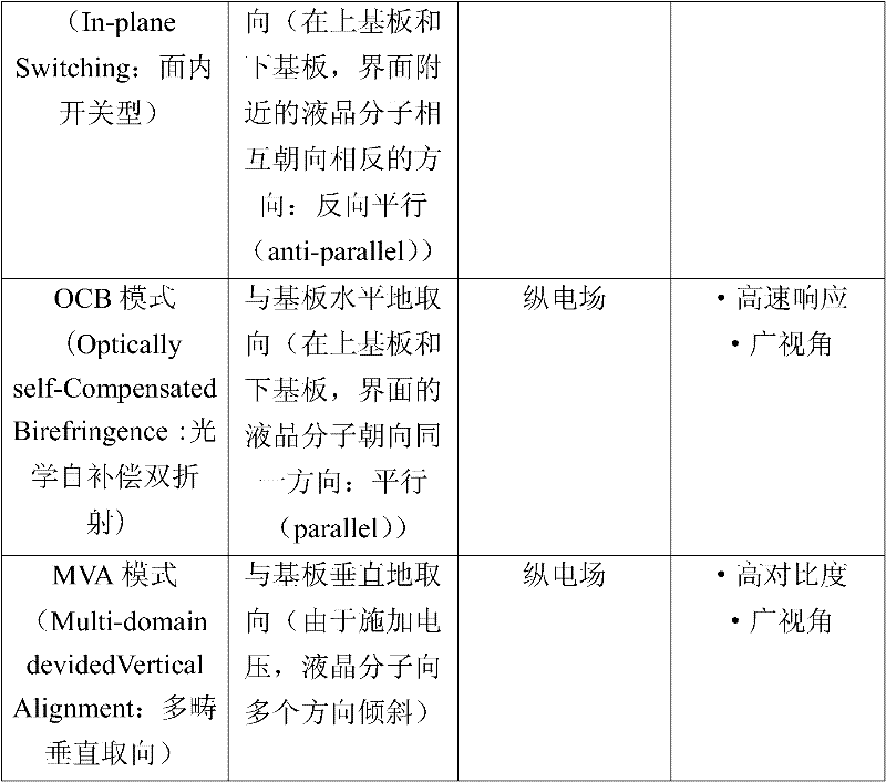
现有的LCD通过利用施加电压控制液晶分子的排列、改变透过液晶层的光的偏光状态、对通过偏光板的光量进行调节来进行显示。LCD的显示性能的很多部分由施加电压时的液晶分子的排列状态以及施加电场的大小和方向决定。LCD的显示模式大致分为垂直取向模式和水平取向模式这两种模式。表1是表示各种显示模式中显示特性根据未施加电压时的液晶分子的排列状态和施加电场的方向的不同而如何不同的。Conventional LCDs display by controlling the arrangement of liquid crystal molecules by applying voltage, changing the polarization state of light passing through the liquid crystal layer, and adjusting the amount of light passing through a polarizing plate. Much of the display performance of an LCD is determined by the alignment of liquid crystal molecules when a voltage is applied and the magnitude and direction of an applied electric field. The display modes of the LCD are roughly divided into two modes, a vertical alignment mode and a horizontal alignment mode. Table 1 shows how display characteristics differ in various display modes depending on the alignment state of liquid crystal molecules when no voltage is applied and the direction in which an electric field is applied.
[表1][Table 1]
上述各种显示模式已经被实用化,且在为了进一步提高特性而进行各种研究。例如,作为对OCB模式的研究,公开有如下方法:以迅速且可靠地以低电压进行从展曲取向状态转向弯曲取向状态的转变为目的,使用由含有固体微粒子的液晶取向剂(漆,varnish)形成的取向膜或在表面散布有固体微粒子的取向膜(例如参照专利文献1)。The various display modes described above have already been put into practical use, and various researches are being conducted to further improve the characteristics. For example, as research on the OCB mode, a method has been disclosed in which a liquid crystal aligning agent (lacquer, varnish, varnish, etc.) ) or an alignment film in which solid fine particles are dispersed on the surface (for example, refer to Patent Document 1).
此外,作为TN模式的应用,还提案有如下的横电场型TN模式:不在一对基板中的各个基板形成电极,而在一对基板中的一个基板形成一对电极产生横电场,并使其在扭曲状态和无扭曲状态之间转变(例如参照专利文献2)。In addition, as an application of the TN mode, a transverse electric field type TN mode has been proposed in which, instead of forming electrodes on each of a pair of substrates, a pair of electrodes is formed on one of a pair of substrates to generate a transverse electric field and make it Transition between a twisted state and an untwisted state (for example, refer to Patent Document 2).
进一步,还提案有GH(Guest-Host:客主)模式,其与上述各种模式不同,使用含有双色性色素的液晶层,由此,能够不需要或减少偏光板(例如参照专利文献3)。Furthermore, a GH (Guest-Host) mode is also proposed, which is different from the above-mentioned various modes, and uses a liquid crystal layer containing a dichroic dye, thereby eliminating or reducing the need for a polarizing plate (for example, refer to Patent Document 3). .
但是,满足广视角、高对比度和高速响应的所有特性的显示模式尚未被开发。However, a display mode satisfying all characteristics of wide viewing angle, high contrast ratio, and high-speed response has not yet been developed.
对此,一直以来在研究如下的显示模式:使用在同一平面上平行地相对配置的多个电极控制液晶分子的取向性,该液晶分子在未施加电压的状态下垂直取向,且具有正的介电常数各向异性(例如参照专利文献4),或如下的显示模式:在两个基板中的下部基板相互平行地形成两个电极,在未施加电场时使液晶层的液晶分子与两个基板垂直地排列,在该两个电极间形成放射线状的电场,由此,以两个电极间的区域的中心面为基准使左右的液晶分子对称取向,得到视角特性(例如参照专利文献5和6)。In view of this, a display mode has been studied in which the orientation of liquid crystal molecules that are vertically aligned in a state where no voltage is applied and have a positive dielectric strength is controlled by using a plurality of electrodes arranged oppositely in parallel on the same plane. Electrical constant anisotropy (for example, refer to Patent Document 4), or a display mode in which two electrodes are formed parallel to each other on the lower substrate of the two substrates, and the liquid crystal molecules of the liquid crystal layer are connected to the two substrates when no electric field is applied. Vertically arranged, a radial electric field is formed between the two electrodes, whereby the left and right liquid crystal molecules are aligned symmetrically with the center plane of the region between the two electrodes as a reference to obtain viewing angle characteristics (for example, refer to
现有技术文献prior art literature
专利文献patent documents
专利文献1:日本特开2002-131754号公报Patent Document 1: Japanese Patent Laid-Open No. 2002-131754
专利文献2:日本特开2002-268088号公报Patent Document 2: Japanese Patent Laid-Open No. 2002-268088
专利文献3:日本特开2001-108996号公报Patent Document 3: Japanese Patent Laid-Open No. 2001-108996
专利文献4:日本特开昭57-618号公报Patent Document 4: Japanese Patent Laid-Open No. 57-618
专利文献5:日本特开平10-333171号公报Patent Document 5: Japanese Patent Application Laid-Open No. 10-333171
专利文献6:日本特开平11-24068号公报Patent Document 6: Japanese Patent Application Laid-Open No. 11-24068
发明内容 Contents of the invention
发明所要解决的问题The problem to be solved by the invention
本发明的发明者们在对如下的显示方式进行研究:使用具有正的介电常数各向异性的(p(正)型)向列型液晶,保持基于垂直取向的高对比性,并且使用设置在同一基板的一对电极产生拱形的横电场,由此,将位于该一对电极间的液晶分子的取向方位规定为横向的弯曲状取向(以下也称为VA-IPS模式)。以下,以VA-IPS模式为例对达到本发明的经过进行说明,但是本发明并不限定于VA-IPS模式。The inventors of the present invention are researching a display method that uses a nematic liquid crystal having a positive dielectric constant anisotropy (p (positive) type), maintains high contrast based on vertical alignment, and uses a setting A pair of electrodes on the same substrate generates an arcuate transverse electric field, whereby the orientation of liquid crystal molecules located between the pair of electrodes is defined as a transverse meander alignment (hereinafter also referred to as VA-IPS mode). Hereinafter, the VA-IPS mode is taken as an example to describe the progress of the present invention, but the present invention is not limited to the VA-IPS mode.
图1是表示具有代表性的VA-IPS模式的结构的立体示意图。如图1所示,VA-IPS模式的液晶显示元件具有一对基板1、2,在该一对基板1、2间密封有液晶层3。上述一对基板1、2各自以透明基板11、12为主体,在与液晶层3侧接触的一侧的面具有垂直取向膜13、14。由此,在未对液晶层3施加电压时,液晶分子15均表现为垂直取向(垂面(homeotropic)取向)。能够通过在一对基板1、2中的一个基板形成的一对梳型电极16对液晶层3施加电压。而且,通过配置在透明基板11、12的与液晶层相反一侧的面上的偏光板17、18来选择透过或遮断光。FIG. 1 is a schematic perspective view showing the structure of a typical VA-IPS mode. As shown in FIG. 1 , a VA-IPS mode liquid crystal display element has a pair of
根据这样的基本结构,如上述专利文献5和6所示的液晶显示元件那样,通过施加电场形成弯曲状的电场,在液晶层的一对电极间区域形成指向矢方位相互对称的两个畴,因此能够得到广视角特性。Based on such a basic structure, as in the liquid crystal display elements shown in
对此,本发明的发明者们已经发现,更具体而言,通过使梳型电极的电极宽度、电极间隔和液晶层厚度最优化,能够兼得高透过率、广视角和高速响应。In this regard, the inventors of the present invention have found that, more specifically, by optimizing the electrode width, electrode interval, and liquid crystal layer thickness of the comb-shaped electrodes, high transmittance, wide viewing angle, and high-speed response can be achieved at the same time.
图2是表示施加7V的电压时的VA-IPS模式的单元内的等电位曲线的示意图。如图2所示,被施加阈值以上的电压时,液晶分子的取向受到电场强度分布和来自界面的束缚力的影响。图3是表示图2中所示的VA-IPS模式的单元内的液晶分子的取向状态的示意图。通过施加电压,液晶分子从垂直取向向横向的弯曲状取向连续地变化。这样,在VA-IPS模式的驱动中,液晶层内的液晶分子呈横向的弯曲状取向,在灰度等级响应中也能够实现高速响应。图4是表示图2中所示的VA-IPS模式的单元内的施加电压时的液晶分子的运动的示意图。随着液晶的旋转,在各畴内,以描绘相互对称的两个圆的方式发生向下的液晶的流(图4中的箭头方向),因此相互不妨碍运动,能够实现高速的响应。FIG. 2 is a schematic diagram showing equipotential curves in a cell in the VA-IPS mode when a voltage of 7 V is applied. As shown in FIG. 2 , when a voltage higher than the threshold value is applied, the orientation of the liquid crystal molecules is affected by the electric field intensity distribution and the binding force from the interface. FIG. 3 is a schematic view showing an alignment state of liquid crystal molecules in the VA-IPS mode cell shown in FIG. 2 . By applying a voltage, the liquid crystal molecules continuously change from a vertical orientation to a lateral bend orientation. In this way, during driving in the VA-IPS mode, the liquid crystal molecules in the liquid crystal layer are aligned in a laterally bent shape, and high-speed response can be realized also in the gray scale response. FIG. 4 is a schematic diagram showing movement of liquid crystal molecules when a voltage is applied in the VA-IPS mode cell shown in FIG. 2 . As the liquid crystal rotates, in each domain, a downward liquid crystal flow (arrow direction in FIG. 4 ) occurs so as to draw two symmetrical circles. Therefore, high-speed response can be realized without interfering with each other's motion.
这样,作为VA-IPS模式的特征,能够列举高速响应、广视角和高对比度,而作为透过率,表现为图5所示那样的分布。图5是表示被施加10V的电压时的VA-IPS模式的施加电压时的液晶取向分布和此时的单元内的透过率分布的示意图。如图5所示,位于一对电极的正上方的液晶分子不易受到电场的变化的影响,此外,位于离各电极最远的各电极间的中央区域的液晶分子也不易受到电场的变化的影响,因此,这些液晶分子维持垂直取向。其结果是,如图5的曲线所示,沿电极形成部和电极间中央部形成暗线,与其他显示模式相比透过率变低。In this manner, the characteristics of the VA-IPS mode include high-speed response, wide viewing angle, and high contrast, and the transmittance exhibits a distribution as shown in FIG. 5 . 5 is a schematic diagram showing the liquid crystal orientation distribution and the transmittance distribution in the cell at the time of voltage application in the VA-IPS mode when a voltage of 10 V is applied. As shown in Figure 5, the liquid crystal molecules located directly above a pair of electrodes are not easily affected by the change of the electric field. In addition, the liquid crystal molecules located in the central region between the electrodes farthest from each electrode are not easily affected by the change of the electric field. , therefore, these liquid crystal molecules maintain a vertical alignment. As a result, as shown in the graph of FIG. 5 , a dark line is formed along the electrode formation portion and the center portion between the electrodes, and the transmittance becomes lower than in other display modes.
作为提高透过率的一个方法,考虑增大液晶层中的非电极部的宽度的方法,但是,产生阈值电压上升、驱动电压上升的新问题,并且中间灰度附近的电压-透过率特性的急剧性也成为问题。图6是表示有代表性的VA-IPS模式的单元的电压-透过率特性的图表。实线是令梳型电极的电极宽度L为4μm、令电极间隔S为4μm、令液晶层厚d为4μm时的图表,虚线是令梳型电极的电极宽度L为4μm、令电极间隔S为12μm、令液晶层厚度d为4μm时的图表。另外,为了得到上述图表而使用的液晶是混合液晶MLC-6418(默克公司(メルク社)制造)。由图6可知,为了得到高透过率,需要使电极间隔S的值变大,但是驱动电压变高,因此,例如不适用于必须为低电压驱动的便携式电话,用途被限定。As one method of improving the transmittance, a method of increasing the width of the non-electrode portion in the liquid crystal layer is conceivable, but there is a new problem of an increase in the threshold voltage and an increase in the driving voltage, and the voltage-transmittance characteristics near the middle gray scale The sharpness of it also becomes a problem. FIG. 6 is a graph showing voltage-transmittance characteristics of a typical VA-IPS mode cell. The solid line is a graph when the electrode width L of the comb-shaped electrode is 4 μm, the electrode spacing S is 4 μm, and the thickness d of the liquid crystal layer is 4 μm. The dotted line is the electrode width L of the comb-shaped electrode is 4 μm, and the electrode spacing S is 12 μm, the graph when the liquid crystal layer thickness d is 4 μm. In addition, the liquid crystal used for obtaining the said graph was mixed liquid crystal MLC-6418 (made by Merck & Co., Ltd.). As can be seen from FIG. 6 , in order to obtain high transmittance, the value of the electrode spacing S needs to be increased, but the driving voltage is increased. Therefore, it is not suitable for, for example, mobile phones that must be driven at low voltage, and the application is limited.
另一方面,图7是将电极间隔S固定为4μm时将VA-IPS模式中的电压-透过率特性与其他显示模式的电压-透过率特性相比较地进行表示的图表。无论在哪个模式中,液晶材料均使用向列型液晶ZLI-4792(默克公司(メルク社)制造),并令液晶层厚d为4μm。此外,令梳型电极的电极宽度L为4μm,令电极间隔S为4μm。由图7可知,VA-IPS模式中阈值电压比其他的显示模式高,VA-IPS模式中的驱动电压的下降为其他显示模式以上这方面成为重要的问题。On the other hand, FIG. 7 is a graph showing voltage-transmittance characteristics in the VA-IPS mode compared with voltage-transmittance characteristics in other display modes when the electrode spacing S is fixed at 4 μm. In any mode, the nematic liquid crystal ZLI-4792 (manufactured by Merck) was used as the liquid crystal material, and the thickness d of the liquid crystal layer was set to 4 μm. In addition, the electrode width L of the comb-shaped electrodes was set to 4 μm, and the electrode interval S was set to 4 μm. As can be seen from FIG. 7 , the threshold voltage in the VA-IPS mode is higher than that in the other display modes, and it is an important issue that the driving voltage drop in the VA-IPS mode is higher than that in the other display modes.
本发明是鉴于上述现状而完成的,其目的在于提供一种能够以低阈值电压驱动的液晶显示元件。The present invention has been made in view of the above circumstances, and an object of the present invention is to provide a liquid crystal display element that can be driven at a low threshold voltage.
用于解决问题的方法method used to solve the problem
本发明的发明者们对令初始倾斜为垂直取向的、例如横电场方式的驱动电压的下降进行了各种研究后,着眼于VA-IPS模式的液晶分子的施加电压时的运动。而且发现,VA-IPS模式是在施加电场时液晶分子朝向非电极部的中央倒下的显示方式,在对透过率有贡献的非电极部,液晶分子从左右朝向内侧倒下,因此,形成有上述暗线的区域附近的电场的应变能变大,与在整个区域同样地发生分子旋转的其他显示模式相比,阈值电压变高。The inventors of the present invention focused on the movement of liquid crystal molecules in the VA-IPS mode when a voltage is applied after conducting various studies on the drop of the driving voltage of, for example, a transverse electric field system to make the initial tilt into a vertical alignment. In addition, it was found that the VA-IPS mode is a display method in which liquid crystal molecules fall toward the center of the non-electrode portion when an electric field is applied, and that liquid crystal molecules fall from left to right toward the inside at the non-electrode portion that contributes to the transmittance. The strain energy of the electric field near the region with the dark line becomes larger, and the threshold voltage becomes higher than in other display modes in which molecular rotation occurs uniformly in the entire region.
此外,本发明的发明者们发现,在上述液晶分子的旋转中,除了上述主要原因以外,界面束缚力、弗雷德里克兹(Freedericksz)阈值、液晶分子的配位角度、电场的强度和电场的方位也发生影响,阈值附近的透过率的急剧性由它们之间的平衡决定。In addition, the inventors of the present invention found that in the above-mentioned rotation of liquid crystal molecules, in addition to the above-mentioned factors, interfacial binding force, Fredericks (Freedericksz) threshold, coordination angle of liquid crystal molecules, intensity of electric field and electric field The orientation of is also affected, and the sharpness of the transmittance near the threshold is determined by the balance between them.
而且,本发明的发明者们进行了锐意探讨,结果发现减小在基板的与液晶层的界面的极角方向的束缚力(锚定能)的方式对阈值电压的降低有效。Furthermore, the inventors of the present invention conducted intensive studies and found that reducing the binding force (anchor energy) in the polar angle direction of the interface between the substrate and the liquid crystal layer is effective for lowering the threshold voltage.
图8是对未采用本发明的VA-IPS模式中的液晶层与基板的界面附近的液晶分子的举动进行表示的概念图。此外,图9是对本发明的VA-IPS模式中的液晶层与基板的界面附近的液晶分子的举动进行表示的概念图。如图8所示,通常在VA-IPS模式中,在电压断开(OFF)状态下,液晶分子15均呈现垂直取向,在电压导通(ON)状态下,在最接近基板11和电极16的列的液晶分子15维持垂直取向,第二接近的列的液晶分子15倾斜,而如图9所示,在本发明的构思中,设想最接近基板11和电极16的列的液晶分子15也倾斜。8 is a conceptual diagram showing the behavior of liquid crystal molecules near the interface between the liquid crystal layer and the substrate in the VA-IPS mode in which the present invention is not applied. 9 is a conceptual diagram showing the behavior of liquid crystal molecules near the interface between the liquid crystal layer and the substrate in the VA-IPS mode of the present invention. As shown in FIG. 8 , usually in the VA-IPS mode, in the voltage disconnection (OFF) state, the
进一步,本发明的发明者们对降低与液晶层的界面中的基板的极角方向的锚定能的具体方法进行了各种探讨,结果发现与液晶层构成界面的高分子膜:(i)包含具有CF2键的高分子材料;(ii)包含在侧链末端具有CF3基的高分子材料;(iii)包含具有SiO键的高分子材料;或,(iv)在表面具有深度10nm以上、100nm以下的多个凹部,由此,能够有效地减低与液晶层的界面中的基板的极角方向的锚定能,从而想到能够出色地解决上述问题,完成了本发明。Furthermore, the inventors of the present invention conducted various studies on specific methods for reducing the anchoring energy in the polar angle direction of the substrate at the interface with the liquid crystal layer, and found that the polymer film forming the interface with the liquid crystal layer: (i) Contains a polymer material with a CF bond ; (ii) contains a polymer material with a CF group at the end of the side chain; (iii) contains a polymer material with a SiO bond; or, (iv) has a depth of more than 10 nm on the surface , 100nm or less of a plurality of recesses, thereby effectively reducing the polar angle direction of the substrate in the interface with the liquid crystal layer anchoring energy, so that can solve the above problems excellently, completed the present invention.
即,本发明是包括一对基板和被密封在上述一对基板间的液晶层的液晶显示元件,上述液晶层含有在未施加电压时与上述一对基板中的至少一个基板的基板面垂直地取向的液晶分子,上述一对基板中的至少一个基板具有一对梳型电极,上述一对基板中的至少一个基板在与液晶层接触的一侧的面具有高分子膜,上述高分子膜包含具有CF2键的高分子材料(以下,也称为本发明的第一液晶显示元件)。That is, the present invention is a liquid crystal display element including a pair of substrates and a liquid crystal layer sealed between the pair of substrates, and the liquid crystal layer includes a layer perpendicular to the substrate surface of at least one of the pair of substrates when no voltage is applied. Aligned liquid crystal molecules, at least one of the above-mentioned pair of substrates has a pair of comb-shaped electrodes, at least one of the above-mentioned pair of substrates has a polymer film on the surface of the side that is in contact with the liquid crystal layer, and the above-mentioned polymer film includes A polymer material having a CF 2 bond (hereinafter also referred to as the first liquid crystal display element of the present invention).
此外,本发明是包括一对基板和被密封在上述一对基板间的液晶层的液晶显示元件,上述液晶层含有在未施加电压时与上述一对基板中的至少一个基板的基板面垂直地取向的液晶分子,上述一对基板中的至少一个基板具有一对梳型电极,上述一对基板中的至少一个基板在与液晶层接触的一侧的面具有高分子膜,上述高分子膜包含在侧链末端具有CF3基的高分子材料(以下,也称为本发明的第二液晶显示元件)。Furthermore, the present invention is a liquid crystal display element including a pair of substrates and a liquid crystal layer sealed between the pair of substrates, and the liquid crystal layer includes a layer perpendicular to the substrate surface of at least one of the pair of substrates when no voltage is applied. Aligned liquid crystal molecules, at least one of the above-mentioned pair of substrates has a pair of comb-shaped electrodes, at least one of the above-mentioned pair of substrates has a polymer film on the surface of the side that is in contact with the liquid crystal layer, and the above-mentioned polymer film includes A polymer material having a CF 3 group at a side chain terminal (hereinafter also referred to as the second liquid crystal display element of the present invention).
此外,本发明是包括一对基板和被密封在上述一对基板间的液晶层的液晶显示元件,上述液晶层含有在未施加电压时与上述一对基板中的至少一个基板的基板面垂直地取向的液晶分子,上述一对基板中的至少一个基板具有一对梳型电极,上述一对基板中的至少一个基板在与液晶层接触的一侧的面具有高分子膜,上述高分子膜包含具有SiO键的高分子材料(以下,也称为本发明的第三液晶显示元件)。Furthermore, the present invention is a liquid crystal display element including a pair of substrates and a liquid crystal layer sealed between the pair of substrates, and the liquid crystal layer includes a layer perpendicular to the substrate surface of at least one of the pair of substrates when no voltage is applied. Aligned liquid crystal molecules, at least one of the above-mentioned pair of substrates has a pair of comb-shaped electrodes, at least one of the above-mentioned pair of substrates has a polymer film on the surface of the side that is in contact with the liquid crystal layer, and the above-mentioned polymer film includes A polymer material having a SiO bond (hereinafter also referred to as the third liquid crystal display element of the present invention).
此外,本发明是包括一对基板和被密封在上述一对基板间的液晶层的液晶显示元件,上述液晶层含有在未施加电压时与上述一对基板中的至少一个基板的基板面垂直地取向的液晶分子,上述一对基板中的至少一个基板具有一对梳型电极,上述一对基板中的至少一个基板在与液晶层接触的一侧的面具有高分子膜,上述高分子膜包含无机材料,且在表面具有深度为10nm以上、100nm以下的多个凹部(以下,也称为本发明的第四液晶显示元件)。Furthermore, the present invention is a liquid crystal display element including a pair of substrates and a liquid crystal layer sealed between the pair of substrates, and the liquid crystal layer includes a layer perpendicular to the substrate surface of at least one of the pair of substrates when no voltage is applied. Aligned liquid crystal molecules, at least one of the above-mentioned pair of substrates has a pair of comb-shaped electrodes, at least one of the above-mentioned pair of substrates has a polymer film on the surface of the side that is in contact with the liquid crystal layer, and the above-mentioned polymer film includes It is an inorganic material, and has a plurality of concave portions with a depth of not less than 10 nm and not more than 100 nm on the surface (hereinafter also referred to as the fourth liquid crystal display element of the present invention).
另外,本发明与上述现有技术文献中的专利文献1~3在以下方面不同。In addition, the present invention differs from
在上述专利文献1,在OCB模式中,使固体微粒子散布在取向膜表面,通过将该固体微粒子作为从展曲取向状态转向弯曲取向状态的转变的核,实现用于上述转变的初始化电压的降低。即,认为在取向膜表面的存在微粒子的部分,微小区域的取向紊乱,局部形成扭曲取向,弯曲转变变得容易,与减弱锚定能降低转变电压的构思不同。In the above-mentioned
在上述专利文献2中,组合横电场施加方式和a-TN模式,使具有一对电极的透明基板一侧的与液晶层的界面的锚定强度比不具有一对电极的透明基板侧的与液晶层的界面的锚定强度大,由此维持扭曲取向不变地利用电场使TN液晶旋转,能够以比通常的TN模式低的电压进行开关。但是,此处的锚定强度表示方位角方向的锚定(anchoring),对极角方向的锚定没有任何涉及。此外,在该方式中,存在不易控制各畴的边界区域,不能实现高对比度的显示的问题。In the
在上述专利文献3中,在GH模式中,通过使用化学吸附膜调整锚定使液晶分子容易运动,实现高速响应。虽然公开有利用在长链末端具有碳化氟基的化学吸附膜的垂直取向膜,但是并未说明由此实现的低电压化的效果。一般化学吸附膜为超薄膜,由于膜引起的电压损失少而实现低电压化。In the above-mentioned
以下,对本发明的第一~第四液晶显示元件进行详细说明。Hereinafter, the first to fourth liquid crystal display elements of the present invention will be described in detail.
本发明的第一~第四液晶显示元件是包括一对基板和被密封在上述一对基板间的液晶层的液晶显示元件。在上述液晶层,填充有通过施加一定的电压控制取向性的液晶分子。通过在上述一对基板的一方或双方设置配线、电极、半导体元件等,能够对液晶层内施加电压,控制液晶分子的取向性。The first to fourth liquid crystal display elements of the present invention are liquid crystal display elements including a pair of substrates and a liquid crystal layer sealed between the pair of substrates. The liquid crystal layer is filled with liquid crystal molecules whose orientation is controlled by applying a constant voltage. By providing wiring, electrodes, semiconductor elements, etc. on one or both of the pair of substrates, a voltage can be applied to the liquid crystal layer to control the orientation of the liquid crystal molecules.
上述液晶层含有在未施加电压时与上述一对基板中的至少一个基板的基板面垂直地取向的液晶分子。通过令液晶分子的初始取向为垂直取向,能够有效地进行黑显示时的光的遮断。The liquid crystal layer includes liquid crystal molecules aligned perpendicular to a substrate surface of at least one of the pair of substrates when no voltage is applied. By setting the initial orientation of the liquid crystal molecules to be a vertical orientation, it is possible to efficiently block light during black display.
上述一对基板中的至少一个基板具有一对梳型电极。上述梳型电极只要具有成为梳柄的部分和从柄平面地突出的梳齿,其整体结构就不被特别限定。上述一对梳型电极中,例如使一个梳型电极为按图像元素单位设置且被施加信号电压的图像元素电极,使另一个梳型电极为被施加维持在一定电压的共用电压的共用电极,由此,能够根据被供给至图像元素电极的图像信号,按每个图像元素形成电场(例如横向的电场)。At least one of the pair of substrates has a pair of comb electrodes. The overall structure of the above-mentioned comb electrode is not particularly limited as long as it has a portion serving as a handle and comb teeth protruding planarly from the handle. Among the above-mentioned pair of comb-shaped electrodes, for example, one comb-shaped electrode is a picture element electrode provided in units of picture elements and a signal voltage is applied, and the other comb-shaped electrode is a common electrode to which a common voltage maintained at a certain voltage is applied, Accordingly, an electric field (for example, a horizontal electric field) can be formed for each picture element based on an image signal supplied to the picture element electrode.
上述一对基板中的至少一个基板在与液晶层接触一侧的面具有高分子膜。上述高分子膜优选为将接近表面的液晶分子的倾斜规定为与极角方向成大致90°(90°±0~4°)的垂直取向膜,该初始取向既可以起因于高分子膜的材料,也可以起因于高分子膜的构造。At least one of the pair of substrates has a polymer film on a surface that is in contact with the liquid crystal layer. The above-mentioned polymer film is preferably a vertical alignment film in which the inclination of the liquid crystal molecules close to the surface is defined to be approximately 90° (90° ± 0 to 4°) from the polar angle direction, and this initial alignment may be caused by the material of the polymer film , can also be caused by the structure of the polymer film.
在本发明的第一液晶显示元件中,上述高分子膜包含具有CF2键的高分子材料,在本发明的第二液晶显示元件中,上述高分子膜包含在侧链末端具有CF3基的高分子材料。优选上述高分子材料具有CF2键且在侧链末端具有CF3基。此外,优选具有上述CF2键的高分子材料和/或在上述侧链末端具有CF3基的高分子材料的每个重复单元的F原子的比例为5重量%以上。上述高分子材料含有F(氟)原子,由此,上述高分子膜的表面能量下降,因此,对液晶分子的锚定能也下降。此外,因为F原子能够减小对离子性杂质的亲和性,所以能够抑制在高分子膜的表面形成双电层(electric double layer)的情况。In the first liquid crystal display element of the present invention, the above-mentioned polymer film comprises a polymer material having a CF bond , and in the second liquid crystal display element of the present invention, the above-mentioned polymer film comprises a polymer material having a CF group at a side chain end. Polymer Materials. The above-mentioned polymer material preferably has a CF 2 bond and a CF 3 group at the end of the side chain. In addition, it is preferable that the ratio of F atoms per repeating unit of the polymer material having the aforementioned CF 2 bond and/or the polymer material having the CF 3 group at the end of the side chain is 5% by weight or more. The above-mentioned polymer material contains F (fluorine) atoms, whereby the surface energy of the above-mentioned polymer film is lowered, and therefore, the anchoring energy to liquid crystal molecules is also lowered. In addition, since the F atoms can reduce the affinity for ionic impurities, it is possible to suppress the formation of an electric double layer on the surface of the polymer film.
在本发明的第三液晶显示元件,上述高分子膜包含具有SiO键的高分子材料。对具有SiO键的高分子膜表面的液晶分子的锚定能比对不具有SiO键的高分子膜表面的液晶分子的锚定能小一位以上。因此,通过使用具有SiO键的高分子材料能够减小对液晶分子的锚定能。In the third liquid crystal display element of the present invention, the polymer film includes a polymer material having SiO bonds. The anchoring energy to liquid crystal molecules on the surface of the polymer film having SiO bonds is lower than the anchoring energy to liquid crystal molecules on the surface of the polymer film not having SiO bonds by one bit or more. Therefore, anchoring energy to liquid crystal molecules can be reduced by using a polymer material having SiO bonds.
此外,由于Si(硅)原子的比例越大就越有助于阈值电压的下降,因此,上述高分子材料的每个重复单元的Si(硅)原子的比例优选为5重量%以上,考虑到高分子膜的成膜性和对液晶分子的取向限制性,优选上述高分子材料的每个重复单元的Si原子的比例为30重量%以下。In addition, since the larger ratio of Si (silicon) atoms contributes to the reduction of the threshold voltage, the ratio of Si (silicon) atoms per repeating unit of the above-mentioned polymer material is preferably 5% by weight or more. In terms of the film-forming property of the polymer film and the orientation restriction of liquid crystal molecules, it is preferable that the proportion of Si atoms per repeating unit of the polymer material is 30% by weight or less.
在本发明的第四液晶显示元件,上述高分子膜包含无机材料,在表面具有深度为10nm以上、100nm以下的多个凹部。此处的高分子膜不是一般作为取向膜使用的聚酰亚胺等有机膜而是无机膜,在表面具有满足上述数值范围的微细的凹凸形状。采用这样的无机膜,与使用有机膜的情况相比,能够将锚定能减小一位以上。此外,虽然在均匀性方面不如上述聚酰亚胺膜,但是能够使液晶分子垂直取向。In the fourth liquid crystal display element of the present invention, the polymer film includes an inorganic material, and has a plurality of concave portions having a depth of not less than 10 nm and not more than 100 nm on the surface. The polymer film here is not an organic film such as polyimide generally used as an alignment film, but an inorganic film, and has a fine uneven shape satisfying the above numerical range on the surface. With such an inorganic film, the anchoring energy can be reduced by one bit or more compared to the case of using an organic film. In addition, although inferior in uniformity to the above-mentioned polyimide film, liquid crystal molecules can be vertically aligned.
在本发明的第一~第四液晶显示元件,优选上述液晶分子为具有正的介电常数各向异性的向列型液晶分子。由此,通过向液晶层施加电压,液晶分子沿着电场的朝向取向,能够得到广视角。另外,通过向液晶层施加电压,液晶分子组例如描绘出拱形。In the first to fourth liquid crystal display elements of the present invention, it is preferable that the liquid crystal molecules are nematic liquid crystal molecules having positive dielectric constant anisotropy. Accordingly, by applying a voltage to the liquid crystal layer, the liquid crystal molecules are aligned along the direction of the electric field, and a wide viewing angle can be obtained. In addition, by applying a voltage to the liquid crystal layer, the group of liquid crystal molecules draws, for example, a domed shape.
作为本发明的液晶显示元件的结构,只要将这样的构成要素作为必须的构成要素而形成,就不特别地被其他的构成要素限定。The structure of the liquid crystal display element of the present invention is not particularly limited to other constituent elements as long as it is formed with such constituent elements as essential constituent elements.
发明的效果The effect of the invention
根据本发明,令初始倾斜为垂直取向的液晶显示元件(例如横电场方式的液晶显示元件)也能够进行低电压驱动。According to the present invention, it is also possible to drive a liquid crystal display element whose initial inclination is a vertical alignment (for example, a liquid crystal display element of a transverse electric field system) at a low voltage.
附图说明 Description of drawings
图1是表示本发明和有代表性的VA-IPS模式的结构的立体示意图。FIG. 1 is a schematic perspective view showing the structure of the present invention and a typical VA-IPS mode.
图2是表示被施加7V的电压时本发明和有代表性的VA-IPS模式的单元内的等电位曲线的示意图。FIG. 2 is a schematic diagram showing equipotential curves in the cells of the present invention and a typical VA-IPS mode when a voltage of 7 V is applied.
图3是表示图2所示的VA-IPS模式的单元内的液晶分子的取向状态的示意图。FIG. 3 is a schematic diagram showing an alignment state of liquid crystal molecules in the VA-IPS mode cell shown in FIG. 2 .
图4是表示图2所示的VA-IPS模式的单元内的施加电压时的液晶分子的运动的示意图。FIG. 4 is a schematic diagram showing movement of liquid crystal molecules when a voltage is applied in the VA-IPS mode cell shown in FIG. 2 .
图5是表示被施加10V的电压时本发明和有代表性的VA-IPS模式的施加电压时的液晶取向分布和此时的单元内的透过率分布的示意图。5 is a schematic diagram showing the liquid crystal orientation distribution and the transmittance distribution in the cell at the time of voltage application in the present invention and a typical VA-IPS mode when a voltage of 10 V is applied.
图6是表示本发明以及有代表性的VA-IPS模式的单元的电压-透过率特性的图表。FIG. 6 is a graph showing voltage-transmittance characteristics of the present invention and a typical VA-IPS mode cell.
图7是在将电极间隔S固定为4μm时,将VA-IPS模式的电压-透过率特性与其他显示模式的电压-透过率特性比较地进行表示的图表。FIG. 7 is a graph showing voltage-transmittance characteristics of the VA-IPS mode in comparison with voltage-transmittance characteristics of other display modes when the electrode spacing S is fixed at 4 μm.
图8是对未采用本发明的VA-IPS模式的液晶层与基板的界面附近的液晶分子的举动进行表示的概念图。8 is a conceptual diagram showing the behavior of liquid crystal molecules in the vicinity of the interface between the liquid crystal layer and the substrate in the VA-IPS mode of the present invention.
图9是对采用本发明的VA-IPS模式的液晶层与基板的界面附近的液晶分子的举动进行表示的概念图。9 is a conceptual diagram showing the behavior of liquid crystal molecules near the interface between the liquid crystal layer and the substrate in the VA-IPS mode of the present invention.
图10是表示实施方式1的液晶显示元件的电场的方位与偏光板的透过轴的关系的示意图。10 is a schematic diagram showing the relationship between the orientation of the electric field and the transmission axis of the polarizing plate in the liquid crystal display element according to the first embodiment.
图11是实施方式1的液晶显示元件的截面示意图。FIG. 11 is a schematic cross-sectional view of a liquid crystal display element in
图12是表示实施例1和比较例1的液晶显示元件的室温下的电压-透过率特性的图表。12 is a graph showing the voltage-transmittance characteristics at room temperature of the liquid crystal display elements of Example 1 and Comparative Example 1. FIG.
图13是表示实施方式8的液晶显示元件的结构的截面示意图。13 is a schematic cross-sectional view showing the structure of a liquid crystal display element in
图14是表示实施方式8的液晶显示元件的结构的平面示意图。14 is a schematic plan view showing the structure of a liquid crystal display element in
具体实施方式 Detailed ways
以下列举实施方式,参照附图对本发明进行更详细的说明,本发明并不仅限于这些实施方式。Embodiments are listed below, and the present invention will be described in more detail with reference to the drawings, but the present invention is not limited to these embodiments.
实施方式1
实施方式1的液晶显示元件是对含有在未施加电压状态下与基板面垂直地取向的p型向列型液晶(具有正的介电常数各向异性的向列型液晶)的液晶层施加横方向(基板面方向)的电场,使液晶层中的液晶分子转变为横方向的弯曲状取向的VA-IPS模式的液晶显示元件。In the liquid crystal display element of
实施方式1的液晶显示元件通过进一步包括背光源(照明装置)等,能够作为便携式电话、PDA、汽车导航仪、计算机监视器、电视机、车站内的引导板、室外告示栏等信息显示装置等使用。The liquid crystal display device according to
图1还是表示实施方式1的液晶显示元件的立体示意图。如图1所示,实施方式1的液晶显示元件包括以透明基板11为主体的阵列基板1和以透明基板11为主体的对置基板2这一对基板,在TFT基板1与对置基板2之间密封有含有p型向列型液晶分子15的液晶层3。液晶层3中的液晶分子15向与基板1、2各自的主面垂直的方向取向(垂面取向)。FIG. 1 is also a schematic perspective view showing the liquid crystal display element of the first embodiment. As shown in FIG. 1 , the liquid crystal display element of
阵列基板1具有用于向液晶层3内施加一定电压的一对梳型电极16。此外,在阵列基板1和对置基板2的与液晶层3接触的面配置有高分子膜(取向膜)14。The
在实施方式1,高分子膜14例如能够使用包含含有下述化学式(1)所示的化学构造的高分子材料的聚酰亚胺制垂直取向膜。下述化学式(1)在作为主链的二胺化合物的侧链末端具有CF3基。In
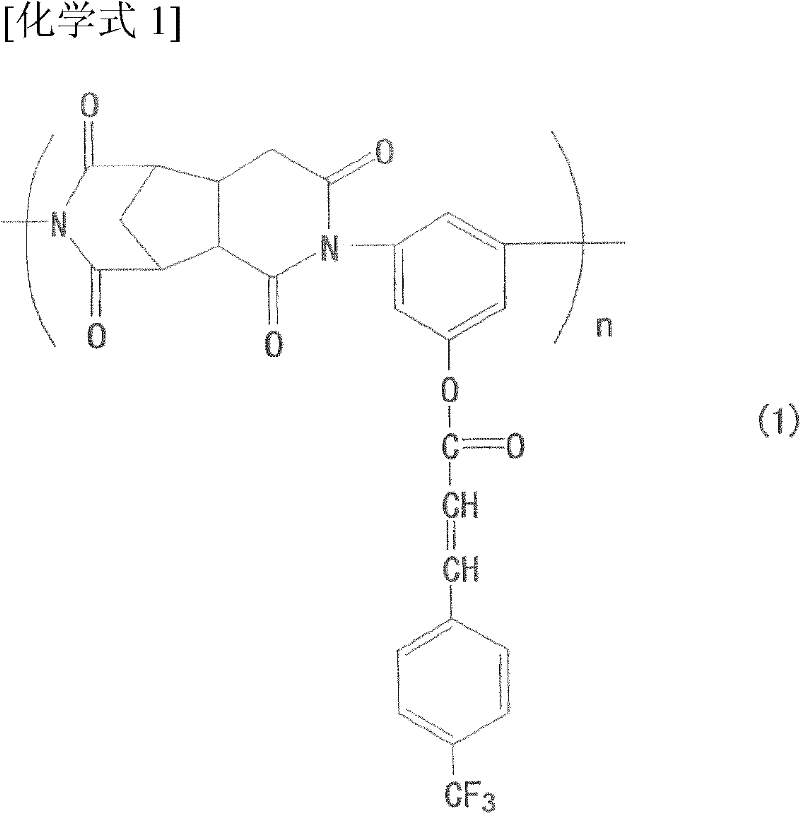
(式中,n表示括弧内的重复构造的数目,是正整数。)(In the formula, n represents the number of repeated structures in parentheses, which is a positive integer.)
作为实施方式1的高分子膜14的材料,在化学构造中的侧链末端具有CF3基即可,在聚酰亚胺树脂以外,例如还能够使用丙烯树脂、聚苯乙烯树脂、聚酯树脂、聚丙烯树脂。As the material of the
一对梳型电极分别是图像元素电极和共用电极,作为基本结构包括梳齿。图像元素电极的梳齿与共用电极的梳齿相互平行,隔开间隔互相交替地咬合。图像元素电极是按构成显示区域的每个图像元素单位配置的电极,被供给图像信号。另一方面,共用电极是与图像元素的边界无关的整体导通的电极,被供给共用信号。A pair of comb-shaped electrodes are respectively a picture element electrode and a common electrode, and include comb teeth as a basic structure. The comb teeth of the picture element electrodes and the comb teeth of the common electrode are parallel to each other, and alternately engage with each other at intervals. The picture element electrode is an electrode arranged for each picture element unit constituting the display area, and is supplied with an image signal. On the other hand, the common electrode is an electrode that is conducted as a whole regardless of the boundaries of picture elements, and is supplied with a common signal.
当对一对梳型电极施加规定电压时,在液晶层内产生拱形的电场。而且,p型向列型液晶分子沿着施加电场在横向弯曲状取向。此外,在电极形成部和电极间中央部,维持垂直取向,位于非电极部的液晶分子有助于透过。因此,实施方式1的液晶显示元件所具有的液晶层内的电场的朝向、液晶分子的取向、透过率分布等表现出与图2~5所示相同的趋势。When a predetermined voltage is applied to the pair of comb-shaped electrodes, an arc-shaped electric field is generated in the liquid crystal layer. Furthermore, the p-type nematic liquid crystal molecules are aligned in a bend-like direction along the applied electric field. In addition, the vertical alignment is maintained in the electrode formation portion and the central portion between the electrodes, and the liquid crystal molecules located in the non-electrode portion contribute to transmission. Therefore, the orientation of the electric field in the liquid crystal layer, the orientation of the liquid crystal molecules, the transmittance distribution, and the like in the liquid crystal display element of
在各透明基板11、12的与液晶层3相反一侧的面上分别配置有偏光板17、18。图10是使实施方式1的液晶显示元件的电场的方位与偏光板的透过轴的关系的示意图。虚线箭头是阵列基板一侧的偏光板的透过轴51,实线箭头是对置基板一侧的偏光板的透过轴52。此外,白色中空箭头表示电场的施加方位53。如图10所示,阵列基板一侧的偏光板的透过轴51与对置基板一侧的偏光板的透过轴52为相互成大致90°的角度的正交尼克尔的关系。此外,这些透过轴分别以相对于电场的方向即与一对梳型电极16的各梳齿的长度方向正交的方向(电场的施加方向)成大致45°的角度的方式被调节。由此,在未施加电压状态下,光状态不变地直接透过液晶层并被偏光板遮断,另一方面,在施加阈值以上的电压状态下,光受到液晶层的影响而发生双折射,透过偏光板。Polarizers 17 and 18 are disposed on the surfaces of the
图11是实施方式1的液晶显示元件的截面示意图。实施方式1的液晶显示元件在阵列基板1与对置基板2之间具有规定液晶层3的厚度(单元间隙)的珠状间隔物21和用于密封液晶层3的密封部件22。FIG. 11 is a schematic cross-sectional view of a liquid crystal display element in
以下,对实际制作实施方式1的液晶显示元件并与现有的液晶显示元件对比地进行评价的结果进行说明。具体而言,如以下所述制作实施方式1的液晶显示元件。Hereinafter, the result of actually manufacturing the liquid crystal display element of
首先,准备阵列基板一侧的玻璃基板,该基板在表面上具备ITO(Indium Tin Oxide:氧化铟锡)制的一对梳型电极,在该玻璃基板上和一对梳型电极上,利用旋涂法涂布具有上述化学式(1)所示的化学构造的垂直取向膜用聚酰亚胺溶液(5重量%、NMP溶液),然后,将涂布该溶液后的基板在200℃烧制1小时,形成了高分子膜。烧制后的高分子膜的膜厚为600
接着,利用相同的工序,在对置基板一侧的玻璃基板上也形成高分子膜。然后,在阵列基板上散布4微米树脂珠(商品名称:ミクロパ一ル(Micropearl)SP,积水化学工业株式会社制造),另一方面,在对置基板上印刷密封树脂(商品名称氨基甲酸乙脂乳胶(Structbond,ストラクトボンド)XN-21-S,三井东压化学工业株式会社制造),将它们贴合,进一步,以250℃烧制3小时,由此制作了液晶单元。另外,令单元间隙为4μm。Next, by the same process, a polymer film was also formed on the glass substrate on the counter substrate side. Then, 4 micron resin beads (trade name: Micropearl (Micropearl) SP, manufactured by Sekisui Chemical Co., Ltd.) were scattered on the array substrate, and on the other hand, sealing resin (trade name urethane) was printed on the counter substrate. Fat latex (Structbond, Straktobond) XN-21-S, manufactured by Mitsui Topress Chemical Co., Ltd.), these were bonded together, and further, fired at 250° C. for 3 hours, thereby producing a liquid crystal cell. In addition, the cell gap was set to be 4 μm.
然后,利用真空注入法将液晶组成物(默克公司制造)封入液晶单元内,接着,在各玻璃基板的、与液晶层相反一侧的面上贴合偏光板,制作了液晶显示元件(实施例1)。另外,电场施加的方位与偏光板的轴方位的关系如图10所示。封入到上述一对基板间的液晶组成物(默克公司制造)的Δn为0.112,Δε为18.5。Then, a liquid crystal composition (manufactured by Merck) was sealed in a liquid crystal cell by a vacuum injection method, and then a polarizing plate was bonded to the surface of each glass substrate opposite to the liquid crystal layer to fabricate a liquid crystal display element (Example example 1). In addition, the relationship between the orientation of the electric field application and the axial orientation of the polarizing plate is as shown in FIG. 10 . Δn of the liquid crystal composition (manufactured by Merck) sealed between the pair of substrates was 0.112, and Δε was 18.5.
然后,最后使用大冢电子株式会社制造的液晶评价装置LCD-5200测定了实施例1的液晶显示元件的电压-透过率特性。And finally, the voltage-transmittance characteristic of the liquid crystal display element of Example 1 was measured using the LCD-5200 liquid crystal evaluation apparatus by Otsuka Electronics Co., Ltd. manufacture.
此外,除了高分子膜的材料使用具有以下述化学式(2)表示的化学构造的垂直取向膜用聚酰亚胺溶液(5重量%,NMP溶液)以外,利用与实施例1时相同的方法制作比较用的液晶显示元件(比较例1)并同样测定了电压-透过率特性。In addition, a polyimide solution (5% by weight, NMP solution) for vertical alignment films (5% by weight, NMP solution) having a chemical structure represented by the following chemical formula (2) was used as the material of the polymer film, and was produced by the same method as in Example 1. The voltage-transmittance characteristics of the comparative liquid crystal display element (Comparative Example 1) were measured in the same manner.
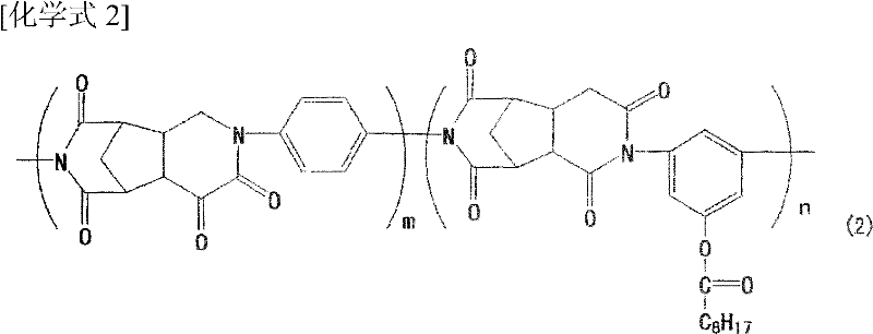
(式中,m和n表示括弧内的重复构造的数目,是正整数。此外,n=4m)(In the formula, m and n represent the number of repeated structures in parentheses, which are positive integers. In addition, n=4m)
图12是表示实施例1和比较例1的液晶显示元件的室温下的电压-透过率特性的图表。以下,作为用于看到阈值电压降低效果的指标,将为了在令液晶显示元件的最大透过率为100%时得到10%的透过率所需的电压定义为阈值电压“V10”。实施例1的液晶显示元件的V10为2.13V,比较例1的液晶显示元件的V10为2.66V。12 is a graph showing the voltage-transmittance characteristics at room temperature of the liquid crystal display elements of Example 1 and Comparative Example 1. FIG. Hereinafter, as an index for seeing the effect of lowering the threshold voltage, the voltage required to obtain a transmittance of 10% when the maximum transmittance of the liquid crystal display element is 100% is defined as the threshold voltage "V10". The V10 of the liquid crystal display element of Example 1 was 2.13V, and the V10 of the liquid crystal display element of Comparative Example 1 was 2.66V.
如图12所示,可知在实施例1的液晶显示元件能够不牺牲透过率特性而使阈值电压V10下降0.5V以上,实用上的价值大。As shown in FIG. 12 , it can be seen that the liquid crystal display element of Example 1 can reduce the threshold voltage V10 by 0.5 V or more without sacrificing the transmittance characteristics, which is of great practical value.
接着,为了调查构成实施方式1的液晶显示元件所具备的高分子膜的高分子材料中的F原子的比例的影响,使用与实施例1时相同的方法,制作了成为评价对象的液晶显示元件。具体而言,制作了使高分子材料中的上述化学式(1)的比例与上述化学式(2)的比例分别不同的液晶显示元件(实施例2~5,比较例1)。下述表2是将各实施例和比较例的结果整理而成的表。Next, in order to investigate the influence of the ratio of F atoms in the polymer material constituting the polymer film included in the liquid crystal display element of
[表2][Table 2]
如表2所示,可知阈值电压的值随着F原子的比例增加而降低,特别是在高分子材料的每个重复单元的F原子的比例为5重量%以上时(实施例1~3),显著地获得阈值电压降低的效果。As shown in Table 2, it can be seen that the value of the threshold voltage decreases as the proportion of F atoms increases, especially when the proportion of F atoms per repeating unit of the polymer material is 5% by weight or more (Examples 1-3) , the effect of lowering the threshold voltage is remarkably obtained.
另外,F原子的重量比例基于“含有F原子的高分子的混合比例”ד含有F原子的高分子的重复单元中的F原子的比例”计算出。此外,在上述F原子的比例的分析中,使用傅立叶变换红外分光法(FT-IR:Fourier Transform Infrared Spectroscopy)和X射线光电子能谱法(XPS:X-ray Photoelectron Spectroscopy)。In addition, the weight ratio of F atoms is calculated based on "the mixing ratio of the F atom-containing polymer" x "the ratio of F atoms in the repeating unit of the F atom-containing polymer". In addition, in the analysis of the ratio of the above-mentioned F atoms, Fourier transform infrared spectroscopy (FT-IR: Fourier Transform Infrared Spectroscopy) and X-ray photoelectron spectroscopy (XPS: X-ray Photoelectron Spectroscopy) were used.
实施方式2
实施方式2的液晶显示元件除了设置在与液晶层的界面的高分子膜的结构不同以外,具有与实施方式1的液晶显示元件相同的结构。在实施方式2,高分子膜(取向膜)包含在侧链具有CF2键,且在侧链末端具有CF3基的高分子材料。The liquid crystal display element of
具体而言,如下所述地,制作了实施方式2的液晶显示元件。Specifically, the liquid crystal display element of
首先,准备阵列基板一侧的玻璃基板,该基板在表面上具备ITO制的一对梳型电极,将该玻璃基板和一对梳型电极浸在下述化学式(3)所示的硅烷偶联剂的0.01mol/l三氯甲烷-NMP混合溶液(三氯甲烷∶NMP=1∶10)5分钟,接着,在干燥氮中以120℃的条件使其干燥1小时,形成了高分子膜。另外,令具有一对梳型电极的梳齿的宽度为4μm,令梳齿彼此之间的间隔为4μm。First, prepare a glass substrate on the side of the array substrate, the substrate is provided with a pair of comb-shaped electrodes made of ITO on the surface, and the glass substrate and a pair of comb-shaped electrodes are immersed in a silane coupling agent represented by the following chemical formula (3). 0.01 mol/l chloroform-NMP mixed solution (chloroform:NMP=1:10) for 5 minutes, followed by drying in dry nitrogen at 120°C for 1 hour to form a polymer film. In addition, the width of the comb teeth having a pair of comb-shaped electrodes was set to 4 μm, and the interval between the comb teeth was set to 4 μm.
[化学式3][chemical formula 3]
CF3-(CF2)17-SiCl3 (3)CF 3 -(CF 2 ) 17 -SiCl 3 (3)
接着,利用相同的工序,在对置基板一侧的玻璃基板上也形成同样的高分子膜。然后,在阵列基板上散布4微米树脂珠(商品名称:ミクロパ一ル(Micropearl)SP,积水化学工业株式会社制造),另一方面,在对置基板上印刷密封树脂(商品名称:氨基甲酸乙脂乳胶(Structbond,ストラクトボンド)XN-21-S,三井东压化学工业株式会社制造),将它们贴合,以250℃烧制3小时,由此制作了液晶单元。另外,令单元间隙为4μm。Next, the same polymer film was also formed on the glass substrate on the counter substrate side by the same process. Then, 4 micron resin beads (trade name: Micropearl (Micropearl) SP, manufactured by Sekisui Chemical Industry Co., Ltd.) were scattered on the array substrate, and on the other hand, sealing resin (trade name: urethane) was printed on the counter substrate. Ethyl emulsion (Structbond, Structbond) XN-21-S, manufactured by Mitsui Toatsu Chemical Co., Ltd.) was bonded together and fired at 250° C. for 3 hours to fabricate a liquid crystal cell. In addition, the cell gap was set to be 4 μm.
然后,利用真空注入法将液晶组成物(默克公司制造)封入液晶单元内,接着,在各玻璃基板的与液晶层相反一侧的面上贴合偏光板,制作了液晶显示元件(实施例6)。另外,电场施加的方位与偏光板的轴方位的关系如图10所示。封入在上述一对基板间的液晶组成物(默克公司制造)的Δn为0.112,Δε为18.5。Then, a liquid crystal composition (manufactured by Merck) was sealed in a liquid crystal cell by a vacuum injection method, and then a polarizing plate was attached to the surface of each glass substrate opposite to the liquid crystal layer to produce a liquid crystal display element (Example 6). In addition, the relationship between the orientation of the electric field application and the axial orientation of the polarizing plate is as shown in FIG. 10 . Δn of the liquid crystal composition (manufactured by Merck) sealed between the pair of substrates was 0.112, and Δε was 18.5.
最后,利用与实施例1时相同的方法测定了液晶显示元件的电压-透过率特性。其结果是,实施例6的液晶显示元件的V10为2.06V,实现了大幅的驱动电压的降低。另外,构成实施例6的液晶显示元件所具备的高分子膜的高分子材料的每个重复单元的F原子的比例为52.5重量%。Finally, the voltage-transmittance characteristics of the liquid crystal display element were measured by the same method as in Example 1. As a result, V10 of the liquid crystal display element of Example 6 was 2.06 V, and a significant reduction in driving voltage was achieved. In addition, the ratio of F atoms per repeating unit of the polymer material constituting the polymer film included in the liquid crystal display element of Example 6 was 52.5% by weight.
这样制作的实施例6的液晶显示元件所具备的高分子膜是单分子吸附膜,如在上述工序中说明的那样,由于仅浸在溶液中就能够得到均匀的高分子膜,因此与实施例1~5的液晶显示元件的情况相比可以说能够通过更简便的成膜工艺制作。The polymer film included in the liquid crystal display element of Example 6 produced in this way is a monomolecular adsorption film. As described in the above-mentioned process, since a uniform polymer film can be obtained only by immersing in a solution, it is similar to that of Example 6. It can be said that the liquid crystal display elements of 1 to 5 can be produced by a simpler film-forming process than in the case of the liquid crystal display elements.
在VA-IPS模式以外的主要的显示方式中,需要对高分子膜赋予一定以上的预倾(初始倾斜)角特性,不容易以单分子吸附膜控制液晶分子的预倾角,但是在VA-IPS模式的显示方式中,不需要进行液晶分子的精密的预倾角控制。因此,上述那样的形成单分子吸附膜的方法非常适合于VA-IPS模式的显示方式。此外,单分子吸附膜是分子等级的超薄膜,取向膜的电压损失也少,因此从这方面也可以说适合于VA-IPS模式的显示方式。In the main display modes other than VA-IPS mode, it is necessary to give the polymer film more than a certain pretilt (initial tilt) angle characteristic, and it is not easy to control the pretilt angle of liquid crystal molecules with a monomolecular adsorption film, but in VA-IPS In the mode display method, precise pretilt angle control of liquid crystal molecules is not required. Therefore, the method of forming a monomolecular adsorption film as described above is very suitable for the display method of the VA-IPS mode. In addition, the monomolecular adsorption film is a molecular-level ultra-thin film, and the voltage loss of the alignment film is also small, so it can also be said that it is suitable for the display method of the VA-IPS mode in this respect.
实施方式3
实施方式3的液晶显示元件在设置在与液晶层的界面的高分子膜的结构不同以外,具有与实施方式1的液晶显示元件相同的结构。在实施方式3,高分子膜(取向膜)包含具有CF2键的高分子材料。The liquid crystal display element of
具体而言,如下所述地制作了实施方式3的液晶显示元件。Specifically, the liquid crystal display element of
首先,准备阵列基板一侧的玻璃基板,该基板在表面上具备ITO制的一对梳型电极,接着,对将锚定能强的聚酰亚胺材料和锚定能弱的氟化材料以规定的比例混合而成的聚酰亚胺材料进行制作,利用LB(Langmuir-Blodgett)法在该玻璃基板上和一对梳型电极上形成高分子膜(LB膜)。First, prepare a glass substrate on the side of the array substrate, which has a pair of comb-shaped electrodes made of ITO on the surface. A polyimide material mixed in a predetermined ratio was produced, and a polymer film (LB film) was formed on the glass substrate and a pair of comb-shaped electrodes by the LB (Langmuir-Blodgett) method.
以下详细说明上述聚酰亚胺材料的制作方法。首先,将下述化学式(4)所示的四羧酸二酐5mmol和下述化学式(5)所示的二胺(diamine)5mmol在脱水后的N,N-二甲基乙酰胺20ml中以25℃搅拌3小时,使其缩聚,由此得到下述化学式(6)所示的聚酰胺酸。The manufacturing method of the above-mentioned polyimide material will be described in detail below. First, 5 mmol of tetracarboxylic dianhydride shown in the following chemical formula (4) and 5 mmol of diamine (diamine) shown in the following chemical formula (5) were added to 20 ml of N,N-dimethylacetamide after dehydration. The polyamic acid represented by the following chemical formula (6) was obtained by stirring and polycondensing at 25 degreeC for 3 hours.
接着,使下述化学式(6)所示的聚酰胺酸和下述化学式(7)所示的N,N-二甲基正十六胺(dimethyl hexadecylamine)在N,N-二甲基乙酰胺与苯的混合溶液(体积比1∶1)中反应,形成下述化学式(8)所示的聚酰胺酸的烷基胺盐,使其在基板上累积。累积条件为表面压15mN/m、上升速度15mm/min、累积温度20℃。Then, make polyamic acid shown in following chemical formula (6) and N,N-dimethyl n-hexadecylamine (dimethyl hexadecylamine) shown in following chemical formula (7) in N,N-dimethylacetamide React with benzene in a mixed solution (volume ratio 1:1) to form an alkylamine salt of polyamic acid represented by the following chemical formula (8), and accumulate it on the substrate. The accumulation conditions were a surface pressure of 15 mN/m, a rising speed of 15 mm/min, and an accumulation temperature of 20°C.
然后,将利用上述方法制作的累积膜按每个基板浸在无水醋酸、氮苯和苯的混合溶液(体积比1∶1∶3)中12小时,得到以下述化学式(9)所示的聚酰亚胺(以下简称为PI。)为材料的累积膜(取向膜)。Then, the cumulative film made by the above method was immersed in the mixed solution (volume ratio 1:1:3) of anhydrous acetic acid, nitrogen benzene and benzene for 12 hours according to each substrate, to obtain the compound shown in the following chemical formula (9): Polyimide (hereinafter abbreviated as PI.) is an accumulation film (orientation film) of the material.
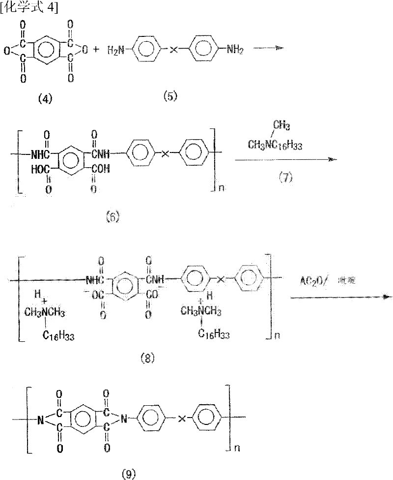
(式中,X表示C(C3H8-C6H4-C2H5)2。此外,n表示括弧内的重复构造的数目,是正整数。)(In the formula, X represents C(C 3 H 8 -C 6 H 4 -C 2 H 5 ) 2 . In addition, n represents the number of repeating structures in parentheses and is a positive integer.)
此外,作为氟化材料,使用下述化学式(10)所示的全氟聚醚(Perfluoropolyether,パ一フルオロポリエ一テル)(以下简称为PFPE),与上述说明的一样,利用LB法在玻璃基板和一对电极上形成了氟化膜。In addition, as a fluorinated material, a perfluoropolyether (Perfluoropolyether, パーフルリリロリエテル) (hereinafter referred to as PFPE) represented by the following chemical formula (10) was used, and as described above, the glass substrate was formed by the LB method. And a fluoride film is formed on a pair of electrodes.
[化学式5][chemical formula 5]

(式中,m、n表示括弧内的重复构造的数目,是正整数)。(In the formula, m and n represent the number of repeating structures in parentheses and are positive integers).
此外,此时准备了具备使聚酰亚胺材料(PI)与氟化材料(PFPE)的加入量分别不同、F原子的比例各自不同的各种高分子膜的基板。然后,与实施例1时一样制作液晶显示元件(实施例7~11)并测定了电压-透过率特性。下述表3是将各个液晶显示元件的结果整理而成的表。In addition, at this time, substrates provided with various polymer films in which the addition amounts of the polyimide material (PI) and the fluorinated material (PFPE) were different and the ratios of F atoms were different were prepared. Then, liquid crystal display elements (Examples 7 to 11) were produced in the same manner as in Example 1, and voltage-transmittance characteristics were measured. Table 3 below is a table in which the results of the respective liquid crystal display elements are sorted out.
[表3][table 3]
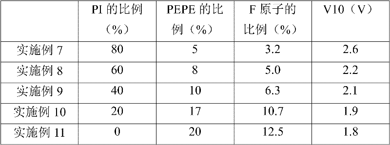
如表3所示,了解到阈值电压的值随着F原子的比例增加而降低,特别是在高分子材料的每个重复单元的F原子的比例为5重量%以上时(实施例8~11),显著地获得阈值电压降低的效果。进一步,了解到在每个重复单元的F原子的比例为10重量%以上时(实施例10、11),电压-透过率特性变得平缓,灰度等级显示性能良好。As shown in Table 3, it is understood that the value of the threshold voltage decreases as the ratio of F atoms increases, especially when the ratio of F atoms per repeating unit of the polymer material is 5% by weight or more (Examples 8-11 ), the effect of lowering the threshold voltage is remarkably obtained. Furthermore, it was found that when the proportion of F atoms per repeating unit was 10% by weight or more (Examples 10 and 11), the voltage-transmittance characteristics became flat, and the gray scale display performance was good.
实施方式4
实施方式4的液晶显示元件除了在设置在与液晶层的界面的对置基板一侧的高分子膜的表面具有纳米级的凹凸结构、和设置在与液晶层的界面的对置基板一侧的高分子膜的结构不同以外,具有与实施方式1的液晶显示元件相同的结构。In the liquid crystal display element of
具体而言,如下所述地制作了实施方式4的液晶显示元件。Specifically, the liquid crystal display element of
首先,准备对置基板一侧的玻璃基板,以2000eV的照射能量、照射时间120秒、照射角度45°的条件向该玻璃基板的表面照射离子束,形成深度50nm(RMS)、凹部间间距100nm的凹凸结构。另外,所谓的RMS是均方根(Root Mean Square)的简称,是平方并取算数平均,然后取平方根而计算出的值。First, a glass substrate on the counter substrate side is prepared, and an ion beam is irradiated on the surface of the glass substrate under the conditions of irradiation energy of 2000eV, irradiation time of 120 seconds, and irradiation angle of 45° to form a depth of 50nm (RMS) and a pitch of 100nm between recesses. concave-convex structure. In addition, the so-called RMS is the abbreviation of Root Mean Square (Root Mean Square), which is a value calculated by taking the arithmetic mean of the square, and then taking the square root.
接着,在玻璃基板的表面上形成包含实施方式2所使用的上述化学式(3)所示的化合物的化学吸附膜,然后使用与实施例6时相同的方法制作了液晶显示元件(实施例12)。Next, a chemical adsorption film containing the compound represented by the above chemical formula (3) used in
然后,同样对实施例12的液晶显示元件测定了电压-透过率特性,实施例12的液晶显示元件的V10为1.9V。这样,了解到在实施方式4中,不调整阵列基板而仅调整对置基板一侧就能够实现驱动电压的降低,实用价值极大。Then, the voltage-transmittance characteristics of the liquid crystal display element of Example 12 were measured similarly, and the V10 of the liquid crystal display element of Example 12 was 1.9V. In this way, in
另外,根据另外测定的结果,在表面具有上述凹凸结构的玻璃基板上形成的化学吸附膜与液晶层之间的临界表面能量为6.3N/m,另一方面,在具有平坦的表面的玻璃基板上形成的化学吸附膜与液晶层之间的临界表面能量为8.6N/m。由此可知,临界表面能量的降低、而且锚定能的降低成为阈值电压下降的主要原因。In addition, according to the results of separate measurements, the critical surface energy between the chemical adsorption film and the liquid crystal layer formed on the glass substrate having the above-mentioned concave-convex structure on the surface is 6.3 N/m. The critical surface energy between the chemical adsorption film and the liquid crystal layer formed on it is 8.6 N/m. From this, it can be seen that the decrease in the critical surface energy and the decrease in the anchor energy are the main causes of the decrease in the threshold voltage.
实施方式5
实施方式5的液晶显示元件除了使用无机取向膜OA-018(日产化学工业(株式会社)制造)作为设置在与液晶层的界面的高分子膜以外,具有与实施方式1的液晶显示元件相同的结构。在实施方式5,高分子膜包含含有SiO键的高分子材料。The liquid crystal display element of
除了使用上述材料作为高分子膜的材料以外,利用与实施例1时相同的方法制作液晶显示元件(实施例13),并同样测定电压-透过率特性,结果,V10=2.31V。A liquid crystal display element (Example 13) was produced in the same manner as in Example 1 except that the above materials were used as the material of the polymer film, and the voltage-transmittance characteristics were measured in the same manner. As a result, V10 = 2.31V.
另一方面,使用不含SiO键的有机取向膜SE-1211(日产化学工业(株式会社)制造)作为高分子膜的材料,利用与实施例1时相同的方法制作液晶显示元件(实施例2),并测定电压-透过率特性,结果,V10=2.73V。On the other hand, using the organic alignment film SE-1211 (manufactured by Nissan Chemical Industries (KK)) not containing SiO bonds as the material of the polymer film, a liquid crystal display element was produced by the same method as in Example 1 (Example 2 ), and measured voltage-transmittance characteristics, the result, V10 = 2.73V.
从该结果可知通过使用含有SiO键的材料作为高分子膜的材料,锚定能与通常的聚酰亚胺取向膜相比能够大幅减少,其结果是得到驱动电压的降低效果。From this result, it can be seen that by using a material containing SiO bonds as the material of the polymer film, the anchoring energy can be significantly reduced compared with a normal polyimide alignment film, and as a result, the driving voltage reduction effect can be obtained.
另外,与实施例1同样使用傅立叶变换红外分光法(FT-IR法)和X射线光电子能谱法(XPS法)对实施例13的液晶显示元件进行分析的结果,上述高分子材料所含有的每个重复单元的Si原子的比例为6.2重量%。In addition, as a result of analyzing the liquid crystal display element of Example 13 using Fourier transform infrared spectroscopy (FT-IR method) and X-ray photoelectron spectroscopy (XPS method) in the same manner as in Example 1, the polymer material contained in the above-mentioned The proportion of Si atoms per repeating unit was 6.2% by weight.
实施方式6
实施方式6的液晶显示元件除了设置在与液晶层的界面的高分子膜的结构不同以外,具有与实施方式1的液晶显示元件相同的结构。在实施方式6,高分子膜包含具有SiO键的高分子材料。The liquid crystal display element of
具体而言,如下所述地制作了实施方式6的液晶显示元件。Specifically, the liquid crystal display element of
首先,在乙醇52.3g和草酸20.5g的混合溶液中,在回流下滴下四乙氧基硅烷21.8g和十三氟辛基三甲氧基硅烷(TridecaFluoro-octyltrimethoxysilane,トリデカフルオロオクチルトリメトキシシラン)5.5g的混合物,并进行了5小时的回流。然后,加入丁基溶纤剂(Butyl-Cellosolve)75g,制作了具有4重量%的SiO2浓度的聚硅氧烷溶液。First, in a mixed solution of 52.3 g of ethanol and 20.5 g of oxalic acid, 21.8 g of tetraethoxysilane and 5.5 g of tridecafluorooctyltrimethoxysilane (Trideca Fluoro-octyltrimethoxysilane, tridecafluorooctyltrimethoxysilane) were dripped under reflux. g, and refluxed for 5 hours. Then, 75 g of butyl cellosolve (Butyl-Cellosolve) was added to prepare a polysiloxane solution having a SiO 2 concentration of 4% by weight.
接着,利用旋涂法在玻璃基板上将上述制作的聚硅氧烷成膜后,以60℃放置30分钟,然后以250℃烧制1小时,由此形成了高分子膜(取向膜)。干燥后的高分子膜的膜厚为100nm。然后,其他结构与实施例1时相同地制作液晶显示元件(实施例14),并在室温下测定了电压-透过率特性。其结果是,实施例14的液晶显示元件的V10为2.18V,确认获得了大幅的驱动电压的降低。Next, the above-prepared polysiloxane was formed into a film on a glass substrate by spin coating, left at 60° C. for 30 minutes, and then fired at 250° C. for 1 hour to form a polymer film (orientation film). The film thickness of the dried polymer film was 100 nm. Then, a liquid crystal display element (Example 14) was fabricated in the same manner as in Example 1 with other structures, and voltage-transmittance characteristics were measured at room temperature. As a result, V10 of the liquid crystal display element of Example 14 was 2.18V, and it was confirmed that a large driving voltage reduction was obtained.
另外,对实施例14的液晶显示元件的高分子膜进行化学分析的结果,上述高分子材料中含有的每个重复单元的Si含有量为约8重量%,由此,锚定能减少,驱动电压降低。由此,预测到阈值电压随着Si含有量变多而下降,从成膜性、取向性两方面的观点出发也优选为5~30重量%。In addition, as a result of chemical analysis of the polymer film of the liquid crystal display element of Example 14, the Si content per repeating unit contained in the polymer material was about 8% by weight, thereby reducing the anchoring energy and driving The voltage drops. From this, it is expected that the threshold voltage will decrease as the Si content increases, and it is preferably 5 to 30% by weight also from the viewpoints of film-formability and orientation.
实施方式7Embodiment 7
实施方式7的液晶显示元件除了在设置在与液晶层的界面的高分子膜的表面具有纳米级的凹凸结构和设置在与液晶层的界面的高分子膜的结构不同以外,具有与实施方式1的液晶显示元件相同的结构。The liquid crystal display element of Embodiment 7 has a structure different from that of
具体而言,如下所述地制作了实施方式7的液晶显示元件。Specifically, the liquid crystal display element of Embodiment 7 was produced as follows.
首先,准备玻璃基板,对该玻璃基板的表面照射聚焦离子束(照射时间120秒,照射角度45°),进行该玻璃基板的表面改性,形成深度为数十nm、凹部间间距为数十nm的凹凸结构。此处,使用凹凸结构的深度和间距的级别分别不同的多个玻璃基板,且其他结构与实施例1时一样地制作了在高分子膜的表面形成的凹凸结构的级别分别不同的多个液晶显示元件(实施例15~18,比较例3、4)。First, a glass substrate is prepared, and the surface of the glass substrate is irradiated with a focused ion beam (irradiation time 120 seconds, irradiation angle 45°) to modify the surface of the glass substrate to form a depth of tens of nm and a pitch of several tens of nanometers. nm concave-convex structure. Here, a plurality of glass substrates having different levels of depth and pitch of the uneven structure were used, and the other structures were the same as in Example 1, and a plurality of liquid crystals having different levels of the uneven structure formed on the surface of the polymer film were produced. Display elements (Examples 15 to 18, Comparative Examples 3 and 4).
对这些液晶显示元件使用与实施例1相同的方法在室温下测定电压-透过率特性后,得到了下述表4所示的结果。The voltage-transmittance characteristics of these liquid crystal display elements were measured at room temperature by the same method as in Example 1, and the results shown in Table 4 below were obtained.
[表4][Table 4]
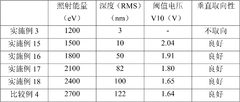
使用表面粗糙度计(商品名称:新视图(New View)5032,翟柯(ZYGO)公司制造)对各液晶显示元件(实施例15~18、比较例3、4)所具备的氮化硅(CNx)膜(高分子膜)表面进行观察的结果,观测到了纳米尺寸的微细的凹部和/或空孔。根据这样的形状效果,与表面平坦的有机取向膜相比能够得到小一位以上的锚定能。Using a surface roughness meter (trade name: New View (New View) 5032, manufactured by ZYGO Co.), the silicon nitride ( As a result of observing the surface of the CNx) film (polymer film), minute recesses and/or voids of nanometer size were observed. Due to such a shape effect, it is possible to obtain an anchor energy that is one digit or more smaller than that of an organic alignment film with a flat surface.
在上述的例子中,作为高分子膜的材料列举了氮化硅(CNx),但是并不仅限于此,还能够使用AlOx、SiOx、TiOx、HfOx、SiC、DLC(Diamondlike Carbon:类金刚石薄膜)等其他无机电介质。此外,在实施方式7,高分子膜可以为这些无机电介质的叠层膜,例如,能够将AlOx膜和HfOx膜重合等、适当地进行组合。In the above example, silicon nitride (CNx) was used as the material of the polymer film, but it is not limited to this, AlOx, SiOx, TiOx, HfOx, SiC, DLC (Diamondlike Carbon: diamond-like carbon film), etc. can also be used Other inorganic dielectrics. Furthermore, in Embodiment 7, the polymer film may be a laminated film of these inorganic dielectrics, for example, an AlOx film and an HfOx film may be stacked and combined appropriately.
在上述各实施例和比较例中,通过基板表面的微细凹凸的形状对液晶分子赋予垂直取向性,但是利用离子束照射的化学构造的变化(键能的减少)也有助于垂直取向性的提高。In each of the above-mentioned Examples and Comparative Examples, the liquid crystal molecules are given vertical alignment by the shape of the fine unevenness on the surface of the substrate, but the change of the chemical structure (reduction of bond energy) by ion beam irradiation also contributes to the improvement of the vertical alignment. .
另外,在基板表面的凹凸的深度不到10nm(比较例3)时未得到液晶分子的均匀的垂直取向性。此外,虽然即使超过100nm(比较例4)也得到良好的液晶分子的取向,但是由于阈值电压的降低效果饱和,因此实用上10nm以上、100nm以下为优选范围。In addition, when the depth of the irregularities on the substrate surface was less than 10 nm (Comparative Example 3), uniform vertical alignment of liquid crystal molecules was not obtained. In addition, even if it exceeds 100 nm (Comparative Example 4), good alignment of liquid crystal molecules is obtained, but since the effect of lowering the threshold voltage is saturated, 10 nm or more and 100 nm or less are practically preferable ranges.
以上对实施方式1~7进行了说明,但是各实施方式能够分别进行组合,此外,也可以使用将各高分子膜叠层而得的结构。进一步,在高分子膜中也可以含有Al(铝),Ga(镓)、In(铟)、Si(硅)、Ge(锗)、Sn(锡)、Ti(钛)、Zr(锆)、Hf(铪),由此能够更减少锚定能。
实施方式8
图13是表示实施方式8的液晶显示装置的结构的截面示意图。如图13所示,实施方式8的液晶显示装置包括具有液晶层3和夹持液晶层3的一对基板1、2的液晶显示面板,一对基板中的一个基板为阵列基板1,另一个为对置基板2。实施方式8的液晶显示元件除了在对置基板2一侧具有对置电极61以外具有与实施方式1的液晶显示元件相同的结构。如图13所示,在对置基板2一侧的透明基板(上基板)12的液晶层一侧的主面上,对置电极61、电介质层(绝缘层)62和高分子膜(取向膜)14依此顺序叠层。另外,也可以在对置电极61与透明基板12之间设置有彩色滤光片层。13 is a schematic cross-sectional view showing the structure of a liquid crystal display device according to
对置电极61由ITO、IZO等透明导电膜形成。对置电极61和电介质层62分别至少以覆盖整个显示区域的方式无缝隙地形成。在对置电极61被施加各图像元素共用的规定的电位。The
电介质层62由透明的绝缘材料形成。具体而言,由氮化硅等无机绝缘膜、丙烯酸树脂等有机绝缘膜等形成。The
另一方面,在阵列基板1一侧的透明基板11的液晶层13一侧的主面上,设置有包括图像元素电极30和共用电极40的梳型电极和高分子膜(取向膜)13。此外,在两个透明基板11、12的外主面上配置有偏光板17、18。On the other hand, comb electrodes including
除了黑显示时以外,在图像元素电极30与共用电极40之间以及在图像元素电极30与对置电极61之间施加不同的电压。共用电极40和对置电极61也可以接地,在共用电极40和对置电极61,既可以被施加相同大小和极性的电压,也可以被施加相互不同的大小和极性的电压。Different voltages are applied between the
实施方式8的液晶显示元件也能够以低阈值电压驱动。此外,通过形成对置电极61,能够提高响应速度。The liquid crystal display element of
图14是表示实施方式8的液晶显示装置的结构的平面示意图。另外,图14所示的方式的特征也可以适用于实施方式1~7。像素包括多个颜色的图像元素。不过,像素也可以不包括多个颜色的图像元素,即本实施方式的液晶显示元件也可以进行黑白显示,在这种情况下,以下的结构表示像素。此外,分别以正视液晶显示装置时、即正视一对基板面时的3点钟方向、12点钟方向、9点钟方向和6点钟方向为0°方向(方位)、90°方向(方位)、180°方向(方位)和270°方向(方位),以通过3点钟和9点钟的方向为左右方向,以通过12点钟和6点钟的方向为上下方向。14 is a schematic plan view showing the configuration of a liquid crystal display device according to
在透明基板11的液晶层3一侧的主面上设置有:信号线33;扫描线35;共用配线41;作为开关元件(有效(有源)元件)且在各图像元素各设置一个的薄膜晶体管(TFT)37;在各图像元素分别设置的图像元素电极30;和在多个图像元素(例如所有图像元素)共用地设置的共用电极40。On the main surface of the
扫描线35、共用配线41和共用电极40设置在透明基板12上,在扫描线35、共用配线41和共用电极40上设置有栅极绝缘膜(未图示),信号线33和图像元素电极30设置在栅极绝缘膜上,在信号线33和图像元素电极30上设置有高分子膜(取向膜)13。The scanning line 35, the common wiring 41 and the
另外,共用配线41、共用电极40和图像元素电极30利用光刻法在同一工序中使用相同的膜被图案形成,也可以配置在同一层(相同的绝缘膜)上。In addition, the common wiring 41, the
信号线33设置成相互平行的直线状,在相邻的图像元素间、在上下方向延伸。扫描线35设置成相互平行的直线状,在相邻的图像元素间、在左右方向延伸。信号线33与扫描线35正交,通过信号线33和扫描线35划分的区域大致成为一个图像元素区域。扫描线35在显示区域内也作为TFT37的栅极发挥作用。The signal lines 33 are provided in straight lines parallel to each other, and extend vertically between adjacent picture elements. The scanning lines 35 are arranged in straight lines parallel to each other, and extend in the left-right direction between adjacent picture elements. The signal line 33 is perpendicular to the scanning line 35 , and the area divided by the signal line 33 and the scanning line 35 roughly forms a picture element area. Scanning line 35 also functions as a gate of TFT 37 in the display region.
TFT37设置在信号线33和扫描线35的交叉部附近,包括在扫描线35上形成为岛状的半导体层38。此外,TFT37具有作为源极发挥作用的源极电极34和作为漏极发挥作用的漏极电极36。源极电极34连接TFT37与信号线33,漏极电极36连接TFT37与图像元素电极30。源极电极34和信号线33从相同的膜被图案形成且相互连接。漏极电极36和图像元素电极30从相同的膜被图案形成且相互连接。The TFT 37 is provided near the intersection of the signal line 33 and the scanning line 35 , and includes a semiconductor layer 38 formed in an island shape on the scanning line 35 . In addition, TFT 37 has source electrode 34 functioning as a source and drain electrode 36 functioning as a drain. The source electrode 34 is connected to the TFT 37 and the signal line 33 , and the drain electrode 36 is connected to the TFT 37 and the
对图像元素电极30,在TFT37为导通状态期间按规定的定时从信号线33供给图像信号。另一方面,对共用配线41和共用电极40,施加在各图像元素共用的规定的电位。To the
图像元素电极30的平面形状为梳齿形状,图像元素电极30具有直线状的主干部(图像元素主干部31)和直线状的多个梳齿部(图像元素梳齿部32)。图像元素主干部31沿着图像元素的短边(下边)设置。各图像元素梳齿部32与图像元素主干部31连接。此外,各图像元素梳齿部32从图像元素主干部31朝向相对的短边(上边)、即朝向大致90°方向延伸。The planar shape of the
共用电极40包含俯视梳齿形状具有直线状的多个梳齿部(共用梳齿部42)。共用梳齿部42和共用配线41从相同的膜被图案形成且相互连接。即,共用配线41也是连接多个共用梳齿部42彼此的共用电极40的主干部(共用主干部)。共用配线41与扫描线35平行地设置成直线状,在相邻的图像元素间、在左右方向延伸。共用梳齿部42从共用配线41朝向相对的图像元素的下边、即朝向大致270°方向延伸。The
这样,图像元素电极30和共用电极40以彼此的梳齿(图像元素梳齿部32、共用梳齿部42)咬合的方式相对配置。此外,图像元素梳齿部32和共用梳齿部42相互平行地配置,并且具有间隔地交错配置。In this way, the
此外,在图14所示的例子中,液晶分子的倾斜方向相反的两个畴在一个图像元素内形成。畴数并无特别限定,能够适当地设定,但是从得到良好的视角特性的观点出发,也可以在一个图像元素内形成四个畴。In addition, in the example shown in FIG. 14, two domains in which the inclination directions of the liquid crystal molecules are opposite are formed in one picture element. The number of domains is not particularly limited and can be appropriately set, but from the viewpoint of obtaining good viewing angle characteristics, four domains may be formed in one picture element.
此外,图14所示的例子具有在一个图像元素内电极间隔不同的两个以上的区域。更详细而言,在各图像元素内形成有电极间隔相对窄的区域(间隔Sn的区域)和电极间隔相对宽的区域(间隔Sw的区域)。由此,能够使各区域的VT特性的阈值不同,特别能够使低灰度等级的图像元素整体的VT特性的倾斜平稳(平缓)。其结果是,能够抑制泛白的产生,提高视角特性。另外,所谓的泛白是指在进行低灰度等级的比较暗的显示的状态下,在将观察方向从正面倒向倾斜时本应该看起来暗的显示看起来发白的现象。In addition, the example shown in FIG. 14 has two or more regions in which the electrode intervals differ within one picture element. More specifically, a region with a relatively narrow electrode interval (region with interval Sn) and a region with relatively wide electrode interval (region with interval Sw) are formed in each pixel. Thereby, the threshold value of the VT characteristic can be made different for each region, and the inclination of the VT characteristic of the entire low-gradation picture element can be stabilized (gentle). As a result, occurrence of whitening can be suppressed, and viewing angle characteristics can be improved. In addition, the so-called whitening refers to a phenomenon in which a display that should appear dark appears whitish when the viewing direction is tilted from the front in a state where a relatively dark display is performed at a low gradation level.
另外,本申请以2009年7月28日提出的日本专利申请2009-175704号和2010年1月15日提出的日本专利申请2010-006690号为基础,基于巴黎条约和所进入国家的法规主张优先权。该申请的所有内容均作为参照被引入本申请中。In addition, this application is based on Japanese Patent Application No. 2009-175704 filed on July 28, 2009 and Japanese Patent Application No. 2010-006690 filed on January 15, 2010, and claims priority based on the Treaty of Paris and the laws and regulations of the country where it entered. right. All content of this application is incorporated into this application by reference.
附图标记的说明Explanation of reference signs
1:阵列基板1: Array substrate
2:对置基板2: Counter substrate
3:液晶层3: Liquid crystal layer
11、12:透明基板11, 12: Transparent substrate
13、14:高分子膜(取向膜)13, 14: polymer film (orientation film)
15:液晶分子15: liquid crystal molecules
16:梳型电极16: Comb electrode
17、18:偏光板17, 18: polarizer
21:间隔物21: spacer
22:密封部件22: Sealing parts
30:图像元素电极30: Image element electrode
31:图像元素主干部31: image element backbone
32:图像元素梳齿部32: image element comb
33:信号线33: signal line
34:源极电极34: Source electrode
35:扫描线35: scan line
36:漏极电极36: Drain electrode
37:TFT37: TFT
38:半导体层38: Semiconductor layer
40:共用电极40: common electrode
41:共用配线(共用主干部)41: Shared wiring (shared trunk)
42:共用梳齿部42: shared comb
51:阵列基板一侧的偏光板的透过轴51: Transmission axis of the polarizer on the array substrate side
52:对置基板一侧的偏光板的透过轴52: Transmission axis of the polarizer on the opposing substrate side
53:电场的施加方位53: Applied orientation of electric field
61:对置电极61: Counter electrode
62:电介质层62: Dielectric layer
Claims (7)
Applications Claiming Priority (5)
| Application Number | Priority Date | Filing Date | Title |
|---|---|---|---|
| JP2009-175704 | 2009-07-28 | ||
| JP2009175704 | 2009-07-28 | ||
| JP2010006690 | 2010-01-15 | ||
| JP2010-006690 | 2010-01-15 | ||
| PCT/JP2010/053813 WO2011013396A1 (en) | 2009-07-28 | 2010-03-08 | Liquid crystal display element |
Publications (1)
| Publication Number | Publication Date |
|---|---|
| CN102472934A true CN102472934A (en) | 2012-05-23 |
Family
ID=43529063
Family Applications (1)
| Application Number | Title | Priority Date | Filing Date |
|---|---|---|---|
| CN2010800316752A Pending CN102472934A (en) | 2009-07-28 | 2010-03-08 | Liquid crystal display element |
Country Status (3)
| Country | Link |
|---|---|
| US (1) | US20120120363A1 (en) |
| CN (1) | CN102472934A (en) |
| WO (1) | WO2011013396A1 (en) |
Cited By (1)
| Publication number | Priority date | Publication date | Assignee | Title |
|---|---|---|---|---|
| CN106244170A (en) * | 2015-06-12 | 2016-12-21 | 三星显示有限公司 | LCD Monitor |
Families Citing this family (5)
| Publication number | Priority date | Publication date | Assignee | Title |
|---|---|---|---|---|
| WO2014167885A1 (en) * | 2013-04-12 | 2014-10-16 | Jsr株式会社 | Optical device |
| WO2020072087A1 (en) | 2018-10-04 | 2020-04-09 | Integra Lifesciences Corporation | Head wearable devices and methods |
| USD901737S1 (en) | 2018-10-04 | 2020-11-10 | Integra Lifesciences Corporation | Wearable headgear device |
| US10795226B2 (en) * | 2018-12-29 | 2020-10-06 | Wuhan China Star Optoelectronics Technology Co., Ltd. | Display device |
| JP2023146367A (en) * | 2022-03-29 | 2023-10-12 | シャープディスプレイテクノロジー株式会社 | Liquid crystal display device and method of controlling the liquid crystal display device |
Citations (5)
| Publication number | Priority date | Publication date | Assignee | Title |
|---|---|---|---|---|
| CN1321183A (en) * | 1999-07-05 | 2001-11-07 | 松下电器产业株式会社 | Thin film-forming chemisorbent substance, method for producing same, and use thereof |
| TW587191B (en) * | 1998-12-08 | 2004-05-11 | Fujitsu Display Tech | Liquid crystal display apparatus and liquid crystal display panel having wide transparent electrode and stripe electrodes |
| CN1591136A (en) * | 2003-09-04 | 2005-03-09 | 精工爱普生株式会社 | Inorganic orientation film forming method,inorganic orientation film,substrate for electronic device,liquid crystal panel and electronic apparatus |
| JP2008233412A (en) * | 2007-03-19 | 2008-10-02 | Stanley Electric Co Ltd | Liquid crystal display element |
| CN101470303A (en) * | 2007-12-26 | 2009-07-01 | 智索株式会社 | Liquid crystal tropism agent, liquid crystal tropism film and liquid crystal display element |
Family Cites Families (11)
| Publication number | Priority date | Publication date | Assignee | Title |
|---|---|---|---|---|
| JP4007373B2 (en) * | 1996-05-08 | 2007-11-14 | 株式会社日立製作所 | Active matrix type liquid crystal display device |
| JPH1184388A (en) * | 1997-09-16 | 1999-03-26 | Canon Inc | Liquid crystal element |
| JP2000111920A (en) * | 1998-09-30 | 2000-04-21 | Canon Inc | Liquid crystal element and method for manufacturing the liquid crystal element |
| JP4201942B2 (en) * | 1999-12-02 | 2008-12-24 | シャープ株式会社 | Liquid crystal display |
| US6642984B1 (en) * | 1998-12-08 | 2003-11-04 | Fujitsu Display Technologies Corporation | Liquid crystal display apparatus having wide transparent electrode and stripe electrodes |
| JP3099825B1 (en) * | 1999-10-12 | 2000-10-16 | 松下電器産業株式会社 | Liquid crystal display device and method of manufacturing the same |
| KR20020064295A (en) * | 1999-10-12 | 2002-08-07 | 마쯔시다덴기산교 가부시키가이샤 | Liquid crystal display element, optically anisotropic film, and methods for manufacturing them |
| US6900271B2 (en) * | 2002-05-31 | 2005-05-31 | Elsicon, Inc | Hybrid polymer materials for liquid crystal alignment layers |
| JP4671015B2 (en) * | 2003-12-17 | 2011-04-13 | Jsr株式会社 | Liquid crystal aligning agent and liquid crystal display element |
| JP4548727B2 (en) * | 2005-04-28 | 2010-09-22 | 大日本印刷株式会社 | Optical element in which liquid crystal molecules are homeotropically aligned, liquid crystal display device using the same, and liquid crystal display device |
| JP4605110B2 (en) * | 2006-07-11 | 2011-01-05 | セイコーエプソン株式会社 | Liquid crystal device and image display device including the same |
-
2010
- 2010-03-08 CN CN2010800316752A patent/CN102472934A/en active Pending
- 2010-03-08 WO PCT/JP2010/053813 patent/WO2011013396A1/en not_active Ceased
- 2010-03-08 US US13/387,205 patent/US20120120363A1/en not_active Abandoned
Patent Citations (5)
| Publication number | Priority date | Publication date | Assignee | Title |
|---|---|---|---|---|
| TW587191B (en) * | 1998-12-08 | 2004-05-11 | Fujitsu Display Tech | Liquid crystal display apparatus and liquid crystal display panel having wide transparent electrode and stripe electrodes |
| CN1321183A (en) * | 1999-07-05 | 2001-11-07 | 松下电器产业株式会社 | Thin film-forming chemisorbent substance, method for producing same, and use thereof |
| CN1591136A (en) * | 2003-09-04 | 2005-03-09 | 精工爱普生株式会社 | Inorganic orientation film forming method,inorganic orientation film,substrate for electronic device,liquid crystal panel and electronic apparatus |
| JP2008233412A (en) * | 2007-03-19 | 2008-10-02 | Stanley Electric Co Ltd | Liquid crystal display element |
| CN101470303A (en) * | 2007-12-26 | 2009-07-01 | 智索株式会社 | Liquid crystal tropism agent, liquid crystal tropism film and liquid crystal display element |
Cited By (1)
| Publication number | Priority date | Publication date | Assignee | Title |
|---|---|---|---|---|
| CN106244170A (en) * | 2015-06-12 | 2016-12-21 | 三星显示有限公司 | LCD Monitor |
Also Published As
| Publication number | Publication date |
|---|---|
| WO2011013396A1 (en) | 2011-02-03 |
| US20120120363A1 (en) | 2012-05-17 |
Similar Documents
| Publication | Publication Date | Title |
|---|---|---|
| CN102282506B (en) | Liquid crystal display device | |
| JP5190818B2 (en) | Liquid crystal device and method for manufacturing liquid crystal device | |
| US8330890B2 (en) | Display device | |
| US8120746B2 (en) | Display panel and display device having medium whose optical anisotropy magnitude changes according to electric field | |
| CN100381887C (en) | Display elements and display devices | |
| CN102317849B (en) | Liquid crystal display device | |
| CN102414608A (en) | Liquid crystal panel and liquid crystal display device | |
| US7876385B2 (en) | Liquid crystal device | |
| CN102472934A (en) | Liquid crystal display element | |
| JP2015179100A (en) | liquid crystal display device | |
| Chaudhary et al. | Liquid crystals alignment with PbS nanosculptured thin films | |
| EP2437111A1 (en) | Liquid crystal panel, method for manufacturing same, and liquid crystal display device | |
| US8111358B2 (en) | Dispay panel and display apparatus | |
| CN102472926A (en) | Liquid crystal display element | |
| CN1708724A (en) | Multi-domain vertical alignment liquid crystal display | |
| EP1962131B1 (en) | Liquid crystal device | |
| KR101682433B1 (en) | Liquid crystal display device | |
| WO2012011443A1 (en) | Liquid crystal panel and liquid crystal display device | |
| CN1350196A (en) | Wide-viewing angle liquid crystal display | |
| CN102047175B (en) | Liquid crystal panel and liquid crystal display device | |
| Kim et al. | 13‐3: Development of High‐performance TFT‐LCDs using Optically‐Isotropic Nano‐size Encapsulated Liquid Crystals | |
| JPH095754A (en) | Liquid crystal display element | |
| TW548490B (en) | Improvements in liquid crystal displays | |
| US7733452B2 (en) | Materials for promoting alignment of liquid crystals on SiOx and other substrates | |
| TW201222075A (en) | Bistable liquid crystal device |
Legal Events
| Date | Code | Title | Description |
|---|---|---|---|
| C06 | Publication | ||
| PB01 | Publication | ||
| C10 | Entry into substantive examination | ||
| SE01 | Entry into force of request for substantive examination | ||
| C02 | Deemed withdrawal of patent application after publication (patent law 2001) | ||
| WD01 | Invention patent application deemed withdrawn after publication |
Application publication date: 20120523 |