CN102448249B - Method for manufacturing double-sided circuit board - Google Patents
Method for manufacturing double-sided circuit board Download PDFInfo
- Publication number
- CN102448249B CN102448249B CN201010508604.9A CN201010508604A CN102448249B CN 102448249 B CN102448249 B CN 102448249B CN 201010508604 A CN201010508604 A CN 201010508604A CN 102448249 B CN102448249 B CN 102448249B
- Authority
- CN
- China
- Prior art keywords
- copper
- foil layer
- copper foil
- double
- ring
- Prior art date
- Legal status (The legal status is an assumption and is not a legal conclusion. Google has not performed a legal analysis and makes no representation as to the accuracy of the status listed.)
- Active
Links
- 238000004519 manufacturing process Methods 0.000 title claims abstract description 40
- 238000000034 method Methods 0.000 title claims abstract description 30
- RYGMFSIKBFXOCR-UHFFFAOYSA-N Copper Chemical compound [Cu] RYGMFSIKBFXOCR-UHFFFAOYSA-N 0.000 claims abstract description 168
- 239000011889 copper foil Substances 0.000 claims abstract description 102
- 239000000853 adhesive Substances 0.000 claims abstract description 85
- 230000001070 adhesive effect Effects 0.000 claims abstract description 85
- 239000010410 layer Substances 0.000 claims description 132
- 239000012790 adhesive layer Substances 0.000 claims description 20
- 238000003825 pressing Methods 0.000 claims description 15
- 239000002390 adhesive tape Substances 0.000 claims description 7
- 238000010030 laminating Methods 0.000 claims description 5
- 238000004026 adhesive bonding Methods 0.000 claims 24
- 230000004888 barrier function Effects 0.000 claims 6
- 230000015572 biosynthetic process Effects 0.000 claims 6
- 229920000297 Rayon Polymers 0.000 claims 2
- 150000001875 compounds Chemical class 0.000 claims 2
- 239000003292 glue Substances 0.000 claims 2
- 238000003466 welding Methods 0.000 claims 1
- 229910052802 copper Inorganic materials 0.000 abstract description 66
- 239000010949 copper Substances 0.000 abstract description 66
- 238000010586 diagram Methods 0.000 description 14
- 238000009713 electroplating Methods 0.000 description 9
- 229920002120 photoresistant polymer Polymers 0.000 description 8
- 230000002093 peripheral effect Effects 0.000 description 6
- 238000007747 plating Methods 0.000 description 6
- 238000005520 cutting process Methods 0.000 description 2
- 238000011161 development Methods 0.000 description 2
- 238000005530 etching Methods 0.000 description 2
- 239000011888 foil Substances 0.000 description 2
- 238000009413 insulation Methods 0.000 description 2
- 238000003475 lamination Methods 0.000 description 2
- 238000012986 modification Methods 0.000 description 2
- 230000004048 modification Effects 0.000 description 2
- 229910000679 solder Inorganic materials 0.000 description 2
- 239000000758 substrate Substances 0.000 description 2
- 230000037303 wrinkles Effects 0.000 description 2
- 238000012512 characterization method Methods 0.000 description 1
- 238000005553 drilling Methods 0.000 description 1
- 238000005516 engineering process Methods 0.000 description 1
- PCHJSUWPFVWCPO-UHFFFAOYSA-N gold Chemical compound [Au] PCHJSUWPFVWCPO-UHFFFAOYSA-N 0.000 description 1
- 229910052737 gold Inorganic materials 0.000 description 1
- 239000010931 gold Substances 0.000 description 1
- 239000011810 insulating material Substances 0.000 description 1
- 239000000463 material Substances 0.000 description 1
- 238000000465 moulding Methods 0.000 description 1
- 230000003647 oxidation Effects 0.000 description 1
- 238000007254 oxidation reaction Methods 0.000 description 1
- 238000007639 printing Methods 0.000 description 1
- 230000001681 protective effect Effects 0.000 description 1
- 238000004381 surface treatment Methods 0.000 description 1
Images


Landscapes
- Production Of Multi-Layered Print Wiring Board (AREA)
Abstract
一种双面电路板的制作方法,包括步骤:提供第一覆铜板和第二覆铜板,第一覆铜板包括第一铜箔层和第二铜箔层,第二覆铜板包括第三铜箔层和第四铜箔层;在第一铜箔层制作形成第一线路图形,在第三铜箔层制作形成第三线路图形;在第一铜箔层贴合第一胶粘环,在第三铜箔层贴合第二胶粘环;提供支撑板,其具有第一支撑面和第二支撑面;将第一覆铜板通过第一胶粘环粘贴并压合于第一支撑面,将第二覆铜板通过第二胶粘环粘贴并压合于第二支撑面;在第二铜箔层制作形成第二线路图形,从而将第一覆铜板制成第一双面板,并在第四铜箔层制作形成第四线路图形,从而将第二覆铜板制成第二双面板;将第一双面板与第一胶粘环分离,将第二双面板与第二胶粘环分离。
A method for manufacturing a double-sided circuit board, comprising the steps of: providing a first copper-clad laminate and a second copper-clad laminate, the first copper-clad laminate includes a first copper foil layer and a second copper foil layer, and the second copper-clad laminate includes a third copper foil layer and the fourth copper foil layer; the first circuit pattern is formed on the first copper foil layer, and the third circuit pattern is formed on the third copper foil layer; the first adhesive ring is pasted on the first copper foil layer, and the The three copper foil layers are attached to the second adhesive ring; a support plate is provided, which has a first support surface and a second support surface; the first copper clad laminate is pasted and pressed on the first support surface through the first adhesive ring, and the The second copper-clad laminate is pasted and pressed on the second support surface through the second adhesive ring; the second circuit pattern is formed on the second copper foil layer, so that the first copper-clad laminate is made into the first double-sided board, and on the fourth The copper foil layer is manufactured to form a fourth circuit pattern, so that the second copper clad laminate is made into a second double-sided board; the first double-sided board is separated from the first adhesive ring, and the second double-sided board is separated from the second adhesive ring.
Description
技术领域 technical field
本发明涉及电路板制作技术,特别涉及一种双面电路板的制作方法。The invention relates to circuit board manufacturing technology, in particular to a method for manufacturing a double-sided circuit board.
背景技术 Background technique
一般地,电路板由覆铜板经裁切、钻孔、曝光、显影、蚀刻、压合、印刷、成型等一系列工艺制作而成。具体可参阅C.H.Steer等人在Proceedings ofthe IEEE,Vol.39,No.2(2002年8月)中发表的“Dielectric characterization ofprinted circuit board substrates”一文。Generally, circuit boards are made of copper clad laminates through a series of processes such as cutting, drilling, exposure, development, etching, pressing, printing, and molding. For details, please refer to the article "Dielectric characterization of printed circuit board substrates" published by C.H.Steer et al. in Proceedings of the IEEE, Vol.39, No.2 (August 2002).
随着电路板的发展,其对高挠折性及轻薄性的要求越来越高。目前,用于制作双面印刷电路板的覆铜板的厚度已经由原来的60微米下降到36微米,甚至达到27微米。由于覆铜板的厚度太薄,在现有设备上使用该种只有27微米或36微米的覆铜板制作双面电路板时,其良率很低。在制作过程中,主要存在以下问题:一是覆铜板在湿制程中容易被弯折压伤;二是在选择性电镀后覆铜板发生卷曲,难于剥离选择性电镀覆盖膜,甚至可能在剥离时造成双面电路板报废;三是在利用电镀夹具夹持该覆铜板进行电镀时,由于其厚度太薄难于夹紧,在电镀过程中容易滑落电镀液中,造成双面电路板报废;四是在制作第二面的导电线路时,由于覆铜基板太薄且过软,蚀刻第二面的导电线路后得到的双面电路板产生严重的皱折,影响产品外观以及厚度防焊保护膜的压合制作。With the development of circuit boards, the requirements for high flexibility and thinness are getting higher and higher. At present, the thickness of copper-clad laminates used to make double-sided printed circuit boards has dropped from 60 microns to 36 microns, and even reached 27 microns. Because the thickness of the copper clad laminate is too thin, when the copper clad laminate with only 27 microns or 36 microns is used to make double-sided circuit boards on existing equipment, the yield rate is very low. In the production process, there are mainly the following problems: first, the copper clad laminate is easily bent and crushed during the wet process; second, the copper clad laminate is curled after selective electroplating, making it difficult to peel off the selective plating covering film, and may even be damaged during peeling. Cause the double-sided circuit board to be scrapped; the third is that when the copper-clad board is clamped by the electroplating fixture for electroplating, because its thickness is too thin to be clamped, it is easy to slip into the electroplating solution during the electroplating process, causing the double-sided circuit board to be scrapped; the fourth is When making the conductive circuit on the second side, because the copper-clad substrate is too thin and too soft, the double-sided circuit board obtained after etching the conductive circuit on the second side has serious wrinkles, which affects the appearance of the product and the thickness of the solder mask film. Lamination production.
因此,针对上述问题,有必要提供一种可有效提高良率并减少皱折的双面电路板的制作方法。Therefore, in view of the above problems, it is necessary to provide a method for manufacturing a double-sided circuit board that can effectively improve yield and reduce wrinkles.
发明内容 Contents of the invention
下面将以具体实施例说明一种双面电路板的制作方法。A method for manufacturing a double-sided circuit board will be described below with a specific embodiment.
一种双面电路板的制作方法,包括步骤:提供第一覆铜板和第二覆铜板,该第一覆铜板包括第一绝缘层以及分别形成于该第一绝缘层相对两表面的第一铜箔层和第二铜箔层,该第一覆铜板具有第一线路区和围绕第一线路区的第一边缘区,该第二覆铜板包括第二绝缘层以及分别形成于该第二绝缘层相对两表面的第三铜箔层和第四铜箔层,该第二覆铜板具有第二线路区和围绕第二线路区的第二边缘区;在第一铜箔层的第一线路区制作形成第一线路图形,在第三铜箔层的第二线路区制作形成第三线路图形;在第一铜箔层的第一边缘区贴合形成一个环状的第一胶粘环,在第三铜箔层的第二边缘区贴合形成一个环状的第二胶粘环;提供支撑板,该支撑板具有相对的第一支撑面和第二支撑面;将该第一覆铜板通过第一胶粘环以第一压合温度粘贴并压合于第一支撑面,将该第二覆铜板通过第二胶粘环以第一压合温度粘贴并压合于第二支撑面;在第二铜箔层的第一线路区制作形成第二线路图形,从而将第一覆铜板制成第一双面板,并在第四铜箔层的第二线路区制作形成第四线路图形,从而将第二覆铜板制成第二双面板;以及将该第一双面板与第一胶粘环分离,将第二双面板与第二胶粘环分离。A method for manufacturing a double-sided circuit board, comprising the steps of: providing a first copper-clad laminate and a second copper-clad laminate, the first copper-clad laminate comprising a first insulating layer and first copper layers respectively formed on opposite surfaces of the first insulating layer A foil layer and a second copper foil layer, the first copper clad board has a first line area and a first edge area surrounding the first line area, the second copper clad board includes a second insulating layer and is respectively formed on the second insulating layer Relative to the third copper foil layer and the fourth copper foil layer on both surfaces, the second copper clad laminate has a second circuit area and a second edge area surrounding the second circuit area; the first circuit area of the first copper foil layer is made Form the first circuit pattern, make and form the third circuit pattern in the second circuit area of the third copper foil layer; bond the first edge area of the first copper foil layer to form a ring-shaped first adhesive ring, and The second edge regions of the three copper foil layers are laminated to form a ring-shaped second adhesive ring; a support plate is provided, and the support plate has a first support surface and a second support surface opposite; the first copper clad laminate is passed through the second An adhesive ring is pasted and pressed on the first supporting surface at the first pressing temperature, and the second copper clad laminate is pasted and pressed on the second supporting surface at the first pressing temperature through the second adhesive ring; The first circuit area of the second copper foil layer is fabricated to form a second circuit pattern, so that the first copper-clad laminate is made into a first double-sided board, and a fourth circuit pattern is formed in the second circuit area of the fourth copper foil layer, thereby making the The second copper-clad laminate is made into a second double-sided board; and the first double-sided board is separated from the first adhesive ring, and the second double-sided board is separated from the second adhesive ring.
相对于现有技术,本技术方案的双面电路板的制作方法,其在第一覆铜板的第一铜箔层、第二覆铜板的第三铜箔层分别制作形成第一线路图形、第三线路图形后,再将第一覆铜板、第二覆铜板分别通过第一胶粘环、第二胶粘环分别粘贴并压合至支撑板的第一支撑面与第二支撑面,然后在第一覆铜板的第二铜箔层、第二覆铜板的第四铜箔层分别制作形成第二线路图形、第四线路图形,最后分离得到制作好的第一双面板和第二双面板作为两个双面电路板,由于采用第一胶粘环与第二胶粘环分别将第一覆铜板、第二覆铜板粘贴并压合至支撑板的第一支撑面与第二支撑面,从而可避免第一覆铜板与第二覆铜板在分别制作形成第二线路图形、第四线路图形的湿制程制作中被弯折压伤并产生严重皱折,并且便于剥离在制作形成第二线路图形、第四线路图形时采用的光致抗蚀剂,进而提升薄型化的双面电路板的制作效率。Compared with the prior art, the method for making a double-sided circuit board of this technical solution is to form a first circuit pattern, a second circuit pattern, and a second circuit pattern on the first copper foil layer of the first copper-clad laminate and the third copper foil layer of the second copper-clad laminate, respectively. After the three-line pattern, the first copper-clad laminate and the second copper-clad laminate are pasted and pressed to the first support surface and the second support surface of the support plate through the first adhesive ring and the second adhesive ring respectively, and then The second copper foil layer of the first copper-clad laminate and the fourth copper foil layer of the second copper-clad laminate are respectively manufactured to form the second circuit pattern and the fourth circuit pattern, and finally the prepared first double-sided board and the second double-sided board are separated as Two double-sided circuit boards, since the first copper clad laminate and the second copper clad laminate are pasted and pressed to the first support surface and the second support surface of the support plate by using the first adhesive ring and the second adhesive ring respectively, thus It can prevent the first copper-clad laminate and the second copper-clad laminate from being bent, crushed and severely wrinkled during the wet process of forming the second circuit pattern and the fourth circuit pattern respectively, and it is easy to peel off to form the second circuit pattern , The photoresist used in the fourth circuit pattern, thereby improving the production efficiency of the thin double-sided circuit board.
附图说明 Description of drawings
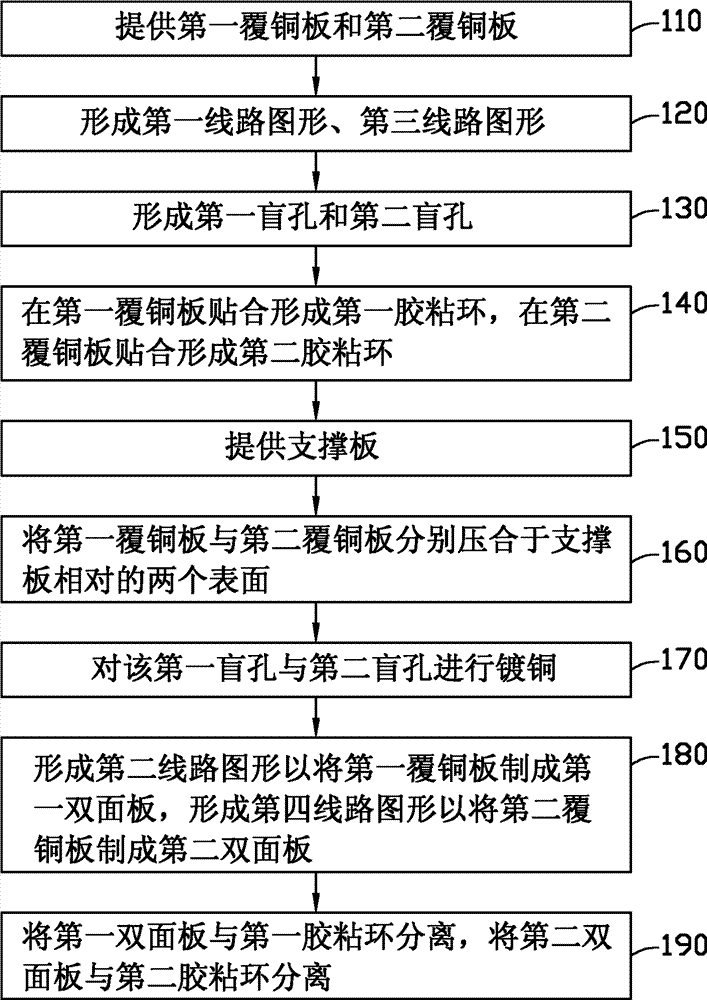
图1是本技术方案实施例提供的双面电路板的制作方法的流程图。Fig. 1 is a flowchart of a method for manufacturing a double-sided circuit board provided by an embodiment of the technical solution.
图2是图1的双面电路板的制作方法中提供的第一覆铜板和第二覆铜板的示意图。FIG. 2 is a schematic diagram of the first copper-clad laminate and the second copper-clad laminate provided in the manufacturing method of the double-sided circuit board in FIG. 1 .
图3是图1的双面电路板的制作方法中在第一覆铜板上形成第一线路图形以及在第二覆铜板上形成第三线路图形的示意图。3 is a schematic diagram of forming a first circuit pattern on the first copper clad board and forming a third circuit pattern on the second copper clad board in the manufacturing method of the double-sided circuit board in FIG. 1 .
图4是图1的双面电路板的制作方法中在第一覆铜板上形成第一盲孔以及在第二覆铜板上形成第二盲孔的示意图。FIG. 4 is a schematic diagram of forming a first blind hole on a first copper clad board and forming a second blind hole on a second copper clad board in the manufacturing method of a double-sided circuit board in FIG. 1 .
图5是图1的双面电路板的制作方法中粘贴有第一胶粘环的第一覆铜板以及粘贴有第二胶粘环的第二覆铜板的示意图。5 is a schematic diagram of the first copper clad laminate pasted with the first adhesive ring and the second copper clad laminate pasted with the second adhesive ring in the manufacturing method of the double-sided circuit board in FIG. 1 .
图6是图1的双面电路板的制作方法中提供的第一胶粘片和第二胶粘片的示意图。FIG. 6 is a schematic diagram of the first adhesive sheet and the second adhesive sheet provided in the manufacturing method of the double-sided circuit board in FIG. 1 .
图7是图1的双面电路板的制作方法中提供的裁切掉中间区域的第一胶粘片和第二胶粘片的示意图。FIG. 7 is a schematic diagram of the first adhesive sheet and the second adhesive sheet with the middle area cut off provided in the manufacturing method of the double-sided circuit board in FIG. 1 .
图8是图1的双面电路板的制作方法中提供的第一离型胶带和第二离型胶带的示意图。FIG. 8 is a schematic diagram of the first release tape and the second release tape provided in the manufacturing method of the double-sided circuit board in FIG. 1 .
图9是图1的双面电路板的制作方法中粘贴有第一离型胶带的第一覆铜板以及粘贴有第二离型胶带的第二覆铜板的示意图。9 is a schematic diagram of the first copper clad laminate pasted with the first release tape and the second copper clad laminate pasted with the second release tape in the manufacturing method of the double-sided circuit board in FIG. 1 .
图10是图1的双面电路板的制作方法中提供的支撑板的示意图。FIG. 10 is a schematic diagram of a support plate provided in the manufacturing method of the double-sided circuit board in FIG. 1 .
图11是图1的双面电路板的制作方法中将第一覆铜板与第二覆铜板压合于支撑板的示意图。FIG. 11 is a schematic diagram of pressing the first copper-clad laminate and the second copper-clad laminate to the support plate in the manufacturing method of the double-sided circuit board in FIG. 1 .
图12是图7沿I-I方向的剖视图。Fig. 12 is a sectional view along the I-I direction of Fig. 7 .
图13是图1的双面电路板的制作方法中对第一盲孔与第二盲孔进行镀铜的示意图。FIG. 13 is a schematic diagram of copper plating on the first blind hole and the second blind hole in the manufacturing method of the double-sided circuit board in FIG. 1 .
图14是图1的双面电路板的制作方法中在第一覆铜板上制作形成第二线路图形的示意图。FIG. 14 is a schematic diagram of forming a second circuit pattern on the first copper-clad laminate in the method for manufacturing the double-sided circuit board in FIG. 1 .
图15是图1的双面电路板的制作方法中在第二覆铜板上制作形成第四线路图形的示意图。FIG. 15 is a schematic diagram of forming a fourth circuit pattern on the second copper clad laminate in the manufacturing method of the double-sided circuit board in FIG. 1 .
图16是图1的双面电路板的制作方法中将第一双面板、第二双面板板分别与第一胶粘环、第二胶粘环分离的示意图。FIG. 16 is a schematic diagram of separating the first double-sided board and the second double-sided board from the first adhesive ring and the second adhesive ring respectively in the manufacturing method of the double-sided circuit board in FIG. 1 .
主要元件符号说明Description of main component symbols
第一覆铜板 10The first
第二覆铜板 20Second
第一绝缘层 12
第一铜箔层 14The first
第二铜箔层 16Second
第一线路区 101The
第一边缘区 102First Fringe District 102
第二绝缘层 22
第三铜箔层 24The third
第四铜箔层 26The fourth
第二线路区 201
第二边缘区 202
第一线路图形 142First Line
第二线路图形 162
第三线路图形 242
第四线路图形 262
第一盲孔 104The first
第二盲孔 204Second
第一胶粘环 310First
第二胶粘环 320Second
第一胶粘片 31First Adhesive Sheet 31
第二胶粘片 32Second adhesive sheet 32
中央区域 311、321Central Area 311, 321
周边区域 312、322
第一离型胶带 41The
第二离型胶带 42
第一胶粘层 411First
第一离型层 412The
第二胶粘层 421Second
第二离型层 422The
支撑板 50
第一支撑面 51The
第二支撑面 52
第一封闭空间 301The first enclosed space 301
第二封闭空间 302Second enclosed space 302
具体实施方式 Detailed ways
下面将结合附图和实施例对本技术方案的双面电路板制作方法作进一步详细说明。The method for manufacturing the double-sided circuit board of the technical solution will be further described in detail below in conjunction with the drawings and embodiments.
请参阅图1,本技术方案实施例提供一种双面电路板制作方法,其包括以下步骤:Please refer to Fig. 1, the embodiment of this technical solution provides a kind of double-sided circuit board manufacturing method, and it comprises the following steps:
步骤110,请参阅图2,提供第一覆铜板10和第二覆铜板20。该第一覆铜板10包括第一绝缘层12以及分别形成于该第一绝缘层12相对两表面的第一铜箔层14和第二铜箔层16。该第一覆铜板10具有第一线路区101和围绕该第一线路区101的第一边缘区102。该第二覆铜板20包括第二绝缘层22以及分别形成于该第二绝缘层22相对两表面的第三铜箔层24和第四铜箔层26。该第二覆铜板20具有第二线路区201和围绕该第二线路区201的第二边缘区202。
具体地,该第一边缘区102位于该第一线路区101的外侧。该第一线路区101为最终形成电路板成品的区域,该第一边缘区102为形成电路板成品时需切割去除的区域。本实施例中,该第一覆铜板10的厚度可为27微米或者36微米。当该第一覆铜板10的厚度为27微米时,该第一绝缘层12、第一铜箔层14以及第二铜箔层16的厚度均为9微米。当该第一覆铜板10的厚度为36微米时,该第一绝缘层12、第一铜箔层14以及第二铜箔层16的厚度均为12微米。Specifically, the
该第二边缘区202位于该第二线路区201的外侧。该第二边缘区202与第一边缘区102相对应,该第二线路区201与第一线路区101相对应。该第二线路区201为最终形成电路板成品的区域,该第二边缘区202为形成电路板成品时需切割去除的区域。本实施例中,该第二覆铜板20的厚度可为27微米或者36微米。当该第二覆铜板20的厚度为27微米时,该第二绝缘层22、第三铜箔层24以及第四铜箔层26的厚度均为9微米。当该第二覆铜板20的厚度为36微米时,该第二绝缘层22、第三铜箔层24以及第四铜箔层26的厚度均为12微米。The
步骤120,请参阅图3,在第一铜箔层14的第一线路区101制作形成第一线路图形142,在第三铜箔层24的第二线路区201制作形成第三线路图形242。
具体地,在第一覆铜板10的第一铜箔层14上制作形成第一线路图形142包括以下步骤:首先,在第一铜箔层14表面覆盖光致抗蚀剂(图未示);接着,利用与该第一线路图形142具有对应图案的光掩膜(图未示)对该光致抗蚀剂进行曝光;然后,利用显影液去掉该光致抗蚀剂被曝光的部分区域;最后,利用蚀刻液对该第一铜箔层14进行蚀刻并形成第一线路图形142。该第一线路图形142位于第一覆铜板10的第一线路区101。Specifically, making and forming the
类似地,在第二覆铜板20的第三铜箔层24上制作形成第三线路图形242的具体步骤与上述第一线路图形142的形成步骤基本相同,在此不再赘述。该第三线路图形242位于第二覆铜板20的第二线路区201。Similarly, the specific steps of forming the
步骤130,请参阅图4,在第一线路区101形成第一盲孔104,该第一盲孔104穿透该第二铜箔层16与第一绝缘层12,在第二线路区201形成第二盲孔204,该第二盲孔204穿透该第四铜箔层26与第二绝缘层22。
具体地,可利用激光自第二铜箔层16所在的一侧对第二铜箔层16与第一绝缘层12进行烧蚀以形成穿透该第二铜箔层16与第一绝缘层12的第一盲孔104。该第一盲孔104位于第一覆铜板10的第一线路区101。并可利用激光自第四铜箔层26所在的一侧对第四铜箔层26与第二绝缘层22进行烧蚀以形成穿透该第四铜箔层26与第二绝缘层22的第二盲孔204。该第二盲孔204位于第二覆铜板20的第二线路区201。Specifically, a laser can be used to ablate the second
可以理解的是,在第一覆铜板10与第二覆铜板20不需要形成盲孔时,该步骤130也可省略。It can be understood that this
步骤140,请参阅图5,在第一铜箔层14的第一边缘区102贴合形成一个环状的第一胶粘环310,在第三铜箔层24的第二边缘区202贴合形成一个环状的第二胶粘环320。优选地,该第二胶粘环320与第一胶粘环310相对齐。
具体地,在一个实施例中,在第一铜箔层14的第一边缘区102贴合形成一个环状的第一胶粘环310包括以下步骤:首先,请参阅图6,提供第一胶粘片31,所述第一胶粘片31具有中央区域311和围绕中央区域311的周边区域312。接着,请参阅图7,裁切去除第一胶粘片31的中央区域311,从而获得第一胶粘片31的周边区域312。然后,将第一胶粘片31的周边区域312贴合于第一铜箔层14的第一边缘区102,从而形成如图5所示的第一胶粘环310。Specifically, in one embodiment, attaching and forming an annular first
类似地,在第三铜箔层24的第二边缘区202贴合形成一个环状的第二胶粘环320包括以下步骤:首先,请参阅图6,提供第二胶粘片32,所述第二胶粘片32具有中央区域321和围绕中央区域321的周边区域322。接着,请参阅图7,裁切去除第二胶粘片32的中央区域321,从而获得第二胶粘片32的周边区域322。然后,将第二胶粘片32的周边区域322贴合于第三铜箔层24的第二边缘区202,从而形成如图5所示的第二胶粘环320。Similarly, laminating and forming an annular second
当然,该第一胶粘环310与第二胶粘环320也可采用其他方法分别粘贴形成于第一铜箔层14的第一边缘区102与第三铜箔层24的第二边缘区202。例如,在另一个实施例中,在第一铜箔层14的第一边缘区102贴合形成一个环状的第一胶粘环310包括以下步骤:首先,请参阅图8,提供第一离型胶带41,该第一离型胶带41包括第一胶粘层411和第一离型层412。该第一离型层412贴在该第一胶粘层411的一个表面。当然,该第一胶粘层411的另一个表面也可贴有离型层(图未示)以保护未粘贴之前的第一胶粘层411,在贴合时再剥离该离型层。接着,请参阅图9,将第一离型胶带41环绕第一线路区101贴合于第一边缘区102,并使第一胶粘层411与第一铜箔层14接触。然后,去除第一离型层412,从而获得由第一离型胶带41的第一胶粘层411构成的如图5所示的第一胶粘环310。Certainly, the first
类似地,在第三铜箔层24的第二边缘区202贴合形成一个环状的第二胶粘环320包括以下步骤:首先,请参阅图8,提供第二离型胶带42,该第二离型胶带42包括第二胶粘层421和第二离型层422。该第二离型层422贴在该第二胶粘层421的一个表面。当然,该第二胶粘层421的另一个表面也可贴有离型层(图未示)以保护未粘贴之前的第二胶粘层421,在贴合时再剥离该离型层。接着,请参阅图9,将第二离型胶带42环绕第二线路区201贴合于第二边缘区202,并使第二胶粘层421与第三铜箔层24接触。然后,去除第二离型层422,从而获得由第二离型胶带42的第二胶粘层421构成的如图5所示的第二胶粘环320。Similarly, attaching and forming an annular second
步骤150,请参阅图10,提供支撑板50,该支撑板50具有相对的第一支撑面51和第二支撑面52。
该支撑板50可选用硬质绝缘材料制作形成,且其具有较好的热化学稳定性以及较高的强度。本实施例中,该支撑板50表面的面积大小与上述第一覆铜板10、第二覆铜板20的表面的面积大小基本相等。The
步骤160,请参阅图11及图12,将第一覆铜板10通过第一胶粘环310以第一压合温度粘贴并压合于第一支撑面51,将第二覆铜板20通过第二胶粘环320以第一压合温度粘贴并压合于第二支撑面52。
此时,第一覆铜板10的第一铜箔层14与该第一支撑面51相对,该环状的第一胶粘环310将第一铜箔层14的第一线路区101与外界环境隔绝。由于第一胶粘环310压合后并无粘到第一铜箔层14的第一线路区101,从而不会影响或破坏第一线路区101中的第一线路图形142。并且,在压合后,第一覆铜板10、第一胶粘环310与第一支撑面51围合形成第一封闭空间301,该第一封闭空间301内存在一定量的气体,其可在后续制程中对第一铜箔层14的第一线路区101及第一线路区101中的第一线路图形142起缓冲保护作用。At this time, the first
并且,第二覆铜板20的第三铜箔层24与该第二支撑面52相对,该环状的第二胶粘环320将第三铜箔层24的第二线路区201与外界环境隔绝。由于第二胶粘环320压合后并无粘到第三铜箔层24的第二线路区201,从而不会影响或破坏第二线路区201中的第三线路图形242。并且,在压合后,第二覆铜板20、第二胶粘环320与第二支撑面52围合形成第二封闭空间302,该第二封闭空间302内存在一定量的气体,其可在后续制程中对第三铜箔层24的第二线路区201及第二线路区201中的第三线路图形242起缓冲保护作用。Moreover, the third
本实施例中,该第一压合温度在90摄氏度至130摄氏度之间,具体可根据第一胶粘环310与第二胶粘环320的材质不同而选取不同的温度。In this embodiment, the first pressing temperature is between 90 degrees Celsius and 130 degrees Celsius, and different temperatures can be selected according to the materials of the first
可以理解的是,第一覆铜板10与第二覆铜板20可同时分别压合于支撑板50相对的第一支撑面51与第二支撑面52;也可先将第一覆铜板10压合于支撑板50的第一支撑面51,再将第二覆铜板20压合于支撑板50的第二支撑面52。It can be understood that the first copper-clad
步骤170,请参阅图13,对该第一盲孔104与第二盲孔204进行镀铜。
本实施例中,在对该第一盲孔104与第二盲孔204进行镀铜时,先对该第一盲孔104与第二盲孔204进行黑影处理,使该第一盲孔104与第二盲孔204的孔壁石墨化,从而可便于后续对该第一盲孔104与第二盲孔204进行电镀;然后,利用电镀夹具整体夹持该第一覆铜板10、支撑板50以及第二覆铜板20浸入电镀液中进行电镀,使该第一盲孔104与第二盲孔204的孔壁镀上铜层。当然,也可利用其它镀铜方法对该第一盲孔104与第二盲孔204进行镀铜。In this embodiment, when copper plating is performed on the first
可以理解的是,在第一覆铜板10与第二覆铜板20不需要形成盲孔,即在步骤130可省略的前提下,步骤170也可省略。It can be understood that
步骤180,请参阅图14及图15,在第二铜箔层16的第一线路区101制作形成第二线路图形162,从而将第一覆铜板10制成第一双面板;在第四铜箔层26的第二线路区201制作形成第四线路图形262。从而将第二覆铜板20制成第二双面板。
具体地,在第二铜箔层16的第一线路区101制作形成第二线路图形162包括以下步骤:首先,在第二铜箔层16表面覆盖光致抗蚀剂(图未示);接着,利用与该第二线路图形162具有对应图案的光掩膜(图未示)对该光致抗蚀剂进行曝光;然后,利用显影液去掉该光致抗蚀剂被曝光的部分区域;最后,利用蚀刻液对该第二铜箔层16进行蚀刻并形成第二线路图形162。该第二线路图形162位于第一覆铜板10的第一线路区101。Specifically, making and forming the
类似地,在第四铜箔层26的第二线路区201制作形成第四线路图形262的具体步骤与上述第二线路图形162的形成步骤基本相同,在此不再赘述。该第四线路图形262位于第二覆铜板20的第二线路区201。Similarly, the specific steps of forming the
步骤190,请参阅图16,将第一双面板与第一胶粘环310分离,将该第二双面板与第二胶粘环320分离。Step 190 , please refer to FIG. 16 , separate the first double-sided panel from the first
将该第一双面板与第一胶粘环310分离,将该第二双面板与第二胶粘环320分离后,便得到两个制作好导电线路的双面电路板。After separating the first double-sided board from the first
可以理解的是,在将该第一双面板与第一胶粘环310分离,将该第二双面板与第二胶粘环320分离后,还可包括在第一线路图形142表面、第二线路图形162表面、第三线路图形242表面以及第四线路图形262表面以第二压合温度压合防焊保护膜(图未示)的步骤。其中,该第二压合温度大于上述第一压合温度。一般地,该第二压合温度在160摄氏度至230摄氏度之间。并且,后续还可进行化金等表面处理工艺,以保护导电线路及防止裸露的线路氧化。It can be understood that after the first double-sided board is separated from the first
相对于现有技术,本技术方案的双面电路板的制作方法,其在第一覆铜板的第一铜箔层、第二覆铜板的第三铜箔层分别制作形成第一线路图形、第三线路图形后,再将第一覆铜板、第二覆铜板分别通过第一胶粘环、第二胶粘环分别粘贴并压合至支撑板的第一支撑面与第二支撑面,然后在第一覆铜板的第二铜箔层、第二覆铜板的第四铜箔层分别制作形成第二线路图形、第四线路图形,最后分离得到制作好的第一双面板和第二双面板作为两个双面电路板,由于采用第一胶粘环与第二胶粘环分别将第一覆铜板、第二覆铜板粘贴并压合至支撑板的第一支撑面与第二支撑面,从而可避免第一覆铜板与第二覆铜板在分别制作形成第二线路图形、第四线路图形的湿制程制作中被弯折压伤并产生严重皱折,并且便于剥离在制作形成第二线路图形、第四线路图形时采用的光致抗蚀剂,进而提升薄型化的双面电路板的制作效率。Compared with the prior art, the method for making a double-sided circuit board of this technical solution is to form a first circuit pattern, a second circuit pattern, and a second circuit pattern on the first copper foil layer of the first copper-clad laminate and the third copper foil layer of the second copper-clad laminate, respectively. After the three-line pattern, the first copper-clad laminate and the second copper-clad laminate are pasted and pressed to the first support surface and the second support surface of the support plate through the first adhesive ring and the second adhesive ring respectively, and then The second copper foil layer of the first copper-clad laminate and the fourth copper foil layer of the second copper-clad laminate are respectively manufactured to form the second circuit pattern and the fourth circuit pattern, and finally the prepared first double-sided board and the second double-sided board are separated as Two double-sided circuit boards, since the first copper clad laminate and the second copper clad laminate are pasted and pressed to the first support surface and the second support surface of the support plate by using the first adhesive ring and the second adhesive ring respectively, thus It can prevent the first copper-clad laminate and the second copper-clad laminate from being bent, crushed and severely wrinkled during the wet process of forming the second circuit pattern and the fourth circuit pattern respectively, and it is easy to peel off to form the second circuit pattern , The photoresist used in the fourth circuit pattern, thereby improving the production efficiency of the thin double-sided circuit board.
可以理解的是,对于本领域的普通技术人员来说,可以根据本技术方案的技术构思做出其它各种相应的改变与变形,而所有这些改变与变形都应属于本技术方案权利要求的保护范围。It can be understood that, for those skilled in the art, various other corresponding changes and modifications can be made according to the technical concept of the technical solution, and all these changes and modifications should belong to the protection of the claims of the technical solution. scope.
Claims (10)
Priority Applications (1)
| Application Number | Priority Date | Filing Date | Title |
|---|---|---|---|
| CN201010508604.9A CN102448249B (en) | 2010-10-15 | 2010-10-15 | Method for manufacturing double-sided circuit board |
Applications Claiming Priority (1)
| Application Number | Priority Date | Filing Date | Title |
|---|---|---|---|
| CN201010508604.9A CN102448249B (en) | 2010-10-15 | 2010-10-15 | Method for manufacturing double-sided circuit board |
Publications (2)
| Publication Number | Publication Date |
|---|---|
| CN102448249A CN102448249A (en) | 2012-05-09 |
| CN102448249B true CN102448249B (en) | 2014-04-09 |
Family
ID=46010170
Family Applications (1)
| Application Number | Title | Priority Date | Filing Date |
|---|---|---|---|
| CN201010508604.9A Active CN102448249B (en) | 2010-10-15 | 2010-10-15 | Method for manufacturing double-sided circuit board |
Country Status (1)
| Country | Link |
|---|---|
| CN (1) | CN102448249B (en) |
Families Citing this family (10)
| Publication number | Priority date | Publication date | Assignee | Title |
|---|---|---|---|---|
| CN104681129A (en) * | 2013-11-30 | 2015-06-03 | 鸿富锦精密工业(深圳)有限公司 | Metal foil adhesive tape, coil and method for producing coil by utilizing metal foil adhesive tape |
| US9509101B2 (en) | 2014-01-22 | 2016-11-29 | Amphenol Corporation | High speed, high density electrical connector with shielded signal paths |
| CN112888152B (en) | 2014-11-21 | 2024-06-07 | 安费诺公司 | Matched backboard for high-speed and high-density electric connector |
| CN105025659B (en) * | 2015-07-03 | 2018-03-02 | 景旺电子科技(龙川)有限公司 | A kind of method for improving lamp bar plate punching dielectric layer and falling silk |
| US10187972B2 (en) | 2016-03-08 | 2019-01-22 | Amphenol Corporation | Backplane footprint for high speed, high density electrical connectors |
| WO2019241107A1 (en) | 2018-06-11 | 2019-12-19 | Amphenol Corporation | Backplane footprint for high speed, high density electrical connectors |
| CN108966516B (en) * | 2018-08-27 | 2021-01-05 | 深圳崇达多层线路板有限公司 | One-time pressing and capacitance burying process based on supporting substrate |
| CN109015035B (en) * | 2018-09-18 | 2021-04-09 | 东明兴业科技股份有限公司 | High-speed processing method for sound outlet hole of mobile phone shell |
| CN114128053B (en) | 2019-05-20 | 2024-10-11 | 安费诺有限公司 | High-density and high-speed electrical connectors |
| CN114258200B (en) * | 2020-09-21 | 2024-04-12 | 庆鼎精密电子(淮安)有限公司 | Manufacturing method of soft and hard combined circuit board with embedded element |
Citations (3)
| Publication number | Priority date | Publication date | Assignee | Title |
|---|---|---|---|---|
| JP2004250470A (en) * | 2003-02-18 | 2004-09-09 | Hitachi Chem Co Ltd | Insulating resin composition and use thereof |
| CN101420820A (en) * | 2008-12-02 | 2009-04-29 | 广东生益科技股份有限公司 | Double-sided flexible copper clad laminate and manufacturing method thereof |
| CN201307967Y (en) * | 2008-12-02 | 2009-09-09 | 广东生益科技股份有限公司 | Double-sided flexible copper-clad plate |
-
2010
- 2010-10-15 CN CN201010508604.9A patent/CN102448249B/en active Active
Patent Citations (3)
| Publication number | Priority date | Publication date | Assignee | Title |
|---|---|---|---|---|
| JP2004250470A (en) * | 2003-02-18 | 2004-09-09 | Hitachi Chem Co Ltd | Insulating resin composition and use thereof |
| CN101420820A (en) * | 2008-12-02 | 2009-04-29 | 广东生益科技股份有限公司 | Double-sided flexible copper clad laminate and manufacturing method thereof |
| CN201307967Y (en) * | 2008-12-02 | 2009-09-09 | 广东生益科技股份有限公司 | Double-sided flexible copper-clad plate |
Also Published As
| Publication number | Publication date |
|---|---|
| CN102448249A (en) | 2012-05-09 |
Similar Documents
| Publication | Publication Date | Title |
|---|---|---|
| CN102448249B (en) | Method for manufacturing double-sided circuit board | |
| CN104244597B (en) | A kind of preparation method of the coreless substrate of symmetrical structure | |
| KR101022873B1 (en) | Manufacturing method of printed circuit board | |
| CN102340933B (en) | How to make a circuit board | |
| CN105246263A (en) | Process for protecting goldfinger and bonding pad in rigid-flex printed circuit board | |
| TW201446100A (en) | Printed circuit board with embedded component and method for manufacturing same | |
| TW201815242A (en) | Circuit board with coppercircuit and method for manufacturing same | |
| US8104171B2 (en) | Method of fabricating multi-layered substrate | |
| CN102548247B (en) | Method for manufacturing soft and hard combined board | |
| CN110881241A (en) | A kind of high-frequency low-loss glue-free FPC and its production process | |
| CN106304607B (en) | Rigid-flex board and manufacturing method thereof | |
| CN105472906A (en) | Flexible and hard combined circuit board and manufacturing method thereof | |
| KR100897668B1 (en) | Manufacturing Method of Printed Circuit Board Using Carrier | |
| CN102209438B (en) | High-density flexible circuit board and manufacturing method thereof | |
| CN103489796B (en) | The manufacture method of element built-in type semiconductor package | |
| CN105451442B (en) | Rigid-flexible circuit board and production method | |
| CN106328625A (en) | Package substrate and manufacturing method thereof | |
| CN103002677B (en) | Circuit board and manufacturing method thereof | |
| TW201547332A (en) | Flexible circuit board structure combined with carrier board and manufacturing method thereof | |
| TWI386144B (en) | Method for manufacturing double-sided printed circuit board | |
| CN105142347B (en) | Manufacturing method of radio frequency module PCB | |
| JP2011171353A (en) | Method of manufacturing printed board, and printed board using this | |
| TWI421002B (en) | Method for manufacturing printed circuit board having different thickness | |
| CN104754853B (en) | Circuit board with MIC and preparation method thereof | |
| TW202102081A (en) | Adhesive copper foil build-up process |
Legal Events
| Date | Code | Title | Description |
|---|---|---|---|
| C06 | Publication | ||
| PB01 | Publication | ||
| C10 | Entry into substantive examination | ||
| SE01 | Entry into force of request for substantive examination | ||
| C14 | Grant of patent or utility model | ||
| GR01 | Patent grant | ||
| TR01 | Transfer of patent right |
Effective date of registration: 20170419 Address after: Guangdong city of Shenzhen province Baoan District Songgang street Chuanyan Luo Lu Yan Co-patentee after: Peng Ding Polytron Technologies Inc Patentee after: Fuku Precision Components (Shenzhen) Co., Ltd. Address before: 518103 Shenzhen Province, Baoan District Town, Fuyong Tong tail Industrial Zone, factory building, building 5, floor, 1 Co-patentee before: Zhending Technology Co., Ltd. Patentee before: Fuku Precision Components (Shenzhen) Co., Ltd. |
|
| TR01 | Transfer of patent right | ||
| CP01 | Change in the name or title of a patent holder |
Address after: 518105 Guangdong city of Shenzhen province Baoan District Songgang street Chuanyan Luo Lu Yan Co-patentee after: Peng Ding Polytron Technologies Inc Patentee after: Peng Ding Holdings (Shenzhen) Limited by Share Ltd Address before: 518105 Guangdong city of Shenzhen province Baoan District Songgang street Chuanyan Luo Lu Yan Co-patentee before: Peng Ding Polytron Technologies Inc Patentee before: Fuku Precision Components (Shenzhen) Co., Ltd. |
|
| CP01 | Change in the name or title of a patent holder |