CN102427054A - Manufacturing method for realizing high-performance metal-oxide-metal - Google Patents
Manufacturing method for realizing high-performance metal-oxide-metal Download PDFInfo
- Publication number
- CN102427054A CN102427054A CN2011101638552A CN201110163855A CN102427054A CN 102427054 A CN102427054 A CN 102427054A CN 2011101638552 A CN2011101638552 A CN 2011101638552A CN 201110163855 A CN201110163855 A CN 201110163855A CN 102427054 A CN102427054 A CN 102427054A
- Authority
- CN
- China
- Prior art keywords
- metal
- dielectric layer
- oxide
- performance
- deposit
- Prior art date
- Legal status (The legal status is an assumption and is not a legal conclusion. Google has not performed a legal analysis and makes no representation as to the accuracy of the status listed.)
- Pending
Links
- 239000002184 metal Substances 0.000 title claims abstract description 142
- 229910052751 metal Inorganic materials 0.000 title claims abstract description 142
- 238000004519 manufacturing process Methods 0.000 title claims abstract description 52
- 239000000463 material Substances 0.000 claims abstract description 56
- 238000005530 etching Methods 0.000 claims abstract description 23
- 238000000034 method Methods 0.000 claims abstract description 15
- 238000001259 photo etching Methods 0.000 claims abstract 5
- 230000004888 barrier function Effects 0.000 claims description 16
- RYGMFSIKBFXOCR-UHFFFAOYSA-N Copper Chemical compound [Cu] RYGMFSIKBFXOCR-UHFFFAOYSA-N 0.000 claims description 12
- 229910052802 copper Inorganic materials 0.000 claims description 12
- 239000010949 copper Substances 0.000 claims description 12
- 229920002120 photoresistant polymer Polymers 0.000 claims description 11
- 239000000758 substrate Substances 0.000 claims description 8
- GNFTZDOKVXKIBK-UHFFFAOYSA-N 3-(2-methoxyethoxy)benzohydrazide Chemical compound COCCOC1=CC=CC(C(=O)NN)=C1 GNFTZDOKVXKIBK-UHFFFAOYSA-N 0.000 claims description 6
- FGUUSXIOTUKUDN-IBGZPJMESA-N C1(=CC=CC=C1)N1C2=C(NC([C@H](C1)NC=1OC(=NN=1)C1=CC=CC=C1)=O)C=CC=C2 Chemical compound C1(=CC=CC=C1)N1C2=C(NC([C@H](C1)NC=1OC(=NN=1)C1=CC=CC=C1)=O)C=CC=C2 FGUUSXIOTUKUDN-IBGZPJMESA-N 0.000 claims description 6
- 238000009792 diffusion process Methods 0.000 claims description 6
- 229910044991 metal oxide Inorganic materials 0.000 claims 12
- 150000004706 metal oxides Chemical class 0.000 claims 12
- 238000007747 plating Methods 0.000 claims 2
- 238000004528 spin coating Methods 0.000 claims 2
- 239000010408 film Substances 0.000 abstract description 11
- 239000010409 thin film Substances 0.000 abstract description 2
- 239000004065 semiconductor Substances 0.000 abstract 1
- 238000000151 deposition Methods 0.000 description 24
- 238000010586 diagram Methods 0.000 description 14
- 238000005498 polishing Methods 0.000 description 10
- 239000000126 substance Substances 0.000 description 10
- 230000008021 deposition Effects 0.000 description 9
- 238000000206 photolithography Methods 0.000 description 8
- 238000009713 electroplating Methods 0.000 description 4
- VYPSYNLAJGMNEJ-UHFFFAOYSA-N Silicium dioxide Chemical compound O=[Si]=O VYPSYNLAJGMNEJ-UHFFFAOYSA-N 0.000 description 2
- 238000012986 modification Methods 0.000 description 2
- 230000004048 modification Effects 0.000 description 2
- -1 Therefore Substances 0.000 description 1
- 239000003990 capacitor Substances 0.000 description 1
- 230000003247 decreasing effect Effects 0.000 description 1
- 239000003989 dielectric material Substances 0.000 description 1
- 235000012239 silicon dioxide Nutrition 0.000 description 1
- 239000000377 silicon dioxide Substances 0.000 description 1
- 238000006467 substitution reaction Methods 0.000 description 1
- 239000002699 waste material Substances 0.000 description 1
Images


Classifications
-
- H—ELECTRICITY
- H10—SEMICONDUCTOR DEVICES; ELECTRIC SOLID-STATE DEVICES NOT OTHERWISE PROVIDED FOR
- H10D—INORGANIC ELECTRIC SEMICONDUCTOR DEVICES
- H10D1/00—Resistors, capacitors or inductors
- H10D1/60—Capacitors
- H10D1/68—Capacitors having no potential barriers
- H10D1/692—Electrodes
-
- H—ELECTRICITY
- H01—ELECTRIC ELEMENTS
- H01L—SEMICONDUCTOR DEVICES NOT COVERED BY CLASS H10
- H01L21/00—Processes or apparatus adapted for the manufacture or treatment of semiconductor or solid state devices or of parts thereof
- H01L21/70—Manufacture or treatment of devices consisting of a plurality of solid state components formed in or on a common substrate or of parts thereof; Manufacture of integrated circuit devices or of parts thereof
- H01L21/71—Manufacture of specific parts of devices defined in group H01L21/70
- H01L21/768—Applying interconnections to be used for carrying current between separate components within a device comprising conductors and dielectrics
- H01L21/76801—Applying interconnections to be used for carrying current between separate components within a device comprising conductors and dielectrics characterised by the formation and the after-treatment of the dielectrics, e.g. smoothing
- H01L21/76802—Applying interconnections to be used for carrying current between separate components within a device comprising conductors and dielectrics characterised by the formation and the after-treatment of the dielectrics, e.g. smoothing by forming openings in dielectrics
-
- H—ELECTRICITY
- H01—ELECTRIC ELEMENTS
- H01L—SEMICONDUCTOR DEVICES NOT COVERED BY CLASS H10
- H01L23/00—Details of semiconductor or other solid state devices
- H01L23/52—Arrangements for conducting electric current within the device in operation from one component to another, i.e. interconnections, e.g. wires, lead frames
- H01L23/522—Arrangements for conducting electric current within the device in operation from one component to another, i.e. interconnections, e.g. wires, lead frames including external interconnections consisting of a multilayer structure of conductive and insulating layers inseparably formed on the semiconductor body
- H01L23/5222—Capacitive arrangements or effects of, or between wiring layers
- H01L23/5223—Capacitor integral with wiring layers
-
- H—ELECTRICITY
- H01—ELECTRIC ELEMENTS
- H01L—SEMICONDUCTOR DEVICES NOT COVERED BY CLASS H10
- H01L2924/00—Indexing scheme for arrangements or methods for connecting or disconnecting semiconductor or solid-state bodies as covered by H01L24/00
- H01L2924/0001—Technical content checked by a classifier
- H01L2924/0002—Not covered by any one of groups H01L24/00, H01L24/00 and H01L2224/00
Landscapes
- Engineering & Computer Science (AREA)
- Power Engineering (AREA)
- Physics & Mathematics (AREA)
- Condensed Matter Physics & Semiconductors (AREA)
- General Physics & Mathematics (AREA)
- Computer Hardware Design (AREA)
- Microelectronics & Electronic Packaging (AREA)
- Manufacturing & Machinery (AREA)
- Internal Circuitry In Semiconductor Integrated Circuit Devices (AREA)
- Semiconductor Integrated Circuits (AREA)
Abstract
Description
技术领域 technical field
本发明公开了一种集成电路制造领域,尤其涉及一种实现高性能金属-氧化物-金属的制造方法。 The invention discloses a field of integrated circuit manufacturing, and in particular relates to a manufacturing method for realizing high-performance metal-oxide-metal.
背景技术 Background technique
随着CMOS器件尺寸的不断缩小,其后段互联所用的介电质的介电常数k也不断降低,人们也在不断寻找新的介电质材料,从最初单纯的二氧化硅发展到了FSG、SiOC,直到45nm节点一下的多孔的超低k薄膜。 With the continuous shrinking of the size of CMOS devices, the dielectric constant k of the dielectric used in the back-end interconnection is also decreasing, and people are constantly looking for new dielectric materials, from the initial pure silicon dioxide to FSG, SiOC, porous ultra-low-k films down to the 45nm node.
然而随着薄膜k值的降低,在互连中集成相同大小的电容C就需要更大的面积(C∝k),面积的浪费就增加了芯片的制作成本。 However, with the reduction of the film k value, a larger area (C∝k) is required to integrate a capacitor C of the same size in the interconnection, and the waste of area increases the manufacturing cost of the chip.
发明内容 Contents of the invention
本发明公开了一种实现高性能金属-氧化物-金属的制造方法,用以解决现有技术中金属-氧化物-金属区域与金属互联线区域均填充低K材料造成的金属-氧化物-金属区域无法实现高电容的问题。 The invention discloses a high-performance metal-oxide-metal manufacturing method, which is used to solve the metal-oxide-metal area and the metal interconnect area in the prior art caused by filling low-K materials. Problems with metal areas that cannot achieve high capacitance.
本发明的上述目的是通过以下技术方案实现的: The above-mentioned purpose of the present invention is achieved through the following technical solutions:
一种实现高性能金属-氧化物-金属的制造方法,其中, A method of fabricating a high-performance metal-oxide-metal, wherein,
步骤a:在以衬底上依次淀积一刻蚀阻挡层和一第一介电层; Step a: sequentially depositing an etch stop layer and a first dielectric layer on the substrate;
步骤b:在第一介电层上旋涂光刻胶,光刻形成金属-氧化物-金属区域的图形; Step b: Spin-coat photoresist on the first dielectric layer, and form a pattern of metal-oxide-metal regions by photolithography;
步骤c:刻蚀形成金属-氧化物-金属区域沟槽,使所述金属-氧化物-金属区域沟槽止于所述刻蚀阻挡层,并去除光刻胶; Step c: etching to form metal-oxide-metal region grooves, making the metal-oxide-metal region groove stop at the etching barrier layer, and removing the photoresist;
步骤d:在第一介电层上淀积第二介电层,使所述第二介电层填满所述金属-氧化物-金属区域沟槽; Step d: Depositing a second dielectric layer on the first dielectric layer, so that the second dielectric layer fills the groove in the metal-oxide-metal region;
步骤e:进行化学机械研磨平坦化,保留金属-氧化物-金属区域沟槽内的第二介电层,将其与部分的第二介电层清除; Step e: performing chemical mechanical polishing and planarization, retaining the second dielectric layer in the groove of the metal-oxide-metal region, and removing it and part of the second dielectric layer;
步骤f:通过光刻和刻蚀在第一介电层上形成金属互连线沟槽,并同时在第二介电层上形成金属-氧化物-金属沟槽; Step f: forming metal interconnection trenches on the first dielectric layer by photolithography and etching, and simultaneously forming metal-oxide-metal trenches on the second dielectric layer;
步骤g:在金属互联线沟槽以及金属-氧化物-金属沟槽内同时进行铜扩散阻挡层的淀积,之后进行电镀铜工艺和化学机械研磨。 Step g: Depositing a copper diffusion barrier layer simultaneously in the metal interconnection trench and the metal-oxide-metal trench, followed by copper electroplating and chemical mechanical polishing.
如上所述的实现高性能金属-氧化物-金属的制造方法,其中,淀积第一介电层与淀积第二介电层采用的材料的介电常数不同。 In the manufacturing method for realizing high-performance metal-oxide-metal as described above, the dielectric constants of the materials used for depositing the first dielectric layer and depositing the second dielectric layer are different.
如上所述的实现高性能金属-氧化物-金属的制造方法,其中,淀积第一介电层采用的是低介电常数的材料,淀积第二介电层采用的是高介电常数的材料。 As mentioned above to realize the high-performance metal-oxide-metal manufacturing method, wherein the deposition of the first dielectric layer adopts a low dielectric constant material, and the deposition of the second dielectric layer adopts a high dielectric constant material. s material.
如上所述的实现高性能金属-氧化物-金属的制造方法,其中,形成所述第一介电层采用的材料从USG,FSG,BD,BDII中选取。 In the above-mentioned high-performance metal-oxide-metal manufacturing method, the material used to form the first dielectric layer is selected from USG, FSG, BD, BDII.
如上所述的实现高性能金属-氧化物-金属的制造方法,其中,所述第一介电层的厚度范围控制在1000~10000A之间。 In the method for realizing high-performance metal-oxide-metal manufacturing as described above, the thickness range of the first dielectric layer is controlled between 1000-10000 Å.
如上所述的实现高性能金属-氧化物-金属的制造方法,其中,形成所述第二介电层采用的材料从USG,FSG,BD,BD1,BDII中选取。 In the above-mentioned high-performance metal-oxide-metal manufacturing method, the material used to form the second dielectric layer is selected from USG, FSG, BD, BD1, BDII.
如上所述的实现高性能金属-氧化物-金属的制造方法,其中,所述第二介电层的厚度范围控制在1000~10000A之间。 In the method for realizing high-performance metal-oxide-metal manufacturing as described above, the thickness range of the second dielectric layer is controlled between 1000-10000 Å.
一种实现高性能金属-氧化物-金属的制造方法,其中, A method of fabricating a high-performance metal-oxide-metal, wherein,
步骤a:在以衬底上依次淀积一刻蚀阻挡层和一第一介电层; Step a: sequentially depositing an etch stop layer and a first dielectric layer on the substrate;
步骤b:在第一介电层上旋涂光刻胶,光刻形成金属互连线区域的图形; Step b: Spin-coat photoresist on the first dielectric layer, and form a pattern of the metal interconnection line region by photolithography;
步骤c:刻蚀形成金属互连线区域沟槽,使所述金属互连线区域沟槽止于所述刻蚀阻挡层,并去除光刻胶; Step c: forming grooves in the metal interconnection area by etching, so that the grooves in the metal interconnection area stop at the etching barrier layer, and remove the photoresist;
步骤d:在第一介电层上淀积第二介电层,使所述第二介电层填满所述金属互连线区域沟槽; Step d: Depositing a second dielectric layer on the first dielectric layer, so that the second dielectric layer fills the grooves in the metal interconnection area;
步骤e:进行化学机械研磨平坦化,保留金属互连线沟区域槽内的第二介电层,将其与部分的第二介电层清除; Step e: Carrying out chemical mechanical polishing and planarization, retaining the second dielectric layer in the metal interconnection trench area, and removing it and part of the second dielectric layer;
步骤f:通过光刻和刻蚀在第一介电层上形成金属-氧化物-金属沟槽,并同时在第二介电层上形成金属互连线沟槽; Step f: forming metal-oxide-metal trenches on the first dielectric layer by photolithography and etching, and simultaneously forming metal interconnection trenches on the second dielectric layer;
步骤g:在金属互联线沟槽以及金属-氧化物-金属沟槽内同时进行铜扩散阻挡层的淀积,之后进行电镀铜工艺和化学机械研磨。 Step g: Depositing a copper diffusion barrier layer simultaneously in the metal interconnection trench and the metal-oxide-metal trench, followed by copper electroplating and chemical mechanical polishing.
如上所述的实现高性能金属-氧化物-金属的制造方法,其中,淀积第一介电层与淀积第二介电层采用的材料的介电常数不同。 In the manufacturing method for realizing high-performance metal-oxide-metal as described above, the dielectric constants of the materials used for depositing the first dielectric layer and depositing the second dielectric layer are different.
如上所述的实现高性能金属-氧化物-金属的制造方法,其中,淀积第一介电层采用的是高介电常数的材料,淀积第二介电层采用的是低介电常数的材料。 As mentioned above to realize the high-performance metal-oxide-metal manufacturing method, wherein, the deposition of the first dielectric layer adopts a high dielectric constant material, and the deposition of the second dielectric layer adopts a low dielectric constant material s material.
如上所述的实现高性能金属-氧化物-金属的制造方法,其中,形成所述第一介电层采用的材料从USG,FSG,BD,BD1,BDII中选取。 In the manufacturing method for realizing high-performance metal-oxide-metal as described above, the material used to form the first dielectric layer is selected from USG, FSG, BD, BD1, BDII.
如上所述的实现高性能金属-氧化物-金属的制造方法,其中,所述第一介电层的厚度范围控制在1000~10000A之间。 In the method for realizing high-performance metal-oxide-metal manufacturing as described above, the thickness range of the first dielectric layer is controlled between 1000-10000 Å.
如上所述的实现高性能金属-氧化物-金属的制造方法,其中,形成所述第二介电层采用的材料从USG,FSG,BD,BDII中选取。 In the above-mentioned high-performance metal-oxide-metal manufacturing method, the material used to form the second dielectric layer is selected from USG, FSG, BD, BDII.
如上所述的实现高性能金属-氧化物-金属的制造方法,其中,所述第二介电层的厚度范围控制在1000~10000A之间。 In the method for realizing high-performance metal-oxide-metal manufacturing as described above, the thickness range of the second dielectric layer is controlled between 1000-10000 Å.
综上所述,由于采用了上述技术方案,本发明实现高性能金属-氧化物-金属的制造方法解决了现有技术中金属-氧化物-金属区域与金属互联线区域均填充低K材料造成的金属-氧化物-金属区域无法实现高电容的问题,利用对第一介电层薄膜进行选择性的光刻蚀刻来定义金属-氧化物-金属(mental-oxide-mental,简称MOM)区域,在MOM区域填充高介电常数(高k)薄膜,来实现高性能MOM电容。通过这种方法,实现了在同一薄膜层既有高k材料又有低k材料。传统互连的区域为低k材料,高k材料区域做MOM,可以实现高电容,减少芯片使用面积,提高点穴性能。 In summary, due to the adoption of the above technical solution, the present invention realizes the high-performance metal-oxide-metal manufacturing method to solve the problem caused by filling the low-K material in the metal-oxide-metal region and the metal interconnection region in the prior art. The metal-oxide-metal region cannot achieve high capacitance. Selective photolithographic etching of the first dielectric layer film is used to define the metal-oxide-metal (mental-oxide-mental, MOM) region. High-permittivity (high-k) films are filled in the MOM region to achieve high-performance MOM capacitance. In this way, both high-k material and low-k material are realized in the same film layer. The area of traditional interconnection is made of low-k material, and the area of high-k material is made of MOM, which can achieve high capacitance, reduce the area used by the chip, and improve the hole performance.
附图说明 Description of drawings
图1是本发明实现高性能金属-氧化物-金属的制造方法的在衬底上淀积形成刻蚀阻挡层和第一介电层后的示意图; Fig. 1 is a schematic diagram after depositing and forming an etch barrier layer and a first dielectric layer on a substrate to realize a high-performance metal-oxide-metal manufacturing method in the present invention;
图2是本发明实现高性能金属-氧化物-金属的制造方法的形成金属-氧化物-金属区域图形后的示意图; Fig. 2 is a schematic diagram after forming a metal-oxide-metal region pattern of the high-performance metal-oxide-metal manufacturing method of the present invention;
图3是本发明实现高性能金属-氧化物-金属的制造方法的形成金属-氧化物-金属区域沟槽后的示意图; 3 is a schematic diagram of the present invention to realize the high-performance metal-oxide-metal manufacturing method after forming a metal-oxide-metal region groove;
图4是本发明实现高性能金属-氧化物-金属的制造方法的淀积形成第二介电层后的示意图; 4 is a schematic diagram of the present invention to realize the deposition of the second dielectric layer in the manufacturing method of the high-performance metal-oxide-metal;
图5是本发明实现高性能金属-氧化物-金属的制造方法的化学机械研磨后的示意图; Fig. 5 is the schematic diagram after the chemical mechanical polishing of the manufacturing method of the present invention to realize the high-performance metal-oxide-metal;
图6是本发明实现高性能金属-氧化物-金属的制造方法的形成金属互连线沟槽和金属-氧化物-金属沟槽后的示意图; 6 is a schematic diagram of the present invention to realize the high-performance metal-oxide-metal manufacturing method after forming metal interconnection grooves and metal-oxide-metal grooves;
图7是本发明实现高性能金属-氧化物-金属的制造方法的所有工艺完成后的结构示意图。 Fig. 7 is a structural schematic diagram after all processes of the high-performance metal-oxide-metal manufacturing method of the present invention are completed.
具体实施方式 Detailed ways
下面结合附图对本发明的具体实施方式作进一步的说明: The specific embodiment of the present invention will be further described below in conjunction with accompanying drawing:
实施例(一) Example (1)
本发明公开了一种实现高性能金属-氧化物-金属的制造方法,其中,在本发明的实例一中: The present invention discloses a manufacturing method for realizing high-performance metal-oxide-metal, wherein, in Example 1 of the present invention:
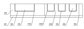
图1是本发明实现高性能金属-氧化物-金属的制造方法的在衬底上淀积形成刻蚀阻挡层和第一介电层后的示意图,请参见图1,步骤a:在以衬底上依次淀积一刻蚀阻挡层101和一第一介电层201;由于第一介电层201在后续工艺中将作为金属互连线区域,金属互联线区域需要采用低介电常数材料,故淀积第一介电层201采用的是低介电常数的材料。
Fig. 1 is a schematic diagram after depositing and forming an etch barrier layer and a first dielectric layer on the substrate of the present invention to realize the manufacturing method of high-performance metal-oxide-metal, please refer to Fig. 1, step a: on the substrate An
本发明中形成所述第一介电层201采用的材料可以从USG,FSG,BD,BDII等中选取。
The material used to form the first
本发明中的所述第一介电层201的厚度范围控制在1000~10000A之间。
The thickness range of the first
图2是本发明实现高性能金属-氧化物-金属的制造方法的形成金属-氧化物-金属区域图形后的示意图,请参见图2,步骤b:在第一介电层201上旋涂光刻胶,光刻形成金属-氧化物-金属区域的图形,使得后续工艺中可以通过刻蚀形成金属-氧化物-金属沟槽2021。
Fig. 2 is a schematic diagram of the present invention to realize a high-performance metal-oxide-metal manufacturing method after forming a metal-oxide-metal region pattern, please refer to Fig. 2, step b: spin-coat light on the first
图3是本发明实现高性能金属-氧化物-金属的制造方法的形成金属-氧化物-金属区域沟槽后的示意图,请参见图3,步骤c:刻蚀形成金属-氧化物-金属区域沟槽,使所述金属-氧化物-金属区域沟槽止于所述刻蚀阻挡层101,并去除光刻胶,为后续的第二介电层202填充做好准备;
Figure 3 is a schematic diagram of the present invention to realize the high-performance metal-oxide-metal manufacturing method after forming a metal-oxide-metal region trench, please refer to Figure 3, step c: etching to form a metal-oxide-metal region A trench, so that the trench in the metal-oxide-metal region stops at the
图4是本发明实现高性能金属-氧化物-金属的制造方法的淀积形成第二介电层后的示意图,请参见图4,步骤d:在第一介电层201上淀积第二介电层202,使所述第二介电层202填满所述金属-氧化物-金属区域沟槽,由于金属-氧化物-金属区域需填充高介电常数的材料以实现其高电容,故淀积第一介电层201与淀积第二介电层202采用的材料的介电常数不同,淀积第二介电层202采用的是高介电常数的材料
Fig. 4 is a schematic diagram of the present invention to realize the deposition of the second dielectric layer after the deposition of the high-performance metal-oxide-metal manufacturing method, please refer to Fig. 4, step d: deposit the second dielectric layer on the first
本发明中形成所述第二介电层202采用的材料从USG,FSG,BD,BD1,BDII中选取。
The material used to form the second
本发明中的所述第二介电层202的厚度范围控制在1000~10000A之间。
In the present invention, the thickness range of the second
图5是本发明实现高性能金属-氧化物-金属的制造方法的化学机械研磨后的示意图,请参见图5,步骤e:进行化学机械研磨平坦化,保留金属-氧化物-金属区域沟槽内的第二介电层202,将其与部分的第二介电层202清除,金属-氧化物-金属区域沟槽内的第二介电层202上表面与第一介电层201的上表面在同一水平面上;
Figure 5 is a schematic diagram of the present invention to realize the high-performance metal-oxide-metal manufacturing method after chemical mechanical polishing, please refer to Figure 5, step e: perform chemical mechanical polishing to planarize, and retain the metal-oxide-metal area groove The
图6是本发明实现高性能金属-氧化物-金属的制造方法的形成金属互连线沟槽和金属-氧化物-金属沟槽后的示意图,请参见图6,步骤f:通过光刻和刻蚀在第一介电层201上形成金属互连线沟槽2011,并同时在第二介电层202上形成金属-氧化物-金属沟槽2021,通过该工艺步骤实现了金属互联线沟槽置于低介电层、金属-氧化物-金属沟槽2021置于高介电层,从而可以在后续工艺中实现金属-氧化物-金属的高性能;
Figure 6 is a schematic diagram of the present invention to realize the high-performance metal-oxide-metal manufacturing method after forming metal interconnection trenches and metal-oxide-metal trenches, please refer to Figure 6, step f: through photolithography and Etching forms
图7是本发明实现高性能金属-氧化物-金属的制造方法的所有工艺完成后的结构示意图,请参见图7,步骤g:在金属互联线沟槽以及金属-氧化物-金属沟槽2021内同时进行铜扩散阻挡层301的淀积,之后进行电镀铜401工艺和化学机械研磨,实现了在同一层薄膜(第一介电层201与第二介电层202的上表面在同一高度,且第二介电层202填充于在第一介电层201上开设的沟槽内,故可以将第一介电层201与第二介电层202看做同一层薄膜)既有高介电常数材料,又有低介电常数材料,低介电常数材料区域做传统的金属互连,而高介电常数材料做金属-氧化物-金属电容,从而可以实现金属-氧化物-金属电容的高电容。
Fig. 7 is a schematic structural diagram of all the processes of the high-performance metal-oxide-metal manufacturing method of the present invention after completion, please refer to Fig. 7, step g: in the metal interconnection trench and the metal-oxide-
实施例(二) Example (2)
在实施例一的基础上,本发明可将金属互联线部分与金属-氧化物-金属部分的加工顺序互换,既首先完成高介电常数层的淀积,之后刻蚀形成金属互连线沟槽,再进行低介电常数层的淀积,其具体技术原理与实施例一相似,故实施例二的技术原理可参见实施例一中的相应技术原理。 On the basis of Embodiment 1, the present invention can exchange the processing sequence of the metal interconnection part and the metal-oxide-metal part, that is, the deposition of the high dielectric constant layer is completed first, and then the metal interconnection is formed by etching trench, and then deposit a low dielectric constant layer. The specific technical principle is similar to that of Embodiment 1, so the technical principle of Embodiment 2 can refer to the corresponding technical principle in Embodiment 1.
一种实现高性能金属-氧化物-金属的制造方法,其中, A method of fabricating a high-performance metal-oxide-metal, wherein,
步骤a:在以衬底上依次淀积一刻蚀阻挡层和一第一介电层; Step a: sequentially depositing an etch stop layer and a first dielectric layer on the substrate;
本实施例中淀积第一介电层采用的是高介电常数的材料,其中,形成所述第一介电层采用的材料可以从USG,FSG,BD,BD1,BDII等中选取。 In this embodiment, a material with a high dielectric constant is used to deposit the first dielectric layer, wherein the material used to form the first dielectric layer can be selected from USG, FSG, BD, BD1, BDII, and the like.
进一步的,所述第一介电层的厚度范围控制在1000~10000A之间较优。 Further, the thickness range of the first dielectric layer is preferably controlled between 1000-10000 Å.
步骤b:在第一介电层上旋涂光刻胶,光刻形成金属互连线区域的图形; Step b: Spin-coat photoresist on the first dielectric layer, and form a pattern of the metal interconnection line region by photolithography;
步骤c:刻蚀形成金属互连线区域沟槽,使所述金属互连线区域沟槽止于所述刻蚀阻挡层,并去除光刻胶; Step c: forming grooves in the metal interconnection area by etching, so that the grooves in the metal interconnection area stop at the etching barrier layer, and remove the photoresist;
步骤d:在第一介电层上淀积第二介电层,使所述第二介电层填满所述金属互连线区域沟槽; Step d: Depositing a second dielectric layer on the first dielectric layer, so that the second dielectric layer fills the grooves in the metal interconnection area;
本实施例中的淀积第一介电层与淀积第二介电层采用的材料的介电常数不同,其中,淀积第二介电层采用的是低介电常数的材料,形成所述第二介电层可以采用的材料从USG,FSG,BD,BDII等中选取。 In this embodiment, the dielectric constants of the materials used to deposit the first dielectric layer are different from those used to deposit the second dielectric layer, wherein the materials used to deposit the second dielectric layer are materials with low dielectric constants, forming the The material that can be used for the second dielectric layer is selected from USG, FSG, BD, BDII and the like.
较优的,本实施例中所述第二介电层的厚度范围控制在1000~10000A之间。 Preferably, the thickness range of the second dielectric layer in this embodiment is controlled between 1000-10000 Å.
步骤e:进行化学机械研磨平坦化,保留金属互连线沟区域槽内的第二介电层,将其与部分的第二介电层清除; Step e: Carrying out chemical mechanical polishing and planarization, retaining the second dielectric layer in the metal interconnection trench area, and removing it and part of the second dielectric layer;
步骤f:通过光刻和刻蚀在第一介电层上形成金属-氧化物-金属沟槽,并同时在第二介电层上形成金属互连线沟槽; Step f: forming metal-oxide-metal trenches on the first dielectric layer by photolithography and etching, and simultaneously forming metal interconnection trenches on the second dielectric layer;
步骤g:在金属互联线沟槽以及金属-氧化物-金属沟槽内同时进行铜扩散阻挡层的淀积,之后进行电镀铜工艺和化学机械研磨。 Step g: Depositing a copper diffusion barrier layer simultaneously in the metal interconnection trench and the metal-oxide-metal trench, followed by copper electroplating and chemical mechanical polishing.
综上所述,由于采用了上述技术方案,本发明实现高性能金属-氧化物-金属的制造方法解决了现有技术中金属-氧化物-金属区域与金属互联线区域均填充低K材料造成的金属-氧化物-金属区域无法实现高电容的问题,利用对第一介电层薄膜进行选择性的光刻蚀刻来定义金属-氧化物-金属(mental-oxide-mental,简称MOM)区域,在MOM区域填充高介电常数(高k)薄膜,来实现高性能MOM电容。通过这种方法,实现了在同一薄膜层既有高k材料又有低k材料。传统互连的区域为低k材料,高k材料区域做MOM,可以实现高电容,减少芯片使用面积,提高点穴性能。 In summary, due to the adoption of the above technical solution, the present invention realizes the high-performance metal-oxide-metal manufacturing method to solve the problem caused by filling the low-K material in the metal-oxide-metal region and the metal interconnection region in the prior art. The metal-oxide-metal region cannot achieve high capacitance. Selective photolithographic etching of the first dielectric layer film is used to define the metal-oxide-metal (mental-oxide-mental, MOM) region. High-permittivity (high-k) films are filled in the MOM region to achieve high-performance MOM capacitance. In this way, both high-k material and low-k material are realized in the same film layer. The area of traditional interconnection is made of low-k material, and the area of high-k material is made of MOM, which can achieve high capacitance, reduce the area used by the chip, and improve the hole performance.
以上对本发明的具体实施例进行了详细描述,但其只是作为范例,本发明并不限制于以上描述的具体实施例。对于本领域技术人员而言,任何对本发明进行的等同修改和替代也都在本发明的范畴之中。因此,在不脱离本发明的精神和范围下所作的均等变换和修改,都应涵盖在本发明的范围内。 The specific embodiments of the present invention have been described in detail above, but they are only examples, and the present invention is not limited to the specific embodiments described above. For those skilled in the art, any equivalent modifications and substitutions to the present invention are also within the scope of the present invention. Therefore, equivalent changes and modifications made without departing from the spirit and scope of the present invention shall fall within the scope of the present invention.
Claims (14)
Priority Applications (2)
| Application Number | Priority Date | Filing Date | Title |
|---|---|---|---|
| CN2011101638552A CN102427054A (en) | 2011-06-17 | 2011-06-17 | Manufacturing method for realizing high-performance metal-oxide-metal |
| US13/339,593 US8507355B2 (en) | 2011-06-17 | 2011-12-29 | Manufacturing method of a high performance metal-oxide-metal |
Applications Claiming Priority (1)
| Application Number | Priority Date | Filing Date | Title |
|---|---|---|---|
| CN2011101638552A CN102427054A (en) | 2011-06-17 | 2011-06-17 | Manufacturing method for realizing high-performance metal-oxide-metal |
Publications (1)
| Publication Number | Publication Date |
|---|---|
| CN102427054A true CN102427054A (en) | 2012-04-25 |
Family
ID=45961019
Family Applications (1)
| Application Number | Title | Priority Date | Filing Date |
|---|---|---|---|
| CN2011101638552A Pending CN102427054A (en) | 2011-06-17 | 2011-06-17 | Manufacturing method for realizing high-performance metal-oxide-metal |
Country Status (2)
| Country | Link |
|---|---|
| US (1) | US8507355B2 (en) |
| CN (1) | CN102427054A (en) |
Cited By (8)
| Publication number | Priority date | Publication date | Assignee | Title |
|---|---|---|---|---|
| CN102446917A (en) * | 2011-11-15 | 2012-05-09 | 上海华力微电子有限公司 | Multilayer metal-silicon nitride-metal capacitor and manufacturing method thereof |
| CN102800568A (en) * | 2012-09-11 | 2012-11-28 | 上海华力微电子有限公司 | Method for improving mass optical memory (MOM) capacitance density |
| CN102903611A (en) * | 2012-09-19 | 2013-01-30 | 上海集成电路研发中心有限公司 | Metal-dielectric-metal capacitor and manufacturing method thereof |
| CN102903612A (en) * | 2012-09-19 | 2013-01-30 | 上海集成电路研发中心有限公司 | Manufacture method of metal-oxide-metal capacitor |
| CN102931051A (en) * | 2012-10-09 | 2013-02-13 | 上海华力微电子有限公司 | Method for increasing MOM (Metal-Oxide-Metal) capacitance density |
| CN103531525A (en) * | 2012-07-02 | 2014-01-22 | 中芯国际集成电路制造(上海)有限公司 | Metal interconnection structure and manufacturing method thereof |
| CN105870051A (en) * | 2015-01-20 | 2016-08-17 | 中芯国际集成电路制造(上海)有限公司 | Semiconductor structure manufacturing method |
| CN112635438A (en) * | 2019-09-24 | 2021-04-09 | 中芯国际集成电路制造(上海)有限公司 | Semiconductor structure and forming method thereof |
Families Citing this family (2)
| Publication number | Priority date | Publication date | Assignee | Title |
|---|---|---|---|---|
| CN102916024B (en) | 2012-10-08 | 2015-12-02 | 上海华力微电子有限公司 | A kind of method forming dual-depth isolated groove |
| CN112247825B (en) * | 2020-09-04 | 2021-09-28 | 北京烁科精微电子装备有限公司 | Chip grinding method |
Citations (3)
| Publication number | Priority date | Publication date | Assignee | Title |
|---|---|---|---|---|
| US6777320B1 (en) * | 1998-11-13 | 2004-08-17 | Intel Corporation | In-plane on-chip decoupling capacitors and method for making same |
| US20060207965A1 (en) * | 2002-07-05 | 2006-09-21 | Chartered Semiconductor Manufacturing Ltd. | Method to form both high and low-k materials over the same dielectric region, and their application in mixed mode circuits |
| KR20100137125A (en) * | 2009-06-22 | 2010-12-30 | 주식회사 동부하이텍 | MOM capacitors and methods |
-
2011
- 2011-06-17 CN CN2011101638552A patent/CN102427054A/en active Pending
- 2011-12-29 US US13/339,593 patent/US8507355B2/en active Active
Patent Citations (3)
| Publication number | Priority date | Publication date | Assignee | Title |
|---|---|---|---|---|
| US6777320B1 (en) * | 1998-11-13 | 2004-08-17 | Intel Corporation | In-plane on-chip decoupling capacitors and method for making same |
| US20060207965A1 (en) * | 2002-07-05 | 2006-09-21 | Chartered Semiconductor Manufacturing Ltd. | Method to form both high and low-k materials over the same dielectric region, and their application in mixed mode circuits |
| KR20100137125A (en) * | 2009-06-22 | 2010-12-30 | 주식회사 동부하이텍 | MOM capacitors and methods |
Cited By (14)
| Publication number | Priority date | Publication date | Assignee | Title |
|---|---|---|---|---|
| CN102446917B (en) * | 2011-11-15 | 2014-02-05 | 上海华力微电子有限公司 | Multilayer MOM capacitor and manufacturing method thereof |
| CN102446917A (en) * | 2011-11-15 | 2012-05-09 | 上海华力微电子有限公司 | Multilayer metal-silicon nitride-metal capacitor and manufacturing method thereof |
| CN103531525B (en) * | 2012-07-02 | 2016-01-06 | 中芯国际集成电路制造(上海)有限公司 | The manufacture method of metal interconnect structure |
| CN103531525A (en) * | 2012-07-02 | 2014-01-22 | 中芯国际集成电路制造(上海)有限公司 | Metal interconnection structure and manufacturing method thereof |
| CN102800568A (en) * | 2012-09-11 | 2012-11-28 | 上海华力微电子有限公司 | Method for improving mass optical memory (MOM) capacitance density |
| CN102800568B (en) * | 2012-09-11 | 2016-01-20 | 上海华力微电子有限公司 | Improve the method for MOM capacitor density |
| CN102903612A (en) * | 2012-09-19 | 2013-01-30 | 上海集成电路研发中心有限公司 | Manufacture method of metal-oxide-metal capacitor |
| CN102903611A (en) * | 2012-09-19 | 2013-01-30 | 上海集成电路研发中心有限公司 | Metal-dielectric-metal capacitor and manufacturing method thereof |
| CN102903611B (en) * | 2012-09-19 | 2018-06-22 | 上海集成电路研发中心有限公司 | A kind of Metal-dielectric-metcapacitor capacitor and its manufacturing method |
| CN102931051A (en) * | 2012-10-09 | 2013-02-13 | 上海华力微电子有限公司 | Method for increasing MOM (Metal-Oxide-Metal) capacitance density |
| CN102931051B (en) * | 2012-10-09 | 2016-02-03 | 上海华力微电子有限公司 | Improve the method for MOM capacitor density |
| CN105870051A (en) * | 2015-01-20 | 2016-08-17 | 中芯国际集成电路制造(上海)有限公司 | Semiconductor structure manufacturing method |
| CN105870051B (en) * | 2015-01-20 | 2019-01-11 | 中芯国际集成电路制造(上海)有限公司 | The production method of semiconductor structure |
| CN112635438A (en) * | 2019-09-24 | 2021-04-09 | 中芯国际集成电路制造(上海)有限公司 | Semiconductor structure and forming method thereof |
Also Published As
| Publication number | Publication date |
|---|---|
| US8507355B2 (en) | 2013-08-13 |
| US20120322256A1 (en) | 2012-12-20 |
Similar Documents
| Publication | Publication Date | Title |
|---|---|---|
| CN102427054A (en) | Manufacturing method for realizing high-performance metal-oxide-metal | |
| CN102222643B (en) | Method for redundant metal filling in integrated circuit manufacturing process and semiconductor device | |
| US20130260552A1 (en) | Reverse Damascene Process | |
| CN102569032B (en) | Method for manufacturing inductance element by overlapping multiple layers of metalized thin films | |
| CN109427656B (en) | Semiconductor device and method for manufacturing the same | |
| CN107731739A (en) | The forming method of semiconductor structure | |
| US10276377B2 (en) | Method for patterning interconnects | |
| CN101414606A (en) | Stack capacitor in semiconductor device and method for fabricating the same | |
| TWI725062B (en) | Structure and method of fabricating three-dimensional (3d) metal-insulator-metal (mim) capacitor and resistor in semi-additive plating metal wiring | |
| CN102610563A (en) | Method for preparing copper dual damascene structure | |
| TWI668728B (en) | Dummy gate used as interconnection and method of making the same | |
| CN113206196A (en) | Three-dimensional MIM capacitor based on through silicon via technology and preparation method thereof | |
| JP2004172620A (en) | Integrated circuit with air gaps and its manufacturing method | |
| CN108231739A (en) | The air gap of isolating metal feature | |
| CN102738076B (en) | Through hole propriety copper interconnection manufacturing method | |
| KR100871768B1 (en) | Semiconductor element and COA / COA manufacturing method | |
| US9177929B2 (en) | Techniques for fabricating fine-pitch micro-bumps | |
| CN104112702B (en) | The method reducing ultra-low-k dielectric layer damage in semiconductor fabrication | |
| CN108511473B (en) | Interconnection process for metal layers between wafers | |
| CN103531528B (en) | Method for manufacturing dual damascene structure | |
| CN102082118A (en) | Method for producing dual-damascene structure | |
| CN108091640B (en) | Integrated capacitor and method of forming the same | |
| CN103325729A (en) | Copper interconnection structure manufacturing method | |
| CN102592993A (en) | Method for improving uniformity of chemical mechanical planarization process of back gate engineering metal plug | |
| CN1697124A (en) | How to make a capacitor |
Legal Events
| Date | Code | Title | Description |
|---|---|---|---|
| C06 | Publication | ||
| PB01 | Publication | ||
| C10 | Entry into substantive examination | ||
| SE01 | Entry into force of request for substantive examination | ||
| C02 | Deemed withdrawal of patent application after publication (patent law 2001) | ||
| WD01 | Invention patent application deemed withdrawn after publication |
Application publication date: 20120425 |