CN102414820A - Methods, devices, and systems relating to memory cells having a floating body - Google Patents
Methods, devices, and systems relating to memory cells having a floating body Download PDFInfo
- Publication number
- CN102414820A CN102414820A CN2010800197787A CN201080019778A CN102414820A CN 102414820 A CN102414820 A CN 102414820A CN 2010800197787 A CN2010800197787 A CN 2010800197787A CN 201080019778 A CN201080019778 A CN 201080019778A CN 102414820 A CN102414820 A CN 102414820A
- Authority
- CN
- China
- Prior art keywords
- silicon
- gate
- region
- recess
- memory cell
- Prior art date
- Legal status (The legal status is an assumption and is not a legal conclusion. Google has not performed a legal analysis and makes no representation as to the accuracy of the status listed.)
- Granted
Links
Images


Classifications
-
- H—ELECTRICITY
- H10—SEMICONDUCTOR DEVICES; ELECTRIC SOLID-STATE DEVICES NOT OTHERWISE PROVIDED FOR
- H10B—ELECTRONIC MEMORY DEVICES
- H10B12/00—Dynamic random access memory [DRAM] devices
- H10B12/20—DRAM devices comprising floating-body transistors, e.g. floating-body cells
-
- H—ELECTRICITY
- H10—SEMICONDUCTOR DEVICES; ELECTRIC SOLID-STATE DEVICES NOT OTHERWISE PROVIDED FOR
- H10B—ELECTRONIC MEMORY DEVICES
- H10B12/00—Dynamic random access memory [DRAM] devices
-
- H—ELECTRICITY
- H10—SEMICONDUCTOR DEVICES; ELECTRIC SOLID-STATE DEVICES NOT OTHERWISE PROVIDED FOR
- H10D—INORGANIC ELECTRIC SEMICONDUCTOR DEVICES
- H10D30/00—Field-effect transistors [FET]
- H10D30/60—Insulated-gate field-effect transistors [IGFET]
- H10D30/711—Insulated-gate field-effect transistors [IGFET] having floating bodies
Landscapes
- Semiconductor Memories (AREA)
- Non-Volatile Memory (AREA)
Abstract
Description
相关申请案交叉参考Related Application Cross Reference
本申请案主张2009年4月7日提出申请的序列号为12/419,658的美国专利申请案“关于具有浮动主体的存储器单元的方法、装置及系统(Methods,Devices,and SystemsRelating to Memory Cell Having a Floating Body)”的申请日期的权益。This application asserts U.S. Patent Application Serial No. 12/419,658 filed April 7, 2009 "Methods, Devices, and Systems Relating to Memory Cell Having a Floating Body Floating Body)" filing date.
技术领域 technical field
一般来说,本发明的实施例涉及存储器单元。更特定来说,本发明的实施例涉及具有浮动主体的存储器单元、利用所述存储器单元的装置及系统以及形成所述存储器单元的方法及操作所述存储器单元的方法。In general, embodiments of the invention relate to memory cells. More particularly, embodiments of the invention relate to memory cells having floating bodies, devices and systems utilizing the memory cells, and methods of forming and operating the memory cells.
背景技术 Background technique
常规存储器(举例来说,DRAM)可包含一个晶体管及一个电容器。然而,由于所述电容器的存在(且特定来说是所述电容器的大小),常规存储器的可缩放性存在限制。因此,已开发包含一个晶体管(1T)且不包含电容器作为存储器单元、称为“无电容器”存储器的存储器。无电容器存储器单元可包含浮动主体(即,电浮动的主体)。Conventional memory, such as DRAM, may include one transistor and one capacitor. However, there is a limit to the scalability of conventional memory due to the presence of the capacitor (and in particular the size of the capacitor). Accordingly, memories have been developed that contain one transistor (IT) and no capacitor as a memory cell, known as "capacitorless" memories. A capacitorless memory cell may include a floating body (ie, a body that floats electrically).
一般来说,常规无电容器存储器单元利用绝缘体上硅(SOI)晶片且识别通过在浮动主体中积累多数载流子(空穴或电子)或通过从所述浮动主体发射多数载流子来控制浮动主体电压的数据。如所属领域的技术人员所理解,可通过致使多数载流子积累且保持于浮动主体中而将逻辑“1”写入到且存储于存储器单元中。如此,当在所述浮动主体中积累多数载流子时,此状态通常称为数据“1”状态。可通过从所述浮动主体移除多数载流子来擦除逻辑“1”(即,写入逻辑“0”)。如此,当从所述浮动主体排空多数载流子时,此状态通常称为数据“0”状态。而且如所属领域的技术人员所理解,晶体管浮动主体中的所存储电荷影响存储器单元晶体管的阈值电压(VT)。较低阈值电压(VT)增加穿过所述存储器单元晶体管的电流,且较高阈值电压(VT)减小穿过所述晶体管的电流。穿过所述存储器单元晶体管的电流用于确定所述存储器单元的状态。In general, conventional capacitorless memory cells utilize silicon-on-insulator (SOI) wafers and recognize that the floating body is controlled by accumulating majority carriers (holes or electrons) in the floating body or by emitting majority carriers from the floating body. Body voltage data. As understood by those skilled in the art, a logic "1" can be written to and stored in a memory cell by causing majority carriers to accumulate and remain in the floating body. As such, when majority carriers accumulate in the floating body, this state is often referred to as a data "1" state. A logical "1" can be erased (ie, written to a logical "0") by removing majority carriers from the floating body. As such, when majority carriers are emptied from the floating body, this state is often referred to as a data "0" state. Also as understood by those skilled in the art, the stored charge in the floating body of a transistor affects the threshold voltage ( VT ) of the memory cell transistor. A lower threshold voltage ( VT ) increases the current through the memory cell transistor, and a higher threshold voltage ( VT ) decreases the current through the transistor. The current through the memory cell transistor is used to determine the state of the memory cell.
图1图解说明常规浮动主体存储器单元10的实例。存储器单元10包含具有栅极区16、源极区18及漏极区20的晶体管12。源极区18及漏极区20形成于硅层26中,其中浮动主体区24界定于所述源极区与所述漏极区之间。此外,浮动主体区24安置于上覆于衬底30上的绝缘层28上。存储器单元10还包含区38,所述区包括与浮动主体区24相比是高度正掺杂,但相比源极区18或漏极区20是正掺杂程度较轻的硅。区38借助穿过绝缘层28、硅层26及绝缘层32的导电线41连接到触点40。通过在绝缘层28具有400纳米的厚度时将负电压(通常在-20V左右)施加到区38,可在浮动主体区24中形成中性区。因此,可在浮动主体区24内产生且存储电荷。FIG. 1 illustrates an example of a conventional floating
如上文所图解说明,常规浮动主体存储器单元将电荷存储于邻近于漏极区及源极区的浮动主体内,且因此,所述所存储电荷具有在操作期间从所述浮动主体中泄漏的趋向。此在较高温度下的操作期间尤其成问题。另外,常规浮动主体存储器单元在保持、读取及写入操作期间由于电荷重组之后即刻从所述浮动主体丢失电荷而遭受不良数据保持。此外,由于常规浮动主体存储器单元可具有未被配置为保持大量电荷的小浮动主体,因此任何电荷丢失均可导致波动或弱化信号。As illustrated above, conventional floating body memory cells store charge within the floating body adjacent to the drain and source regions, and thus, the stored charge has a tendency to leak from the floating body during operation. . This is especially problematic during operation at higher temperatures. Additionally, conventional floating body memory cells suffer from poor data retention during hold, read, and write operations due to loss of charge from the floating body immediately after charge recombination. Furthermore, since conventional floating body memory cells can have small floating bodies that are not configured to hold large amounts of charge, any loss of charge can lead to fluctuating or weakened signals.
需要用于增强浮动主体存储器单元的功能性的方法、装置及系统。具体来说,需要用于通过增加存储器单元的浮动主体的大小且增加浮动主体存储器单元的数据保持来增强存储器单元的功能性的方法、装置及系统。Methods, devices, and systems for enhancing the functionality of floating body memory cells are needed. In particular, there is a need for methods, devices, and systems for enhancing the functionality of memory cells by increasing the size of their floating bodies and increasing the data retention of the floating body memory cells.
发明内容 Contents of the invention
下文描述本发明的各种实施例,且所述实施例针对存储器单元、形成存储器单元的方法、包含具有多个存储器单元的存储器阵列的存储器装置、操作存储器阵列的方法及包含至少一个存储器装置(其包含具有多个存储器单元的存储器阵列)的电子系统的实施例。在至少一个实施例中,存储器单元可包括包含源极、漏极及定位于所述源极与所述漏极之间的栅极的晶体管。此外,所述存储器单元可包含具有邻近所述源极及所述漏极中的每一者而定位的第一部分以及远离所述源极及所述漏极中的每一者的第二部分的硅。所述硅可包含将所述第一部分耦合到所述第二部分的通路。此外,所述存储器单元可包含凹入到所述硅中且定位于所述第一部分与所述第二部分之间的偏置栅极。所述偏置栅极可经配置以用于可操作地耦合到偏置电压。所述存储器单元还可包含至少部分地环绕所述偏置栅极的电介质材料及邻近于所述硅且包括另一电介质材料的隔离区。所述第二部分可定位于所述隔离区与所述偏置栅极之间。Various embodiments of the invention are described below and are directed to memory cells, methods of forming memory cells, memory devices including memory arrays having a plurality of memory cells, methods of operating memory arrays, and memory devices including at least one ( It includes an embodiment of an electronic system having a memory array having a plurality of memory cells. In at least one embodiment, a memory cell can include a transistor including a source, a drain, and a gate positioned between the source and the drain. Furthermore, the memory cell can include a memory cell having a first portion positioned adjacent to each of the source and the drain and a second portion remote from each of the source and the drain silicon. The silicon can include vias coupling the first portion to the second portion. Furthermore, the memory cell can include an offset gate recessed into the silicon and positioned between the first portion and the second portion. The bias gate can be configured for operably coupling to a bias voltage. The memory cell may also include a dielectric material at least partially surrounding the bias gate and an isolation region adjacent to the silicon and including another dielectric material. The second portion can be positioned between the isolation region and the bias gate.
在至少一个其它实施例中,存储器单元可包括晶体管,所述晶体管具有各自形成于硅中的漏极及源极以及定位于所述漏极与所述源极之间的栅极。所述存储器单元还可包含凹入到所述硅中且定位于隔离区与所述晶体管之间的偏置栅极。所述偏置栅极可经配置以可操作地耦合到偏置电压。另外,所述存储器单元可包含位于所述硅内且具有邻近所述源极及所述漏极的第一部分及耦合到所述第一部分的第二部分的浮动主体。所述第一部分可从所述偏置栅极垂直偏移且所述偏置栅极可邻近所述第二部分而形成。In at least one other embodiment, a memory cell can include a transistor having a drain and a source each formed in silicon and a gate positioned between the drain and the source. The memory cell may also include a bias gate recessed into the silicon and positioned between an isolation region and the transistor. The bias gate can be configured to be operatively coupled to a bias voltage. Additionally, the memory cell can include a floating body within the silicon and having a first portion adjacent to the source and drain and a second portion coupled to the first portion. The first portion can be vertically offset from the offset gate and the offset gate can be formed adjacent to the second portion.
本发明的其它实施例可包含形成存储器单元的方法。一种方法可包括形成具有形成于硅中的源极及漏极以及定位于所述源极与所述漏极之间的栅极的晶体管。另外,所述方法可包含形成进入到所述硅中但不穿过所述硅且定位于所述晶体管与穿过所述硅形成的隔离区之间的凹部。此外,所述凹部可远离所述隔离区。所述方法还可包含沿着所述凹部的表面且邻近所述硅形成电介质。所述方法还可包括至少部分地在所述凹部内形成导电材料。Other embodiments of the invention may include methods of forming memory cells. A method may include forming a transistor having a source and a drain formed in silicon and a gate positioned between the source and the drain. Additionally, the method may include forming a recess into but not through the silicon and positioned between the transistor and an isolation region formed through the silicon. Furthermore, the recess may be remote from the isolation region. The method can also include forming a dielectric along a surface of the recess and adjacent to the silicon. The method may also include forming a conductive material at least partially within the recess.
一个或一个以上其它实施例可包括操作包含多个存储器单元的存储器阵列的方法。一种方法可包含将偏置电压施加到邻近所述多个存储器单元中的每一存储器单元的电荷存储区的偏置栅极。所述方法还可包含通过以下方式中的一者对包括晶体管的存储器单元执行操作:将电荷编程到所述存储器单元的浮动主体内的相关联电荷存储区,及从所述相关联电荷存储区读取电荷。所述相关联电荷存储区可邻近隔离区而定位、从所述晶体管垂直偏移,且耦合到所述浮动主体内的另一区。另外,所述另一区可邻近所述晶体管。One or more other embodiments may include methods of operating a memory array including a plurality of memory cells. A method may include applying a bias voltage to a bias gate adjacent to a charge storage region of each memory cell of the plurality of memory cells. The method may also include performing an operation on a memory cell comprising a transistor by one of programming charge into an associated charge storage region within a floating body of the memory cell, and from the associated charge storage region Read charge. The associated charge storage region may be positioned adjacent to an isolation region, vertically offset from the transistor, and coupled to another region within the floating body. Additionally, the another region may be adjacent to the transistor.
在又一些实施例中,本发明包含包括存储器阵列的存储器装置,所述存储器阵列包含根据先前所述的实施例中的一者或一者以上的多个存储器单元。本发明的再一些实施例包含电子系统。此些系统的一个或一个以上实施例可包括至少一个处理器及包含多个根据先前所述的实施例中的一者或一者以上的存储器单元的至少一个存储器装置。In yet other embodiments, the present invention includes a memory device comprising a memory array comprising a plurality of memory cells according to one or more of the previously described embodiments. Still other embodiments of the invention include electronic systems. One or more embodiments of such systems may include at least one processor and at least one memory device including a plurality of memory units according to one or more of the previously described embodiments.
附图说明 Description of drawings
图1图解说明常规浮动主体存储器单元;Figure 1 illustrates a conventional floating body memory cell;
图2是根据本发明的实施例的存储器单元的横截面图;2 is a cross-sectional view of a memory cell according to an embodiment of the invention;
图3是根据本发明的实施例的包含多个存储器单元的存储器阵列的一部分的横截面图;3 is a cross-sectional view of a portion of a memory array including a plurality of memory cells according to an embodiment of the invention;
图4A及图4B分别图解说明根据本发明的实施例的结构的形成的平面图及横截面图;4A and 4B are plan and cross-sectional views, respectively, illustrating the formation of structures according to embodiments of the invention;
图5A是根据本发明的实施例的图4A结构的进一步形成的平面图;5A is a plan view of a further development of the structure of FIG. 4A in accordance with an embodiment of the present invention;
图5B是根据本发明的实施例的图4B结构的进一步形成的横截面图;5B is a further developed cross-sectional view of the structure of FIG. 4B in accordance with an embodiment of the invention;
图6A是根据本发明的实施例的图5A结构的进一步形成的平面图;Figure 6A is a plan view of a further development of the structure of Figure 5A in accordance with an embodiment of the present invention;
图6B是根据本发明的实施例的图5B结构的进一步形成的横截面图;6B is a further developed cross-sectional view of the structure of FIG. 5B in accordance with an embodiment of the present invention;
图7A是根据本发明的实施例的图6A结构的进一步形成的平面图;7A is a plan view of a further development of the structure of FIG. 6A in accordance with an embodiment of the present invention;
图7B是根据本发明的实施例的图6B结构的进一步形成的横截面图;7B is a further developed cross-sectional view of the structure of FIG. 6B in accordance with an embodiment of the invention;
图8A是根据本发明的实施例的图7A结构的进一步形成的平面图;Figure 8A is a plan view of a further development of the structure of Figure 7A in accordance with an embodiment of the present invention;
图8B是根据本发明的实施例的图7B结构的进一步形成的横截面图;8B is a further developed cross-sectional view of the structure of FIG. 7B in accordance with an embodiment of the invention;
图9A是根据本发明的实施例的图8A结构的进一步形成的平面图;9A is a plan view of a further development of the structure of FIG. 8A in accordance with an embodiment of the present invention;
图9B是根据本发明的实施例的图8B结构的进一步形成的横截面图;9B is a further developed cross-sectional view of the structure of FIG. 8B in accordance with an embodiment of the present invention;
图10A是根据本发明的实施例的图9A结构的进一步形成的平面图;Figure 10A is a further developed plan view of the structure of Figure 9A in accordance with an embodiment of the present invention;
图10B是根据本发明的实施例的图9B结构的进一步形成的横截面图;Figure 10B is a further developed cross-sectional view of the structure of Figure 9B in accordance with an embodiment of the present invention;
图11A是根据本发明的另一实施例的结构的形成的平面图;Figure 11A is a plan view of the formation of a structure according to another embodiment of the invention;
图11B是根据本发明的实施例的图11A中所图解说明的结构的形成的横截面图;11B is a cross-sectional view of the formation of the structure illustrated in FIG. 11A according to an embodiment of the invention;
图11C是图解说明于图11A中且相对于图11A旋转90度的结构的另一平面图;Figure 11C is another plan view of the structure illustrated in Figure 11A and rotated 90 degrees relative to Figure 11A;
图11D是图解说明于图11B中且相对于图11B旋转90度的结构的另一横截面图;11D is another cross-sectional view of the structure illustrated in FIG. 11B and rotated 90 degrees relative to FIG. 11B;
图12A及图12B分别图解说明根据本发明的另一实施例的又一结构的形成的平面图及横截面图;12A and 12B are plan and cross-sectional views, respectively, illustrating the formation of yet another structure according to another embodiment of the invention;
图13是根据本发明的实施例的存储器单元的电路图;Figure 13 is a circuit diagram of a memory cell according to an embodiment of the present invention;
图14是根据本发明的实施例的电子系统的框图;且14 is a block diagram of an electronic system according to an embodiment of the invention; and
图15是根据本发明的实施例的包含并入有先前实施例中的一者或一者以上的存储器单元的集成电路裸片的半导体晶片的图示。15 is an illustration of a semiconductor wafer including an integrated circuit die incorporating one or more memory cells from previous embodiments, according to an embodiment of the invention.
具体实施方式 Detailed ways
在以下实施方式中,参考形成本发明的一部分的附图,且附图中以图解说明的方式展示其中可实践本发明的特定实施例。足够详细地描述这些实施例以使得所属领域的技术人员能够实践本发明,且应理解,可利用其它实施例并可在本发明的范围内做出结构、逻辑及电改变。In the following detailed description, reference is made to the accompanying drawings which form a part hereof, and in which is shown by way of illustration specific embodiments in which the invention may be practiced. These embodiments are described in sufficient detail to enable those skilled in the art to practice the invention, and it is to be understood that other embodiments may be utilized and structural, logical, and electrical changes may be made within the scope of the invention.
在此说明中,可以框图形式展示功能,以便不会以不必要的细节使本发明模糊不清。此外,所示及所述的特定实施方案仅为实例且不应视为实施本发明的仅有方式,除非本文中另有规定。框界定及各种框之间的逻辑分割表示特定实施方案。所属领域的技术人员将易于明了,可通过众多其它分割方案来实践本发明的各种实施例。在大多数情况下,本发明的各种实施例中已省略关于时序考虑的细节等,其中此些细节对获得对本发明的各种实施例的完全理解并非必要的且在相关领域的技术人员的能力范围内。In this description, functionality may be shown in block diagram form in order not to obscure the invention in unnecessary detail. Furthermore, the particular implementations shown and described are examples only and should not be construed as the only ways to practice the invention unless otherwise specified herein. The block demarcations and logical divisions between the various blocks represent specific implementations. It will be readily apparent to those skilled in the art that various embodiments of the invention may be practiced with numerous other partitioning schemes. In most cases, details regarding timing considerations, etc., have been omitted from the various embodiments of the invention, where such details are not necessary to gain a complete understanding of the various embodiments of the invention and are within the purview of those skilled in the relevant art within ability.
以下说明中所用的术语“晶片”及“衬底”包含具有经暴露表面的任一结构,可在所述结构上或所述结构中形成与本发明的实施例相关的集成电路(IC)结构。非限制性地,术语衬底包含半导体晶片及其它块体半导体衬底。术语衬底还用于指代在处理期间的半导体结构,且可包含已制作于其上的其它层。晶片及衬底两者均包含经掺杂及未经掺杂的半导体、由基底半导体或绝缘体支撑的外延半导体层以及所属领域的技术人员已知的其它半导体结构。术语“导体”包含半导体,且术语“绝缘体”或“电介质”包含导电性不及本文中称为导体的材料的任一材料。The terms "wafer" and "substrate" as used in the following description include any structure having an exposed surface on or in which integrated circuit (IC) structures related to embodiments of the present invention may be formed . Without limitation, the term substrate includes semiconductor wafers and other bulk semiconductor substrates. The term substrate is also used to refer to a semiconductor structure during processing and may include other layers that have been fabricated thereon. Both wafers and substrates include doped and undoped semiconductors, epitaxial semiconductor layers supported by base semiconductors or insulators, and other semiconductor structures known to those skilled in the art. The term "conductor" includes semiconductors, and the terms "insulator" or "dielectric" include any material that is less conductive than the material referred to herein as a conductor.
大体参考以下说明及附图,图解说明本发明的各种方面以展示其结构及操作方法。以相似编号指示所图解说明实施例的共同元件。应理解,所呈现的图并非打算图解说明实际结构或方法的任一特定部分的实际视图,而仅是用来更清晰且更充分地描绘本发明的理想化表示。Referring generally to the following description and accompanying drawings, various aspects of the invention are illustrated to show its structure and method of operation. Common elements of the illustrated embodiments are designated with like numerals. It should be understood that the presented figures are not intended to illustrate actual views of any particular portion of the actual structure or method, but are merely idealized representations used to more clearly and fully depict the invention.
将首先参考图2及图3描述根据本发明的各种实施例的包含浮动主体的存储器单元及包含多个存储器单元的存储器阵列。接着将参考图4A到图10B来描述根据本发明的各种实施例的形成包含多个存储器单元的存储器阵列的方法。接着将参考图11A到图12B来描述根据本发明的其它实施例的包含多个存储器单元的存储器阵列。此后,接着将参考图13来描述根据本发明的实施例的存储器单元的各种操作。此外,参考图14及图15,将描述各自并入有先前实施例中的一者或一者以上的存储器阵列及存储器单元的电子系统及半导体晶片。A memory cell including a floating body and a memory array including a plurality of memory cells according to various embodiments of the present invention will first be described with reference to FIGS. 2 and 3 . Methods of forming a memory array including a plurality of memory cells according to various embodiments of the present invention will next be described with reference to FIGS. 4A to 10B . Next, memory arrays including a plurality of memory cells according to other embodiments of the present invention will be described with reference to FIGS. 11A to 12B . Thereafter, various operations of the memory cell according to the embodiment of the present invention will be described next with reference to FIG. 13 . Furthermore, with reference to FIGS. 14 and 15 , electronic systems and semiconductor wafers each incorporating the memory array and memory cells of one or more of the previous embodiments will be described.
应注意,虽然本发明的以下所述实施例包括一个或一个以上NMOS晶体管,但所属领域的技术人员已知的其它晶体管(例如,PMOS晶体管)可用于实施本发明的各种实施例。此外,虽然本发明的以下所述实施例是指“空穴产生”或充当多数载流子的“空穴”,但所属领域的技术人员将理解,在提供(举例来说)电子产生及充当多数载流子的电子的特定实施例中可反转各种电压及/或掺杂极性。It should be noted that while the below-described embodiments of the invention include one or more NMOS transistors, other transistors (eg, PMOS transistors) known to those skilled in the art may be used to implement various embodiments of the invention. Furthermore, although the embodiments of the invention described below refer to "hole generation" or "holes" acting as majority carriers, those skilled in the art will understand that in providing, for example, electron generation and serving as Various voltages and/or doping polarities can be reversed in certain embodiments of majority carrier electrons.
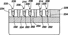
图2是根据本发明的各种实施例的包含浮动主体的存储器单元210的横截面图。如图2中所图解说明,存储器单元210包含具有有源栅极214、源极216及漏极218的晶体管212。另外,存储器单元210包含上覆于隐埋绝缘体222上的区234,所述区可包括硅。如所图解说明,有源栅极214定位于在区234中形成的第一凹部280内。晶体管212可形成于可上覆于衬底220上的隐埋绝缘体222上方。仅举例来说,且并非以限制方式,隐埋绝缘体222可包括隐埋氧化物(BOX)且衬底220可包括块体硅衬底。2 is a cross-sectional view of a
此外,存储器单元210包含定位于在区234内形成的第二凹部282内的偏置栅极236。仅举例来说,偏置栅极236可包括多晶硅或任一其它金属。另外,存储器单元210可包括沿着第一凹部280的邻近于区234的表面及沿着第二凹部282的邻近于区234的表面形成的电介质材料233。此外,电介质材料233可形成于区234在第二凹部282与浅沟槽隔离(STI)区228(其可包括电介质材料229)之间的一部分上方。存储器单元210还可包含上覆于浅沟槽隔离(STI)区228及形成于区234的一部分上方的电介质材料233中的每一者上的氮化硅238。此外,氮化硅238可上覆于第二凹部282内的偏置栅极236及第一凹部280内的有源栅极214中的每一者上。Additionally,
区234可包含邻近有源栅极214、漏极218及源极216的第一部分284。此外,区234可包含邻近偏置栅极236且远离有源栅极214、漏极218及源极216的第二部分286。下文中也可将第二部分286称为“电荷存储区”。此外,第一部分284可经由定位于偏置栅极236的底部端与区234的底部表面之间的通路288耦合到第二部分286。仅举例来说,且并非以限制方式,通路288可具有在(仅举例来说)大致20纳米到75纳米的范围中的高度P。第一部分284、通路288及第二部分286可共同界定存储器单元210的浮动主体。
存储器单元210还可包含上覆于氮化硅238上的氧化物区240。此外,可穿过氧化物区240形成共用源极线226且所述共用源极线可操作地耦合到源极216。存储器单元210还可包含数字线224,所述数字线上覆于氧化物区248上且延伸穿过形成于氧化物区248及氧化物区240中的每一者中的通道以可操作地耦合到漏极218。
如下文更充分地描述,在存储器单元210的预期操作期间,偏置栅极236可操作地耦合到偏置电压,且更具体来说,耦合到负偏置电压。因此,在操作期间,第二部分286连同沿着第二凹部282的外表面形成的电介质材料233、STI区228及偏置栅极236一起可共同地充当一电容器。因此,产生于浮动主体(即,第一部分284、通路288及第二部分286)内的空穴可被吸引到第二部分286且存储于第二部分286内。因此,在存储器单元210的操作期间,电荷可远离源极216及漏极218中的每一者存储,且因此,相对于常规浮动主体存储器单元可减小电荷重组的任何趋向。此外,经由通路288将第二部分286耦合到第一部分284可限制在存储器单元210的操作期间移动到第二部分286中或移动出第二部分286的电荷的数目。因此,与常规浮动主体存储器单元相比,可增强电荷保持。此外,如所配置,存储器单元210可包含与常规现有技术结构的浮动主体相比具有较大存储面积的浮动主体。因此,此可使得能够存储更多的电荷,且因此,使由于任一丢失电荷所致的信号波动最小化。因此,与常规结构相比,存储器单元210可提供增强的信号。另外,应注意,可增加区234的高度H且因此可增加电荷存储区286的面积以使得能够在电荷存储区286内存储较大量的电荷。As described more fully below,
图3是根据本发明的实施例的包含多个存储器单元210的存储器阵列200的一部分的横截面图。图2及图3中已使用相似编号来识别相似特征。3 is a cross-sectional view of a portion of a
参考图4A到图10B,现在将描述根据本发明的各种实施例形成包含多个存储器单元的存储器阵列的方法。在一个实施例中,如在图4A中所图解说明的平面图及图4B中所图解说明的横截面图中所描绘,可提供包含在衬底220上方的隐埋绝缘体222的结构。如上文所提及,隐埋绝缘体222可包括(举例来说)隐埋氧化物(BOX),且衬底220可包括(举例来说)块体硅衬底。此外,仅举例来说,隐埋绝缘体222可具有在大致100纳米到300纳米的范围中的垂直厚度。此外,所述结构可包含上覆于隐埋绝缘体222上的区234。如上文所提及,区234可包括硅且可具有在(仅举例来说)大致50纳米到200纳米的范围中的高度H。此外,所述结构可包含穿过区234形成的浅沟槽隔离(STI)区228。可使用反应性离子蚀刻(RIE)工艺或所属领域的技术人员已知的其它适合蚀刻工艺形成STI区228。可在每一STI区228内形成电介质材料229(例如,仅举例来说,二氧化硅(SiO2)、旋涂玻璃(SOG)或其它适合电介质材料)。接着可通过研磨工艺(例如,化学机械平面化(CMP))来对顶部电介质材料229进行平面化。此外,应注意,在于(STI)区228内形成电介质材料229之前,可氧化区234的邻近(STI)区228的侧壁以修补因形成STI区228所造成的任何损坏。Referring to FIGS. 4A-10B , methods of forming a memory array including a plurality of memory cells according to various embodiments of the present invention will now be described. In one embodiment, a structure including a buried
参考图5A中所图解说明的平面图及图5B中所图解说明的横截面图,可将第一凹部280及第二凹部282蚀刻到区234中。仅举例来说,可使用RIE工艺或所属领域的技术人员已知的任一其它蚀刻工艺将第一凹部280及第二凹部282蚀刻到区234中。仅举例来说,且并非以限制方式,可将第一凹部280及第二凹部282蚀刻到区234中达特定深度以便在区234的底部表面与第一凹部280及第二凹部282中的每一者的底部端之间留下大致20纳米到75纳米的区234。Referring to the plan view illustrated in FIG. 5A and the cross-sectional view illustrated in FIG. 5B , a
此外,可在区234的顶部表面上方且沿着第一凹部280及第二凹部282中的每一者的表面形成电介质233。举例来说,根据一个实施例,可通过选择性地氧化区234的顶部表面及区234的邻近每一第一凹部280及每一第二凹部282的表面来形成电介质233。根据另一实施例,可通过任一已知的适合沉积工艺形成电介质233。仅举例来说,与二氧化硅相比,电介质233可包括高K电介质材料。Furthermore, dielectric 233 may be formed over the top surface of
此后,如在图6A中所图解说明的平面图及图6B中所图解说明的横截面图中所描绘,可在每一第一凹部280内形成有源栅极214且可在每一第二凹部282内形成偏置栅极236。有源栅极214及偏置栅极336中的每一者可包括(举例来说)金属,例如氮化钛(TiN)、氮化钽(TaN)、其任一组合或任一其它金属。仅举例来说,且并非以限制方式,可通过任一已知金属硅化物沉积工艺或所属领域的技术人员已知的任一其它工艺来形成偏置栅极236及有源栅极214中的每一者。此后,可通过所属领域的技术人员已知的任一工艺蚀刻第一凹部280内的每一有源栅极214及第二凹部282内的每一偏置栅极236的一部分以形成凹陷235。可通过(仅举例来说)毯覆RIE工艺形成凹陷235。此外,仅举例来说,凹陷235可形成到区234的顶部表面下方大致20纳米到75纳米的深度。Thereafter, as depicted in the plan view illustrated in FIG. 6A and the cross-sectional view illustrated in FIG. 6B , an
随后,如在图7A中所图解说明的平面图及图7B中所图解说明的横截面图中所描绘,可通过所属领域的技术人员已知的任一工艺在区234内形成源极216及漏极218。此外,可通过任一已知工艺在区234及电介质材料229中的每一者上方形成可包括(举例来说)氮化硅的电介质238。还可在偏置栅极236及有源栅极214上方的每一凹陷235内形成电介质238。
此外,参考图8A中所图解说明的平面图及图8B中所图解说明的横截面图,使用任一已知工艺,可在电介质238上方形成氧化物区240。随后,如在图9A及图9B中所图解说明,可使用常规镶嵌工艺来形成延伸穿过氧化物区240及电介质238中的每一者且耦合到源极216的共用源极线226。接着可通过研磨工艺(例如,CMP工艺)对每一共用源极线226的顶部进行平面化。仅举例来说,共用源极线226可包括氮化钛(TiN)、氮化钽(TaN)、钨(W)、其任一组合或任一其它金属。此后,参考图10A中所图解说明的平面图及图10B中所图解说明的横截面图,使用任一已知工艺,可在氧化物区240及共用源极线226上方形成氧化物区248。随后,可通过任一已知蚀刻工艺(例如,仅举例来说,RIE工艺)来蚀刻氧化物区248及氧化物区240中的每一者以穿过氧化物区248及氧化物区240中的每一者且在漏极区218上方形成多个凹陷。接着可在氧化物区248上方、在每一凹陷内形成数字线224且将所述数字线耦合到漏极218,如图10B中所图解说明。仅举例来说,数字线224可包括氮化钛(TiN)、氮化钽(TaN)、其任一组合或任一其它金属。Furthermore, with reference to the plan view illustrated in FIG. 8A and the cross-sectional view illustrated in FIG. 8B ,
参考图11A及图11C中所图解说明的平面图以及图11B及图11D中所图解说明的横截面图,描绘根据本发明的一个或一个以上其它实施例的包含多个存储器单元410的存储器阵列400。图11C是相对于图11A中所图解说明的平面图旋转90度的平面图。此外,图11D是相对于图11B中所图解说明的横截面图旋转90度的横截面图。此外,图11D是沿着图11C的线11D-11D截取的。如图11B中所图解说明,每一存储器单元410包含具有有源栅极414、源极416及漏极418的晶体管412。晶体管412可包括(仅举例来说)平面晶体管,且可通过所属领域的技术人员已知的任一工艺形成。晶体管412可形成于可上覆于衬底420上的隐埋绝缘体422上方。仅举例来说,且并非以限制方式,隐埋绝缘体422可包括隐埋氧化物(BOX)且衬底420可包括块体硅衬底。另外,存储器阵列400包含可包括硅的区434。区434可包含邻近于有源栅极414、漏极418及源极416的第一部分484。Referring to the plan views illustrated in FIGS. 11A and 11C and the cross-sectional views illustrated in FIGS. 11B and 11D , a
如图11B及图11D中所图解说明,每一存储器单元410还可包含可通过任一常规工艺形成的鳍式FET晶体管468。如所属领域的技术人员所理解,鳍式FET晶体管可包含栅极区,所述栅极区可形成到硅结构的经配置以充当存储器单元的浮动主体的至少一部分中。因此,所述栅极区可至少部分地环绕所述浮动主体的一个或一个以上部分。如图11D中所图解说明,鳍式FET晶体管468可包含栅极区470,所述栅极区形成到浅沟槽隔离(STI)区428中且形成到区434的一部分中以形成区434的多个第二部分486。每一第二部分486可形成于栅极区470的至少一部分下方且与所述至少一部分垂直对准且第一部分484可从栅极区470垂直偏移。第二部分486在下文中也可称为“电荷存储区”。第一部分484与第二部分486可共同界定存储器单元410的浮动主体。As illustrated in Figures 1 IB and 1 ID, each
还应注意,如在图11D中所图解说明,尽管栅极470不延伸穿过区434的整个深度,但栅极470可延伸穿过区434的整个深度以与隐埋绝缘体422的顶部表面邻接。因此,可扩大偏置栅极470且因此可提供经配置以吸引电荷的较大面积。It should also be noted that while
存储器阵列400还可包含上覆于浅沟槽隔离(STI)区428及区434中的每一者上的氮化硅438。可通过任一已知工艺(例如,上文参考图4A到图7B所描述的工艺)形成STI区428及氮化硅438中的每一者。此外,可使用例如上文参考图8A到图10B所描述的处理技术的常规处理技术在每一存储器单元410上方形成共用源极线及数字线以完成存储器阵列结构。
如下文更充分地描述,在存储器单元410的预期操作期间,鳍式Fet晶体管436的栅极区470可操作地耦合到偏置电压,且更具体来说,耦合到负偏置电压。因此,在操作期间,每一第二部分486连同STI区428及栅极区470一起可充当一电容器。此外,由于耦合到偏置电压的栅极区470是部分地围绕每一第二区486而形成,因此在浮动主体(即,第一部分484及第二部分486)内产生的空穴可被吸引到第二部分486且存储于第二部分486内。因此,相对于常规浮动主体存储器单元可减小电荷重组且可增强电荷保持。此外,如所配置,存储器单元410可包含与常规现有技术结构的浮动主体相比具有较大存储面积的浮动主体。因此,此可使得能够存储更多电荷,且因此,使由于任一丢失电荷所致的信号波动最小化。因此,与常规结构相比,存储器单元410可提供增强的信号。另外,应注意,可增加区434的高度X(参见图11D),且因此可增加电荷存储区486的面积以使得能够在电荷存储区486内存储较大量的电荷。另外,应注意,如图11B中所图解说明,栅极区470的一部分可上覆于STI区428的一部分上且与所述部分垂直对准,如由编号487所指示。换句话说,栅极470的一部分可与STI区428的一部分重叠。使STI区428的一部分与栅极470重叠可增加第二部分486的电容性耦合。As described more fully below, during intended operation of
参考图12A中所图解说明的平面图及图12B中所图解说明的横截面图,描绘根据本发明的又一个或更多其它实施例的包含多个存储器单元510的存储器阵列500。如图12A及图12B中所图解说明,每一存储器单元510包含具有有源栅极514、源极516及漏极518的晶体管512。晶体管512可包括(举例来说)平面晶体管且可通过所属领域的技术人员已知的任一工艺形成。晶体管512可形成于可上覆于衬底520上的隐埋绝缘体522上方。仅举例来说,且并非以限制方式,隐埋绝缘体522可包括隐埋氧化物(BOX)且衬底520可包括块体硅衬底。另外,存储器阵列500包含可包括硅的区534。如所图解说明,每一存储器单元510可包含定位于在区534中形成的凹部582内的偏置栅极536。仅举例来说,偏置栅极536可包括多晶硅或任一其它金属。Referring to the plan view illustrated in Figure 12A and the cross-sectional view illustrated in Figure 12B, a
另外,每一存储器单元510可包括围绕凹部582的邻近区534的表面形成的电介质材料533。此外,电介质材料533还可形成于区534在凹部582与浅沟槽隔离(STI)区528之间的一部分上方。举例来说,STI区528可包括电介质材料529。每一存储器单元510还可包含上覆于每一浅沟槽隔离(STI)区528及每一区534上的氮化硅538。此外,氮化硅538可上覆于凹部582内的每一偏置栅极536上。可通过任何已知工艺(例如上文参考图4A到图7B所描述的工艺)来形成凹部582、电介质材料533、STI区528及氮化硅538中的每一者。Additionally, each
区534可包含邻近有源栅极514、漏极518及源极516的第一部分584。此外,区534可包含邻近偏置栅极536且远离有源栅极514、漏极518及源极516的第二部分586。第二部分586在下文中也可称为“电荷存储区”。此外,第一部分584可经由定位于偏置栅极536的底部端与区534的底部表面之间的通路588耦合到第二部分586。第一部分584、通道588及第二部分586可共同地界定存储器单元510的浮动主体。此外,可使用例如参考图8A到图10B所描述的处理技术的常规处理技术在每一存储器单元510上方形成共用源极线及数字线以完成存储器阵列结构。
如下文更充分地描述,在存储器单元510的预期操作期间,偏置栅极536可操作地耦合到偏置电压,且更具体来说,耦合到负偏置电压。因此,在操作期间,第二部分586连同沿着凹部582的外表面形成的电介质材料533、STI区528及偏置栅极536一起可共同地充当一电容器。因此,产生于浮动主体(即,第一部分584、通路588及第二部分586)内的空穴可被吸引到第二部分586且存储于第二部分586内。因此,在存储器单元510的操作期间,电荷可远离源极区516及漏极区518中的每一者存储,且因此,相对于常规浮动主体存储器单元可减小电荷重组的任何趋向。此外,经由通路588将第二部分586耦合到第一部分584可限制在存储器单元510的操作期间移动到第二部分586中或移动出第二部分586的电荷的数目。因此,与常规浮动主体存储器单元相比,可增强电荷保持。此外,如所配置,存储器单元510可包含与常规现有技术结构的浮动主体相比具有较大存储面积的浮动主体。因此,此可使得能够存储更多的电荷,且因此,使由于任一丢失电荷所致的信号波动最小化。因此,与常规结构相比,存储器单元510可提供增强的信号。另外,应注意,可增加区534的高度Y,且因此可增加电荷存储区586的面积以使得能够在电荷存储区586内存储较大量的电荷。As described more fully below,
参考图13,现在将描述存储器单元的各种操作(即,擦除或写入)。图13图解说明包括任一先前所述的存储器单元210、410或510的存储器单元610的电路图。存储器单元610包含耦合到字线620的栅极614、耦合到数字线622的漏极618及耦合到接地电压624的源极616。另外,存储器单元610包含经配置以可操作地耦合到偏置电压的偏置栅极636。Referring to FIG. 13, various operations (ie, erasing or writing) of memory cells will now be described. FIG. 13 illustrates a circuit diagram of a
如所属领域的技术人员所理解,使用栅极诱发漏极泄漏(GIDL)电流,可通过将第一正电压(例如,2.5伏)施加到存储器单元610的栅极614且将具有比所述第一正电压低的电位的第二正电压(例如,1.8伏)施加到存储器单元610的漏极618而将逻辑“1”写入到存储器单元610。此外,偏置栅极636可操作地耦合到偏置电压,且更具体来说耦合到负偏置电压。仅举例来说,偏置栅极636可操作地耦合到在大致-1.0伏到-2.0伏的范围中的负偏置电压。另外,源极216可操作地耦合到接地电压624。如所属领域的技术人员所了解,高栅极到漏极电压(Vgd)可在存储器单元610的浮动主体内产生空穴,所述空穴可至少部分地由于偏置栅极636的负电位而被吸引到电荷存储区域(参见,例如图2的电荷存储区286、图11B及图11D的电荷存储区486或图12B的电荷存储区586)。As understood by those skilled in the art, gate induced drain leakage (GIDL) current can be used by applying a first positive voltage (eg, 2.5 volts) to the
此外,可通过将正电压(例如,1.0伏)施加到存储器单元610的栅极614且将负电压(例如,-1.8伏)施加到存储器单元210的漏极618而从存储器单元610擦除逻辑“1”。此外,偏置栅极636可操作地耦合到偏置电压,且更具体来说,耦合到负偏置电压。仅举例来说,偏置栅极636可操作地耦合到在大致-1.0伏到-2.0伏的范围中的负偏置电压。另外,源极616可操作地耦合到接地电压624。如所属领域的技术人员将了解,经反转沟道及负漏极电位将从存储器单元610的浮动主体内移除空穴。此外,为了读取存储于存储器单元610内的电荷,可将第一正电压(例如,1.0伏)施加到存储器单元610的栅极614。另外,可将具有比施加到存储器单元610的栅极614的所述第一正电压小的电位的第二正电压(例如,0.3伏)施加到存储器单元610的漏极618。In addition, logic can be erased from
图14是根据本发明的实施例的电子系统的框图。电子系统700包含输入装置772、输出装置774及存储器装置778,其全部耦合到处理器装置776。存储器装置778并入有包含本发明的前述实施例中的一者或一者以上的至少一个存储器单元210/410/510的至少一个存储器阵列200/400/500。图15是根据本发明的另一实施例的包含并入有先前实施例中的一者或一者以上的存储器阵列及存储器单元的集成电路裸片992的半导体晶片990的图示。14 is a block diagram of an electronic system according to an embodiment of the present invention.
本发明的实施例提供优于常规存储器技术及用以实施所述技术的结构的优点。举例来说,在浮动主体的操作中采用小的电容器结构。所述浮动主体远离源极/漏极区,因此使操作期间的干扰最小化。所述偏置栅极、电介质及浮动主体可独立于FET模型化以使操作期间的电荷损失最小化。所述技术可容易缩放,且全间距工艺、半间距工艺或其任一组合可用来实施。另外,所制作的装置是可堆叠的。此外,可使用间距减小技术来将特征大小(CD)减小到8F2或更小。Embodiments of the invention provide advantages over conventional memory technologies and the structures used to implement them. For example, small capacitor structures are employed in the operation of floating bodies. The floating body is away from the source/drain regions, thus minimizing disturbance during operation. The bias gate, dielectric, and floating body can be modeled independently of the FET to minimize charge loss during operation. The techniques are easily scalable and can be implemented in full-pitch processes, half-pitch processes, or any combination thereof. Additionally, the fabricated devices are stackable. Additionally, pitch reduction techniques can be used to reduce the feature size (CD) to 8F2 or less.
已通过非限制性实例的方式在图式中展示且已在本文中详细地描述了特定实施例;然而,各种实施例可容许有各种修改形式及替代形式。应理解,本发明并不限于所揭示的特定形式。而是,本发明囊括归属于以上所附权利要求书及其合法等效形式的范围内的所有修改形式、等效形式及替代形式。Certain embodiments have been shown in the drawings and have been described herein in detail by way of non-limiting example; however, various embodiments are susceptible to various modifications and alternatives. It should be understood that the invention is not intended to be limited to the particular forms disclosed. Rather, the invention embraces all modifications, equivalents, and alternatives falling within the scope of the above appended claims and their legal equivalents.
Claims (20)
Applications Claiming Priority (3)
| Application Number | Priority Date | Filing Date | Title |
|---|---|---|---|
| US12/419,658 US7929343B2 (en) | 2009-04-07 | 2009-04-07 | Methods, devices, and systems relating to memory cells having a floating body |
| US12/419,658 | 2009-04-07 | ||
| PCT/US2010/029755 WO2010117898A2 (en) | 2009-04-07 | 2010-04-02 | Methods, devices, and systems relating to memory cells having a floating body |
Publications (2)
| Publication Number | Publication Date |
|---|---|
| CN102414820A true CN102414820A (en) | 2012-04-11 |
| CN102414820B CN102414820B (en) | 2014-07-02 |
Family
ID=42826069
Family Applications (1)
| Application Number | Title | Priority Date | Filing Date |
|---|---|---|---|
| CN201080019778.7A Active CN102414820B (en) | 2009-04-07 | 2010-04-02 | Methods, devices, and systems relating to memory cells having a floating body |
Country Status (5)
| Country | Link |
|---|---|
| US (2) | US7929343B2 (en) |
| KR (1) | KR101337763B1 (en) |
| CN (1) | CN102414820B (en) |
| TW (2) | TWI582774B (en) |
| WO (1) | WO2010117898A2 (en) |
Cited By (1)
| Publication number | Priority date | Publication date | Assignee | Title |
|---|---|---|---|---|
| CN109962070A (en) * | 2017-12-26 | 2019-07-02 | 南亚科技股份有限公司 | Transistor elements and semiconductor layout structures |
Families Citing this family (15)
| Publication number | Priority date | Publication date | Assignee | Title |
|---|---|---|---|---|
| US7929343B2 (en) * | 2009-04-07 | 2011-04-19 | Micron Technology, Inc. | Methods, devices, and systems relating to memory cells having a floating body |
| US8148780B2 (en) * | 2009-03-24 | 2012-04-03 | Micron Technology, Inc. | Devices and systems relating to a memory cell having a floating body |
| US8513722B2 (en) | 2010-03-02 | 2013-08-20 | Micron Technology, Inc. | Floating body cell structures, devices including same, and methods for forming same |
| US8288795B2 (en) | 2010-03-02 | 2012-10-16 | Micron Technology, Inc. | Thyristor based memory cells, devices and systems including the same and methods for forming the same |
| US9646869B2 (en) * | 2010-03-02 | 2017-05-09 | Micron Technology, Inc. | Semiconductor devices including a diode structure over a conductive strap and methods of forming such semiconductor devices |
| US9608119B2 (en) * | 2010-03-02 | 2017-03-28 | Micron Technology, Inc. | Semiconductor-metal-on-insulator structures, methods of forming such structures, and semiconductor devices including such structures |
| US8507966B2 (en) | 2010-03-02 | 2013-08-13 | Micron Technology, Inc. | Semiconductor cells, arrays, devices and systems having a buried conductive line and methods for forming the same |
| US8921899B2 (en) * | 2010-11-19 | 2014-12-30 | Micron Technology, Inc. | Double gated 4F2 dram CHC cell and methods of fabricating the same |
| US8598621B2 (en) | 2011-02-11 | 2013-12-03 | Micron Technology, Inc. | Memory cells, memory arrays, methods of forming memory cells, and methods of forming a shared doped semiconductor region of a vertically oriented thyristor and a vertically oriented access transistor |
| US8952418B2 (en) | 2011-03-01 | 2015-02-10 | Micron Technology, Inc. | Gated bipolar junction transistors |
| US8519431B2 (en) | 2011-03-08 | 2013-08-27 | Micron Technology, Inc. | Thyristors |
| US20130020640A1 (en) * | 2011-07-18 | 2013-01-24 | Chen John Y | Semiconductor device structure insulated from a bulk silicon substrate and method of forming the same |
| US8772848B2 (en) | 2011-07-26 | 2014-07-08 | Micron Technology, Inc. | Circuit structures, memory circuitry, and methods |
| US10529631B1 (en) * | 2015-09-17 | 2020-01-07 | Pdf Solutions, Inc. | Test structures and method for electrical measurement of FinFET fin height |
| US9673220B1 (en) * | 2016-03-09 | 2017-06-06 | Globalfoundries Inc. | Chip structures with distributed wiring |
Citations (5)
| Publication number | Priority date | Publication date | Assignee | Title |
|---|---|---|---|---|
| KR100801707B1 (en) * | 2006-12-13 | 2008-02-11 | 삼성전자주식회사 | Floating Body Memory and Manufacturing Method Thereof |
| CN101174632A (en) * | 2006-11-01 | 2008-05-07 | 三星电子株式会社 | Single-transistor memory device with source and drain insulating regions and method of manufacturing the same |
| CN101223640A (en) * | 2005-07-14 | 2008-07-16 | 美光科技公司 | High Density NAND Non-Volatile Memory Device |
| CN101243520A (en) * | 2005-08-23 | 2008-08-13 | 飞思卡尔半导体公司 | Programming of Non-Volatile Memory Cells |
| CN101253619A (en) * | 2005-08-31 | 2008-08-27 | 先进微装置公司 | Techniques for forming recessed strained drain/source regions in NMOS and PMOS transistors |
Family Cites Families (27)
| Publication number | Priority date | Publication date | Assignee | Title |
|---|---|---|---|---|
| US5998847A (en) | 1998-08-11 | 1999-12-07 | International Business Machines Corporation | Low voltage active body semiconductor device |
| KR20000056248A (en) | 1999-02-18 | 2000-09-15 | 윤종용 | FET structure with reduced short channel effect and punchthrough |
| KR100308128B1 (en) * | 1999-08-24 | 2001-11-01 | 김영환 | Non-volatile memory device and method of manufacturing the same |
| US6621725B2 (en) | 2000-08-17 | 2003-09-16 | Kabushiki Kaisha Toshiba | Semiconductor memory device with floating storage bulk region and method of manufacturing the same |
| US6787422B2 (en) * | 2001-01-08 | 2004-09-07 | Chartered Semiconductor Manufacturing Ltd. | Method of body contact for SOI mosfet |
| JP2003031693A (en) * | 2001-07-19 | 2003-01-31 | Toshiba Corp | Semiconductor memory |
| EP1357603A3 (en) | 2002-04-18 | 2004-01-14 | Innovative Silicon SA | Semiconductor device |
| JP4667865B2 (en) | 2002-06-28 | 2011-04-13 | アドバンスト・マイクロ・ディバイシズ・インコーポレイテッド | Field effect transistor with crystalline semiconductor layer having different recombination center density and method for forming the same |
| US7608927B2 (en) * | 2002-08-29 | 2009-10-27 | Micron Technology, Inc. | Localized biasing for silicon on insulator structures |
| US6917078B2 (en) | 2002-08-30 | 2005-07-12 | Micron Technology Inc. | One transistor SOI non-volatile random access memory cell |
| US6888200B2 (en) | 2002-08-30 | 2005-05-03 | Micron Technology Inc. | One transistor SOI non-volatile random access memory cell |
| US6707095B1 (en) | 2002-11-06 | 2004-03-16 | International Business Machines Corporation | Structure and method for improved vertical MOSFET DRAM cell-to-cell isolation |
| US7710771B2 (en) | 2002-11-20 | 2010-05-04 | The Regents Of The University Of California | Method and apparatus for capacitorless double-gate storage |
| US6927414B2 (en) | 2003-06-17 | 2005-08-09 | International Business Machines Corporation | High speed lateral heterojunction MISFETs realized by 2-dimensional bandgap engineering and methods thereof |
| JP4469744B2 (en) | 2005-03-18 | 2010-05-26 | 株式会社東芝 | Semiconductor memory device and driving method of semiconductor memory device |
| US7606066B2 (en) | 2005-09-07 | 2009-10-20 | Innovative Silicon Isi Sa | Memory cell and memory cell array having an electrically floating body transistor, and methods of operating same |
| US7683430B2 (en) | 2005-12-19 | 2010-03-23 | Innovative Silicon Isi Sa | Electrically floating body memory cell and array, and method of operating or controlling same |
| WO2007071280A1 (en) | 2005-12-22 | 2007-06-28 | Freescale Semiconductor, Inc. | Immersion lithography apparatus and method of performing immersion lithography |
| JP2007266569A (en) | 2006-02-28 | 2007-10-11 | Toshiba Corp | Semiconductor memory device and manufacturing method thereof |
| US7589995B2 (en) | 2006-09-07 | 2009-09-15 | Micron Technology, Inc. | One-transistor memory cell with bias gate |
| US7851859B2 (en) * | 2006-11-01 | 2010-12-14 | Samsung Electronics Co., Ltd. | Single transistor memory device having source and drain insulating regions and method of fabricating the same |
| KR100819553B1 (en) * | 2006-11-29 | 2008-04-07 | 삼성전자주식회사 | Single transistor floating body DRAM device and manufacturing method thereof |
| US7919800B2 (en) | 2007-02-26 | 2011-04-05 | Micron Technology, Inc. | Capacitor-less memory cells and cell arrays |
| US8085594B2 (en) | 2007-06-01 | 2011-12-27 | Micron Technology, Inc. | Reading technique for memory cell with electrically floating body transistor |
| US7969808B2 (en) | 2007-07-20 | 2011-06-28 | Samsung Electronics Co., Ltd. | Memory cell structures, memory arrays, memory devices, memory controllers, and memory systems, and methods of manufacturing and operating the same |
| US8148780B2 (en) | 2009-03-24 | 2012-04-03 | Micron Technology, Inc. | Devices and systems relating to a memory cell having a floating body |
| US7929343B2 (en) | 2009-04-07 | 2011-04-19 | Micron Technology, Inc. | Methods, devices, and systems relating to memory cells having a floating body |
-
2009
- 2009-04-07 US US12/419,658 patent/US7929343B2/en active Active
-
2010
- 2010-04-02 KR KR1020117024626A patent/KR101337763B1/en active Active
- 2010-04-02 CN CN201080019778.7A patent/CN102414820B/en active Active
- 2010-04-02 WO PCT/US2010/029755 patent/WO2010117898A2/en not_active Ceased
- 2010-04-07 TW TW103134672A patent/TWI582774B/en active
- 2010-04-07 TW TW099110797A patent/TWI462100B/en active
-
2011
- 2011-03-28 US US13/073,595 patent/US8213225B2/en active Active
Patent Citations (5)
| Publication number | Priority date | Publication date | Assignee | Title |
|---|---|---|---|---|
| CN101223640A (en) * | 2005-07-14 | 2008-07-16 | 美光科技公司 | High Density NAND Non-Volatile Memory Device |
| CN101243520A (en) * | 2005-08-23 | 2008-08-13 | 飞思卡尔半导体公司 | Programming of Non-Volatile Memory Cells |
| CN101253619A (en) * | 2005-08-31 | 2008-08-27 | 先进微装置公司 | Techniques for forming recessed strained drain/source regions in NMOS and PMOS transistors |
| CN101174632A (en) * | 2006-11-01 | 2008-05-07 | 三星电子株式会社 | Single-transistor memory device with source and drain insulating regions and method of manufacturing the same |
| KR100801707B1 (en) * | 2006-12-13 | 2008-02-11 | 삼성전자주식회사 | Floating Body Memory and Manufacturing Method Thereof |
Cited By (2)
| Publication number | Priority date | Publication date | Assignee | Title |
|---|---|---|---|---|
| CN109962070A (en) * | 2017-12-26 | 2019-07-02 | 南亚科技股份有限公司 | Transistor elements and semiconductor layout structures |
| CN109962070B (en) * | 2017-12-26 | 2021-05-25 | 南亚科技股份有限公司 | Transistor elements and semiconductor layout structures |
Also Published As
| Publication number | Publication date |
|---|---|
| TWI582774B (en) | 2017-05-11 |
| CN102414820B (en) | 2014-07-02 |
| US7929343B2 (en) | 2011-04-19 |
| TW201044396A (en) | 2010-12-16 |
| KR101337763B1 (en) | 2013-12-16 |
| TW201503132A (en) | 2015-01-16 |
| KR20110133047A (en) | 2011-12-09 |
| TWI462100B (en) | 2014-11-21 |
| US20100254186A1 (en) | 2010-10-07 |
| US20110170345A1 (en) | 2011-07-14 |
| WO2010117898A2 (en) | 2010-10-14 |
| WO2010117898A3 (en) | 2011-02-10 |
| US8213225B2 (en) | 2012-07-03 |
Similar Documents
| Publication | Publication Date | Title |
|---|---|---|
| CN102414820B (en) | Methods, devices, and systems relating to memory cells having a floating body | |
| CN102362350B (en) | Methods, devices, and systems relating to memory cell having floating body | |
| US7511332B2 (en) | Vertical flash memory | |
| US9543153B2 (en) | Recess technique to embed flash memory in SOI technology | |
| JP5116294B2 (en) | Semiconductor structure and manufacturing method thereof (vertical SOI trench SONOS cell) | |
| US8202781B2 (en) | Semiconductor device having vertical pillar transistors and method for manufacturing the same | |
| US7776706B2 (en) | Forming SOI trench memory with single-sided buried strap | |
| US20020109163A1 (en) | Flash memory with ultra thin vertical body transistors | |
| US20100207180A1 (en) | High-performance one-transistor floating-body dram cell device | |
| US8183634B2 (en) | Stack-type semiconductor device |
Legal Events
| Date | Code | Title | Description |
|---|---|---|---|
| C06 | Publication | ||
| PB01 | Publication | ||
| C10 | Entry into substantive examination | ||
| SE01 | Entry into force of request for substantive examination | ||
| C14 | Grant of patent or utility model | ||
| GR01 | Patent grant |