CN102386874A - Wideband reconfigurable load network - Google Patents
Wideband reconfigurable load network Download PDFInfo
- Publication number
- CN102386874A CN102386874A CN2011102063834A CN201110206383A CN102386874A CN 102386874 A CN102386874 A CN 102386874A CN 2011102063834 A CN2011102063834 A CN 2011102063834A CN 201110206383 A CN201110206383 A CN 201110206383A CN 102386874 A CN102386874 A CN 102386874A
- Authority
- CN
- China
- Prior art keywords
- voltage
- array
- load network
- network
- controlled
- Prior art date
- Legal status (The legal status is an assumption and is not a legal conclusion. Google has not performed a legal analysis and makes no representation as to the accuracy of the status listed.)
- Pending
Links
Images


Landscapes
- Amplifiers (AREA)
- Control Of Amplification And Gain Control (AREA)
Abstract
本发明属于射频集成电路技术领域,具体为一种应用于宽带多模式接收机中的宽带可重构负载网络。它由电感,电压控制电阻阵列(DCRA)以及电压控制电容阵列(DCCA)组成。电压控制电容阵列与电感并联构成LC并联谐振网络,该谐振网络顺次与电压控制电阻阵列串联,构成RLC负载网络;通过电压控制电容阵列开关,调整谐振频率;通过电压控制电阻阵列的开关,调整不同频段下的增益。本发明结构简单,实现负载网络阻抗在不同频段的可重构。
The invention belongs to the technical field of radio frequency integrated circuits, in particular to a broadband reconfigurable load network applied in a broadband multi-mode receiver. It consists of an inductor, a voltage-controlled resistor array (DCRA), and a voltage-controlled capacitor array (DCCA). The voltage-controlled capacitor array and the inductor are connected in parallel to form an LC parallel resonant network, and the resonant network is connected in series with the voltage-controlled resistor array to form an RLC load network; the resonant frequency is adjusted by controlling the switch of the capacitor array by the voltage; by adjusting the switch of the resistor array by the voltage Gain in different frequency bands. The invention has a simple structure and realizes the reconfiguration of the load network impedance in different frequency bands.
Description
技术领域 technical field
本发明属于射频集成电路技术领域,具体涉及一种宽带可重构RLC负载网络。 The invention belongs to the technical field of radio frequency integrated circuits, and in particular relates to a broadband reconfigurable RLC load network.
该负载网络具有结构简单,灵活可重构特点,可以针对不同应用进行数字控制,使负载网络工作在不同频率上。特别应用于1.8~10.6GHz的多模接收机前端低噪声放大器和混频器的负载中。适用于包括GSM、LTE、WCDMA、Bluetooth、WLAN、UWB等多模接收机系统中。 The load network has the characteristics of simple structure, flexible reconfiguration, and can be digitally controlled for different applications, so that the load network can work at different frequencies. It is especially used in the load of low-noise amplifiers and mixers at the front end of multi-mode receivers at 1.8~10.6GHz. It is suitable for multi-mode receiver systems including GSM, LTE, WCDMA, Bluetooth, WLAN, UWB, etc.
背景技术 Background technique
多模式射频接收机系统是当前学术界和工业界的研究热点。通过单一的接收机链路实现多种通信模式的兼容,可以同时降低整机的功耗以及芯片的面积。在接收机前端电路中,如低噪声放大器和混频器,负载电路可以影响前端电路工作的频段,带宽以及增益。因此如何设计一个可以灵活工作在不同频段上的负载电路,对于多模式接收机至关重要。 Multi-mode RF receiver systems are currently a research hotspot in academia and industry. The compatibility of multiple communication modes is realized through a single receiver link, which can reduce the power consumption of the whole machine and the area of the chip at the same time. In receiver front-end circuits, such as low-noise amplifiers and mixers, the load circuit can affect the frequency band, bandwidth, and gain of the front-end circuit. Therefore, how to design a load circuit that can flexibly work in different frequency bands is very important for multi-mode receivers.
发明内容 Contents of the invention
本发明目的是提供一种应用于宽带多模式接收机中的宽带可重构负载网络,以实现通过电压控制开关,使电路工作在不同通信模式所要求的频段上。 The object of the present invention is to provide a broadband reconfigurable load network applied in a broadband multi-mode receiver, so that the circuit can work in the frequency bands required by different communication modes through voltage control switches.
本发明所涉及的宽带多模式接收机中的宽带可重构负载网络通过对DCCA和DCRA的控制,可以覆盖1.8~10.6GHz的宽频带范围,该结构可以应用于低噪声放大器负载和混频器负载电路中,具有面积小,可重构,覆盖带宽款等特点。 The wideband reconfigurable load network in the wideband multimode receiver involved in the present invention can cover a wide frequency range of 1.8 to 10.6 GHz through the control of DCCA and DCRA, and the structure can be applied to low noise amplifier loads and mixers In the load circuit, it has the characteristics of small area, reconfigurable, and wide coverage.
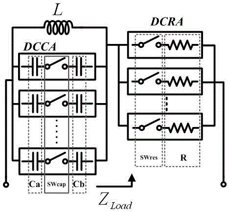
本发明提供一种的宽带可重构负载网络,如图1中所示,由电感L、电压控制电容阵列DCCA和电压控制电阻阵列DCRA组成;所述电压控制电容阵列与所述电感并联构成LC并联谐振网络,该谐振网络顺次与所述电压控制电阻阵列串联,构成RLC负载网络;通过电压控制电容阵列开关,调整谐振频率;通过电压控制电阻阵列的开关,调整不同频段下的增益。 The present invention provides a wideband reconfigurable load network, as shown in Figure 1, consisting of an inductor L, a voltage-controlled capacitor array DCCA and a voltage-controlled resistor array DCRA; the voltage-controlled capacitor array is connected in parallel with the inductor to form an LC A parallel resonant network, the resonant network is connected in series with the voltage-controlled resistor array in sequence to form an RLC load network; the resonant frequency is adjusted through the voltage-controlled switch of the capacitor array; and the gain under different frequency bands is adjusted through the switch of the voltage-controlled resistor array.
进一步地,如图1中所示,该电压控制电容阵列DCCA中的每一列电容阵列均由电容Ca连接开关SWcap,然后顺次连接电容Cb组成,这样的电容阵列多级并联组成上述电压控制电容阵列。 Further, as shown in FIG. 1, each column of the capacitor array in the voltage control capacitor array DCCA is composed of a capacitor Ca connected to a switch SWcap, and then connected to a capacitor Cb in sequence. Such capacitor arrays are connected in parallel in multiple stages to form the voltage control capacitor array.
进一步地,如图1中所示,该电压控制电阻阵列DCRA中的每一列电阻阵列均由开关SWres连接电阻R组成,这样的电阻阵列多级并联组成上述电压控制电阻阵列。 Further, as shown in FIG. 1 , each column of the resistor array in the voltage-controlled resistor array DCRA is composed of a switch SWres connected to a resistor R, and such resistor arrays are connected in parallel in multiple stages to form the above-mentioned voltage-controlled resistor array.
进一步地,如图2中所示,通过开关的关断打开不同组合,实现所述负载网络的谐振点的可重构。 Further, as shown in FIG. 2 , by turning off the switches to open different combinations, the reconfigurability of the resonance point of the load network is realized.
进一步地,为了解决图1中所示的在低频处负载阻抗Zload较低的问题,通过改变控制电压控制电阻阵列DCRA的开关关断、打开组合,增大电压控制电阻阵列DCRA阵列的阻值,提高低频处的负载阻抗Zload;通过降低电压控制电阻阵列DCRA阵列的等效阻值,增加高频处的负载阻抗Zload。实现效果如图3和图4所示。 Further, in order to solve the problem of lower load impedance Z load at low frequencies as shown in Figure 1, by changing the switch off and on combination of the control voltage control resistor array DCRA, the resistance value of the voltage control resistor array DCRA array is increased , increase the load impedance Z load at low frequency; increase the load impedance Z load at high frequency by reducing the equivalent resistance of the voltage control resistor array DCRA array. The realization effect is shown in Figure 3 and Figure 4.
本发明的改进主要体现在: Improvement of the present invention is mainly reflected in:
1、提出一种新型的宽带可重构负载网络,可以通过改变DCCA和DCRA控制电压实现负载网络工作于不同频段上,覆盖范围从1.8~10.6GHz,可以覆盖现有的主要通信标准。 1. A new type of broadband reconfigurable load network is proposed, which can realize the load network to work in different frequency bands by changing the control voltage of DCCA and DCRA. The coverage range is from 1.8 to 10.6GHz, which can cover the existing main communication standards.
2、研究了RLC网络的特性,利用在高、低频处不同网络参数值对应的不同等效负载网络阻抗值Zload特点来调整不同标准下的Zload; 2. Study the characteristics of the RLC network, and adjust the Z load under different standards by using the characteristics of different equivalent load network impedance values Z load corresponding to different network parameter values at high and low frequencies;
3、所述网络只使用了一个电感,就可以覆盖频带从1.8~10.6GHz,节省了面积。 3. The network only uses one inductor, which can cover the frequency band from 1.8 to 10.6 GHz, saving the area.
本发明的负载网络具有结构简单,灵活可重构特点,可以针对不同应用进行数字控制,使负载网络工作在不同频率上。特别应用于1.8~10.6GHz的多模接收机前端低噪声放大器和混频器的负载中。适用于包括GSM、LTE、WCDMA、Bluetooth、WLAN、UWB等多模接收机系统中。 The load network of the present invention has the characteristics of simple structure, flexibility and reconfiguration, and can carry out digital control for different applications, so that the load network can work at different frequencies. It is especially used in the load of low-noise amplifiers and mixers at the front end of multi-mode receivers at 1.8~10.6GHz. It is suitable for multi-mode receiver systems including GSM, LTE, WCDMA, Bluetooth, WLAN, UWB, etc.
附图说明 Description of drawings
图1:本发明宽带可重构负载网络的设计实例框图。 Fig. 1: A block diagram of a design example of a broadband reconfigurable load network of the present invention.
图2:本发明宽带可重构负载网络改变DCCA的等效电容值对Zload的影响。 Fig. 2: The effect of changing the equivalent capacitance value of DCCA on Z load in the broadband reconfigurable load network of the present invention.
图3:本发明宽带可重构负载网络改变DCRA来配合DCCA实现低频处的增益提高效果。 Figure 3: The wideband reconfigurable load network of the present invention changes DCRA to cooperate with DCCA to achieve gain improvement at low frequencies.
图4:本发明宽带可重构负载网络改变DCRA来配合DCCA实现高频处的增益提高效果。 Figure 4: The wideband reconfigurable load network of the present invention changes DCRA to cooperate with DCCA to achieve gain improvement at high frequencies.
具体实施方式 Detailed ways
下面通过实施例结合附图进一步描述本发明。 Further describe the present invention below by embodiment in conjunction with accompanying drawing. the
如图1所示,通过对开关电压的选择,所述负载网络可以在1.8~10.6GHz频段内变化等效阻抗值Zload ,以满足各通信标准的要求,可以实现可变增益可变带宽的可重构。 As shown in Figure 1, by selecting the switching voltage, the load network can change the equivalent impedance value Z load in the 1.8-10.6 GHz frequency band to meet the requirements of various communication standards and realize variable gain and variable bandwidth. reconfigurable.
最后应说明的是,以上仅用以说明本发明的技术方案而非限制,本领域的普通技术人员应当理解,可以对本发明的技术方案进行修改或者等同替换,而不脱离本发明技术方案的精神和范围,其均应涵盖在本发明的权利要求范围中。 Finally, it should be noted that the above is only used to illustrate the technical solution of the present invention rather than limit it. Those of ordinary skill in the art should understand that the technical solution of the present invention can be modified or equivalently replaced without departing from the spirit of the technical solution of the present invention and scope, which should be included in the scope of the claims of the present invention.
Claims (3)
Priority Applications (1)
| Application Number | Priority Date | Filing Date | Title |
|---|---|---|---|
| CN2011102063834A CN102386874A (en) | 2011-07-22 | 2011-07-22 | Wideband reconfigurable load network |
Applications Claiming Priority (1)
| Application Number | Priority Date | Filing Date | Title |
|---|---|---|---|
| CN2011102063834A CN102386874A (en) | 2011-07-22 | 2011-07-22 | Wideband reconfigurable load network |
Publications (1)
| Publication Number | Publication Date |
|---|---|
| CN102386874A true CN102386874A (en) | 2012-03-21 |
Family
ID=45825916
Family Applications (1)
| Application Number | Title | Priority Date | Filing Date |
|---|---|---|---|
| CN2011102063834A Pending CN102386874A (en) | 2011-07-22 | 2011-07-22 | Wideband reconfigurable load network |
Country Status (1)
| Country | Link |
|---|---|
| CN (1) | CN102386874A (en) |
Cited By (3)
| Publication number | Priority date | Publication date | Assignee | Title |
|---|---|---|---|---|
| CN104459393A (en) * | 2014-12-05 | 2015-03-25 | 国家电网公司 | Large-capacity adjustable simulation RLC test load |
| CN110719074A (en) * | 2019-09-23 | 2020-01-21 | 成都航天科工微电子系统研究院有限公司 | A Tunable Broadband Low Noise Amplifier |
| CN111416586A (en) * | 2020-04-03 | 2020-07-14 | 杭州易百德微电子有限公司 | Load structure and radio frequency amplifier formed by same |
Citations (5)
| Publication number | Priority date | Publication date | Assignee | Title |
|---|---|---|---|---|
| CN101496287A (en) * | 2006-06-15 | 2009-07-29 | 比特沃半导体公司 | Continuous gain compensation and fast band selection in a multi-standard, multi-frequencey synthesizer |
| CN101753159A (en) * | 2010-01-11 | 2010-06-23 | 清华大学 | RF (radio frequency) receiving front end with diversified gaining modes and capable of automatic tuning |
| CN101834576A (en) * | 2010-04-08 | 2010-09-15 | 复旦大学 | Multimode Tunable CMOS Differential Low Noise Amplifier |
| US20100290368A1 (en) * | 2009-05-14 | 2010-11-18 | Texas Instruments Deutschland Gmbh | Half-duplex rfid transponder and a method of operating a half-duplex rfid transponder |
| CN102006095A (en) * | 2010-10-21 | 2011-04-06 | 华东师范大学 | Automatic frequency calibration channel selection filter for multi-frequency multi-mode wireless transceiver |
-
2011
- 2011-07-22 CN CN2011102063834A patent/CN102386874A/en active Pending
Patent Citations (5)
| Publication number | Priority date | Publication date | Assignee | Title |
|---|---|---|---|---|
| CN101496287A (en) * | 2006-06-15 | 2009-07-29 | 比特沃半导体公司 | Continuous gain compensation and fast band selection in a multi-standard, multi-frequencey synthesizer |
| US20100290368A1 (en) * | 2009-05-14 | 2010-11-18 | Texas Instruments Deutschland Gmbh | Half-duplex rfid transponder and a method of operating a half-duplex rfid transponder |
| CN101753159A (en) * | 2010-01-11 | 2010-06-23 | 清华大学 | RF (radio frequency) receiving front end with diversified gaining modes and capable of automatic tuning |
| CN101834576A (en) * | 2010-04-08 | 2010-09-15 | 复旦大学 | Multimode Tunable CMOS Differential Low Noise Amplifier |
| CN102006095A (en) * | 2010-10-21 | 2011-04-06 | 华东师范大学 | Automatic frequency calibration channel selection filter for multi-frequency multi-mode wireless transceiver |
Cited By (4)
| Publication number | Priority date | Publication date | Assignee | Title |
|---|---|---|---|---|
| CN104459393A (en) * | 2014-12-05 | 2015-03-25 | 国家电网公司 | Large-capacity adjustable simulation RLC test load |
| CN110719074A (en) * | 2019-09-23 | 2020-01-21 | 成都航天科工微电子系统研究院有限公司 | A Tunable Broadband Low Noise Amplifier |
| CN110719074B (en) * | 2019-09-23 | 2023-06-20 | 航天科工微电子系统研究院有限公司 | Tunable broadband low noise amplifier |
| CN111416586A (en) * | 2020-04-03 | 2020-07-14 | 杭州易百德微电子有限公司 | Load structure and radio frequency amplifier formed by same |
Similar Documents
| Publication | Publication Date | Title |
|---|---|---|
| US11444593B2 (en) | Method and apparatus for adapting a variable impedance network | |
| CN104242829B (en) | With based on the relevant circuit of the approximate efficiency power amplifier of multiple-harmonic and method | |
| CN203219248U (en) | A kind of LTE radio frequency power amplifier | |
| CN108736835B (en) | Multi-band low-power-consumption low-noise amplifier | |
| TW201931785A (en) | Circuits and methods related to radio-frequency receivers having carrier aggregation | |
| ATE430371T1 (en) | VARIABLE INTEGRATED INDUCTIVITY | |
| US20190089323A1 (en) | Impedance matching circuit, radio-frequency front-end circuit, and communication device | |
| CN203522706U (en) | Multi-band frequency source | |
| CN101938256B (en) | Fully integrated dual-band configurable radio-frequency power amplifier | |
| CN102386874A (en) | Wideband reconfigurable load network | |
| JP2011155357A (en) | Multi-band power amplifier | |
| Slimane et al. | A reconfigurable inductor-less CMOS low noise amplifier for multi-standard applications | |
| WO2014050721A2 (en) | Amplifying device, and wireless communication device equipped with amplifying device | |
| CN105281673A (en) | Multi-band reconfigurable mixing method and mixer | |
| KR101396630B1 (en) | Tunable Capacitance Control Circuit and Tunable Capacitance Control Method | |
| Suvarna et al. | Transformer-based tunable matching network design techniques in 40-nm CMOS | |
| CN105099479A (en) | Radio-frequency front-end circuit of multi-mode intelligent terminal receiver | |
| KR101353175B1 (en) | Variable capacitor module | |
| CN202385062U (en) | Radio frequency filter based on variable transconductance operational amplifier | |
| KR101699375B1 (en) | To support multiple frequency bands matching circuit | |
| Slimane et al. | A 0.6-V/1.2-V low power single ended CMOS LNA for multi-standard RF front-ends | |
| Zhang et al. | Dual SPDT/SP3T SOI CMOS switch adopting alternative bias strategy with enhanced performance compared to the conventional case | |
| JP2010232957A (en) | Variable impedance matching circuit | |
| Chen et al. | RF Front-End and Complex BPF for Reconfigurable Low-IF Receiver | |
| Collot et al. | Reconfigurable filtering differential low noise amplifier using MEMS tunable inductor |
Legal Events
| Date | Code | Title | Description |
|---|---|---|---|
| C06 | Publication | ||
| PB01 | Publication | ||
| C10 | Entry into substantive examination | ||
| SE01 | Entry into force of request for substantive examination | ||
| C12 | Rejection of a patent application after its publication | ||
| RJ01 | Rejection of invention patent application after publication |
Application publication date: 20120321 |