CN102263170A - Light emitting device and light emitting device package - Google Patents
Light emitting device and light emitting device package Download PDFInfo
- Publication number
- CN102263170A CN102263170A CN2011101470960A CN201110147096A CN102263170A CN 102263170 A CN102263170 A CN 102263170A CN 2011101470960 A CN2011101470960 A CN 2011101470960A CN 201110147096 A CN201110147096 A CN 201110147096A CN 102263170 A CN102263170 A CN 102263170A
- Authority
- CN
- China
- Prior art keywords
- layer
- light emitting
- emitting device
- luminescent device
- type semiconductor
- Prior art date
- Legal status (The legal status is an assumption and is not a legal conclusion. Google has not performed a legal analysis and makes no representation as to the accuracy of the status listed.)
- Pending
Links
Images


Classifications
-
- H—ELECTRICITY
- H10—SEMICONDUCTOR DEVICES; ELECTRIC SOLID-STATE DEVICES NOT OTHERWISE PROVIDED FOR
- H10H—INORGANIC LIGHT-EMITTING SEMICONDUCTOR DEVICES HAVING POTENTIAL BARRIERS
- H10H20/00—Individual inorganic light-emitting semiconductor devices having potential barriers, e.g. light-emitting diodes [LED]
- H10H20/80—Constructional details
- H10H20/83—Electrodes
- H10H20/832—Electrodes characterised by their material
-
- H—ELECTRICITY
- H10—SEMICONDUCTOR DEVICES; ELECTRIC SOLID-STATE DEVICES NOT OTHERWISE PROVIDED FOR
- H10H—INORGANIC LIGHT-EMITTING SEMICONDUCTOR DEVICES HAVING POTENTIAL BARRIERS
- H10H20/00—Individual inorganic light-emitting semiconductor devices having potential barriers, e.g. light-emitting diodes [LED]
- H10H20/01—Manufacture or treatment
- H10H20/011—Manufacture or treatment of bodies, e.g. forming semiconductor layers
- H10H20/018—Bonding of wafers
-
- H—ELECTRICITY
- H10—SEMICONDUCTOR DEVICES; ELECTRIC SOLID-STATE DEVICES NOT OTHERWISE PROVIDED FOR
- H10H—INORGANIC LIGHT-EMITTING SEMICONDUCTOR DEVICES HAVING POTENTIAL BARRIERS
- H10H20/00—Individual inorganic light-emitting semiconductor devices having potential barriers, e.g. light-emitting diodes [LED]
- H10H20/80—Constructional details
- H10H20/81—Bodies
- H10H20/819—Bodies characterised by their shape, e.g. curved or truncated substrates
- H10H20/82—Roughened surfaces, e.g. at the interface between epitaxial layers
-
- H—ELECTRICITY
- H10—SEMICONDUCTOR DEVICES; ELECTRIC SOLID-STATE DEVICES NOT OTHERWISE PROVIDED FOR
- H10H—INORGANIC LIGHT-EMITTING SEMICONDUCTOR DEVICES HAVING POTENTIAL BARRIERS
- H10H20/00—Individual inorganic light-emitting semiconductor devices having potential barriers, e.g. light-emitting diodes [LED]
- H10H20/80—Constructional details
- H10H20/81—Bodies
- H10H20/822—Materials of the light-emitting regions
- H10H20/824—Materials of the light-emitting regions comprising only Group III-V materials, e.g. GaP
- H10H20/825—Materials of the light-emitting regions comprising only Group III-V materials, e.g. GaP containing nitrogen, e.g. GaN
-
- H—ELECTRICITY
- H10—SEMICONDUCTOR DEVICES; ELECTRIC SOLID-STATE DEVICES NOT OTHERWISE PROVIDED FOR
- H10H—INORGANIC LIGHT-EMITTING SEMICONDUCTOR DEVICES HAVING POTENTIAL BARRIERS
- H10H20/00—Individual inorganic light-emitting semiconductor devices having potential barriers, e.g. light-emitting diodes [LED]
- H10H20/80—Constructional details
- H10H20/83—Electrodes
- H10H20/831—Electrodes characterised by their shape
-
- H—ELECTRICITY
- H10—SEMICONDUCTOR DEVICES; ELECTRIC SOLID-STATE DEVICES NOT OTHERWISE PROVIDED FOR
- H10H—INORGANIC LIGHT-EMITTING SEMICONDUCTOR DEVICES HAVING POTENTIAL BARRIERS
- H10H20/00—Individual inorganic light-emitting semiconductor devices having potential barriers, e.g. light-emitting diodes [LED]
- H10H20/80—Constructional details
- H10H20/83—Electrodes
- H10H20/832—Electrodes characterised by their material
- H10H20/835—Reflective materials
-
- H10W90/756—
Landscapes
- Led Devices (AREA)
Abstract
本发明提供一种发光器件和发光器件封装。该发光器件包括:发光结构层,该发光结构层包括第一导电类型半导体层、有源层以及第二导电类型半导体层;在发光结构层上的镓阻挡层;以及在镓阻挡层上的金属电极层。
The invention provides a light emitting device and a light emitting device package. The light emitting device includes: a light emitting structure layer, the light emitting structure layer including a first conductivity type semiconductor layer, an active layer and a second conductivity type semiconductor layer; a gallium blocking layer on the light emitting structure layer; and a metal layer on the gallium blocking layer electrode layer.
Description
技术领域 technical field
本发明涉及一种发光器件、制造发光器件的方法、发光器件封装、以及照明系统。The present invention relates to a light emitting device, a method for manufacturing the light emitting device, a package of the light emitting device, and a lighting system.
背景技术 Background technique
由于其物理和化学特性,III-V族氮化物半导体被关注作为发光二极管(LED)或者激光二极管(LD)的核心材料。通常,III-V族氮化物半导体由具有InxAlyGa1-x-yN(0≤x≤1,0≤y≤1,0≤x+y≤1)的组成式的半导体材料形成。Due to their physical and chemical properties, group III-V nitride semiconductors are of interest as core materials for light emitting diodes (LEDs) or laser diodes (LDs). Generally, a group III-V nitride semiconductor is formed of a semiconductor material having a composition formula of InxAlyGa1 -xyN (0≤x≤1, 0≤y≤1, 0≤x+y≤1).
这样的LED使用化合物半导体的特性将电信号转换为诸如红外线、紫外线或者可见光的光。最近,随着LED的光效率增加,在诸如显示装置和照明装置的各种领域中使用LED。Such LEDs convert electrical signals into light such as infrared rays, ultraviolet rays, or visible light using properties of compound semiconductors. Recently, as the light efficiency of LEDs increases, LEDs are used in various fields such as display devices and lighting devices.
发明内容 Contents of the invention
实施例提供具有新结构的发光器件、制造发光器件的方法、发光器件封装、以及照明系统。Embodiments provide a light emitting device having a new structure, a method of manufacturing a light emitting device, a light emitting device package, and a lighting system.
实施例还提供具有改进的可靠性的发光器件、制造发光器件的方法、发光器件封装、以及照明系统。Embodiments also provide a light emitting device having improved reliability, a method of manufacturing a light emitting device, a light emitting device package, and a lighting system.
在一个实施例中,发光器件包括:发光结构层,该发光结构层包括第一导电类型半导体层、有源层以及第二导电类型半导体层;在发光结构层上的镓阻挡层;以及在镓阻挡层上的金属电极层。In one embodiment, a light emitting device includes: a light emitting structure layer including a first conductivity type semiconductor layer, an active layer, and a second conductivity type semiconductor layer; a gallium blocking layer on the light emitting structure layer; The metal electrode layer on the barrier layer.
在另一实施例中,发光器件封装包括:主体;第一和第二电极层,该第一和第二电极层被布置在主体上,以及发光器件,所述发光器件被布置在所述主体上并且电连接到第一和第二电极层,其中所述发光器件包括:发光结构层,该发光结构层包括第一导电类型半导体层、有源层以及第二导电类型半导体层;在发光结构层上的镓阻挡层;以及在镓阻挡层上的金属电极层。In another embodiment, a light emitting device package includes: a main body; first and second electrode layers disposed on the main body, and a light emitting device disposed on the main body and electrically connected to the first and second electrode layers, wherein the light emitting device includes: a light emitting structure layer, the light emitting structure layer includes a first conductivity type semiconductor layer, an active layer and a second conductivity type semiconductor layer; a gallium barrier layer on the gallium barrier layer; and a metal electrode layer on the gallium barrier layer.
在附图和下面的描述中,阐述一个或者多个实施例的细节。根据描述和附图以及权利要求,其它的特征将会是显而易见的。The details of one or more implementations are set forth in the accompanying drawings and the description below. Other features will be apparent from the description and drawings, and from the claims.
附图说明 Description of drawings
图1是根据实施例的发光器件的截面图。FIG. 1 is a cross-sectional view of a light emitting device according to an embodiment.
图2至图13是示出制造根据实施例的发光器件的工艺的视图。2 to 13 are views illustrating a process of manufacturing a light emitting device according to an embodiment.
图14是包括根据实施例的发光器件的发光器件封装的截面图。FIG. 14 is a cross-sectional view of a light emitting device package including the light emitting device according to the embodiment.
图15是包括根据实施例的发光器件封装的背光单元的视图。FIG. 15 is a view of a backlight unit including the light emitting device package according to the embodiment.
图16是包括根据实施例的发光器件封装的照明单元的透视图。FIG. 16 is a perspective view of a lighting unit including the light emitting device package according to the embodiment.
具体实施方式 Detailed ways
在实施例的描述中,将会理解的是,当层(或膜)、区域、图案或结构被称为在衬底、层(或膜)、区域、焊盘或图案“上”时,它能够直接地在另一层或者衬底上,或者也可以存在中间层。此外,将会理解的是,当层被称为在另一层“下”时,它能够直接地在另一层下,并且也可以存在一个或者多个中间层。此外,将基于附图来进行对关于每层“上”和“下”的参考。In the description of embodiments, it will be understood that when a layer (or film), region, pattern or structure is referred to as being "on" a substrate, layer (or film), region, pad or pattern, it It can be directly on another layer or substrate, or intervening layers can also be present. Further, it will be understood that when a layer is referred to as being 'under' another layer, it can be directly under another layer, and one or more intervening layers may also be present. In addition, reference to 'on' and 'under' each layer will be made based on the drawings.
在附图中,为了描述的方便和清楚起见,每层的厚度或者尺寸被夸大、省略或示意性绘制。而且,每个元件的尺寸没有完全反映真实尺寸。In the drawings, the thickness or size of each layer is exaggerated, omitted, or schematically drawn for convenience and clarity of description. Also, the size of each element does not completely reflect an actual size.
在下文中,将会参考附图描述发光器件、制造发光器件的方法、发光器件封装以及照明系统。Hereinafter, a light emitting device, a method of manufacturing a light emitting device, a light emitting device package, and a lighting system will be described with reference to the accompanying drawings.
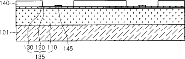
图1是根据实施例的发光器件100的截面图。FIG. 1 is a cross-sectional view of a
参考图1,根据实施例的发光器件100可以包括:导电支撑构件175;发光结构层135,该发光结构层135被布置在导电支撑构件175上以产生光并且在其顶表面的一部分上具有光提取图案112;电极115,该电极115被布置在发光结构层135上并且包括镓阻挡层113和金属电极层114;以及保护层180,该保护层180被布置在发光结构层135的顶表面和侧表面上。Referring to FIG. 1 , a
保护构件140、欧姆层150、反射层160、粘附层170、以及电流阻挡层145可以被布置在导电支撑构件175和发光结构层135之间。The
发光结构层135可以包括第一导电类型半导体层110、有源层120以及第二导电类型半导体层130。从第一和第二导电类型半导体层110和130提供的电子和空穴可以在有源层120中复合以产生光。The light
导电支撑构件175可以支撑发光结构层135并且与电极115一起将电力提供到发光结构层135。例如,导电支撑构件175可以由其中注入杂质的载体晶片(例如,Si、Ge、GaN、GaAs、ZnO、SiC、SiGe等等)、Ti、Cr、Ni、Al、Pt、Au、W、Cu、Mo以及Cu-W中的至少一个形成。导电支撑构件175可以具有根据发光器件100的设计而变化的厚度。例如,导电支撑构件175可以具有大约30μm至大约500μm的厚度。The
粘附层170可以被布置在导电支撑构件175上。粘附层170可以是结合层并且被布置在反射层160和保护构件140下面。粘附层170的外表面可以被暴露以接触反射层160、欧姆层150的末端以及保护构件140,从而增强这些层之间的粘附力。The
粘附层170可以由阻挡金属或者结合金属形成。例如,粘附层170可以由Ti、Au、Sn、Ni、Cr、Ga、In、Bi、Cu、Al、Si、Ag以及Ta中的至少一个形成。The
反射层160可以被布置在粘附层170上。反射层160可以反射从发光结构层135入射的光以提高发光器件100的发光效率。The
反射层160可以由具有高反射率的金属材料形成,例如,由包括Ag、Ni、Al、Rh、Pd、Ir、Ru、Mg、Zn、Pt、Au、Cu以及Hf中的至少一个的金属或者合金形成。替代地,反射层160可以具有使用该金属或者合金以及诸如IZO、IZTO、IAZO、IGZO、IGTO、AZO以及ATO的透明导电材料形成的多层结构。例如,反射层160可以由IZO/Ni、AZO/Ag、IZO/Ag/Ni、AZO/Ag/Ni、Ag/Cu以及Ag/Pd/Cu形成。The
欧姆层150可以被布置在反射层160上。欧姆层150可以欧姆接触第二导电类型半导体层130以将电力平滑地提供到发光结构层135。The
欧姆层150可以选择性地使用透明导电层和金属。例如,通过使用铟锡氧化物(ITO)、铟锌氧化物(IZO)、铟锌锡氧化物(IZTO)、铟铝锌氧化物(IAZO)、铟镓锌氧化物(IGZO)、铟镓锡氧化物(IGTO)、铝锌氧化物(AZO)、锑锡氧化物(ATO)、镓锌氧化物(GZO)、IrOx、RuOx、RuOx/ITO、Ni、Ag、Pt、Ni/IrOx/Au以及Ni/IrOx/Au/ITO中的至少一个可以将欧姆层150实现为单或者多层。The
电流阻挡层(CBL)145可以被布置在欧姆层150和第二导电类型半导体层130之间。CBL 145的至少部分可以垂直地重叠电极115。因此,可以减少其中电流被集中到电极115和导电支撑构件175之间的最短距离的现象以提高发光器件100的发光效率。A current blocking layer (CBL) 145 may be disposed between the
CBL 145可以由具有绝缘性的材料、具有小于反射层160或者粘附层170的导电性的导电性的材料、以及肖特基接触第二导电类型半导体层130的材料中的至少一个形成。例如,CBL 145可以由ITO、IZO、IZTO、IAZO、IGZO、IGTO、AZO、ATO、ZnO、SiO2、SiOx、SiOxNy、Si3N4、Al2O3、TiOx、TiO2、Ti、Al以及Cr中的至少一个形成。The CBL 145 may be formed of at least one of a material having insulating properties, a material having conductivity less than that of the
CBL 145可以被布置在反射层160和欧姆层150之间,但是不限于此。The CBL 145 may be disposed between the
保护构件140可以被布置在粘附层170的顶表面的外周上。保护构件140可以被布置在第二导电类型半导体层130的底表面的外周上。即,保护构件140可以具有环形、回路形状、或者框架形状。保护构件140可以接触第二导电类型半导体层130并且具有位于发光器件100内的环形、回路形状、或者框架形状。The
保护构件140可以最小化发光结构层135和导电支撑构件175之间的电气短路的发生。而且,保护构件140可以防止湿气渗透通过发光结构层135和导电支撑构件175之间的间隙。The
保护构件140可以由具有绝缘性的材料、具有小于反射层160或者粘附层170的导电性的导电性的材料、以及肖特基接触第二导电类型半导体层130的材料中的至少一个形成。例如,保护构件140可以由ITO、IZO、IZTO、IAZO、IGZO、IGTO、AZO、ATO、ZnO、SiO2、SiOx、SiOxNy、Si3N4、Al2O3、TiOx、TiO2、Ti、Al以及Cr中的至少一个形成。The
发光结构层135可以被布置在欧姆层150和保护构件140之间。The light emitting
发光结构层135可以包括多个III-V族化合物半导体层。例如,发光结构135可以包括第一导电类型半导体层110、被布置在第一导电类型半导体层110下面的有源层120以及被布置在有源层120下面的第二导电类型半导体层130。The light emitting
第一导电类型半导体层110可以是其中掺杂第一导电类型掺杂物的III-V族化合物半导体,并且通过InxAlyGa1-x-yN(0≤x≤1,0≤y≤1,0≤x+y≤1)的组成式来实现。而且,第一导电类型半导体层110可以由GaN、AlN、AlGaN、InGaN、InN、InAlGaN、AlInN、AlGaAs、GaP、GaAs、GaAsP以及AlGaInP中的一个形成。当第一导电半导体层110是N型半导体层时,第一导电类型掺杂物可以包括诸如Si、Ge、Sn、Se或者Te的N型掺杂物。第一导电类型半导体层110可以具有单或者多层结构,但是不限于此。The first conductivity
有源层120可以被布置在第一导电类型半导体层110下面。有源层120可以具有单量子阱结构、多量子阱(MQW)结构、量子线结构以及量子点结构中的一个。例如,有源层120可以具有使用III-V族元素的化合物半导体材料的阱层和势垒层的周期,例如,InGaN阱层/GaN势垒层的周期或者InGaN阱层/AlGaN势垒层的周期。The
导电类型包覆层可以被布置在有源层120上或/和下面。导电类型包覆层可以由AlGaN基半导体形成。A conductive type cladding layer may be disposed on or/and under the
第二导电类型半导体层130可以被布置在有源层120下面。而且,第二导电类型半导体层130可以是其中掺杂第二导电类型掺杂物的III-V族化合物半导体并且通过InxAlyGa1-x-yN(0≤x≤1,0≤y≤1,0≤x+y≤1)的组成式来实现。而且,第二导电类型半导体层130可以由GaN、AlN、AlGaN、InGaN、InN、InAlGaN、AlInN、AlGaAs、GaP、GaAs、GaAsP以及AlGaInP中的一个形成。当第二导电半导体层110是P型半导体层时,第二导电类型掺杂物可以包括诸如Mg或者Zn的P型掺杂物。The second conductive
发光结构层135可以进一步包括在第二导电类型半导体层130下面的具有与第二导电类型半导体层130的极性相反的极性的半导体层。而且,可以通过P型半导体层实现第一导电类型半导体层110,并且可以通过N型半导体层实现第二导电类型半导体层130。因此,发光结构层135可以具有N-P结结构、P-N结结构、N-P-N结结构以及P-N-P结结构中的至少一个。The light emitting
通过隔离蚀刻工艺,发光结构层135可以具有倾斜的侧表面,以将多个芯片划分为单独的芯片单元。Through the isolation etching process, the light emitting
而且,光提取图案112可以被布置在发光结构层135的顶表面上。光提取图案112可以减少从发光结构层135发射的光被全反射而没有被提取到外部的光的量。因此,可以提高发光器件100的光提取效率。Also, the
光提取图案112和保护层180可以相互部分地垂直重叠。因此,可以最大化发光器件100的光提取效率,并且它可以防止保护层180和第一导电类型半导体层110容易地相互分离。因此,可以提高发光器件100的可靠性。The
光提取图案112可以具有随机的形状和布置或者想要的形状和布置。The
例如,光提取图案112可以被布置有具有大约50nm至大约3000nm的周期的光子晶体结构。光子晶体结构可以通过干涉效应将具有特定波长的光有效地提取到外部。For example, the
而且,光提取图案112可以具有诸如圆柱形、多边柱形、圆锥形状、多棱锥形状、截锥形状、以及棱锥台形状(polygonal cone shape)的形状。Also, the
电极115可以被布置在发光结构层135的顶表面上。电极115可以以预定的图案形状分支,但是不限于此。The
电极115可以接触第一导电类型半导体层110的顶表面。当第一导电类型半导体层110是GaN层时,电极115可以接触第一导电类型半导体层110的顶表面,即,N面表面。电极115可以包括接触第一导电类型半导体层110的镓阻挡层113和被布置在镓阻挡层113上的金属电极层114。The
而且,电极115可以具有其中至少一个焊盘和具有至少一种形状并且被连接到焊盘的电极图案彼此相等或者相互不同地堆叠的结构,但是不限于此。Also, the
由于镓的扩散使得可以在第一导电类型半导体层110的顶表面,即,N面表面中限定孔。因此,N/Ga的比率可以增加以引起非欧姆接触。因此,其中掺杂镓的镓阻挡层113可以被布置在第一导电类型半导体层110上以改进发光器件100的电气特性。Holes may be defined in the top surface of the first conductive
镓阻挡层113可以由其中掺杂镓的金属形成。金属可以包括Al、Ti、Ta、Cr、Mn、V、Nb、Hf、Zr以及Zn中的至少一个。可以以一定的浓度将镓掺杂到金属中,例如,如果金属是Al,则浓度为金属的总重量比率的大约1%至大约17%;如果金属是Ti,则浓度为金属的总重量比率的大约1%至大约14%;如果金属是Ta,则浓度为金属的总重量比率的大约1%至大约14%;如果金属是Cr,则浓度为金属的总重量比率的大约1%至大约15%;如果金属是Mn,则浓度为金属的总重量比率的大约1%至大约10%;如果金属是V,则浓度为金属的总重量比率的大约1%至大约15%;如果金属是Nb,则浓度为金属的总重量比率的大约1%至大约5%;如果金属是Hf,则浓度为金属的总重量比率的大约0.3%至大约3%;如果金属是Zr,则浓度为金属的总重量比率的大约0.2%至大约1%;并且如果金属是Zn,则浓度为金属的总重量比率的大约0.5%至大约4%。The
金属电极层114可以由Cr、Ni、Au、Ti以及Al中的至少一个形成。The
保护层180可以被布置在发光结构层135的顶表面和侧表面上。The
保护层180可以防止发光结构层135与外部电极电气地短路。保护层180可以由具有绝缘性和透射性的材料形成,例如,由SiO2、SiOx、SiOxNy、Si3N4、TiO2以及Al2O3中的至少一个材料形成。The
保护层180可以被设置在除了其中布置电极115的区域之外的发光结构层135上面的区域中。而且,保护层180可以被布置在除了其中布置发光结构层135的光提取图案112的区域之外的区域中。The
根据实施例的发光器件100具有垂直型电极结构。因此,由于器件工艺的特性使得可以以低温热处理发光器件100。例如,当在小于大约250℃的温度执行热处理工艺时,在电极115仅包括金属电极层114而不包括镓阻挡层113的情况下,电极115具有非欧姆接触特性。The
根据实施例的发光器件100包括镓阻挡层113。因此,它可以防止第一导电类型半导体层110的Ga扩散,并且在没有在高温执行热处理工艺的情况下可以实现欧姆接触。The
在下文中,将会参考图2至图13详细地描述制造根据实施例的发光器件100的方法。然而,将会省略或者简要地描述上述元件的构成的描述。Hereinafter, a method of manufacturing the
参考图2,发光结构层135可以形成在生长衬底101上。Referring to FIG. 2 , a light emitting
例如,生长衬底101可以由蓝宝石(Al2O3)、SiC、GaN、Si、ZnO、Si、GaP、InP以及Ge中的至少一个形成,但是不限于此。For example, the
第一导电类型半导体层110、有源层120以及第二导电类型半导体层130可以顺序地生长在生长衬底101上以形成发光结构层135。The first conductive
例如,使用金属有机化学气相沉积(MOCVD)工艺、化学气相沉积(CVD)工艺、等离子体增强化学气相沉积(PECVD)工艺、分子束外延(MBE)工艺、或者氢化物气相外延(HVPE)工艺可以形成发光结构层,但是不限于此。For example, using a metal organic chemical vapor deposition (MOCVD) process, a chemical vapor deposition (CVD) process, a plasma enhanced chemical vapor deposition (PECVD) process, a molecular beam epitaxy (MBE) process, or a hydride vapor phase epitaxy (HVPE) process can A light emitting structure layer is formed, but not limited thereto.
缓冲层可以形成在发光结构层135和生长衬底101之间以减少其间的晶格常数差。A buffer layer may be formed between the light emitting
参考图3,可以在发光结构层135上沿着芯片边界区域形成保护构件140。Referring to FIG. 3 , a
可以使用构图的掩模在单独的芯片区域的外周上形成保护构件140。保护构件140可以具有环形、回路形状、或者框架形状。例如,可以通过电子束沉积工艺、溅射工艺或者等离子体增强化学气相沉积(PECVD)工艺来形成保护构件140。The
例如,保护构件140可以由ITO、IZO、IZTO、IAZO、IGZO、IGTO、AZO、ATO、ZnO、SiO2、SiOx、SiOxNy、Si3N4、Al2O3、TiOx、TiO2、Ti、Al以及Cr中的至少一个形成。For example, the
参考图4,电流阻挡层(CBL)145可以形成在第二导电类型半导体层上。使用构图的掩模可以形成CBL 135。Referring to FIG. 4 , a current blocking layer (CBL) 145 may be formed on the second conductive type semiconductor layer.
CBL 135可以被布置在其处CBL 145的至少一部分垂直地重叠以后形成的电极115的位置上。结果,可以减少其中电流被集中到发光结构层135内的特定区域中的现象。
参考图5和图6,欧姆层150可以形成在第二导电类型半导体层130和CBL 145上。反射层160可以被形成在欧姆层150上。Referring to FIGS. 5 and 6 , an
例如,可以使用电子束沉积工艺、溅射工艺以及等离子体增强化学气相沉积(PECVD)工艺形成欧姆层150和反射层160。For example, the
参考图7,粘附层170可以形成在保护构件140上。导电支撑构件175可以形成在粘附层170上。Referring to FIG. 7 , an
粘附层170可以形成在保护构件140和导电支撑构件175之间以提高层之间的粘附力。An
可以制备单独片的导电支撑构件175。然而,通过结合工艺可以将单独的片附着在粘附层170上以形成导电支撑构件175。替代地,可以执行镀工艺或者沉积工艺来形成导电支撑构件175。然而,本公开不限于此。The
参考图7和图8,图7的发光器件可以被翻转180度,并且然后,可以移除生长衬底101。Referring to FIGS. 7 and 8 , the light emitting device of FIG. 7 may be turned over 180 degrees, and then, the
可以使用激光剥离工艺和蚀刻工艺中的至少一个工艺来移除生长衬底101。
因为生长衬底101被移除,所以可以暴露第一导电类型半导体层110的表面。Since the
参考图9,可以沿着单元芯片区域对发光结构层135执行隔离蚀刻工艺以将发光结构层135划分为多个发光结构层135。例如,使用诸如电感耦合等离子体(ICP)的干法蚀刻或者使用诸如KOH、H2SO4、H3PO4的蚀刻剂的湿法蚀刻可以执行隔离蚀刻工艺,但是不限于此。Referring to FIG. 9 , an isolation etching process may be performed on the light emitting
通过隔离蚀刻工艺,发光结构层135可以具有倾斜的侧表面,如图9中所示。而且,通过隔离蚀刻工艺可以暴露保护构件140的顶表面的一部分。Through the isolation etching process, the light emitting
参考图10,光提取图案112形成在第一导电类型半导体层110的顶表面上。光提取图案112可以具有任意形状和布置或者想要的形状和布置。Referring to FIG. 10 , a
可以对发光结构层135的顶表面执行湿法蚀刻工艺或者可以执行诸如抛光工艺的物理工艺以形成具有任意形状的光提取图案112。A wet etching process may be performed on the top surface of the light emitting
包括具有与光提取图案112的想要的形状相对应的形状的图案的图案掩模可以形成在第一导电类型半导体层110的顶表面上,并且可以沿着图案掩模执行蚀刻工艺以形成具有想要的形状和布置的光提取图案112。A pattern mask including a pattern having a shape corresponding to a desired shape of the
保护层180可以形成在发光结构层135和第一导电类型半导体层110的侧表面上。保护层180可以由具有绝缘性和透射性的材料形成。保护层180可以包括氧化物材料或者氮化物材料,例如,SiO2、SiOx、SiOxNy、Si3N4、TiO2以及Al2O3中的至少一个材料。A
可以使用电子束沉积工艺、溅射工艺或者等离子体增强化学气相沉积(PECVD)工艺来形成保护层180。The
在制造根据另一实施例的发光器件的方法中,可以形成保护层180,并且然后可以形成光提取图案112。In a method of manufacturing a light emitting device according to another embodiment, the
参考图11,镓阻挡层113可以形成在第一导电类型半导体层110的一部分上。可以使用其中掺杂镓的金属形成镓阻挡层113。金属可以是Al、Ti、Ta、Cr、Mn、V、Nb、Hf、Zr、以及Zn中的至少一个。可以以一定的浓度将镓掺杂到金属中,例如,如果金属是Al,则浓度为金属的总重量比率的大约1%至大约17%;如果金属是Ti,则浓度为金属的总重量比率的大约1%至大约14%;如果金属是Ta,则浓度为金属的总重量比率的大约1%至大约14%;如果金属是Cr,则浓度为金属的总重量比率的大约1%至大约15%;如果金属是Mn,则浓度为金属的总重量比率的大约1%至大约10%;如果金属是V,则浓度为金属的总重量比率的大约1%至大约15%;如果金属是Nb,则浓度为金属的总重量比率的大约1%至大约5%;如果金属是Hf,则浓度为金属的总重量比率的大约0.3%至大约3%;如果金属是Zr,则浓度为金属的总重量比率的大约0.2%至大约1%;并且如果金属是Zn,则浓度为金属的总重量比率的大约0.5%至大约4%。Referring to FIG. 11 , a
参考图12,金属电极层114可以形成在镓阻挡层113上。金属电极层114可以由金属形成,例如,由Cr、Ni、Au、Ti以及Al中的至少一个形成。Referring to FIG. 12 , a
使用电子束沉积工艺、物理气相沉积(PVD)工艺、化学气相沉积(CVD)工艺、等离子体激光沉积工艺、复型热蒸镀器或者溅射工艺可以形成镓阻挡层113和金属电极层114。The
包括镓阻挡层113和金属电极层的电极115可以将电力提供到发光结构135。The
参考图13,可以执行用于将图12的发光器件划分为单独的发光器件单元的芯片分离工艺以提供根据实施例的发光器件100。Referring to FIG. 13 , a chip separation process for dividing the light emitting device of FIG. 12 into individual light emitting device units may be performed to provide the
例如,芯片分离工艺可以包括其中使用刀片施加物理力以分离芯片的断裂工艺、其中将激光照射到芯片边界以分离芯片的激光划片工艺、以及包括湿法或者干法蚀刻工艺的蚀刻工艺,但是不限于此。For example, the chip separation process may include a fracture process in which physical force is applied using a blade to separate chips, a laser scribing process in which laser light is irradiated to a chip boundary to separate chips, and an etching process including a wet or dry etching process, but It is not limited to this.
图14是包括根据实施例的发光器件的发光器件封装的截面图。FIG. 14 is a cross-sectional view of a light emitting device package including the light emitting device according to the embodiment.
参考图14,根据实施例的发光器件封装包括:主体20、被布置在主体20上的第一和第二电极层31和32、布置在主体20上并且电连接至第一和第二电极层31和32的发光器件100、以及围绕发光器件100的成型构件40。Referring to FIG. 14 , the light emitting device package according to the embodiment includes: a
主体20可以由硅材料、合成树脂材料或者金属材料形成。而且,倾斜表面可以被布置在发光器件100的周围。The
第一和第二电极层31和32被相互电分离,以将电力提供给发光器件100。而且,第一和第二电极层31和32可以反射在发光器件100中产生的光以增加光效率。另外,第一和第二电极层31和32可以将在发光器件100中产生的热散发到外部。The first and second electrode layers 31 and 32 are electrically separated from each other to supply power to the
发光器件100可以被布置在主体20上,或者在第一电极层31或第二电极层32上。The
可以通过引线键合工艺、倒装芯片工艺、以及贴片方法中的一个将发光器件100电连接到第一和第二电极层31和32。The
成型构件40可以围绕发光器件100以保护发光器件100。而且,荧光体可以被包含在成型构件40中,以改变从发光器件100发射的光的波长。The
多个根据实施例的发光器件封装可以被排列在板上。诸如导光板、棱镜片、扩散片、以及荧光片的光学构件可以被布置在从发光器件封装发射的光的路径上。发光器件封装、板、以及光学构件可以用作背光单元或者照明单元。例如,照明系统可以包括背光单元、照明单元、指示装置、灯、以及街灯。A plurality of light emitting device packages according to the embodiment may be arrayed on the board. Optical members such as a light guide plate, a prism sheet, a diffusion sheet, and a fluorescent sheet may be arranged on a path of light emitted from the light emitting device package. The light emitting device package, the board, and the optical member may be used as a backlight unit or a lighting unit. For example, the lighting system may include a backlight unit, a lighting unit, indicator devices, lamps, and street lights.
图15是包括根据实施例的发光器件封装的背光单元的视图。然而,描述图15的背光单元作为照明系统的示例。因此,本公开不限于此。FIG. 15 is a view of a backlight unit including the light emitting device package according to the embodiment. However, the backlight unit of FIG. 15 is described as an example of the lighting system. Therefore, the present disclosure is not limited thereto.
参考图15,背光单元1100可以包括底框1140、布置在底框1140中的导光构件1120、以及布置在导光构件1120的至少一侧或者底表面上的发光模块1110。而且,反射片1130可以被布置在导光构件1120下面。Referring to FIG. 15 , the
底框1140可以具有盒形状,该盒形状具有开口的上侧以容纳导光构件1120、发光模块1110、以及反射片1130。底框1140可以由金属材料或者树脂材料形成,但是不限于此。The
发光模块1110可以包括:板和安装在板上的多个发光器件封装。多个发光器件封装可以向导光构件1120提供光。The
如图15中所示,发光模块1110可以被布置在底框1140的内表面中的任何一个上。因此,发光模块1110可以朝着导光构件1120的至少一个侧表面提供光。As shown in FIG. 15 , the
然而,发光模块1110可以被布置在底框1140下面,以朝着导光构件1120的底表面提供光。可以根据背光单元1100的设计,对此进行各种改变,并且因此,本发明不限于此。However, the
导光构件1120可以被布置在底框1140内。导光构件1120可以接收从发光模块1110提供的光以产生平面光,从而将平面光导向显示面板。The
例如,导光构件1120可以是导光面板(LGP)。LGP可以由诸如聚甲基丙烯酸甲酯(PMMA)的树脂基材料、聚对苯二甲酸乙二酯(PET)树脂、聚碳酸酯(PC)树脂、环烯烃共聚物(COC)树脂、以及聚萘二甲酸乙二酯(PEN)树脂中的一个形成。For example, the
光学片1150可以被布置在导光构件1120上。The
例如,光学片1150可以包括扩散片、聚光片、亮度增强片、以及荧光片中的至少一个。例如,扩散片、聚光片、亮度增强片、以及荧光片可以被堆叠以形成光学片1150。在这样的情况下,扩散片1150可以均匀地扩散从发光模块1110发射的光,并且可以通过聚光片将扩散光聚集到显示面板。在此,从聚光片发射的光是任意偏振的光。亮度增强片可以增强从聚光片发射的光的偏振度。例如,聚光片可以是水平和/或垂直棱镜片。而且,亮度增强片可以是双亮度增强膜。荧光片可以是包括荧光体的透光板或者膜。For example, the
反射片1130可以被布置在导光构件1120下。反射片1130将通过导光构件1120的底表面发射的光朝着导光构件1120的发光表面反射。The
反射片1130可以由具有优异的反射率的材料,例如PET树脂、PC树脂、或者PVC树脂形成,但是不限于此。The
图16是包括根据实施例的发光器件封装的照明单元的透视图。然而,描述图16的照明单元1200作为照明系统的示例。因此,本公开不限于此。FIG. 16 is a perspective view of a lighting unit including the light emitting device package according to the embodiment. However, the
参考图16,照明单元1200可以包括:壳体1210、布置在壳体1210上的发光模块1230、以及布置在壳体1210上以接收来自于外部电源的电力的连接端子1220。Referring to FIG. 16 , the
壳体1210可以由具有良好散热性质的材料形成,例如,由金属材料或者树脂材料形成。The
发光模块1230可以包括:板300和布置在板300上并且根据至少一个实施例的发光器件封装200。The
板可以包括印刷在电介质上的电路图案。例如,板300可以包括印刷电路板(PCB)、金属芯PCB、柔性PCB、以及陶瓷PCB。The board may include a circuit pattern printed on a dielectric. For example, the
而且,板300可以由可以有效地反射光的材料形成,或者具有有效地反射光的颜色,例如,白色或者银色。Also, the
根据至少一个实施例的发光器器件封装200可以被安装在板300上。发光器件封装200可以包括至少一个发光二极管(LED)。LED可以包括分别发射具有红色、绿色、蓝色以及白色的光的彩色LED,和发射紫外(UV)线的UV LED。The light
发光模块1230可以具有LED的各种组合,以获得色感和亮度。例如,可以将白色LED、红色LED、绿色LED彼此组合以确保高显色指数。而且,荧光片可以进一步布置在从发光模块1230发射的光的路径上。荧光片改变从发光模块1230发射的光的波长。例如,当从发光模块1230发射的光具有蓝色波长带时,荧光片可以包括黄色荧光体。因此,从发光模块1230发射的光经过荧光片,以最终发射白光。The
连接端子1220可以电连接至发光模块1230,以向发光模块1230提供电力。参考图16,连接端子1220螺纹耦接到插座形式的外部电源,但是不限于此。例如,连接端子1220可以具有插头形状,并且因此,可以被插入到外部电源中。替代地,连接端子1220可以通过布线连接到外部电源。The
如上所述,在照明系统中,导光构件、扩散片、聚光片、亮度增强片、以及荧光片中的至少一个可以被布置在从发光模块发射的光的路径上,以获得想要的光学效果。As described above, in the lighting system, at least one of the light guide member, the diffusion sheet, the condensing sheet, the brightness enhancement sheet, and the fluorescent sheet may be arranged on the path of light emitted from the light emitting module to obtain the desired optical effect.
如上所述,根据实施例的照明系统包括发光器件封装以提高可靠性。As described above, the lighting system according to the embodiment includes the light emitting device package to improve reliability.
实施例可以提供具有新结构的发光器件、制造发光器件的方法、发光器件封装、以及照明系统。Embodiments may provide a light emitting device having a new structure, a method of manufacturing a light emitting device, a light emitting device package, and a lighting system.
实施例还可以提供具有提高的可靠性的发光器件、制造发光器件的方法、发光器件封装、以及照明系统。Embodiments may also provide a light emitting device having improved reliability, a method of manufacturing a light emitting device, a light emitting device package, and a lighting system.
在本说明书中对于“一个实施例”、“实施例”、“示例性实施例”等的引用意味着结合实施例描述的特定特征、结构或特性被包括在本发明的至少一个实施例中。在说明书中,在各处出现的这类短语不必都表示相同的实施例。此外,当结合任何实施例描述特定特征、结构或特性时,都认为结合实施例中的其它实施例实现这样的特征、结构或特性也是本领域技术人员所能够想到的。Reference in this specification to "one embodiment," "an embodiment," "exemplary embodiment," etc. means that a particular feature, structure, or characteristic described in connection with the embodiment is included in at least one embodiment of the present invention. The appearances of such phrases in various places in the specification are not necessarily all referring to the same embodiment. Furthermore, when a particular feature, structure or characteristic is described in conjunction with any embodiment, it is also considered to be possible by those skilled in the art to implement such feature, structure or characteristic in combination with other embodiments.
虽然已经参照本发明的多个示例性实施例描述了实施例,但是应该理解,本领域的技术人员可以想到许多落入本公开原理的精神和范围内的其它修改和实施例。更加具体地,在本公开、附图和所附权利要求书的范围内,主题组合布置的组成部件和/或布置方面的各种变化和修改都是可能性。除了组成部件和/或布置方面的变化和修改之外,对于本领域的技术人员来说,替代使用也将是显而易见的。Although embodiments have been described with reference to a number of illustrative embodiments thereof, it should be understood that numerous other modifications and embodiments can be devised by those skilled in the art that will fall within the spirit and scope of the principles of this disclosure. More particularly, various variations and modifications are possible in the component parts and/or arrangements of the subject combination arrangement within the scope of the disclosure, the drawings and the appended claims. In addition to changes and modifications in component parts and/or arrangements, alternative uses will also be apparent to those skilled in the art.
Claims (15)
Applications Claiming Priority (4)
| Application Number | Priority Date | Filing Date | Title |
|---|---|---|---|
| US34897010P | 2010-05-27 | 2010-05-27 | |
| US61/348,970 | 2010-05-27 | ||
| KR10-2010-0101109 | 2010-10-15 | ||
| KR20100101109A KR20120039412A (en) | 2010-10-15 | 2010-10-15 | Light emitting device, method for fabricating the light emitting device, light emitting device package and lighting system |
Publications (1)
| Publication Number | Publication Date |
|---|---|
| CN102263170A true CN102263170A (en) | 2011-11-30 |
Family
ID=44351595
Family Applications (1)
| Application Number | Title | Priority Date | Filing Date |
|---|---|---|---|
| CN2011101470960A Pending CN102263170A (en) | 2010-05-27 | 2011-05-27 | Light emitting device and light emitting device package |
Country Status (4)
| Country | Link |
|---|---|
| US (1) | US20110291140A1 (en) |
| EP (1) | EP2390934A3 (en) |
| KR (1) | KR20120039412A (en) |
| CN (1) | CN102263170A (en) |
Cited By (3)
| Publication number | Priority date | Publication date | Assignee | Title |
|---|---|---|---|---|
| CN103489965A (en) * | 2012-06-13 | 2014-01-01 | 联胜光电股份有限公司 | Light-emitting diodes with mirror protection |
| CN104795316A (en) * | 2015-04-17 | 2015-07-22 | 上海华虹宏力半导体制造有限公司 | Manufacturing method of integrated resistor |
| CN105229805A (en) * | 2013-05-14 | 2016-01-06 | 奥斯兰姆奥普托半导体有限责任公司 | Opto-electronic device and the method for the manufacture of opto-electronic device |
Families Citing this family (3)
| Publication number | Priority date | Publication date | Assignee | Title |
|---|---|---|---|---|
| WO2013024914A1 (en) * | 2011-08-17 | 2013-02-21 | 삼성전자주식회사 | Method for manufacturing a nitride semiconductor light emitting device and nitride semiconductor light emitting device manufactured thereby |
| DE102013022696B4 (en) | 2013-05-14 | 2025-02-20 | OSRAM Opto Semiconductors Gesellschaft mit beschränkter Haftung | Optoelectronic component and method for its manufacture |
| JP6824501B2 (en) * | 2017-02-08 | 2021-02-03 | ウシオ電機株式会社 | Semiconductor light emitting device |
Citations (5)
| Publication number | Priority date | Publication date | Assignee | Title |
|---|---|---|---|---|
| CN1222769A (en) * | 1998-01-06 | 1999-07-14 | 中国科学院半导体研究所 | Efficient LED and its making method |
| US20070290215A1 (en) * | 2006-06-19 | 2007-12-20 | Sanken Electric Co., Ltd. | Light-emitting semiconductor device protected against reflector metal migration, and method of fabrication |
| WO2008120432A1 (en) * | 2007-03-28 | 2008-10-09 | Panasonic Corporation | Ohmic electrode structure and semiconductor element |
| CN101447645A (en) * | 2007-11-29 | 2009-06-03 | 三菱电机株式会社 | Method for manufacturing semiconductor device |
| CN101604817A (en) * | 2008-06-09 | 2009-12-16 | 恩益禧电子股份有限公司 | Electrode of semiconductor chip, semiconductor chip having electrode and manufacturing method thereof |
Family Cites Families (8)
| Publication number | Priority date | Publication date | Assignee | Title |
|---|---|---|---|---|
| JP3365607B2 (en) * | 1997-04-25 | 2003-01-14 | シャープ株式会社 | GaN-based compound semiconductor device and method of manufacturing the same |
| JP2000049114A (en) * | 1998-07-30 | 2000-02-18 | Sony Corp | Electrode, method of forming the same, semiconductor device and method of manufacturing the same |
| WO2004047189A1 (en) * | 2002-11-16 | 2004-06-03 | Lg Innotek Co.,Ltd | Light emitting device and fabrication method thereof |
| US6990132B2 (en) * | 2003-03-20 | 2006-01-24 | Xerox Corporation | Laser diode with metal-oxide upper cladding layer |
| JP3994287B2 (en) * | 2004-07-07 | 2007-10-17 | サンケン電気株式会社 | Semiconductor light emitting device |
| WO2006065010A1 (en) * | 2004-12-13 | 2006-06-22 | Lg Chem, Ltd. | METHOD FOR MANUFACTURING G a N-BASED LIGHT EMITTING DIODE USING LASER LIFT-OFF TECHNIQUE AND LIGHT EMITTING DIODE MANUFACTURED THEREBY |
| KR100593937B1 (en) * | 2005-03-30 | 2006-06-30 | 삼성전기주식회사 | LED package using Si substrate and manufacturing method thereof |
| KR100992772B1 (en) * | 2008-11-20 | 2010-11-05 | 엘지이노텍 주식회사 | Semiconductor light emitting device and manufacturing method thereof |
-
2010
- 2010-10-15 KR KR20100101109A patent/KR20120039412A/en not_active Withdrawn
-
2011
- 2011-05-26 EP EP20110167746 patent/EP2390934A3/en not_active Withdrawn
- 2011-05-26 US US13/116,192 patent/US20110291140A1/en not_active Abandoned
- 2011-05-27 CN CN2011101470960A patent/CN102263170A/en active Pending
Patent Citations (5)
| Publication number | Priority date | Publication date | Assignee | Title |
|---|---|---|---|---|
| CN1222769A (en) * | 1998-01-06 | 1999-07-14 | 中国科学院半导体研究所 | Efficient LED and its making method |
| US20070290215A1 (en) * | 2006-06-19 | 2007-12-20 | Sanken Electric Co., Ltd. | Light-emitting semiconductor device protected against reflector metal migration, and method of fabrication |
| WO2008120432A1 (en) * | 2007-03-28 | 2008-10-09 | Panasonic Corporation | Ohmic electrode structure and semiconductor element |
| CN101447645A (en) * | 2007-11-29 | 2009-06-03 | 三菱电机株式会社 | Method for manufacturing semiconductor device |
| CN101604817A (en) * | 2008-06-09 | 2009-12-16 | 恩益禧电子股份有限公司 | Electrode of semiconductor chip, semiconductor chip having electrode and manufacturing method thereof |
Cited By (6)
| Publication number | Priority date | Publication date | Assignee | Title |
|---|---|---|---|---|
| CN103489965A (en) * | 2012-06-13 | 2014-01-01 | 联胜光电股份有限公司 | Light-emitting diodes with mirror protection |
| CN105229805A (en) * | 2013-05-14 | 2016-01-06 | 奥斯兰姆奥普托半导体有限责任公司 | Opto-electronic device and the method for the manufacture of opto-electronic device |
| US9882090B2 (en) | 2013-05-14 | 2018-01-30 | Osram Opto Semiconductors Gmbh | Method for producing an optoelectronic device with a contact area of accurately and reproducibily defined size |
| US10026871B2 (en) | 2013-05-14 | 2018-07-17 | Osram Opto Semiconductors Gmbh | Method for producing an optoelectronic device with a contact area of accurately and reproducibly defined size |
| CN105229805B (en) * | 2013-05-14 | 2019-01-22 | 奥斯兰姆奥普托半导体有限责任公司 | Optoelectronic device and method for manufacturing optoelectronic device |
| CN104795316A (en) * | 2015-04-17 | 2015-07-22 | 上海华虹宏力半导体制造有限公司 | Manufacturing method of integrated resistor |
Also Published As
| Publication number | Publication date |
|---|---|
| EP2390934A2 (en) | 2011-11-30 |
| US20110291140A1 (en) | 2011-12-01 |
| EP2390934A3 (en) | 2014-10-15 |
| KR20120039412A (en) | 2012-04-25 |
Similar Documents
| Publication | Publication Date | Title |
|---|---|---|
| US9048377B2 (en) | Light emitting device, method for fabricating the light emitting device, light emitting device package, and lighting unit | |
| CN102412355B (en) | Luminescent device | |
| CN102097569B (en) | Light-emitting device, method of manufacturing light-emitting device, package of light-emitting device, and lighting system | |
| US8575644B2 (en) | Light emitting device having an electro-static discharge protection part | |
| CN102222744B (en) | Luminescent device and light emitting device package | |
| CN102456795B (en) | Light emitting device | |
| CN102237453B (en) | Luminescent device and manufacture method thereof, light emitting device package and illuminator | |
| CN103996776A (en) | Light emitting device and light emitting device package | |
| CN102386313B (en) | Light emitting device, light emitting device package, and light unit | |
| CN102117875A (en) | Light emitting device and light emitting device package | |
| CN102263170A (en) | Light emitting device and light emitting device package | |
| CN102208509B (en) | Light emitting device, method for fabricating light emitting device, and light emitting device package | |
| KR101664501B1 (en) | Light emitting device, method for fabricating the light emitting device, light emitting device package and lighting system | |
| KR101786073B1 (en) | Light emitting device, method for fabricating the light emitting device, light emitting device package and lighting system | |
| KR101683901B1 (en) | Light emitting device, method for fabricating the light emitting device, light emitting device package and lighting system | |
| KR20120022091A (en) | Light emitting device, method for fabricating the light emitting device, light emitting device package and lighting system | |
| KR101765912B1 (en) | Light emitting device, method for fabricating the light emitting device, light emitting device package and lighting system | |
| KR20120029868A (en) | Light emitting device, light emitting device package and lighting system | |
| KR20120038338A (en) | Light emitting device, method for fabricating the light emitting device, light emitting device package and lighting system |
Legal Events
| Date | Code | Title | Description |
|---|---|---|---|
| C06 | Publication | ||
| PB01 | Publication | ||
| C10 | Entry into substantive examination | ||
| SE01 | Entry into force of request for substantive examination | ||
| C02 | Deemed withdrawal of patent application after publication (patent law 2001) | ||
| WD01 | Invention patent application deemed withdrawn after publication |
Application publication date: 20111130 |