CN102263113A - Wafer-level image sensor module structure with specific focal length and manufacturing method thereof - Google Patents
Wafer-level image sensor module structure with specific focal length and manufacturing method thereof Download PDFInfo
- Publication number
- CN102263113A CN102263113A CN201010188274XA CN201010188274A CN102263113A CN 102263113 A CN102263113 A CN 102263113A CN 201010188274X A CN201010188274X A CN 201010188274XA CN 201010188274 A CN201010188274 A CN 201010188274A CN 102263113 A CN102263113 A CN 102263113A
- Authority
- CN
- China
- Prior art keywords
- wafer
- image sensor
- sensor module
- focal length
- wafer scale
- Prior art date
- Legal status (The legal status is an assumption and is not a legal conclusion. Google has not performed a legal analysis and makes no representation as to the accuracy of the status listed.)
- Pending
Links
- 238000004519 manufacturing process Methods 0.000 title claims abstract description 59
- 229910052710 silicon Inorganic materials 0.000 claims abstract description 50
- 239000010703 silicon Substances 0.000 claims abstract description 50
- XUIMIQQOPSSXEZ-UHFFFAOYSA-N Silicon Chemical compound [Si] XUIMIQQOPSSXEZ-UHFFFAOYSA-N 0.000 claims abstract description 40
- 238000004806 packaging method and process Methods 0.000 claims abstract description 30
- 239000000463 material Substances 0.000 claims abstract description 27
- 239000000853 adhesive Substances 0.000 claims abstract description 25
- 230000001070 adhesive effect Effects 0.000 claims abstract description 25
- 238000012216 screening Methods 0.000 claims abstract description 15
- 238000000034 method Methods 0.000 claims description 40
- 230000008569 process Effects 0.000 claims description 14
- 150000003376 silicon Chemical class 0.000 claims description 7
- 239000011248 coating agent Substances 0.000 claims description 6
- 238000000576 coating method Methods 0.000 claims description 6
- 239000007788 liquid Substances 0.000 claims description 6
- 238000000465 moulding Methods 0.000 claims description 4
- 235000012431 wafers Nutrition 0.000 claims 51
- 238000012536 packaging technology Methods 0.000 claims 4
- 238000007789 sealing Methods 0.000 claims 4
- 210000001364 upper extremity Anatomy 0.000 claims 4
- 238000004513 sizing Methods 0.000 claims 2
- 230000015572 biosynthetic process Effects 0.000 claims 1
- 239000004744 fabric Substances 0.000 claims 1
- 230000000712 assembly Effects 0.000 abstract 2
- 238000000429 assembly Methods 0.000 abstract 2
- 238000005538 encapsulation Methods 0.000 description 18
- 238000012858 packaging process Methods 0.000 description 14
- 238000010586 diagram Methods 0.000 description 12
- 239000008393 encapsulating agent Substances 0.000 description 12
- 229910000679 solder Inorganic materials 0.000 description 12
- 230000000694 effects Effects 0.000 description 10
- 239000003292 glue Substances 0.000 description 9
- 150000001875 compounds Chemical class 0.000 description 8
- 239000005022 packaging material Substances 0.000 description 8
- 230000007547 defect Effects 0.000 description 6
- 238000005520 cutting process Methods 0.000 description 5
- 238000009826 distribution Methods 0.000 description 3
- 238000005516 engineering process Methods 0.000 description 3
- 239000000758 substrate Substances 0.000 description 3
- 238000001721 transfer moulding Methods 0.000 description 3
- 230000009286 beneficial effect Effects 0.000 description 2
- 238000013461 design Methods 0.000 description 2
- 230000007246 mechanism Effects 0.000 description 2
- 238000012986 modification Methods 0.000 description 2
- 230000004048 modification Effects 0.000 description 2
- WZZBNLYBHUDSHF-DHLKQENFSA-N 1-[(3s,4s)-4-[8-(2-chloro-4-pyrimidin-2-yloxyphenyl)-7-fluoro-2-methylimidazo[4,5-c]quinolin-1-yl]-3-fluoropiperidin-1-yl]-2-hydroxyethanone Chemical compound CC1=NC2=CN=C3C=C(F)C(C=4C(=CC(OC=5N=CC=CN=5)=CC=4)Cl)=CC3=C2N1[C@H]1CCN(C(=O)CO)C[C@@H]1F WZZBNLYBHUDSHF-DHLKQENFSA-N 0.000 description 1
- 238000013036 cure process Methods 0.000 description 1
- 239000000428 dust Substances 0.000 description 1
- 230000004313 glare Effects 0.000 description 1
- 239000011521 glass Substances 0.000 description 1
- 238000003384 imaging method Methods 0.000 description 1
- 238000002513 implantation Methods 0.000 description 1
- 230000006872 improvement Effects 0.000 description 1
- 238000012423 maintenance Methods 0.000 description 1
- 239000002184 metal Substances 0.000 description 1
- 238000012544 monitoring process Methods 0.000 description 1
- 239000002245 particle Substances 0.000 description 1
- 230000008447 perception Effects 0.000 description 1
- 230000008092 positive effect Effects 0.000 description 1
- 230000000750 progressive effect Effects 0.000 description 1
- 230000009467 reduction Effects 0.000 description 1
- 238000012827 research and development Methods 0.000 description 1
- 239000004065 semiconductor Substances 0.000 description 1
- 238000012360 testing method Methods 0.000 description 1
Images


Landscapes
- Solid State Image Pick-Up Elements (AREA)
Abstract
Description
技术领域 technical field
本发明涉及一种影像感测器模块的制造方法及其结构,特别是涉及一种应用于减少影像感测器模块高度及简化制造工艺的具有特定焦距的晶圆级影像感测器模块结构及其制造方法。The present invention relates to a manufacturing method and structure of an image sensor module, in particular to a wafer-level image sensor module structure with a specific focal length that is applied to reduce the height of the image sensor module and simplify the manufacturing process and its method of manufacture.
背景技术 Background technique
现有习知照相机模块中包含有影像感测器、IR滤光片、透镜和用于固持这些元件的固持器。其中,影像感测器为用以拍摄物体影像的半导体器件,可应用于数字相机(DSC)、数字摄影机(DV)、安全监控、移动电话、车用影像感测器模块等各式电子产品。然而,为了满足各种电子产品需具有轻薄短小的优点并可大量制造的需求,因此必须有效地简化制造流程以及缩小影像感测器模块结构的尺寸,所以各厂商无不在制造工艺和结构上做改良。A conventional camera module includes an image sensor, an IR filter, a lens, and a holder for holding these components. Among them, the image sensor is a semiconductor device used to capture images of objects, and can be applied to various electronic products such as digital cameras (DSC), digital video cameras (DV), security monitoring, mobile phones, and vehicle image sensor modules. However, in order to meet the needs of various electronic products that need to be thin, light and small, and can be mass-manufactured, it is necessary to effectively simplify the manufacturing process and reduce the size of the image sensor module structure. improved.
影像感测器模块的封装方式主要有二种,一种是COB(Chip On Board)方式,其是将影像感测器晶片直接安装在基板上,并借由金属导线电性连接影像感测晶片与基板,接着再将一透光盖(例如玻璃)设置于影像感测晶片的上方,进而使光线可穿过透光盖并被影像感测晶片所撷取。而另一种则是晶片尺寸级封装(Chip Scale Package,CSP)方式,而以晶片尺寸级封装方式封装的影像感测器模块,其尺寸大小更可符合缩小封装体体积的要求。There are two main packaging methods for image sensor modules, one is COB (Chip On Board) method, which is to directly mount the image sensor chip on the substrate and electrically connect the image sensor chip with metal wires and the substrate, and then a light-transmitting cover (such as glass) is arranged on the top of the image sensing chip, so that light can pass through the light-transmitting cover and be picked up by the image sensing chip. The other is Chip Scale Package (CSP), and the size of the image sensor module packaged in the Chip Scale Package can better meet the requirement of reducing the volume of the package.
但是,以COB方式封装的影像感测器模块却会遇到以下的问题和限制。例如,单位级封装方式所造成的低生产率、在制造过程期间易因尘粒的引入而造成的高缺陷率、高洁净度的无尘室(clean room)设备的高投资和维护费用、对小型化的限制...等。However, the image sensor module packaged in COB will encounter the following problems and limitations. For example, the low productivity caused by the unit-level packaging method, the high defect rate caused by the introduction of dust particles during the manufacturing process, the high investment and maintenance costs of high-cleanliness clean room (clean room) equipment, the small Restriction of ization...etc.
所以,由以上可以得知封装过程及其结构是影响产品良率的重要因素之一,而且该如何有效缩小影像感测器模块的高度、体积也是各界亟欲努力达成的目标。此外,若可大幅缩短影像感测器模块制造工艺的周期时间(Cycle Time)、提升单位时间产出(throughput)及整体产品良率,也将有助于增加影像感测器模块的市场应用。Therefore, it can be seen from the above that the packaging process and its structure are one of the important factors affecting the product yield, and how to effectively reduce the height and volume of the image sensor module is also a goal that all walks of life are eager to achieve. In addition, if the cycle time of the image sensor module manufacturing process can be greatly shortened, the throughput per unit time and the overall product yield can be improved, it will also help to increase the market application of the image sensor module.
由此可见,上述现有的影像感测器模块结构及其制造方法在产品结构、方法及使用上,显然仍存在有不便与缺陷,而亟待加以进一步改进。为了解决上述存在的问题,相关厂商莫不费尽心思来谋求解决之道,但长久以来一直未见适用的设计被发展完成,而一般产品及方法又没有适切的结构及方法能够解决上述问题,此显然是相关业者急欲解决的问题。因此如何能创设一种新的具有特定焦距的晶圆级影像感测器模块结构及其制造方法,实属当前重要研发课题之一,亦成为当前业界极需改进的目标。It can be seen that the above-mentioned existing image sensor module structure and its manufacturing method obviously still have inconveniences and defects in terms of product structure, method and use, and further improvement is urgently needed. In order to solve the above-mentioned problems, the relevant manufacturers have tried their best to find a solution, but no suitable design has been developed for a long time, and there is no suitable structure and method for general products and methods to solve the above-mentioned problems. This is obviously a problem that relevant industry players are eager to solve. Therefore, how to create a new wafer-level image sensor module structure with a specific focal length and its manufacturing method is one of the current important research and development topics, and it has also become a goal that the industry needs to improve.
发明内容 Contents of the invention
本发明的目的在于,克服现有的影像感测器模块结构及其制造方法存在的缺陷,而一种新的具有特定焦距的晶圆级影像感测器模块结构及其制造方法,所要解决的技术问题是使其借由将影像感测晶片及晶圆级透镜组依其制造品质进行分级筛选,再根据品质分级筛选结果分配晶圆级透镜组设置于同等级的影像感测晶片,进而提高影像感测器模块的制造良率,非常适于实用。The object of the present invention is to overcome the defects existing in the existing image sensor module structure and its manufacturing method, and a new wafer-level image sensor module structure with a specific focal length and its manufacturing method, to be solved The technical problem is to classify and screen image sensing chips and wafer-level lens groups according to their manufacturing quality, and then allocate wafer-level lens groups to image sensing chips of the same level according to the quality classification and screening results, thereby improving The manufacturing yield of the image sensor module is very suitable for practical use.
本发明的另一目的在于,克服现有的影像感测器模块结构及其制造方法存在的缺陷,而提供一种新的具有特定焦距的晶圆级影像感测器模块结构及其制造方法,所要解决的技术问题是使其因封装工艺所使用的封装胶材可包覆晶圆级透镜组的四周,并可达到遮光的功效,而无须再增加遮光罩或在晶圆级透镜组侧边涂上遮光材料的工艺,从而更加适于实用。Another object of the present invention is to overcome the defects of the existing image sensor module structure and its manufacturing method, and provide a new wafer-level image sensor module structure with a specific focal length and its manufacturing method. The technical problem to be solved is to enable the encapsulation material used in the packaging process to cover the surroundings of the wafer-level lens group and achieve the effect of shading without adding a shading cover or on the side of the wafer-level lens group. The process of coating the shading material is more suitable for practical use.
本发明的再一目的在于,克服现有的影像感测器模块结构及其制造方法存在的缺陷,而一种新的具有特定焦距的晶圆级影像感测器模块结构及其制造方法,所要解决的技术问题是使其借由封装胶材包覆晶圆级透镜组的四周,可避免光线由晶圆级透镜组的侧边漏光并入射至影像感测晶片,因此可维持影像感测器模块的影像感测效能,从而更加适于实用。Another object of the present invention is to overcome the defects of the existing image sensor module structure and its manufacturing method, and a new wafer-level image sensor module structure with a specific focal length and its manufacturing method, which requires The technical problem to be solved is to make it cover the periphery of the wafer-level lens group with the encapsulation material, which can prevent light from leaking from the side of the wafer-level lens group and enter the image sensor chip, so that the image sensor can be maintained The image sensing performance of the module is more suitable for practical use.
本发明的还一目的在于,克服现有的影像感测器模块结构及其制造方法存在的缺陷,而一种新的具有特定焦距的晶圆级影像感测器模块结构及其制造方法,所要解决的技术问题是使其通过晶圆级工艺可降低影像感测器模块整体的高度,更可减少材料的使用而达到降低成本的功效,从而更加适于实用。Another object of the present invention is to overcome the defects of the existing image sensor module structure and its manufacturing method, and a new wafer-level image sensor module structure with a specific focal length and its manufacturing method, which requires The technical problem to be solved is that the overall height of the image sensor module can be reduced through the wafer-level process, and the use of materials can be reduced to achieve the effect of reducing costs, so that it is more suitable for practical use.
本发明的目的及解决其技术问题是采用以下技术方案来实现的。依据本发明提出的一种具有特定焦距的晶圆级影像感测器模块结构的制造方法,其包括下列步骤:提供一硅晶圆,其包括多个影像感测晶片,每一影像感测晶片具有一感光区;提供一透镜组晶圆,其包括多个晶圆级透镜组,每一晶圆级透镜组皆具有一特定焦距;将此些影像感测晶片及此些晶圆级透镜组根据不同品质分级筛选;依照品质分级筛选结果分配每一晶圆级透镜组设置于同等级的每一影像感测晶片上,并使每一晶圆级透镜组正对一感光区;以及进行一封装工艺,利用一封装胶材设置于硅晶圆的一第一表面上,并使封装胶材包覆此些晶圆级透镜组的四周。The purpose of the present invention and the solution to its technical problems are achieved by adopting the following technical solutions. A method for manufacturing a wafer-level image sensor module structure with a specific focal length according to the present invention includes the following steps: providing a silicon wafer, which includes a plurality of image sensing chips, each image sensing chip There is a photosensitive area; a lens group wafer is provided, which includes a plurality of wafer-level lens groups, and each wafer-level lens group has a specific focal length; these image sensing chips and these wafer-level lens groups are combined Screening according to different quality classifications; assigning each wafer-level lens group to be arranged on each image sensor chip of the same grade according to the quality classification screening results, and making each wafer-level lens group face a photosensitive area; and performing a In the encapsulation process, an encapsulation glue is used to arrange on a first surface of the silicon wafer, and the encapsulation glue wraps the surroundings of the wafer-level lens groups.
本发明的目的及解决其技术问题还可采用以下技术措施进一步实现。The purpose of the present invention and its technical problems can also be further realized by adopting the following technical measures.
前述的具有特定焦距的晶圆级影像感测器模块结构的制造方法,其中所述的硅晶圆为一硅导孔(Through-Silicon Vias,TSV)晶圆,该硅导孔晶圆的一第二表面形成有一再布线层,并在该第二表面形成有多个植球焊垫。The aforementioned manufacturing method of the wafer-level image sensor module structure with a specific focal length, wherein the silicon wafer is a silicon via (Through-Silicon Vias, TSV) wafer, one of the silicon vias wafer A redistribution layer is formed on the second surface, and a plurality of ball planting pads are formed on the second surface.
前述的具有特定焦距的晶圆级影像感测器模块结构的制造方法,其中所述的进行一封装工艺包括下列步骤:设置一拦坝于该第一表面的边缘,并形成一环状结构;以及涂布该封装胶材于该拦坝内,且使该封装胶材包覆该些晶圆级透镜组的四周,但不覆盖该些晶圆级透镜组的上缘。The aforementioned manufacturing method of a wafer-level image sensor module structure with a specific focal length, wherein said performing a packaging process includes the following steps: setting a dam on the edge of the first surface, and forming a ring structure; and coating the encapsulant in the dam so that the encapsulant covers the surroundings of the wafer-level lens groups, but does not cover the upper edge of the wafer-level lens groups.
前述的具有特定焦距的晶圆级影像感测器模块结构的制造方法,其中所述的封装胶材系为一液态封胶(liquid compound)。In the aforementioned manufacturing method of the wafer-level image sensor module structure with a specific focal length, the packaging material is a liquid compound.
前述的具有特定焦距的晶圆级影像感测器模块结构的制造方法,其中所述的进行一封装工艺包括下列步骤:放置具有该些晶圆级透镜组的该硅晶圆于一模具中;注入该封装胶材于该模具的模穴中,以使该封装胶材包覆该些晶圆级透镜组的四周,但不覆盖该些晶圆级透镜组的上缘;以及转移成型该封装胶材后,开模并进行后烘烤工艺以固化该封装胶材。The aforementioned manufacturing method of a wafer-level image sensor module structure with a specific focal length, wherein said performing a packaging process includes the following steps: placing the silicon wafer with the wafer-level lens groups in a mold; injecting the encapsulant into the mold cavity of the mold so that the encapsulant covers the periphery of the wafer-level lens groups but does not cover the upper edge of the wafer-level lens groups; and transfer molding the package After the adhesive material, the mold is opened and a post-baking process is performed to cure the packaging adhesive material.
前述的具有特定焦距的晶圆级影像感测器模块结构的制造方法,其中所述的封装胶材为一模塑封胶(mold compound)。In the aforementioned manufacturing method of a wafer-level image sensor module structure with a specific focal length, the packaging material is a mold compound.
前述的具有特定焦距的晶圆级影像感测器模块结构的制造方法,其中所述的模具包括一上模具及一下模具,其中该上模具抵制住该些晶圆级透镜组的上缘,而该下模具则抵制住该硅晶圆的一第二表面。The aforementioned manufacturing method of a wafer-level image sensor module structure with a specific focal length, wherein the mold includes an upper mold and a lower mold, wherein the upper mold resists the upper edges of the wafer-level lens groups, and The lower mold resists a second surface of the silicon wafer.
前述的具有特定焦距的晶圆级影像感测器模块结构的制造方法,其中所述的上模具具有利用真空吸附的一缓冲层以抵制住该些晶圆级透镜组的上缘。In the aforementioned manufacturing method of a wafer-level image sensor module structure with a specific focal length, the upper mold has a buffer layer absorbed by vacuum to resist the upper edges of the wafer-level lens groups.
前述的具有特定焦距的晶圆级影像感测器模块结构的制造方法,在进行该封装工艺后进一步包括下列步骤:在该硅晶圆的一第二表面布植焊球;以及切割该硅晶圆,以形成多个影像感测器模块结构。本发明的目的及解决其技术问题还采用以下技术方案来实现。依据本发明提出的一种具有特定焦距的晶圆级影像感测器模块结构,其包括:一影像感测晶片,其包括:多个感光元件,设置于影像感测晶片的一第一表面的一感光区上;多个第一导电接点,设置于第一表面并电性连接于此些感光元件;以及至少一导电通道,穿透影像感测晶片且其一端电性连接于此些第一导电接点;一晶圆级透镜组,是对应设置于感光区上方,且晶圆级透镜组具有一特定焦距;以及一封装胶材,设置于第一表面上,并包覆晶圆级透镜组的四周。The aforementioned manufacturing method of the wafer-level image sensor module structure with a specific focal length further includes the following steps after performing the packaging process: planting solder balls on a second surface of the silicon wafer; and cutting the silicon wafer circles to form multiple image sensor module structures. The purpose of the present invention and the solution to its technical problem also adopt the following technical solutions to achieve. A wafer-level image sensor module structure with a specific focal length proposed according to the present invention includes: an image sensing chip, which includes: a plurality of photosensitive elements arranged on a first surface of the image sensing chip On a photosensitive area; a plurality of first conductive contacts are arranged on the first surface and electrically connected to the photosensitive elements; and at least one conductive channel penetrates the image sensing chip and one end thereof is electrically connected to the first Conductive contacts; a wafer-level lens group, which is correspondingly arranged above the photosensitive area, and the wafer-level lens group has a specific focal length; and a packaging adhesive, which is arranged on the first surface and covers the wafer-level lens group around.
本发明的目的及解决其技术问题还可采用以下技术措施进一步实现。The purpose of the present invention and its technical problems can also be further realized by adopting the following technical measures.
前述的具有特定焦距的晶圆级影像感测器模块结构,其中所述的影像感测晶片进一步具有多个植球焊垫,设置于该影像感测晶片的一第二表面,且电性连接于该导电通道。The aforementioned wafer-level image sensor module structure with a specific focal length, wherein the image sensing chip further has a plurality of ball planting pads, which are arranged on a second surface of the image sensing chip and are electrically connected to in the conductive channel.
前述的具有特定焦距的晶圆级影像感测器模块结构,其中所述的影像感测晶片进一步包括一球栅阵列,其设置于该影像感测晶片的一第二表面,并电性连接于该第二表面上的多个植球焊垫以与该导电通道电性连接。The aforementioned wafer-level image sensor module structure with a specific focal length, wherein the image sensing chip further includes a ball grid array, which is arranged on a second surface of the image sensing chip and is electrically connected to A plurality of ball planting pads on the second surface are electrically connected to the conductive channel.
前述的具有特定焦距的晶圆级影像感测器模块结构,其中该些第一导电接点是围绕设置于该感光区的外侧。In the aforementioned wafer-level image sensor module structure with a specific focal length, the first conductive contacts are disposed around the outside of the photosensitive region.
前述的具有特定焦距的晶圆级影像感测器模块结构,其中所述的封装胶材为一模塑封胶(mold compound)或一液态封胶(liquid compound)。In the aforementioned wafer-level image sensor module structure with a specific focal length, the packaging material is a mold compound or a liquid compound.
本发明与现有技术相比具有明显的优点和有益效果。借由上述技术方案,本发明具有特定焦距的晶圆级影像感测器模块结构及其制造方法至少具有下列优点及有益效果:Compared with the prior art, the present invention has obvious advantages and beneficial effects. By virtue of the above technical solutions, the wafer-level image sensor module structure with a specific focal length and its manufacturing method of the present invention have at least the following advantages and beneficial effects:
一、本发明通过品质分级筛选的机制将品质较佳的晶圆级透镜组封装于同样品质较佳的影像感测晶片,以达到提高影像感测器模块产品制造良率的功效,并使得本制造方法更适合于量产。1. The present invention packages the wafer-level lens group with better quality into the image sensor chip with the same better quality through the mechanism of quality classification and screening, so as to achieve the effect of improving the manufacturing yield of image sensor module products, and make this The manufacturing method is more suitable for mass production.
二、本发明利用晶圆级封装方式以降低影像感测器模块结构的高度及整体体积,并且因整体材料使用较为节省,故可达到成本降低的目的。2. The present invention uses wafer-level packaging to reduce the height and overall volume of the image sensor module structure, and because the overall material usage is relatively economical, the purpose of cost reduction can be achieved.
三、本发明的封装胶材不但可用以封装影像感测器模块、保护晶圆级透镜组,更可用以防止光线经由晶圆级透镜组侧边入射至影像感测晶片而造成的杂散光。3. The packaging adhesive of the present invention can not only be used to package the image sensor module and protect the wafer-level lens group, but also can be used to prevent stray light caused by light incident on the image sensor chip through the side of the wafer-level lens group.
四、本发明因为晶圆级透镜组是已预先组立并测试完成的零组件,所以无需再进行调焦工序,因此可减少调焦设备与调焦人力的成本支出,更可简化制造影像感测器模块的工艺过程。4. In the present invention, because the wafer-level lens group is a pre-assembled and tested component, there is no need to perform a focusing process, so the cost of focusing equipment and focusing manpower can be reduced, and the manufacturing of image perception can be simplified. Process of the detector module.
五、本发明由于晶圆级透镜组已预先组立并测试完成,因此使得元件的组合更为简单,而且接合介面更少,所以可大幅减少累积的倾斜公差,并使得晶圆级透镜组相对于成像面的倾斜度控制更为容易,因此可提升影像感测器模块的产品良率。5. Since the wafer-level lens group has been pre-assembled and tested, the present invention makes the combination of components simpler and has fewer bonding interfaces, so the accumulated tilt tolerance can be greatly reduced, and the wafer-level lens group is relatively It is easier to control the inclination of the imaging plane, so the product yield of the image sensor module can be improved.
六、本发明可达到轻薄短小外型的功效,以符合目前电子产品的需求。6. The present invention can achieve the effect of light, thin, short and small appearance, so as to meet the needs of current electronic products.
综上所述,本发明是有关于一种具有特定焦距的晶圆级影像感测器模块结构及其制造方法。该制造方法为,提供包括有多个具有感光区的影像感测晶片的硅晶圆,及提供包括有多个具有特定焦距的晶圆级透镜组的透镜组晶圆,再将这些影像感测晶片及晶圆级透镜组根据不同品质分级筛选,且依照品质分级筛选的结果,分配每一晶圆级透镜组设置于同等级的每一影像感测晶片上,并使每一晶圆级透镜组正对每一影像感测晶片的感光区,最后进行封装,使封装胶材包覆晶圆级透镜组的四周。本发明在技术上有显著的进步,具有明显的积极效果,诚为一新颖、进步、实用的新设计。To sum up, the present invention relates to a wafer-level image sensor module structure with a specific focal length and a manufacturing method thereof. The manufacturing method is to provide a silicon wafer including a plurality of image sensing chips with photosensitive regions, and provide a lens group wafer including a plurality of wafer-level lens groups with a specific focal length, and then use these image sensing Chips and wafer-level lens groups are graded and screened according to different qualities, and each wafer-level lens group is assigned to be set on each image sensing chip of the same level according to the quality graded and screened results, and each wafer-level lens is The group is aligned with the photosensitive area of each image sensing chip, and finally packaged so that the packaging glue covers the surroundings of the wafer-level lens group. The present invention has significant progress in technology, has obvious positive effects, and is a novel, progressive and practical new design.
上述说明仅是本发明技术方案的概述,为了能够更清楚了解本发明的技术手段,而可依照说明书的内容予以实施,并且为了让本发明的上述和其他目的、特征和优点能够更明显易懂,以下特举较佳实施例,并配合附图,详细说明如下。The above description is only an overview of the technical solution of the present invention. In order to better understand the technical means of the present invention, it can be implemented according to the contents of the description, and in order to make the above and other purposes, features and advantages of the present invention more obvious and understandable , the following preferred embodiments are specifically cited below, and are described in detail as follows in conjunction with the accompanying drawings.
附图说明 Description of drawings
图1是本发明的一种具有特定焦距的晶圆级影像感测器模块结构的实施例的结构示意图。FIG. 1 is a schematic structural diagram of an embodiment of a wafer-level image sensor module structure with a specific focal length of the present invention.
图2是本发明的一种具有特定焦距的晶圆级影像感测器模块结构的制造方法的实施例的流程图。FIG. 2 is a flowchart of an embodiment of a method for manufacturing a wafer-level image sensor module structure with a specific focal length according to the present invention.
图3是图2中进行封装工艺步骤的第一实施例的流程图。FIG. 3 is a flow chart of a first embodiment of performing the packaging process steps in FIG. 2 .
图4是图2中进行封装工艺步骤的第二实施例的流程图。FIG. 4 is a flowchart of a second embodiment of performing the packaging process steps in FIG. 2 .
图5A是本发明的一种具有多个影像感测晶片的硅晶圆的实施例的示意图。FIG. 5A is a schematic diagram of an embodiment of a silicon wafer with multiple image sensing chips of the present invention.
图5B是本发明的一种具有晶圆级透镜组的透镜组晶圆的实施例的示意图。5B is a schematic diagram of an embodiment of a lens group wafer with wafer-level lens groups of the present invention.
图5C是图2中依照品质分级筛选结果分配每一晶圆级透镜组设置于同等级的每一影像感测晶片上的实施例的示意图。FIG. 5C is a schematic diagram of an embodiment in which each wafer-level lens group is allocated on each image sensor chip of the same grade according to the quality classification screening results in FIG. 2 .
图6A至图6C是图3中进行封装工艺步骤的第一实施例的流程示意图。6A to 6C are schematic flowcharts of a first embodiment of the encapsulation process steps shown in FIG. 3 .
图7A至图7C是图4中进行封装工艺步骤的第二实施例的流程示意图。7A to 7C are schematic flowcharts of a second embodiment of the encapsulation process steps shown in FIG. 4 .
图8是本发明的一种在硅晶圆第二表面布植焊球的实施例的示意图。FIG. 8 is a schematic diagram of an embodiment of implanting solder balls on the second surface of the silicon wafer according to the present invention.
图9是本发明的一种切割硅晶圆以形成多个影像感测器模块结构的实施例的示意图。FIG. 9 is a schematic diagram of an embodiment of cutting a silicon wafer to form a plurality of image sensor module structures according to the present invention.
10:影像感测晶片 11、41:第一表面10:
111:感光区 112:第一导电接点111: photosensitive area 112: first conductive contact
12、42:第二表面 121:植球焊垫12, 42: Second surface 121: Ball planting pad
13:感光元件 14:导电通道13: Photosensitive element 14: Conductive channel
20:晶圆级透镜组 30:封装胶材20: Wafer-level lens group 30: Packaging adhesive
40:硅晶圆 43:拦坝40: Silicon Wafer 43: Dam
50:焊球 51:球栅阵列50: solder ball 51: ball grid array
60:透镜组晶圆 70:模具60: Lens group wafer 70: Mold
71:上模具 72:下模具71: Upper mold 72: Lower mold
73:缓冲层 80:切割线73: buffer layer 80: cutting line
具体实施方式 Detailed ways
为更进一步阐述本发明为达成预定发明目的所采取的技术手段及功效,以下结合附图及较佳实施例,对依据本发明提出的具有特定焦距的晶圆级影像感测器模块结构及其制造方法其具体实施方式、方法、步骤、结构、特征及其功效,详细说明如后。In order to further explain the technical means and effects of the present invention to achieve the intended purpose of the invention, the structure of the wafer-level image sensor module with a specific focal length and its The specific implementation, method, steps, structure, features and effects of the manufacturing method are described in detail below.
有关本发明的前述及其他技术内容、特点及功效,在以下配合参考图式的较佳实施例的详细说明中将可清楚呈现。通过具体实施方式的说明,当可对本发明为达成预定目的所采取的技术手段及功效获得一更加深入且具体的了解,然而所附图式仅是提供参考与说明之用,并非用来对本发明加以限制。The aforementioned and other technical contents, features and effects of the present invention will be clearly presented in the following detailed description of preferred embodiments with reference to the drawings. Through the description of the specific implementation mode, a more in-depth and specific understanding of the technical means and effects adopted by the present invention to achieve the intended purpose can be obtained. However, the accompanying drawings are only for reference and description, and are not used to explain the present invention. be restricted.
图第1是本发明的一种具有特定焦距的晶圆级影像感测器模块结构的实施例的结构示意图。图2是本发明的一种具有特定焦距的晶圆级影像感测器模块结构的制造方法的实施例的流程图。图3是图2中进行封装工艺步骤的第一实施例的流程图。图4是图2中进行封装工艺步骤的第二实施例的流程图。FIG. 1 is a schematic structural diagram of an embodiment of a wafer-level image sensor module structure with a specific focal length according to the present invention. FIG. 2 is a flowchart of an embodiment of a method for manufacturing a wafer-level image sensor module structure with a specific focal length according to the present invention. FIG. 3 is a flow chart of a first embodiment of performing the packaging process steps in FIG. 2 . FIG. 4 is a flowchart of a second embodiment of performing the packaging process steps in FIG. 2 .
图5A是本发明的一种具有多个影像感测晶片的硅晶圆的实施例的示意图。图5B是本发明的一种具有晶圆级透镜组的透镜组晶圆的实施例的示意图。图5C是图2中依照品质分级筛选结果分配每一晶圆级透镜组设置于同等级的每一影像感测晶片上的实施例的示意图。图6A至图6C是图3中进行封装工艺步骤的第一实施例的流程示意图。图7A至图7C是图4中进行封装工艺步骤的第二实施例的流程示意图。图8是本发明的一种在硅晶圆第二表面布植焊球的实施例的示意图。图9是本发明的一种切割硅晶圆以形成多个影像感测器模块结构的实施例的示意图。FIG. 5A is a schematic diagram of an embodiment of a silicon wafer with multiple image sensing chips of the present invention. 5B is a schematic diagram of an embodiment of a lens group wafer with wafer-level lens groups of the present invention. FIG. 5C is a schematic diagram of an embodiment in which each wafer-level lens group is allocated on each image sensor chip of the same grade according to the quality classification screening results in FIG. 2 . 6A to 6C are schematic flowcharts of a first embodiment of the encapsulation process steps shown in FIG. 3 . 7A to 7C are schematic flowcharts of a second embodiment of the encapsulation process steps shown in FIG. 4 . FIG. 8 is a schematic diagram of an embodiment of implanting solder balls on the second surface of the silicon wafer according to the present invention. FIG. 9 is a schematic diagram of an embodiment of cutting a silicon wafer to form a plurality of image sensor module structures according to the present invention.
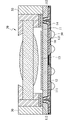
如图1所示,本实施例所提供的一种具有特定焦距的晶圆级影像感测器模块结构,其包括:一影像感测晶片10;一晶圆级透镜组20;以及一封装胶材30。As shown in FIG. 1, a wafer-level image sensor module structure with a specific focal length provided by this embodiment includes: an
其中,影像感测晶片10具有一第一表面11及一第二表面12,其分别为影像感测晶片10的上表面及下表面。第一表面11上设置有多个感光元件13,并且感光元件13是排列成阵列并设置于第一表面11上的感光区111中,进而用以感测光线。在第一表面11上设置有多个第一导电接点112,其是围绕设置于感光区111的外侧,并电性连接于感光元件13(通过影像感测晶片10内设置的电路结构)。Wherein, the
影像感测晶片10又包含至少一导电通道14,其穿透影像感测晶片10,并且导电通道14的一端电性连接于第一导电接点112,而另一端则电性连接于第二表面12上的多个植球焊垫121,以作为感光元件13与外界电性连接的通道。The
而在影像感测晶片10的第二表面12上可进一步布植焊球50,并电性连接于植球焊垫121,以在第二表面12上形成一球栅阵列51(请同时参阅图8所示)。焊球50不但电性连接于植球焊垫121,而且也通过植球焊垫121与导电通道14电性连接,因此可作为感光元件13与外界电性连接的介面。On the
接着,请继续参阅图1所示,晶圆级透镜组20,是对应设置于感光区111上方。其中,晶圆级透镜组20指的是以晶圆制造方式所制造的高准度透镜组,并且因在制造时已经经过精确地测试,所以晶圆级透镜组20具有一特定焦距,而且因晶圆级透镜组20为预先组立测试完成的模块,所以在本晶圆级影像感测器模块的制造过程无需再经过影像调焦的工序,故可以减少调焦设备的投资与调焦人力的成本。Next, please continue to refer to FIG. 1 , the wafer-
封装胶材30,设置于第一表面11上并包覆着晶圆级透镜组20的四周。其中,依封装方式的不同,封装胶材30可为一模塑封胶(mold compound)或一液态封胶(liquid compound)。又由于封装胶材30可以为不透光的材料,因此可利用不透光的封装胶材30避免光线由晶圆级透镜组20的侧边入射至影像感测器模块结构中。The
如图2至图4所示,上述的具有特定焦距的晶圆级影像感测器模块结构的制造方法包括下列步骤:提供一硅晶圆(S100);提供一透镜组晶圆(S200);根据不同品质分级筛选影像感测晶片及晶圆级透镜组(S300);依照品质分级筛选结果分配每一晶圆级透镜组设置于同等级的每一影像感测晶片上(S400);进行一封装工艺(S500);布植焊球(S600);以及切割硅晶圆,以形成多个影像感测器模块结构(S700)。As shown in FIGS. 2 to 4, the above-mentioned manufacturing method of the wafer-level image sensor module structure with a specific focal length includes the following steps: providing a silicon wafer (S100); providing a lens group wafer (S200); Screening image sensing chips and wafer-level lens groups according to different quality classifications (S300); assigning each wafer-level lens group to be arranged on each image sensing chip of the same level according to the quality classification screening results (S400); performing a packaging process (S500); implanting solder balls (S600); and dicing the silicon wafer to form a plurality of image sensor module structures (S700).
提供一硅晶圆(S100):如图5A所示,硅晶圆40可以为一硅导孔(Through-Silicon Vias,TSV)晶圆。硅导孔晶圆的剖视结构如图1所示,其借由在晶圆结构上形成导孔,并在导孔中设置导电通道14,以利用导电通道14与硅晶圆40的第一表面41(即影像感测晶片10的第一表面11)上的第一导电接点112电性连接,而且导电通道14也可延伸设置于第二表面42(即影像感测晶片10的第二表面12)。又可形成一再布线层(Re-distribution Layer)(图未示)于第二表面42,而再布线层可以与形成栅格阵列(Land Grid Array,LGA)形式的植球焊垫121电性连接,以借由再布线层布置在植球焊垫121间的间距。Providing a silicon wafer ( S100 ): as shown in FIG. 5A , the
硅晶圆40中包括多个影像感测晶片10,并且在每一影像感测晶片10的第一表面11(即为硅晶圆40的第一表面41)上皆具有一感光区111,而第一导电接点112则环绕设置于感光区111的外侧(请参阅图1所示)。The
提供一透镜组晶圆(S200):如图5B所示,透镜组晶圆60是以晶圆制造方式所制造的高准度透镜组,并且包括多个晶圆级透镜组20。而且因在制造过程晶圆级透镜组20已经过精确地测试,所以晶圆级透镜组20已具有经过测试的特定焦距,并且透镜组晶圆60在经过切割后可分为多个晶圆级透镜组20。Provide a lens group wafer ( S200 ): As shown in FIG. 5B , the
根据不同品质分级筛选影像感测晶片及晶圆级透镜组(S300):硅晶圆40中的每一影像感测晶片10都要先经过测试,以确定影像感测晶片10可正常运作并确认其品质。同样的,晶圆级透镜组20也需要经过测试,以检查晶圆级透镜组20的品质。因此,在测试检查影像感测晶片10及晶圆级透镜组20后,可依据不同品质分级筛选影像感测晶片10及晶圆级透镜组20,以将影像感测晶片10及晶圆级透镜组20进行分类。Classify and screen image sensor chips and wafer-level lens groups according to different qualities (S300): Each
依照品质分级筛选结果分配每一晶圆级透镜组设置于同等级的每一影像感测晶片上(S400):根据品质分级筛选结果,可将影像感测晶片10及晶圆级透镜组20至少大致区分为良好及较差两大类,因此如图5C所示,可将良好的晶圆级透镜组20分配设置于良好的影像感测晶片10上,而将相对较差的晶圆级透镜组20分配设置于相对较差的影像感测晶片10上,借此可以提高影像感测器模块结构产品的制造良率。Allocate each wafer-level lens group to be arranged on each image sensor chip of the same level according to the quality classification screening result (S400): according to the quality classification screening result, the
其中,每一晶圆级透镜组20是正对每一影像感测晶片10的感光区111(如图1所示),以使得光线可穿过晶圆级透镜组20中的透镜,并聚焦于影像感测晶片10的感光元件13。Wherein, each wafer-
进行一封装工艺(S500):可同时参阅图6C及图7C所示,借由封装工艺使封装胶材30设置于硅晶圆40的第一表面41上,并使封装胶材30包覆晶圆级透镜组20的四周,以封装硅晶圆40上的晶圆级透镜组20及影像感测晶片10。其中,封装工艺(S500)可为二种实施形态,分别叙述如下。Carry out an encapsulation process (S500): as shown in FIG. 6C and FIG. 7C at the same time, the
如图3所示,封装工艺(S500)的第一种实施形态包括下列步骤:设置一拦坝于第一表面的边缘,并形成一环状结构(S510);以及涂布封装胶材于拦坝内,且使封装胶材包覆晶圆级透镜组的四周(S511)。As shown in Figure 3, the first embodiment of the packaging process (S500) includes the following steps: setting a dam on the edge of the first surface, and forming a ring structure (S510); and coating the packaging adhesive on the dam inside the dam, and make the encapsulation material cover the periphery of the wafer-level lens group (S511).
设置一拦坝于第一表面的边缘,并形成一环状结构(S510):如图6A所示,在硅晶圆40第一表面41的边缘设置一拦坝43,以在硅晶圆40的外围形成一环状结构,进而使设置有晶圆级透镜组20的影像感测晶片10都在拦坝43所形成的环状结构中。Set a dam on the edge of the first surface, and form a ring structure (S510): as shown in FIG. The periphery of the dam forms a ring structure, so that the
涂布封装胶材于拦坝内,且使封装胶材包覆晶圆级透镜组的四周(S511):如图6B及图6C所示,利用点胶(dispensing)技术使封装胶材30涂布于第一表面41上,并使得封装胶材30填满拦坝43及晶圆级透镜组20之间,以使得封装胶材30包覆晶圆级透镜组20的四周,但不覆盖到晶圆级透镜组20的上缘,其中所使用的封装胶材30为液态封胶(liquidcompound)。Coating the packaging glue in the dam, and making the packaging glue wrap around the wafer-level lens group (S511): as shown in FIG. 6B and FIG. 6C, the
又如图4所示,封装工艺(S500)的第二种实施形态包括下列步骤:放置具有晶圆级透镜组的硅晶圆于一模具中(S520);注入封装胶材于模具的模穴中,以使封装胶材包覆晶圆级透镜组的四周(S521);以及转移成型并固化封装胶材(S522)。As shown in Figure 4, the second embodiment of the packaging process (S500) includes the following steps: placing a silicon wafer with a wafer-level lens group in a mold (S520); injecting the packaging adhesive into the mold cavity of the mold , so that the encapsulation material wraps around the wafer-level lens group (S521); and transfer molding and curing the encapsulation material (S522).
放置具有晶圆级透镜组的硅晶圆于一模具中(S520):如图7A所示,将已设置有晶圆级透镜组20的硅晶圆40放置于一模具70中。而模具70包括有一上模具71及一下模具72,其中上模具71的内表面是抵住晶圆级透镜组20的上缘,而下模具72用以承载硅晶圆40并抵住硅晶圆40的第二表面42。Place the silicon wafer with the wafer-level lens group in a mold ( S520 ): as shown in FIG. 7A , place the
又为了避免模造成型时,上模具71直接接触到晶圆级透镜组20的上缘而造成晶圆级透镜组20上缘溢胶,上模具71可包含利用真空吸附的一缓冲层73,并设置于晶圆级透镜组20与上模具71之间,用以抵住晶圆级透镜组20的上缘,进而防止晶圆级透镜组20上缘的溢胶现象。In addition, in order to prevent the
注入封装胶材于模具的模穴中,以使封装胶材包覆晶圆级透镜组的四周(S521):请参阅图7A所示,可将封装胶材30注入于模具70所形成的模穴中,并使得封装胶材30得以包覆晶圆级透镜组20的四周,但不覆盖到晶圆级透镜组20的上缘。Inject the encapsulant into the mold cavity of the mold so that the encapsulant covers the periphery of the wafer-level lens group (S521): as shown in FIG. 7A , the
转移成型并固化封装胶材(S522):请再同时参阅图7B及图7C所示,将封装胶材30注入模具70的模穴后,可借由模具70加压以使得封装胶材30转移成型后,再开模进行后烘烤(Post Mold Cure)工艺以固化封装胶材30。其中,所使用的封装胶材30为一模塑封胶(mold compound)。Transfer molding and curing the packaging material (S522): Please refer to FIG. 7B and FIG. 7C at the same time. After the
请再参阅图2所示,完成上述封装工艺(S500)后,可再进行布植焊球(S600);以及切割硅晶圆,以形成多个影像感测器模块结构(S700)。Please refer to FIG. 2 again. After the packaging process (S500) is completed, the solder balls can be planted (S600); and the silicon wafer can be cut to form multiple image sensor module structures (S700).
布植焊球(S600):如图8所示,在完成封装工艺后,可翻转硅晶圆40并在第二表面42上布植焊球50,并使焊球50布植于植球焊垫121上,并形成一球栅阵列51,借此使影像感测晶片10可经由第一导电接点112、导电通道14、植球焊垫121及焊球50与外部装置(如电路基板)进行电性连接。Implanting solder balls (S600): as shown in FIG. 8, after the packaging process is completed, the
切割硅晶圆,以形成多个影像感测器模块结构(S700):请同时参阅图9所示,可依照预设的切割线80切割硅晶圆40,借此形成多个影像感测器模块结构,而每个影像感测器模块结构则如图1所示。Dicing the silicon wafer to form a plurality of image sensor module structures (S700): please also refer to FIG. 9, the
借由本实施例的实施,可利用依品质分级筛选的机制,使同等级的晶圆级透镜组20和影像感测晶片10可相互组装,进而提高影像感测器模块结构产品的制造良率。再者,因可以选用不透光的封装胶材30,所以可以达到遮光的功效,因此无须再增加遮光罩或再增加涂布遮光材料的工艺即可避免因光线由晶圆级透镜组20侧边入射所造成的影像品质不良问题,例如眩光(Flare)问题。Through the implementation of this embodiment, the mechanism of grading and screening based on quality can be used to enable the wafer-
此外,因为是使用硅导孔工艺技术的硅晶圆40,所以不但可以免去如COB工艺中基板的设置,并可借此减少影像感测器模块结构整体的高度。而且因晶圆级透镜组20的组装结构在制造时已固定,并具有特定的焦距,所以也无须再经过调焦工艺,因此不但可以简化影像感测器模块结构的制造步骤,更可减少影像感测器模块的高度,以达到减少材料使用而达到降低成本的功效。In addition, because the
以上所述,仅是本发明的较佳实施例而已,并非对本发明作任何形式上的限制,虽然本发明已以较佳实施例揭露如上,然而并非用以限定本发明,任何熟悉本专业的技术人员,在不脱离本发明技术方案范围内,当可利用上述揭示的技术内容作出些许更动或修饰为等同变化的等效实施例,但凡是未脱离本发明技术方案内容,依据本发明的技术实质对以上实施例所作的任何简单修改、等同变化与修饰,均仍属于本发明技术方案的范围内。The above description is only a preferred embodiment of the present invention, and does not limit the present invention in any form. Although the present invention has been disclosed as above with preferred embodiments, it is not intended to limit the present invention. Anyone familiar with this field Those skilled in the art, without departing from the scope of the technical solution of the present invention, may use the technical content disclosed above to make some changes or modify them into equivalent embodiments with equivalent changes, but as long as they do not depart from the technical solution of the present invention, the Technical Essence Any simple modifications, equivalent changes and modifications made to the above embodiments still fall within the scope of the technical solution of the present invention.
Claims (14)
Priority Applications (1)
| Application Number | Priority Date | Filing Date | Title |
|---|---|---|---|
| CN201010188274XA CN102263113A (en) | 2010-05-24 | 2010-05-24 | Wafer-level image sensor module structure with specific focal length and manufacturing method thereof |
Applications Claiming Priority (1)
| Application Number | Priority Date | Filing Date | Title |
|---|---|---|---|
| CN201010188274XA CN102263113A (en) | 2010-05-24 | 2010-05-24 | Wafer-level image sensor module structure with specific focal length and manufacturing method thereof |
Publications (1)
| Publication Number | Publication Date |
|---|---|
| CN102263113A true CN102263113A (en) | 2011-11-30 |
Family
ID=45009681
Family Applications (1)
| Application Number | Title | Priority Date | Filing Date |
|---|---|---|---|
| CN201010188274XA Pending CN102263113A (en) | 2010-05-24 | 2010-05-24 | Wafer-level image sensor module structure with specific focal length and manufacturing method thereof |
Country Status (1)
| Country | Link |
|---|---|
| CN (1) | CN102263113A (en) |
Cited By (10)
| Publication number | Priority date | Publication date | Assignee | Title |
|---|---|---|---|---|
| CN103579259A (en) * | 2012-07-18 | 2014-02-12 | 宏翔光电股份有限公司 | Wafer-level imaging module structure |
| CN103715210A (en) * | 2012-10-09 | 2014-04-09 | 胜开科技股份有限公司 | Structure and manufacturing method of high-resolution camera module |
| CN103956369A (en) * | 2014-05-20 | 2014-07-30 | 苏州晶方半导体科技股份有限公司 | Image sensor module and forming method thereof |
| CN104347644A (en) * | 2013-07-25 | 2015-02-11 | 意法半导体研发(深圳)有限公司 | Image detector with lens component and correlation method |
| CN105244359A (en) * | 2015-10-28 | 2016-01-13 | 苏州晶方半导体科技股份有限公司 | Image sensing chip packaging structure and packaging method |
| CN105530410A (en) * | 2014-09-30 | 2016-04-27 | 豪威光电子科技(上海)有限公司 | Forming method of lens encapsulation module |
| CN105827910A (en) * | 2015-01-26 | 2016-08-03 | 全视技术有限公司 | Wafer-level lens packaging methods, and associated lens assemblies and camera modules |
| WO2017071426A1 (en) * | 2015-10-28 | 2017-05-04 | 苏州晶方半导体科技股份有限公司 | Image sensing chip packaging structure and packaging method |
| CN107682596A (en) * | 2016-08-01 | 2018-02-09 | 宁波舜宇光电信息有限公司 | Mold photosensory assembly and its jigsaw and preparation method |
| WO2022242050A1 (en) * | 2021-05-18 | 2022-11-24 | 苏州晶方半导体科技股份有限公司 | Packaging structure for image sensor chip |
Citations (4)
| Publication number | Priority date | Publication date | Assignee | Title |
|---|---|---|---|---|
| US20080038873A1 (en) * | 2006-08-10 | 2008-02-14 | Denso Corporation | Apparatus and method for manufacturing semiconductor device |
| US20090068798A1 (en) * | 2007-09-07 | 2009-03-12 | Micron Technology, Inc. | Imager die package and methods of packaging an imager die on a temporary carrier |
| US20090243051A1 (en) * | 2008-03-28 | 2009-10-01 | Micron Technology, Inc. | Integrated conductive shield for microelectronic device assemblies and associated methods |
| US20100006966A1 (en) * | 2008-07-10 | 2010-01-14 | Chia-Hsi Tsai | Method for making lens modules and lens module made thereby |
-
2010
- 2010-05-24 CN CN201010188274XA patent/CN102263113A/en active Pending
Patent Citations (4)
| Publication number | Priority date | Publication date | Assignee | Title |
|---|---|---|---|---|
| US20080038873A1 (en) * | 2006-08-10 | 2008-02-14 | Denso Corporation | Apparatus and method for manufacturing semiconductor device |
| US20090068798A1 (en) * | 2007-09-07 | 2009-03-12 | Micron Technology, Inc. | Imager die package and methods of packaging an imager die on a temporary carrier |
| US20090243051A1 (en) * | 2008-03-28 | 2009-10-01 | Micron Technology, Inc. | Integrated conductive shield for microelectronic device assemblies and associated methods |
| US20100006966A1 (en) * | 2008-07-10 | 2010-01-14 | Chia-Hsi Tsai | Method for making lens modules and lens module made thereby |
Cited By (16)
| Publication number | Priority date | Publication date | Assignee | Title |
|---|---|---|---|---|
| CN103579259A (en) * | 2012-07-18 | 2014-02-12 | 宏翔光电股份有限公司 | Wafer-level imaging module structure |
| CN103715210A (en) * | 2012-10-09 | 2014-04-09 | 胜开科技股份有限公司 | Structure and manufacturing method of high-resolution camera module |
| CN104347644B (en) * | 2013-07-25 | 2018-06-19 | 意法半导体研发(深圳)有限公司 | Visual detector and correlation technique with lens subassembly |
| CN104347644A (en) * | 2013-07-25 | 2015-02-11 | 意法半导体研发(深圳)有限公司 | Image detector with lens component and correlation method |
| CN103956369A (en) * | 2014-05-20 | 2014-07-30 | 苏州晶方半导体科技股份有限公司 | Image sensor module and forming method thereof |
| CN105530410A (en) * | 2014-09-30 | 2016-04-27 | 豪威光电子科技(上海)有限公司 | Forming method of lens encapsulation module |
| CN105530410B (en) * | 2014-09-30 | 2019-05-07 | 豪威光电子科技(上海)有限公司 | The forming method of camera lens encapsulated modules |
| CN105827910A (en) * | 2015-01-26 | 2016-08-03 | 全视技术有限公司 | Wafer-level lens packaging methods, and associated lens assemblies and camera modules |
| CN105244359A (en) * | 2015-10-28 | 2016-01-13 | 苏州晶方半导体科技股份有限公司 | Image sensing chip packaging structure and packaging method |
| TWI615958B (en) * | 2015-10-28 | 2018-02-21 | 蘇州晶方半導體科技股份有限公司 | Packaging structure and packaging method for image sensor chip |
| CN105244359B (en) * | 2015-10-28 | 2019-02-26 | 苏州晶方半导体科技股份有限公司 | Image sensing chip-packaging structure and packaging method |
| WO2017071426A1 (en) * | 2015-10-28 | 2017-05-04 | 苏州晶方半导体科技股份有限公司 | Image sensing chip packaging structure and packaging method |
| US10541262B2 (en) | 2015-10-28 | 2020-01-21 | China Wafer Level Csp Co., Ltd. | Image sensing chip packaging structure and packaging method |
| CN107682596A (en) * | 2016-08-01 | 2018-02-09 | 宁波舜宇光电信息有限公司 | Mold photosensory assembly and its jigsaw and preparation method |
| CN107682596B (en) * | 2016-08-01 | 2021-03-09 | 宁波舜宇光电信息有限公司 | Molded photosensitive component, jointed board thereof and manufacturing method |
| WO2022242050A1 (en) * | 2021-05-18 | 2022-11-24 | 苏州晶方半导体科技股份有限公司 | Packaging structure for image sensor chip |
Similar Documents
| Publication | Publication Date | Title |
|---|---|---|
| TWI449162B (en) | Method for manufacturing wafer level image sensor module with specific focal length | |
| CN102263113A (en) | Wafer-level image sensor module structure with specific focal length and manufacturing method thereof | |
| US8563350B2 (en) | Wafer level image sensor packaging structure and manufacturing method for the same | |
| TWI414061B (en) | Wafer level image sensor module manufacturing method with package structure | |
| TWI414060B (en) | Mold-free type of focus-distance image sensor assembly structure and manufacturing method thereof | |
| JP4503677B2 (en) | Semiconductor package with upper and lower substrate surfaces exposed | |
| TWI398949B (en) | Image-forming image sensor package structure manufacturing method and package structure | |
| CN104078479B (en) | The wafer-level packaging method of imageing sensor and image sensor package structure | |
| US8110884B2 (en) | Methods of packaging imager devices and optics modules, and resulting assemblies | |
| US12278248B2 (en) | Image sensor package and method of fabricating the same | |
| CN101315939A (en) | Chip-size image sensor with die receiving opening and method of making the same | |
| US9419047B2 (en) | Image sensor device with aligned IR filter and dielectric layer and related methods | |
| JP2012094882A (en) | Manufacturing method for wafer-level image sensor module | |
| CN103996684A (en) | Image sensor structure and packaging method thereof | |
| CN107958881A (en) | A kind of CIS device encapsulation structures and method for packing | |
| CN102403323B (en) | Wafer-level image sensor assembly structure and manufacturing method thereof | |
| CN105070732A (en) | High-pixel image sensor packaging structure and manufacturing method thereof | |
| US8703519B1 (en) | Structure and manufacturing method for high resolution camera module | |
| CN111415954A (en) | Packaging structure and method of back-illuminated image sensor chip | |
| TWI476876B (en) | Window image module structure | |
| US20240072084A1 (en) | Image sensor package and method of fabricating the same | |
| CN115274719A (en) | Image sensor and method of making the same | |
| TW201401495A (en) | Wafer level camera module structure |
Legal Events
| Date | Code | Title | Description |
|---|---|---|---|
| C06 | Publication | ||
| PB01 | Publication | ||
| C10 | Entry into substantive examination | ||
| SE01 | Entry into force of request for substantive examination | ||
| C02 | Deemed withdrawal of patent application after publication (patent law 2001) | ||
| WD01 | Invention patent application deemed withdrawn after publication |
Application publication date: 20111130 |