CN102255015A - Method for emitting circularly polarized light using LED (light-emitting diode) chip, and product and preparation method thereof - Google Patents
Method for emitting circularly polarized light using LED (light-emitting diode) chip, and product and preparation method thereof Download PDFInfo
- Publication number
- CN102255015A CN102255015A CN2011101901020A CN201110190102A CN102255015A CN 102255015 A CN102255015 A CN 102255015A CN 2011101901020 A CN2011101901020 A CN 2011101901020A CN 201110190102 A CN201110190102 A CN 201110190102A CN 102255015 A CN102255015 A CN 102255015A
- Authority
- CN
- China
- Prior art keywords
- layer
- light
- emitting
- type
- led chip
- Prior art date
- Legal status (The legal status is an assumption and is not a legal conclusion. Google has not performed a legal analysis and makes no representation as to the accuracy of the status listed.)
- Granted
Links
- 238000000034 method Methods 0.000 title claims abstract description 44
- 238000002360 preparation method Methods 0.000 title claims abstract description 11
- 238000004519 manufacturing process Methods 0.000 title description 2
- 239000004065 semiconductor Substances 0.000 claims abstract description 72
- 230000005291 magnetic effect Effects 0.000 claims abstract description 64
- 239000000758 substrate Substances 0.000 claims abstract description 52
- 239000000463 material Substances 0.000 claims abstract description 25
- 239000000969 carrier Substances 0.000 claims abstract description 15
- 229910052723 transition metal Inorganic materials 0.000 claims abstract description 14
- 238000002347 injection Methods 0.000 claims abstract description 11
- 239000007924 injection Substances 0.000 claims abstract description 11
- 150000003624 transition metals Chemical class 0.000 claims abstract description 10
- 230000006798 recombination Effects 0.000 claims abstract description 8
- 238000005215 recombination Methods 0.000 claims abstract description 8
- 239000010410 layer Substances 0.000 claims description 253
- 238000005530 etching Methods 0.000 claims description 26
- 238000000206 photolithography Methods 0.000 claims description 17
- 238000001451 molecular beam epitaxy Methods 0.000 claims description 12
- 150000001875 compounds Chemical class 0.000 claims description 8
- 229910052751 metal Inorganic materials 0.000 claims description 8
- 239000002184 metal Substances 0.000 claims description 8
- 239000000047 product Substances 0.000 claims description 7
- 239000011241 protective layer Substances 0.000 claims description 7
- 229910052733 gallium Inorganic materials 0.000 claims description 5
- 229910052738 indium Inorganic materials 0.000 claims description 5
- 238000002161 passivation Methods 0.000 claims description 5
- 239000000126 substance Substances 0.000 claims description 5
- 230000032258 transport Effects 0.000 claims description 5
- 238000005229 chemical vapour deposition Methods 0.000 claims description 4
- 229910052742 iron Inorganic materials 0.000 claims description 4
- 239000002131 composite material Substances 0.000 claims description 3
- 238000000151 deposition Methods 0.000 claims description 3
- 230000008021 deposition Effects 0.000 claims description 3
- 229910052748 manganese Inorganic materials 0.000 claims description 3
- 229910052725 zinc Inorganic materials 0.000 claims description 3
- 229910052787 antimony Inorganic materials 0.000 claims description 2
- 229910052804 chromium Inorganic materials 0.000 claims description 2
- 239000002070 nanowire Substances 0.000 claims description 2
- 229910052759 nickel Inorganic materials 0.000 claims description 2
- 230000001681 protective effect Effects 0.000 claims description 2
- 239000002096 quantum dot Substances 0.000 claims description 2
- 239000011265 semifinished product Substances 0.000 claims description 2
- 239000003086 colorant Substances 0.000 abstract description 4
- 239000000203 mixture Substances 0.000 abstract description 4
- 230000005389 magnetism Effects 0.000 abstract 1
- 229910002601 GaN Inorganic materials 0.000 description 35
- 229920002120 photoresistant polymer Polymers 0.000 description 24
- 239000010408 film Substances 0.000 description 17
- 238000004140 cleaning Methods 0.000 description 15
- 239000000243 solution Substances 0.000 description 12
- 238000005516 engineering process Methods 0.000 description 10
- 238000002488 metal-organic chemical vapour deposition Methods 0.000 description 10
- KRHYYFGTRYWZRS-UHFFFAOYSA-N Fluorane Chemical compound F KRHYYFGTRYWZRS-UHFFFAOYSA-N 0.000 description 9
- 229910004298 SiO 2 Inorganic materials 0.000 description 9
- 238000001020 plasma etching Methods 0.000 description 9
- 239000013078 crystal Substances 0.000 description 8
- 239000010409 thin film Substances 0.000 description 7
- VEXZGXHMUGYJMC-UHFFFAOYSA-N Hydrochloric acid Chemical compound Cl VEXZGXHMUGYJMC-UHFFFAOYSA-N 0.000 description 6
- 229910052594 sapphire Inorganic materials 0.000 description 6
- 239000010980 sapphire Substances 0.000 description 6
- 238000000137 annealing Methods 0.000 description 5
- GYHNNYVSQQEPJS-UHFFFAOYSA-N Gallium Chemical group [Ga] GYHNNYVSQQEPJS-UHFFFAOYSA-N 0.000 description 3
- JMASRVWKEDWRBT-UHFFFAOYSA-N Gallium nitride Chemical compound [Ga]#N JMASRVWKEDWRBT-UHFFFAOYSA-N 0.000 description 3
- NWAIGJYBQQYSPW-UHFFFAOYSA-N azanylidyneindigane Chemical compound [In]#N NWAIGJYBQQYSPW-UHFFFAOYSA-N 0.000 description 3
- 238000005520 cutting process Methods 0.000 description 3
- 238000000227 grinding Methods 0.000 description 3
- 239000012535 impurity Substances 0.000 description 3
- APFVFJFRJDLVQX-UHFFFAOYSA-N indium atom Chemical compound [In] APFVFJFRJDLVQX-UHFFFAOYSA-N 0.000 description 3
- 238000001755 magnetron sputter deposition Methods 0.000 description 3
- 229910021645 metal ion Inorganic materials 0.000 description 3
- 238000005121 nitriding Methods 0.000 description 3
- 230000005693 optoelectronics Effects 0.000 description 3
- 230000010287 polarization Effects 0.000 description 3
- 238000012805 post-processing Methods 0.000 description 3
- 238000004544 sputter deposition Methods 0.000 description 3
- 238000004506 ultrasonic cleaning Methods 0.000 description 3
- OKTJSMMVPCPJKN-UHFFFAOYSA-N Carbon Chemical compound [C] OKTJSMMVPCPJKN-UHFFFAOYSA-N 0.000 description 2
- 229910002804 graphite Inorganic materials 0.000 description 2
- 239000010439 graphite Substances 0.000 description 2
- 150000002500 ions Chemical class 0.000 description 2
- NJPPVKZQTLUDBO-UHFFFAOYSA-N novaluron Chemical compound C1=C(Cl)C(OC(F)(F)C(OC(F)(F)F)F)=CC=C1NC(=O)NC(=O)C1=C(F)C=CC=C1F NJPPVKZQTLUDBO-UHFFFAOYSA-N 0.000 description 2
- 150000002902 organometallic compounds Chemical class 0.000 description 2
- 239000012808 vapor phase Substances 0.000 description 2
- 230000009286 beneficial effect Effects 0.000 description 1
- 239000002800 charge carrier Substances 0.000 description 1
- 238000006243 chemical reaction Methods 0.000 description 1
- 230000007547 defect Effects 0.000 description 1
- 238000010586 diagram Methods 0.000 description 1
- 239000002019 doping agent Substances 0.000 description 1
- 230000000694 effects Effects 0.000 description 1
- 230000002349 favourable effect Effects 0.000 description 1
- 230000005294 ferromagnetic effect Effects 0.000 description 1
- 229910021478 group 5 element Inorganic materials 0.000 description 1
- 229910021476 group 6 element Inorganic materials 0.000 description 1
- 150000004678 hydrides Chemical class 0.000 description 1
- 230000006698 induction Effects 0.000 description 1
- 239000007788 liquid Substances 0.000 description 1
- 239000004973 liquid crystal related substance Substances 0.000 description 1
- 230000007774 longterm Effects 0.000 description 1
- 238000004020 luminiscence type Methods 0.000 description 1
- 239000000696 magnetic material Substances 0.000 description 1
- 239000006249 magnetic particle Substances 0.000 description 1
- 230000014759 maintenance of location Effects 0.000 description 1
- 150000002739 metals Chemical class 0.000 description 1
- 150000004767 nitrides Chemical class 0.000 description 1
- 150000002894 organic compounds Chemical class 0.000 description 1
- 239000010453 quartz Substances 0.000 description 1
- 230000005855 radiation Effects 0.000 description 1
- VYPSYNLAJGMNEJ-UHFFFAOYSA-N silicon dioxide Inorganic materials O=[Si]=O VYPSYNLAJGMNEJ-UHFFFAOYSA-N 0.000 description 1
- 239000002356 single layer Substances 0.000 description 1
- 239000006104 solid solution Substances 0.000 description 1
- 229910001220 stainless steel Inorganic materials 0.000 description 1
- 239000010935 stainless steel Substances 0.000 description 1
- 238000005979 thermal decomposition reaction Methods 0.000 description 1
- 230000007704 transition Effects 0.000 description 1
- 238000007738 vacuum evaporation Methods 0.000 description 1
- 238000000927 vapour-phase epitaxy Methods 0.000 description 1
Images


Landscapes
- Led Devices (AREA)
Abstract
本发明公开了一种利用LED芯片发射圆偏振光的方法及产品及其制备方法,在LED芯片顶层的n型层或p型层中加入过渡金属,使顶层的n型层或p型层具有磁性,为LED芯片的发光层提供自旋极化的载流子注入,再将其输运到发光层与衬底基片一侧的p型层或n型层中提供的未自旋极化的载流子辐射复合,使LED芯片的发光层发射出圆偏振光。本发明采用在LED芯片pn结半导体层材料中加入过渡金属引入磁性的方法,使pn结半导体层能为发光层提供极化的自旋载流子注入,以实现LED芯片发出圆偏振光的目的。并且,还可以通过调整所述LED芯片的发光层的结构及材料组分,以获得不同颜色的圆偏振光。
The invention discloses a method for emitting circularly polarized light by using an LED chip, a product and a preparation method thereof. A transition metal is added to the n-type layer or the p-type layer of the top layer of the LED chip, so that the n-type layer or the p-type layer of the top layer has Magnetic, providing spin-polarized carrier injection for the light-emitting layer of the LED chip, and then transporting it to the non-spin-polarized layer provided in the p-type layer or n-type layer on the side of the light-emitting layer and the substrate The radiative recombination of the carriers makes the light-emitting layer of the LED chip emit circularly polarized light. The invention adopts the method of adding transition metal into the pn junction semiconductor layer material of the LED chip to introduce magnetism, so that the pn junction semiconductor layer can provide polarized spin carrier injection for the light emitting layer, so as to realize the purpose of the LED chip emitting circularly polarized light . Moreover, circularly polarized light of different colors can also be obtained by adjusting the structure and material composition of the light emitting layer of the LED chip.
Description
技术领域 technical field
本发明涉及一种发射圆偏振光的LED芯片及其制备方法,尤其是一种发射圆偏振光的GaN基LED芯片及其制备方法。 The invention relates to an LED chip emitting circularly polarized light and a preparation method thereof, in particular to a GaN-based LED chip emitting circularly polarized light and a preparation method thereof.
背景技术 Background technique
光电子技术是21世纪的尖端技术,LED(light emitting diode)是光电子产业中最重要的光电子材料和组件之一。LED是一种电致发光器件,它通过正向偏置的PN结中电子与空穴的辐射复合发光。在传统LED器件中,电子只被看着电荷的载体,自旋这一概念常常被人们忽略。 Optoelectronic technology is a cutting-edge technology in the 21st century, and LED (light emitting diode) is one of the most important optoelectronic materials and components in the optoelectronic industry. LED is an electroluminescent device that emits light through the radiative recombination of electrons and holes in a forward-biased PN junction. In traditional LED devices, electrons are only regarded as charge carriers, and the concept of spin is often ignored by people.
圆偏振光最为接近自然光,适合于人眼长期观看。因此,现实应用中常用偏振片来产生偏振光。但是,使用偏振片来产生偏振光将导致光的大量损失。例如,作为液晶显示器的LED背光源,当其光通过下层偏振片时,光的浪费已达50%。 Circularly polarized light is the closest to natural light and is suitable for long-term viewing by the human eye. Therefore, polarizers are often used in practical applications to generate polarized light. However, using a polarizer to create polarized light will result in a large loss of light. For example, as an LED backlight for a liquid crystal display, when the light passes through the underlying polarizer, 50% of the light is wasted.
发明内容 Contents of the invention
本发明的目的是:提供一种利用LED芯片发射圆偏振光的方法及产品及其制备方法,该LED芯片能够直接发射出圆偏振光,可以克服利用偏振片产生偏振光时导致大量光被损失掉的不足。 The purpose of the present invention is to provide a method for emitting circularly polarized light by using an LED chip, a product and a preparation method thereof. The LED chip can directly emit circularly polarized light, which can overcome the loss of a large amount of light caused by using a polarizer to generate polarized light. Not enough drops.
本发明是这样实现的:利用LED芯片发射圆偏振光的方法,在LED芯片顶层的n型层或p型层中加入过渡金属,使顶层的n型层或p型层具有磁性,为LED芯片的发光层提供自旋极化的载流子注入,再将其输运到发光层与衬底基片一侧的p型层或n型层中提供的未自旋极化的载流子辐射复合,发射出圆偏振光;或者在发光层两侧的n型层及p型层中均加入过渡金属,使n型层及p型层均具有磁性,n型层及p型层同时注入自旋载流子,输运到发光层辐射复合,使LED芯片的发光层发射出圆偏振光。其中,当p区和n区同时提供自旋注入时,自旋方向相反的电子或空穴复合发射荧光,自旋方向相同的电子或空穴复合发射磷光。 The present invention is realized in the following way: by using the method of emitting circularly polarized light from the LED chip, a transition metal is added to the n-type layer or the p-type layer of the top layer of the LED chip, so that the n-type layer or the p-type layer of the top layer is magnetic, and the LED chip is The light-emitting layer provides spin-polarized carrier injection, and then transports it to the p-type layer or n-type layer on the side of the light-emitting layer and the substrate substrate to provide non-spin-polarized carrier radiation compound to emit circularly polarized light; or transition metals are added to both the n-type layer and the p-type layer on both sides of the light-emitting layer, so that both the n-type layer and the p-type layer are magnetic, and the n-type layer and the p-type layer are simultaneously injected into the self- The spin carriers are transported to the light-emitting layer for radiative recombination, so that the light-emitting layer of the LED chip emits circularly polarized light. Wherein, when the p region and the n region provide spin injection at the same time, electrons or holes with opposite spin directions recombine to emit fluorescence, and electrons or holes with the same spin direction recombine to emit phosphorescence.
所述的过渡金属为Mn、Co、Fe、Cr、Ni或Sb等。 The transition metal is Mn, Co, Fe, Cr, Ni or Sb and the like.
发射圆偏振光的LED芯片,包括衬底基片,衬底基片上的缓冲层,在缓冲层上的非磁性或磁性的半导体底层,在半导体底层上的发光层,在发光层上的磁性半导体顶层,在磁性半导体顶层上的透明电极层;在半导体底层及透明电极层上分别连接的底层电极及顶层电极,以及外部的露出底层电极及顶层电极顶面的钝化保护层。 LED chips that emit circularly polarized light, including a substrate, a buffer layer on the substrate, a non-magnetic or magnetic semiconductor bottom layer on the buffer layer, a light-emitting layer on the semiconductor bottom layer, and a magnetic semiconductor on the light-emitting layer The top layer is a transparent electrode layer on the top layer of the magnetic semiconductor; the bottom electrode and the top electrode are respectively connected to the semiconductor bottom layer and the transparent electrode layer, and an external passivation protection layer exposing the top surface of the bottom electrode and the top electrode.
发光层为发光层、量子阱、衬底图形化阵列生长的发光层、量子点发光层、纳米线发光层等中的一种或几种的复合结构。通过调整LED芯片的发光层结构及材料组分,可以发射出不同颜色圆偏振光;其中发光层、量子阱的层数可以为单层或多层,其层数根据所需要发光的颜色进行选择。 The light-emitting layer is one or a composite structure of light-emitting layer, quantum well, light-emitting layer grown in substrate patterned array, quantum dot light-emitting layer, nanowire light-emitting layer and the like. By adjusting the light-emitting layer structure and material composition of the LED chip, different colors of circularly polarized light can be emitted; the number of layers of the light-emitting layer and quantum well can be single layer or multi-layer, and the number of layers can be selected according to the required color of light emission. .
发光层的材料为至少含In或Ga的化合物半导体材料。 The material of the light emitting layer is a compound semiconductor material containing at least In or Ga.
在n型层或p型层中加入补偿元素。 Add compensation elements in n-type layer or p-type layer.
n型侧补偿元素为Si,p型侧补偿元素为Mg或Zn等。 The n-type side compensation element is Si, and the p-type side compensation element is Mg or Zn.
发射圆偏振光的LED芯片的制备方法,在衬底基片上生长缓冲层;在缓冲层上生长非磁性或磁性的半导体底层;在半导体底层上生长发光层;在发光层上生长磁性半导体顶层;在磁性半导体顶层的上沉积透明导电薄膜,并进行光刻和刻蚀;在半导体底层及透明导电薄膜上溅射出金属电极层,并进行光刻和刻蚀,得到底层电极及顶层电极;最后在半成品的外表面沉积出钝化保护薄膜,并进行光刻和刻蚀,同时露出底层电极及顶层电极的顶面,即得到成品。 A method for preparing an LED chip that emits circularly polarized light: growing a buffer layer on a substrate; growing a non-magnetic or magnetic semiconductor bottom layer on the buffer layer; growing a light-emitting layer on the semiconductor bottom layer; growing a magnetic semiconductor top layer on the light-emitting layer; Deposit a transparent conductive film on the top layer of the magnetic semiconductor, and perform photolithography and etching; sputter a metal electrode layer on the bottom layer of the semiconductor and the transparent conductive film, and perform photolithography and etching to obtain the bottom electrode and the top electrode; finally A passivation protective film is deposited on the outer surface of the semi-finished product, and photolithography and etching are performed to expose the bottom electrode and the top surface of the top electrode at the same time to obtain the finished product.
在衬底基片上制备缓冲层之前,先将衬底基片在1000~1200℃下烘烤18~22min,然后在500~1000℃下对衬底基片进行60~150s的氮化处理;在将经过处理的衬底基片上制备缓冲层。 Before preparing the buffer layer on the substrate, the substrate is first baked at 1000-1200°C for 18-22 minutes, and then the substrate is nitrided at 500-1000°C for 60-150s; Prepare the buffer layer on the treated substrate substrate.
缓冲层、半导体底层、发光层的制备采用金属有机化合物化学气相沉积法,半导体磁性层可以采用金属有机化合物化学气相沉积法或分子束外延法沉积。 The buffer layer, the semiconductor bottom layer, and the luminescent layer are prepared by metal organic compound chemical vapor deposition, and the semiconductor magnetic layer can be deposited by metal organic compound chemical vapor deposition or molecular beam epitaxy.
所述的磁性的半导体底层或磁性半导体顶层是在半导体材料中加入2~7%摩尔百分比的过渡金属元素,经过沉积得到的n型层或p型层,半导体底层与磁性半导体顶层的层形相反。加入过渡金属元素后,使n型层成稀磁半导体层,以形成载流子的自旋方向有序排列,而不是很关注掺入磁性粒子的量。过渡金属元素的加入量与具体加入的元素有关,在2~7%摩尔百分比的范围内选择比较合适;芯片的几何形状、金属电极的几何形状与位置可以按需要调整和改变。 The magnetic semiconductor bottom layer or the magnetic semiconductor top layer is an n-type layer or a p-type layer obtained by adding 2 to 7 mole percent transition metal elements into the semiconductor material, and the layer shape of the semiconductor bottom layer is opposite to that of the magnetic semiconductor top layer. . After adding transition metal elements, make the n-type layer into a dilute magnetic semiconductor layer to form an orderly arrangement of the spin direction of the carriers, rather than paying much attention to the amount of doped magnetic particles. The amount of transition metal elements added is related to the specific elements added, and it is more appropriate to choose within the range of 2-7% mole percent; the geometric shape of the chip, the geometric shape and position of the metal electrode can be adjusted and changed as required.
在自旋电子学领域,电子或空穴的自旋极化指的是作为载流子的电子或空穴会朝相反的方向自旋,分别称为上自旋和下自旋。例如,在费米能级处,铁磁金属中的电子是100%的下自旋极化。如果用磁性材料将传统LED的电子或空穴极化,为传统LED芯片提供自旋极化的电子或空穴注入,就能够将材料的磁性功能与LED的发光功能结合,得到发射圆偏振光的LED。在半导体化合物材料中掺入少量的过渡金属元素可以形成一种磁性化合物半导体。其晶体结构与化学键结最能与现有电子元件中半导体材料相匹配,在居里温度以下其能带的基曼分裂(Zeeman splitting)可以产生大的自旋偏极化,因此可以用作“为传统LED提供自旋极化”的载流子源。例如掺锰的Ga1-xMnxN薄膜,掺入的Mn离子取代部分的Ga离子,除了提供Mn本身的磁矩外,还提供自旋空穴(针对p型Ga1-xMnxN薄膜),因而非常适合于传统氮化镓基LED载流子自旋极化需求。 In the field of spintronics, the spin polarization of electrons or holes means that the electrons or holes as carriers will spin in opposite directions, which are called up-spin and down-spin, respectively. For example, at the Fermi level, electrons in ferromagnetic metals are 100% down-spin polarized. If magnetic materials are used to polarize the electrons or holes of traditional LEDs to provide spin-polarized electrons or holes for traditional LED chip injection, the magnetic function of the material can be combined with the light-emitting function of the LED to obtain circularly polarized light emission. LEDs. Doping a small amount of transition metal elements in semiconductor compound materials can form a magnetic compound semiconductor. Its crystal structure and chemical bonding can best match the semiconductor materials in existing electronic components. The Kiman splitting (Zeeman splitting) of its energy band below the Curie temperature can produce large spin polarization, so it can be used as " Provides "spin-polarized" carrier sources for conventional LEDs. For example, manganese-doped Ga 1-x Mn x N thin films, the doped Mn ions replace part of the Ga ions, in addition to providing the magnetic moment of Mn itself, it also provides spin holes (for p-type Ga 1-x Mn x N Thin film), so it is very suitable for the carrier spin polarization requirements of traditional GaN-based LEDs.
引入自旋载流子后的LED发射的是圆偏振光。若是直接发射圆偏振光的LED作为LCD背光源,如果能够利用光选择定则,通过外加磁场调制其圆偏振光为线偏振光,则不再需要下偏振片,从而解决一些相应技术问题。无论在通用照明领域,还是在诸如背光源、汽车前灯、显示屏、景观照明、指示标牌、特种照明等领域,圆偏振光的LED都具有无限的应用潜能。 The LED after the introduction of spin carriers emits circularly polarized light. If the LED that directly emits circularly polarized light is used as the LCD backlight, if the light selection rule can be used to modulate the circularly polarized light into linearly polarized light through an external magnetic field, the lower polarizer is no longer needed, thereby solving some corresponding technical problems. Whether in the field of general lighting, or in fields such as backlight, automotive headlights, display screens, landscape lighting, signage, special lighting, etc., circularly polarized LEDs have unlimited application potential.
引入自旋载流子后的LED,还涉及到另一个至关重要的问题是自旋载流子(电子或空穴)输运问题,即不考虑磁性层与发光层界面缺陷等各种工艺因素时,载流子极化自旋注入后的寿命问题或能否输运到发光层的问题。极化的自旋电子或空穴,其自旋保持(弛豫)时间比普通电子或空穴长,即具有更长的寿命和较远的输运距离,这为更多的载流子到达发光层复合发光提供了有利条件。这就表明,在合理的工艺条件下,施加同等的电流时,经由磁性层注入到LED发光层进行辐射复合发光的电子或空穴可以比传统LED多。 The LED after the introduction of spin carriers also involves another crucial issue is the transport of spin carriers (electrons or holes), that is, various processes such as interface defects between the magnetic layer and the light-emitting layer are not considered. Factors, the life of the carrier polarized spin injection or the problem of whether it can be transported to the light-emitting layer. Polarized spin electrons or holes have a longer spin retention (relaxation) time than ordinary electrons or holes, that is, have longer lifetimes and longer transport distances, which allow more carriers to reach The composite light emission of the light emitting layer provides favorable conditions. This shows that, under reasonable process conditions, when the same current is applied, more electrons or holes can be injected into the LED light-emitting layer through the magnetic layer for radiative recombination and light emission than traditional LEDs.
引入自旋载流子后的LED,还有一个重要问题,那就是制备问题,也就是是否能与现有半导体工艺兼容的问题。目前,除MOCVD法外,MBE法能在低温下得到居里温度达到或高于室温的高质量的氮化物稀磁性半导体薄膜。所得薄膜材料具有大的直接能隙,可以放出短波长的蓝光或紫外光,还具有高热导率、好的化学惰性、适合于高温条件操作等特点,并且,可以成功掺杂为n型或p型,且适合于异质结构,能与现有半导体工艺相兼容。这表明,过渡金属掺杂的磁性化合物半导体薄膜已能尽快推广到传统LED芯片现有工艺中。 There is another important issue for the LED after the introduction of spin carriers, that is, the issue of preparation, that is, whether it can be compatible with the existing semiconductor process. At present, in addition to the MOCVD method, the MBE method can obtain a high-quality nitride dilute magnetic semiconductor film at a low temperature with a Curie temperature at or above room temperature. The obtained thin film material has a large direct energy gap, can emit short-wavelength blue light or ultraviolet light, and also has the characteristics of high thermal conductivity, good chemical inertness, suitable for high temperature operation, etc., and can be successfully doped as n-type or p type, and is suitable for heterostructures, and is compatible with existing semiconductor processes. This shows that the transition metal-doped magnetic compound semiconductor film can be extended to the existing process of traditional LED chips as soon as possible.
MOCVD是金属有机化合物化学气相淀积(Metal-organic Chemical Vapor Deposition)的英文缩写。MOCVD是在气相外延生长(VPE)的基础上发展起来的一种新型气相外延生长技术。它以Ⅲ族、Ⅱ族元素的有机化合物和V、Ⅵ族元素的氢化物等作为晶体生长源材料,以热分解反应方式在衬底上进行气相外延,生长各种Ⅲ-V族、Ⅱ-Ⅵ族化合物半导体以及它们的多元固溶体的薄层单晶材料。通常MOCVD系统中的晶体生长都是在常压或低压(10-100Torr)下通H2的冷壁石英(不锈钢)反应室中进行,衬底温度为500-1200℃,用射频感应加热石墨基座(衬底基片在石墨基座上方),H2通过温度可控的液体源鼓泡携带金属有机物到生长区。 MOCVD is the English abbreviation of Metal-organic Chemical Vapor Deposition. MOCVD is a new type of vapor phase epitaxial growth technology developed on the basis of vapor phase epitaxial growth (VPE). It uses organic compounds of group III and group II elements and hydrides of group V and group VI elements as crystal growth source materials, and performs vapor phase epitaxy on the substrate in a thermal decomposition reaction mode to grow various group III-V, II- Thin-layer single-crystal materials of Group VI compound semiconductors and their multiple solid solutions. Usually, the crystal growth in MOCVD system is carried out in the cold-walled quartz (stainless steel) reaction chamber with H2 flowing under normal pressure or low pressure (10-100Torr), the substrate temperature is 500-1200℃, and the graphite substrate is heated by radio frequency induction. pedestal (the substrate substrate is above the graphite pedestal), H2 is bubbled through a temperature-controlled liquid source to carry metal organics to the growth zone.
MBE是分子束外延(Molecular Beam Epitaxy)的英文缩写。MBE是一种新的晶体生长技术,其方法是将半导体衬底放置在超高真空腔体中,和将需要生长的单晶物质按元素的不同分别放在喷射炉中(也在腔体内)。由分别加热到相应温度的各元素喷射出的分子流能在上述衬底上生长出极薄的(可薄至单原子层水平)单晶体和几种物质交替的超晶格结构。分子束外延主要研究的是不同结构或不同材料的晶体和超晶格的生长。该法生长温度低,能严格控制外延层的层厚组分和掺杂浓度,但系统复杂,生长速度慢,生长面积也受到一定限制。 MBE is the abbreviation of Molecular Beam Epitaxy. MBE is a new crystal growth technology. The method is to place the semiconductor substrate in an ultra-high vacuum chamber, and place the single crystal material to be grown in the jet furnace (also in the chamber) according to the different elements. . The molecular flow ejected by each element heated to the corresponding temperature can grow an extremely thin (can be as thin as a single atomic layer level) single crystal and a superlattice structure in which several substances alternate on the above substrate. Molecular beam epitaxy mainly studies the growth of crystals and superlattices of different structures or materials. The growth temperature of this method is low, and the layer thickness composition and doping concentration of the epitaxial layer can be strictly controlled, but the system is complex, the growth rate is slow, and the growth area is also limited to a certain extent. the
分子束外延是50年代用真空蒸发技术制备半导体薄膜材料发展而来的。随着超高真空技术的发展而日趋完善,由于分子束外延技术的发展开拓了一系列崭新的超晶格器件,扩展了半导体科学的新领域,进一步说明了半导体材料的发展对半导体物理和半导体器件的影响。分子束外延的优点就是能够制备超薄层的半导体材料;外延材料表面形貌好,而且面积较大均匀性较好;可以制成不同掺杂剂或不同成份的多层结构;外延生长的温度较低,有利于提高外延层的纯度和完整性;利用各种元素的粘附系数的差别,可制成化学配比较好的化合物半导体薄膜。 Molecular beam epitaxy was developed in the 1950s by using vacuum evaporation technology to prepare semiconductor thin film materials. With the development of ultra-high vacuum technology, it is becoming more and more perfect. Due to the development of molecular beam epitaxy technology, a series of new superlattice devices have been opened up, which has expanded the new field of semiconductor science, and further explained the development of semiconductor materials. Semiconductor physics and semiconductor device impact. The advantage of molecular beam epitaxy is that it can prepare ultra-thin semiconductor materials; the surface morphology of epitaxial materials is good, and the area is larger and the uniformity is better; it can be made into multi-layer structures with different dopants or different components; the temperature of epitaxial growth Low, it is beneficial to improve the purity and integrity of the epitaxial layer; using the difference in the adhesion coefficient of various elements, it can be made into a compound semiconductor film with a relatively good chemical ratio.
由于采用了上述的技术方案,与现有技术相比,本发明采用在LED芯片pn结半导体层的材料中加入过渡金属的方法,使半导体层能为发光层提供极化的自旋载流子注入,这些极化的空穴或电子输运到发光层后与另一侧提供的未极化或极化的电子或空穴辐射复合,以实现LED芯片发出圆偏振光的目的。并且,还可以通过调整所述LED芯片的发光层的结构及材料组分,以获得不同颜色的圆偏振光。本发明的方法简单,容易实施,产品的质量稳定性好,适用范围广,使用效果好。 Due to the adoption of the above-mentioned technical scheme, compared with the prior art, the present invention adopts the method of adding transition metal into the material of the pn junction semiconductor layer of the LED chip, so that the semiconductor layer can provide polarized spin carriers for the light-emitting layer. Injection, these polarized holes or electrons are transported to the light-emitting layer and recombine with the unpolarized or polarized electrons or holes provided by the other side to achieve the purpose of emitting circularly polarized light from the LED chip. Moreover, circularly polarized light of different colors can also be obtained by adjusting the structure and material composition of the light emitting layer of the LED chip. The method of the invention is simple, easy to implement, good in product quality stability, wide in application range and good in use effect.
附图说明 Description of drawings
图1为本发明的结构示意图; Fig. 1 is a structural representation of the present invention;
图2为本发明的方法流程图; Fig. 2 is method flowchart of the present invention;
图3、图4及图5为本发明的制作过程示意图; Fig. 3, Fig. 4 and Fig. 5 are schematic diagrams of the manufacturing process of the present invention;
图6为钝化保护后待切割的芯片平面示意图。 FIG. 6 is a schematic plan view of a chip to be cut after passivation protection.
具体实施方式 Detailed ways
本发明的实施例1:发射圆偏振光的LED芯片,芯片顶层为p型磁性层,在顶部的p型层中掺杂Mn,使顶层的p型层成为具有磁性的半导体层,p型层为发光层提供自旋载流子(空穴)注入,输运到发光层中的自旋载流子与n型层中输运的未自旋极化的载流子(电子)辐射复合,使发光层发出圆偏振光(发光层为10个周期的氮化镓铟(GaInN/GaN)多量子阱结构)。
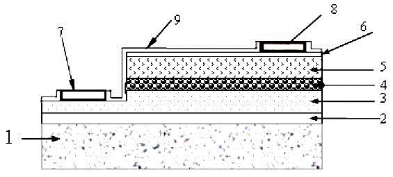
上述发射圆偏振光的LED芯片的结构如图1所示,包括衬底基片1,在衬底基片1上设有缓冲层2,在缓冲层2的上设有非磁性的半导体底层3,在半导体底层3上设有发光层4,在发光层4上设有磁性半导体顶层5,在磁性半导体顶层5上设有透明电极层6;在半导体底层3及透明电极层6上分别连接有底层电极7及顶层电极8;在外部设有露出底层电极7及顶层电极8顶面的钝化保护层9。
The structure of the above-mentioned LED chip emitting circularly polarized light is as shown in Figure 1, comprising a
上述发射圆偏振光的LED芯片的制备方法:a对衬底基片进行处理:先将蓝宝石作为材料的衬底基片在1100℃下烘烤20min,然后在800℃下对衬底基片进行100s的氮化处理;b生长n型一侧薄膜:在经过处理的衬底基片上采用MOCVD法,在800℃的条件下,生长厚度为8nm的AlN缓冲层;600℃的条件下,生长厚度为2um的GaN缓冲层;在600℃的条件下,生长厚度为100nm的GaN层;在600℃的条件下,掺杂Si生长厚度为100nm的n型GaN层;c生长多量子阱发光层:1)在600℃的条件下,生长厚度为50nm的GaN层;2)600℃的条件下,生长厚度为10nm的氮化镓铟(InGaN)发光层;3)在600℃的条件下,生长厚度为50nm的GaN层;4)将步骤2)及步骤3)重复10个周期,最后一个GaN层可以为P型;d采用MBE法生长p型(Ga1-xMnx)N磁性半导体薄膜:在240℃的条件下,利用共掺杂方式加入Mn以及比N原子半径小的Mg,生长厚度为80nm的p型Ga1-xMnxN顶接触层(x=3%~5%);在略低于生长温度的条件下退火1小时,得到的外延片结构见附图3;e清洗:使用H2SO4溶液、H2O2溶液、氢氟酸溶液、盐酸、NH4OH等结合超声波清洗技术去除所述LED外延片表面的有机杂质和金属离子;f沉积透明电极层:采用溅射法在p型(Ga1-xMnx)N磁性半导体薄膜上沉积一层ITO透明电极,厚度为200nm;g去除n区的透明电极层:在ITO上涂一层光刻胶,对n区的方形区域进行光刻、刻蚀,刻蚀方法为反应离子刻蚀(RIE),刻蚀完毕后除去光刻胶;h对n电极区平台光刻、刻蚀:对芯片进行清洗后,涂厚的光刻胶;在附图4所示n区位置光刻出一个需要的几何区域,其位置也根据需要可调;刻蚀出比较深的n侧电极区平台,既要保证刻蚀到n型GaN裸露,又不能将n型GaN层刻穿;刻蚀的方法采用增强等离子刻蚀(ICP)法;刻蚀完毕后去除光刻胶,退火处理;i沉积p区和n区电极:对芯片进行清洗后,采用磁控溅射的方法在p型(Ga1-xMnx)N层和n型GaN区沉积Cu电极,厚度为200nm;对芯片进行清洗后,涂光刻胶,针对p区和n区的金属电极进行光刻、刻蚀;剥离残留的光刻胶,进行退火处理,得到的结构见附图5;j制备SiO2保护层:对芯片进行清洗后,用MOCVD设备生长一层SiO2保护层。涂光刻胶,对n电极和p电极的露出部分的图形进行光刻;用氟化氢(HF)溶液对电极区的SiO2进行刻蚀,完毕后除去光刻胶;k芯片的后期处理:对芯片的蓝宝石衬底进行研磨、减薄、划片、切割和成品测试等工序,最后对芯片进行封装。 The preparation method of the LED chip emitting circularly polarized light above: a. Treat the substrate substrate: first bake the substrate substrate made of sapphire at 1100° C. for 20 minutes, and then treat the substrate substrate at 800° C. Nitriding treatment for 100s; b. Growth of n-type thin film on one side: use MOCVD method on the treated substrate to grow an AlN buffer layer with a thickness of 8nm at 800°C; grow a thickness of 8nm at 600°C 2um GaN buffer layer; at 600°C, grow a GaN layer with a thickness of 100nm; at 600°C, grow an n-type GaN layer with a thickness of 100nm by doping Si; c grow a multi-quantum well light-emitting layer: 1) At 600°C, grow a GaN layer with a thickness of 50nm; 2) At 600°C, grow an indium gallium nitride (InGaN) light-emitting layer with a thickness of 10nm; 3) At 600°C, grow GaN layer with a thickness of 50nm; 4) Step 2) and step 3) are repeated for 10 cycles, and the last GaN layer can be P-type; d Use MBE method to grow p-type (Ga 1-x Mn x ) N magnetic semiconductor film : Under the condition of 240°C, the p-type Ga 1-x Mn x N top contact layer with a thickness of 80nm was grown by adding Mn and Mg with a smaller atomic radius than N by co-doping (x=3%~5%) ;Annealed for 1 hour under the condition slightly lower than the growth temperature, and the obtained epitaxial wafer structure is shown in Figure 3; e cleaning: use H 2 SO 4 solution, H 2 O 2 solution, hydrofluoric acid solution, hydrochloric acid, NH 4 OH etc. combined with ultrasonic cleaning technology to remove organic impurities and metal ions on the surface of the LED epitaxial wafer; f Deposition of a transparent electrode layer: a layer of transparent ITO was deposited on the p-type (Ga 1-x Mn x ) N magnetic semiconductor film by sputtering Electrode with a thickness of 200nm; gRemove the transparent electrode layer in the n-region: apply a layer of photoresist on the ITO, and perform photolithography and etching on the square area of the n-region. The etching method is reactive ion etching (RIE), Remove the photoresist after the etching is completed; h photoetch and etch the platform of the n electrode area: after cleaning the chip, apply a thick photoresist; photoetch a required geometry at the position of the n area shown in Figure 4 area, its position can also be adjusted according to needs; etch out a relatively deep n-side electrode area platform, it is necessary to ensure that the n-type GaN is etched to be exposed, and the n-type GaN layer cannot be etched through; the etching method adopts enhanced plasma Etching (ICP) method; remove the photoresist after etching, annealing treatment; i deposit p-region and n-region electrodes: after cleaning the chip, use magnetron sputtering method on the p-type (Ga 1-x Mn x ) Deposit Cu electrodes on the N layer and n-type GaN region with a thickness of 200nm; after cleaning the chip, apply photoresist, and perform photolithography and etching on the metal electrodes in the p-region and n-region; peel off the remaining photoresist , for annealing treatment, the obtained structure is shown in accompanying drawing 5; j preparation of SiO 2 protective layer: after cleaning the chip, use M OCVD equipment grows a protective layer of SiO 2 . Apply photoresist, and perform photolithography on the exposed part of the n-electrode and p-electrode; use hydrogen fluoride (HF) solution to etch the SiO 2 in the electrode area, and remove the photoresist after completion; post-processing of the k-chip: The sapphire substrate of the chip undergoes processes such as grinding, thinning, scribing, cutting, and finished product testing, and finally the chip is packaged.
按照所述步骤和工艺,能够制备出含质量较好的p型Ga1-xMnxN磁性薄膜的LED芯片,其中的p型磁性半导体薄膜与发光层上方的GaN构成异质结,成为极化自旋空穴注入器。通过该磁性自旋载流子注入器,可以向发光层注入极化空穴,到达发光层的极化自旋空穴与n型GaN提供的未极化的电子发生辐射复合发射出圆偏振光。 According to the above steps and process, an LED chip containing a p-type Ga 1-x Mn x N magnetic film with good quality can be prepared, in which the p-type magnetic semiconductor film and GaN above the light-emitting layer form a heterojunction, forming a pole spin-hole injector. Through the magnetic spin carrier injector, polarized holes can be injected into the light-emitting layer, and the polarized spin holes reaching the light-emitting layer can radiatively recombine with the unpolarized electrons provided by n-type GaN to emit circularly polarized light. .
通过调整发光层结构及材料组分可以发出不同颜色的圆偏振光。 Circularly polarized light of different colors can be emitted by adjusting the structure and material components of the light-emitting layer. the
本发明的实施例2:发射圆偏振光的LED芯片,芯片的顶层为p型磁性层、底层为n型磁性层,即将顶部的p型层及底部的n型层中掺杂Fe,同时在p型层中加入Zn降低受主补偿、在n型层中加入Si增加施主电荷,使顶层的p型层及底部的n型层成为具有磁性的半导体层,p型层及n型层同时为发光层提供自旋载流子注入,输运到发光层中辐射复合,使发光层发出圆偏振光(发光层为5个周期的氮化镓铟(GaInN/GaN)多量子阱结构)。
上述可发射圆偏振光的LED芯片的制备方法为,a对衬底基片进行处理:先将蓝宝石作为材料的衬底基片在1000℃下烘烤22min,然后在500℃下对衬底基片进行160s的氮化处理;b生长n型一侧薄膜:在经过处理的衬底基片上采用MOCVD法,在500℃的条件下,生长厚度为10nm的AlN缓冲层;500℃的条件下,生长厚度为2um的GaN缓冲层;在500℃的条件下,生长厚度为200nm的GaN层;在500℃的条件下,掺杂Fe及Si生长厚度为200nm的n型(Ga1-xFex)N层(x=3%~5%);c生长多量子阱发光层:1)在500℃的条件下,生长厚度为100nm的GaN层;2)500℃的条件下,生长厚度为15nm的氮化镓铟(InGaN)发光层;3)在500℃的条件下,生长厚度为100nm的GaN层;4)将步骤2)及步骤3)重复5个周期,最后一个GaN层可以为P型;d采用MOCVD法生长p型(Ga1-xFex)N磁性半导体薄膜:在500℃的条件下,利用共掺杂方式加入Fe以及Zn,生长厚度为80nm的p型(Ga1-xFex)N顶接触层(x=2.5%~5%); e清洗:使用H2SO4溶液、H2O2溶液、氢氟酸溶液、盐酸、NH4OH等结合超声波清洗技术去除所述LED外延片表面的有机杂质和金属离子;f沉积透明电极层:采用溅射法在p型(Ga1-xFex)N磁性半导体薄膜上沉积一层ITO透明电极,厚度为200nm;去除n区的透明电极层。在ITO上涂一层光刻胶, 对n区的方形区域进行光刻、刻蚀,刻蚀方法为反应离子刻蚀(RIE),刻蚀完毕后除去光刻胶;g对n电极区平台光刻、刻蚀:对芯片进行清洗后,涂厚的光刻胶;在n区位置光刻出一个需要的几何区域,其位置也根据需要可调;刻蚀出比较深的n侧电极区平台,既要保证刻蚀到n型GaN裸露,又不能将n型GaN层刻穿;刻蚀的方法采用增强等离子刻蚀(ICP)法;刻蚀完毕后去除光刻胶,退火处理;h沉积p区和n区电极:对芯片进行清洗后,采用磁控溅射的方法在p型(Ga1-xFex)N层和n型(Ga1-xFex)N区沉积Au电极,厚度为200nm;对芯片进行清洗后,涂光刻胶,针对p区和n区的金属电极进行光刻、刻蚀;剥离残留的光刻胶,进行退火处理;i制备SiO2保护层:对芯片进行清洗后,用MOCVD设备生长一层SiO2保护层。涂光刻胶,对n电极和p电极的露出部分的图形进行光刻;用氟化氢(HF)溶液对电极区的SiO2进行刻蚀,完毕后除去光刻胶;j芯片的后期处理:对芯片的蓝宝石衬底进行研磨、减薄、划片、切割和成品测试等工序,最后对芯片进行封装。 The preparation method of the above-mentioned LED chip that can emit circularly polarized light is as follows: a. Treat the substrate substrate: first bake the substrate substrate made of sapphire at 1000° C. for 22 minutes, and then bake the substrate substrate at 500° C. Nitriding the wafer for 160s; b. Growth of n-type thin film on one side: grow an AlN buffer layer with a thickness of 10nm on the treated substrate by MOCVD at 500°C; Grow a GaN buffer layer with a thickness of 2um; grow a GaN layer with a thickness of 200nm at 500°C; grow an n-type (Ga 1-x Fe x ) N layer (x = 3% ~ 5%); c growth multi-quantum well light-emitting layer: 1) under the condition of 500°C, grow a GaN layer with a thickness of 100nm; 2) under the condition of 500°C, grow a thickness of 15nm Indium gallium nitride (InGaN) light-emitting layer; 3) Under the condition of 500°C, grow a GaN layer with a thickness of 100nm; 4) Repeat step 2) and step 3) for 5 cycles, and the last GaN layer can be P type; d grow p-type (Ga 1-x Fe x ) N magnetic semiconductor film by MOCVD method: under the condition of 500 ℃, add Fe and Zn by co-doping, and grow a p-type (Ga 1 -x Fe x ) N magnetic semiconductor film with a thickness of 80nm. x Fe x ) N top contact layer (x=2.5%~5%); e cleaning: use H 2 SO 4 solution, H 2 O 2 solution, hydrofluoric acid solution, hydrochloric acid, NH 4 OH, etc. combined with ultrasonic cleaning technology to remove Organic impurities and metal ions on the surface of the LED epitaxial wafer; f deposition of a transparent electrode layer: a layer of ITO transparent electrode is deposited on the p-type (Ga 1-x Fe x ) N magnetic semiconductor film by sputtering, with a thickness of 200nm; The transparent electrode layer of the n-region is removed. Coat a layer of photoresist on the ITO, and perform photolithography and etching on the square area of the n region. The etching method is reactive ion etching (RIE), and the photoresist is removed after etching; g is for the platform of the n electrode region Photolithography and etching: After cleaning the chip, apply a thick photoresist; photoetch a required geometric area at the n-zone position, and its position can also be adjusted according to needs; etch a relatively deep n-side electrode area The platform must be etched until the n-type GaN is exposed, and the n-type GaN layer cannot be etched through; the etching method adopts the enhanced plasma etching (ICP) method; after the etching is completed, the photoresist is removed and annealed; h Deposit p-region and n-region electrodes: After cleaning the chip, deposit Au electrodes on the p-type (Ga 1-x Fe x ) N layer and n-type (Ga 1-x Fex ) N region by magnetron sputtering , with a thickness of 200nm; after cleaning the chip, apply photoresist, and carry out photolithography and etching for the metal electrodes in p and n regions; peel off the remaining photoresist, and perform annealing treatment; i prepare SiO 2 protective layer: After cleaning the chip, grow a layer of SiO 2 protective layer with MOCVD equipment. Apply photoresist, and perform photolithography on the exposed part of the n-electrode and p-electrode; use hydrogen fluoride (HF) solution to etch the SiO 2 in the electrode area, and remove the photoresist after completion; post-processing of the j chip: The sapphire substrate of the chip undergoes processes such as grinding, thinning, scribing, cutting, and finished product testing, and finally the chip is packaged.
本发明的实施例3:发射圆偏振光的LED芯片,芯片为反转的LED外延层结构,即顶层为n型磁性层的LED芯片。方法是将顶部的n型层中掺杂Co和Si、底部p型层中加入Mg,使顶层的n型层成为具有磁性的半导体层,该n型层为发光层提供自旋载流子(电子)注入,输运到发光层中的自旋载流子与p型层中输运的未自旋极化的载流子(空穴)辐射复合,使发光层发出圆偏振光(发光层为15个周期的氮化镓铟(GaInN/GaN)多量子阱结构)。
上述可发射圆偏振光的LED芯片的制备方法为,a对衬底基片进行处理:先将蓝宝石作为材料的衬底基片在1200℃下烘烤18min,然后在1000℃下对衬底基片进行60s的氮化处理;b生长p型层一侧薄膜:在经过处理的衬底基片上采用MOCVD法,在1000℃的条件下,生长厚度为5nm的AlN缓冲层;700℃的条件下,生长厚度为2um的GaN缓冲层;在700℃的条件下,生长厚度为50nm的GaN层;在700℃的条件下,掺杂Mg生长厚度为50nm的p型GaN层;c生长多量子阱发光层:1)在650℃的条件下,生长厚度为100nm的GaN层;2)650℃的条件下,生长厚度为5nm的氮化镓铟(InGaN)发光层;3)在650℃的条件下,生长厚度为100nm的GaN层;4)将步骤2)及步骤3)重复15个周期;d采用MBE法生长n型(Ga1-xCox)N磁性半导体薄膜:在220℃的条件下,利用共掺杂方式加入Co以及Si,生长厚度为20nm的p型(Ga1-xCox)N顶接触层(x=3%~5%);在略低于生长温度的条件下退火1小时;e清洗:使用H2SO4溶液、H2O2溶液、氢氟酸溶液、盐酸、NH4OH等结合超声波清洗技术去除所述LED外延片表面的有机杂质和金属离子;f沉积透明电极层:采用溅射法在n型(Ga1-xCox)N磁性半导体薄膜上沉积一层ITO透明电极,厚度为200nm;g去除p区的透明电极层:在ITO上涂一层光刻胶,对p区的方形区域进行光刻、刻蚀,刻蚀方法为反应离子刻蚀(RIE),刻蚀完毕后除去光刻胶;h对p电极区平台光刻、刻蚀:对芯片进行清洗后,涂厚的光刻胶;在p区位置光刻出一个需要的几何区域,其位置也根据需要可调;刻蚀出比较深的p侧电极区平台,既要保证刻蚀到p型GaN裸露,又不能将p型GaN层刻穿;刻蚀的方法采用增强等离子刻蚀(ICP)法;刻蚀完毕后去除光刻胶,退火处理;i沉积p区和n区电极:对芯片进行清洗后,采用磁控溅射的方法在n型((Ga1-xCox)N层和p型GaN区沉积Cu电极,厚度为200nm;对芯片进行清洗后,涂光刻胶,针对p区和n区的金属电极进行光刻、刻蚀;剥离残留的光刻胶,进行退火处理;j制备SiO2保护层:对芯片进行清洗后,用MOCVD设备生长一层SiO2保护层。涂光刻胶,对n电极和p电极的露出部分的图形进行光刻;用氟化氢(HF)溶液对电极区的SiO2进行刻蚀,完毕后除去光刻胶;k芯片的后期处理:对芯片的蓝宝石衬底进行研磨、减薄、划片、切割和成品测试等工序,最后对芯片进行封装。 The preparation method of the above-mentioned LED chip that can emit circularly polarized light is as follows: a. Treat the substrate substrate: first bake the substrate substrate made of sapphire at 1200° C. for 18 minutes, and then bake the substrate substrate at 1000° C. Nitriding treatment of the wafer for 60s; b Growth of thin film on the side of the p-type layer: grow an AlN buffer layer with a thickness of 5nm under the condition of 1000°C by MOCVD method on the treated substrate; under the condition of 700°C , grow a GaN buffer layer with a thickness of 2um; grow a GaN layer with a thickness of 50nm under the condition of 700°C; grow a p-type GaN layer with a thickness of 50nm under the condition of 700°C; grow multiple quantum wells Light-emitting layer: 1) at 650°C, grow a GaN layer with a thickness of 100nm; 2) at 650°C, grow an indium gallium nitride (InGaN) light-emitting layer with a thickness of 5nm; 3) at 650°C 4) Repeat step 2) and step 3) for 15 cycles; d Use MBE method to grow n-type (Ga 1-x Co x ) N magnetic semiconductor film: at 220°C Next, Co and Si are added by co-doping to grow a p-type (Ga 1-x Co x ) N top contact layer (x=3%-5%) with a thickness of 20nm; under conditions slightly lower than the growth temperature Annealing for 1 hour; e cleaning: using H 2 SO 4 solution, H 2 O 2 solution, hydrofluoric acid solution, hydrochloric acid, NH 4 OH, etc. in combination with ultrasonic cleaning technology to remove organic impurities and metal ions on the surface of the LED epitaxial wafer; f Deposit transparent electrode layer: Deposit a layer of ITO transparent electrode on the n-type (Ga 1-x Co x ) N magnetic semiconductor film by sputtering method, with a thickness of 200nm; g remove the transparent electrode layer in the p region: apply a layer of photoresist, photolithography and etching are performed on the square area of the p region, the etching method is reactive ion etching (RIE), and the photoresist is removed after etching; h photolithography and etching of the p electrode region platform : After cleaning the chip, apply thick photoresist; photoetch a required geometric area in the p area, and its position can also be adjusted according to needs; etch out a relatively deep p-side electrode area platform, which must ensure Etch until the p-type GaN is exposed, but the p-type GaN layer cannot be etched through; the etching method adopts the enhanced plasma etching (ICP) method; after the etching is completed, the photoresist is removed and annealed; Area electrode: After cleaning the chip, use magnetron sputtering to deposit Cu electrodes on the n-type ((Ga 1-x Co x ) N layer and p-type GaN area with a thickness of 200nm; after cleaning the chip, coat Photoresist, perform photolithography and etching for the metal electrodes in the p-region and n-region; peel off the remaining photoresist and perform annealing treatment; j prepare SiO 2 protective layer: after cleaning the chip, grow a layer with MOCVD equipment SiO 2 protective layer. Apply photoresist, and perform photolithography on the exposed part of the n-electrode and p-electrode ; Use hydrogen fluoride (HF) solution to etch the SiO 2 in the electrode area, and remove the photoresist after completion; post-processing of k chip: grinding, thinning, scribing, cutting and finished product testing on the sapphire substrate of the chip, etc. process, and finally package the chip.
按照所述步骤和工艺,能够制备出含质量较好的n型(Ga1-xCox)N磁性薄膜的LED芯片,其中的n型(Ga1-xCox)N磁性半导体薄膜与发光层上方的GaN构成异质结,成为极化自旋电子注入器,通过该磁性自旋载流子注入器,可以向发光层注入极化电子,到达发光层的极化自旋电子与p型GaN提供的未极化的空穴发生辐射复合发射出圆偏振光。 According to the steps and process, it is possible to prepare an LED chip containing n-type (Ga 1-x Co x ) N magnetic film with good quality, in which the n-type (Ga 1-x Co x ) N magnetic semiconductor film is compatible with luminescence The GaN above the layer forms a heterojunction and becomes a polarized spin electron injector. Through this magnetic spin carrier injector, polarized electrons can be injected into the light-emitting layer, and the polarized spin electrons reaching the light-emitting layer and the p-type The unpolarized holes provided by GaN undergo radiative recombination to emit circularly polarized light.
Claims (10)
Priority Applications (1)
| Application Number | Priority Date | Filing Date | Title |
|---|---|---|---|
| CN201110190102.0A CN102255015B (en) | 2011-07-08 | 2011-07-08 | Method for emitting circularly polarized light using LED (light-emitting diode) chip, and product and preparation method thereof |
Applications Claiming Priority (1)
| Application Number | Priority Date | Filing Date | Title |
|---|---|---|---|
| CN201110190102.0A CN102255015B (en) | 2011-07-08 | 2011-07-08 | Method for emitting circularly polarized light using LED (light-emitting diode) chip, and product and preparation method thereof |
Publications (2)
| Publication Number | Publication Date |
|---|---|
| CN102255015A true CN102255015A (en) | 2011-11-23 |
| CN102255015B CN102255015B (en) | 2014-04-09 |
Family
ID=44982127
Family Applications (1)
| Application Number | Title | Priority Date | Filing Date |
|---|---|---|---|
| CN201110190102.0A Expired - Fee Related CN102255015B (en) | 2011-07-08 | 2011-07-08 | Method for emitting circularly polarized light using LED (light-emitting diode) chip, and product and preparation method thereof |
Country Status (1)
| Country | Link |
|---|---|
| CN (1) | CN102255015B (en) |
Cited By (7)
| Publication number | Priority date | Publication date | Assignee | Title |
|---|---|---|---|---|
| CN105047771A (en) * | 2015-07-10 | 2015-11-11 | 厦门市三安光电科技有限公司 | Nitride light emitting diode |
| CN107658269A (en) * | 2017-08-24 | 2018-02-02 | 华灿光电(浙江)有限公司 | A light-emitting diode chip and its manufacturing method |
| CN108110099A (en) * | 2017-04-01 | 2018-06-01 | 厦门乾照光电股份有限公司 | A kind of LED chip and preparation method thereof |
| CN109742249A (en) * | 2018-12-26 | 2019-05-10 | 深圳市华星光电半导体显示技术有限公司 | Quantum dot LED and manufacturing method thereof |
| CN110071197A (en) * | 2019-03-27 | 2019-07-30 | 北京大学 | A kind of high polarization degree spin LED and preparation method thereof based on non-polar plane gallium nitride |
| CN112753108A (en) * | 2018-09-28 | 2021-05-04 | 同和电子科技有限公司 | Group III nitride semiconductor light-emitting element and method for manufacturing same |
| CN120728371A (en) * | 2025-08-28 | 2025-09-30 | 武汉鑫威源电子科技有限公司 | A gallium nitride-based laser with high electrical injection efficiency and its preparation method and device |
Citations (6)
| Publication number | Priority date | Publication date | Assignee | Title |
|---|---|---|---|---|
| US20060186432A1 (en) * | 2005-02-18 | 2006-08-24 | Osipov Viatcheslav V | Polarized radiation source using spin extraction/injection |
| CN101319400A (en) * | 2008-05-19 | 2008-12-10 | 南京大学 | A kind of method and application of Fe-doped growth GaFeN dilute magnetic semiconductor |
| CN101350385A (en) * | 2007-07-17 | 2009-01-21 | 北京大学 | A GaN-based spin light-emitting diode and its preparation method |
| CN101572286A (en) * | 2009-05-27 | 2009-11-04 | 苏州大学 | Polarized light-emitting diode |
| TW201103161A (en) * | 2009-07-01 | 2011-01-16 | Long-Jian Chen | Spin-injection gallium-nitride LED and its manufacturing method |
| CN202120976U (en) * | 2011-07-08 | 2012-01-18 | 贵州大学 | LED chip for emitting circularly polarized light |
-
2011
- 2011-07-08 CN CN201110190102.0A patent/CN102255015B/en not_active Expired - Fee Related
Patent Citations (6)
| Publication number | Priority date | Publication date | Assignee | Title |
|---|---|---|---|---|
| US20060186432A1 (en) * | 2005-02-18 | 2006-08-24 | Osipov Viatcheslav V | Polarized radiation source using spin extraction/injection |
| CN101350385A (en) * | 2007-07-17 | 2009-01-21 | 北京大学 | A GaN-based spin light-emitting diode and its preparation method |
| CN101319400A (en) * | 2008-05-19 | 2008-12-10 | 南京大学 | A kind of method and application of Fe-doped growth GaFeN dilute magnetic semiconductor |
| CN101572286A (en) * | 2009-05-27 | 2009-11-04 | 苏州大学 | Polarized light-emitting diode |
| TW201103161A (en) * | 2009-07-01 | 2011-01-16 | Long-Jian Chen | Spin-injection gallium-nitride LED and its manufacturing method |
| CN202120976U (en) * | 2011-07-08 | 2012-01-18 | 贵州大学 | LED chip for emitting circularly polarized light |
Non-Patent Citations (2)
| Title |
|---|
| SJPEARTON等: "Wide bandgap GaN-based semiconductors for spintronics", 《JOURNAL OF PHYSICS: CONDENSED MATTER》 * |
| 崔旭高 等: "自旋发光二极管原型器件的设计和制备", 《第十一届全国MOCVD学术会议》 * |
Cited By (11)
| Publication number | Priority date | Publication date | Assignee | Title |
|---|---|---|---|---|
| CN105047771A (en) * | 2015-07-10 | 2015-11-11 | 厦门市三安光电科技有限公司 | Nitride light emitting diode |
| CN105047771B (en) * | 2015-07-10 | 2018-04-06 | 厦门市三安光电科技有限公司 | A kind of iii-nitride light emitting devices |
| CN108110099A (en) * | 2017-04-01 | 2018-06-01 | 厦门乾照光电股份有限公司 | A kind of LED chip and preparation method thereof |
| CN108110099B (en) * | 2017-04-01 | 2019-03-12 | 厦门乾照光电股份有限公司 | A kind of LED chip and preparation method thereof |
| CN107658269A (en) * | 2017-08-24 | 2018-02-02 | 华灿光电(浙江)有限公司 | A light-emitting diode chip and its manufacturing method |
| CN107658269B (en) * | 2017-08-24 | 2020-09-08 | 华灿光电(浙江)有限公司 | A kind of chip of light-emitting diode and preparation method thereof |
| CN112753108A (en) * | 2018-09-28 | 2021-05-04 | 同和电子科技有限公司 | Group III nitride semiconductor light-emitting element and method for manufacturing same |
| CN109742249A (en) * | 2018-12-26 | 2019-05-10 | 深圳市华星光电半导体显示技术有限公司 | Quantum dot LED and manufacturing method thereof |
| CN110071197A (en) * | 2019-03-27 | 2019-07-30 | 北京大学 | A kind of high polarization degree spin LED and preparation method thereof based on non-polar plane gallium nitride |
| CN120728371A (en) * | 2025-08-28 | 2025-09-30 | 武汉鑫威源电子科技有限公司 | A gallium nitride-based laser with high electrical injection efficiency and its preparation method and device |
| CN120728371B (en) * | 2025-08-28 | 2025-12-23 | 武汉鑫威源电子科技有限公司 | Gallium nitride-based laser with high electric injection efficiency and preparation method and device thereof |
Also Published As
| Publication number | Publication date |
|---|---|
| CN102255015B (en) | 2014-04-09 |
Similar Documents
| Publication | Publication Date | Title |
|---|---|---|
| Pandey et al. | An ultrahigh efficiency excitonic micro-LED | |
| TWI385822B (en) | Method for manufacturing group III nitride semiconductor layer, and group III nitride semiconductor light-emitting device, and lamp | |
| KR101067122B1 (en) | Method of manufacturing group III nitride semiconductor, method of manufacturing group III nitride semiconductor light emitting device and group III nitride semiconductor light emitting device, and lamp | |
| CN102368519B (en) | A kind of method improving semiconductor diode multiple quantum well light emitting efficiency | |
| CN102185056B (en) | Gallium-nitride-based light emitting diode capable of improving electron injection efficiency | |
| JPH04199752A (en) | Compound semiconductor light emitting device and its manufacturing method | |
| CN111403566B (en) | Light-emitting diode device structure with sidewall field plate and preparation method thereof | |
| CN102255015A (en) | Method for emitting circularly polarized light using LED (light-emitting diode) chip, and product and preparation method thereof | |
| CN106784216A (en) | Epitaxial wafer of GaN-based light emitting diode and growth method thereof | |
| CN106653971B (en) | Epitaxial wafer of GaN-based light emitting diode and growth method thereof | |
| CN105206726A (en) | LED structure and growth method thereof | |
| CN102280547A (en) | GaN semiconductor luminotron with P-type active region | |
| CN106711295A (en) | Growth method of GaN-based light emitting diode epitaxial wafer | |
| CN109346583A (en) | A kind of light-emitting diode epitaxial wafer and preparation method thereof | |
| CN109411579B (en) | Semiconductor device with graphene structure and preparation method thereof | |
| JP2009283620A (en) | Group iii nitride semiconductor light emitting element, method for manufacturing thereof, and lamp | |
| CN105702829A (en) | Light emitting diode epitaxy structure provided with P-type ohmic contact layer | |
| CN106601883A (en) | Epitaxial wafer of light emitting diode and preparation method | |
| CN106876530B (en) | Epitaxial wafer of gallium nitride-based light-emitting diode and manufacturing method thereof | |
| Xing et al. | Achieving InGaN-based red light-emitting diodes by increasing the growth pressure of quantum wells | |
| CN112701196B (en) | AlGaN-based semiconductor ultraviolet device and its preparation method | |
| KR101030823B1 (en) | Transparent thin film, light emitting device comprising same and manufacturing method thereof | |
| CN107799631B (en) | High-brightness LED preparation process | |
| CN106409996A (en) | Epitaxial growth method capable of improving LED chip property uniformity | |
| CN108987544A (en) | A kind of LED epitaxial slice and its manufacturing method |
Legal Events
| Date | Code | Title | Description |
|---|---|---|---|
| C06 | Publication | ||
| PB01 | Publication | ||
| C10 | Entry into substantive examination | ||
| SE01 | Entry into force of request for substantive examination | ||
| C14 | Grant of patent or utility model | ||
| GR01 | Patent grant | ||
| CF01 | Termination of patent right due to non-payment of annual fee | ||
| CF01 | Termination of patent right due to non-payment of annual fee |
Granted publication date: 20140409 Termination date: 20200708 |