CN102243921A - Dye-sensitized solar cell with metal wire layer and electrode thereof - Google Patents
Dye-sensitized solar cell with metal wire layer and electrode thereof Download PDFInfo
- Publication number
- CN102243921A CN102243921A CN 201010180990 CN201010180990A CN102243921A CN 102243921 A CN102243921 A CN 102243921A CN 201010180990 CN201010180990 CN 201010180990 CN 201010180990 A CN201010180990 A CN 201010180990A CN 102243921 A CN102243921 A CN 102243921A
- Authority
- CN
- China
- Prior art keywords
- electrode
- layer
- metal
- combination
- catalyst
- Prior art date
- Legal status (The legal status is an assumption and is not a legal conclusion. Google has not performed a legal analysis and makes no representation as to the accuracy of the status listed.)
- Pending
Links
- 229910052751 metal Inorganic materials 0.000 title claims abstract description 85
- 239000002184 metal Substances 0.000 title claims abstract description 85
- 239000000758 substrate Substances 0.000 claims abstract description 65
- 239000000463 material Substances 0.000 claims abstract description 42
- 239000003054 catalyst Substances 0.000 claims abstract description 33
- PXHVJJICTQNCMI-UHFFFAOYSA-N Nickel Chemical compound [Ni] PXHVJJICTQNCMI-UHFFFAOYSA-N 0.000 claims abstract description 31
- 239000003792 electrolyte Substances 0.000 claims abstract description 20
- 239000010936 titanium Substances 0.000 claims abstract description 20
- RTAQQCXQSZGOHL-UHFFFAOYSA-N Titanium Chemical compound [Ti] RTAQQCXQSZGOHL-UHFFFAOYSA-N 0.000 claims abstract description 16
- 229910052719 titanium Inorganic materials 0.000 claims abstract description 16
- XAGFODPZIPBFFR-UHFFFAOYSA-N aluminium Chemical compound [Al] XAGFODPZIPBFFR-UHFFFAOYSA-N 0.000 claims abstract description 15
- 229910052782 aluminium Inorganic materials 0.000 claims abstract description 14
- 229910052759 nickel Inorganic materials 0.000 claims abstract description 12
- XLOMVQKBTHCTTD-UHFFFAOYSA-N Zinc monoxide Chemical compound [Zn]=O XLOMVQKBTHCTTD-UHFFFAOYSA-N 0.000 claims description 31
- GWEVSGVZZGPLCZ-UHFFFAOYSA-N Titan oxide Chemical compound O=[Ti]=O GWEVSGVZZGPLCZ-UHFFFAOYSA-N 0.000 claims description 21
- 239000000975 dye Substances 0.000 claims description 16
- 239000011787 zinc oxide Substances 0.000 claims description 15
- BASFCYQUMIYNBI-UHFFFAOYSA-N platinum Chemical group [Pt] BASFCYQUMIYNBI-UHFFFAOYSA-N 0.000 claims description 10
- 239000011521 glass Substances 0.000 claims description 9
- 239000004033 plastic Substances 0.000 claims description 9
- 229920003023 plastic Polymers 0.000 claims description 9
- XOLBLPGZBRYERU-UHFFFAOYSA-N tin dioxide Chemical compound O=[Sn]=O XOLBLPGZBRYERU-UHFFFAOYSA-N 0.000 claims description 9
- 229910001887 tin oxide Inorganic materials 0.000 claims description 9
- 239000004408 titanium dioxide Substances 0.000 claims description 9
- 239000004020 conductor Substances 0.000 claims description 7
- AMGQUBHHOARCQH-UHFFFAOYSA-N indium;oxotin Chemical compound [In].[Sn]=O AMGQUBHHOARCQH-UHFFFAOYSA-N 0.000 claims description 7
- 229910052755 nonmetal Inorganic materials 0.000 claims description 7
- 229910052697 platinum Inorganic materials 0.000 claims description 5
- MCMNRKCIXSYSNV-UHFFFAOYSA-N ZrO2 Inorganic materials O=[Zr]=O MCMNRKCIXSYSNV-UHFFFAOYSA-N 0.000 claims description 4
- INPLXZPZQSLHBR-UHFFFAOYSA-N cobalt(2+);sulfide Chemical group [S-2].[Co+2] INPLXZPZQSLHBR-UHFFFAOYSA-N 0.000 claims description 4
- RVTZCBVAJQQJTK-UHFFFAOYSA-N oxygen(2-);zirconium(4+) Chemical compound [O-2].[O-2].[Zr+4] RVTZCBVAJQQJTK-UHFFFAOYSA-N 0.000 claims description 4
- WWNBZGLDODTKEM-UHFFFAOYSA-N sulfanylidenenickel Chemical compound [Ni]=S WWNBZGLDODTKEM-UHFFFAOYSA-N 0.000 claims description 4
- YVTHLONGBIQYBO-UHFFFAOYSA-N zinc indium(3+) oxygen(2-) Chemical compound [O--].[Zn++].[In+3] YVTHLONGBIQYBO-UHFFFAOYSA-N 0.000 claims description 3
- 230000005693 optoelectronics Effects 0.000 claims 4
- 239000002904 solvent Substances 0.000 claims 4
- UCKMPCXJQFINFW-UHFFFAOYSA-N Sulphide Chemical compound [S-2] UCKMPCXJQFINFW-UHFFFAOYSA-N 0.000 claims 2
- 239000004411 aluminium Substances 0.000 claims 2
- 230000005284 excitation Effects 0.000 claims 2
- 230000003287 optical effect Effects 0.000 claims 2
- 238000001179 sorption measurement Methods 0.000 claims 2
- YCKRFDGAMUMZLT-UHFFFAOYSA-N Fluorine atom Chemical compound [F] YCKRFDGAMUMZLT-UHFFFAOYSA-N 0.000 claims 1
- 229910052787 antimony Inorganic materials 0.000 claims 1
- WATWJIUSRGPENY-UHFFFAOYSA-N antimony atom Chemical compound [Sb] WATWJIUSRGPENY-UHFFFAOYSA-N 0.000 claims 1
- 229910052731 fluorine Inorganic materials 0.000 claims 1
- 239000011737 fluorine Substances 0.000 claims 1
- 239000011248 coating agent Substances 0.000 abstract description 5
- 238000000576 coating method Methods 0.000 abstract description 5
- 239000010410 layer Substances 0.000 abstract 6
- 239000011241 protective layer Substances 0.000 abstract 1
- WEVYAHXRMPXWCK-UHFFFAOYSA-N Acetonitrile Chemical compound CC#N WEVYAHXRMPXWCK-UHFFFAOYSA-N 0.000 description 33
- 239000000243 solution Substances 0.000 description 16
- BQCADISMDOOEFD-UHFFFAOYSA-N Silver Chemical compound [Ag] BQCADISMDOOEFD-UHFFFAOYSA-N 0.000 description 12
- DKGAVHZHDRPRBM-UHFFFAOYSA-N Tert-Butanol Chemical compound CC(C)(C)O DKGAVHZHDRPRBM-UHFFFAOYSA-N 0.000 description 12
- -1 iodine ions Chemical class 0.000 description 10
- 230000001681 protective effect Effects 0.000 description 9
- 239000002105 nanoparticle Substances 0.000 description 8
- 229910010413 TiO 2 Inorganic materials 0.000 description 7
- 230000009975 flexible effect Effects 0.000 description 6
- 229910052709 silver Inorganic materials 0.000 description 6
- 239000004332 silver Substances 0.000 description 6
- 238000010586 diagram Methods 0.000 description 5
- 239000011630 iodine Substances 0.000 description 5
- 229910052740 iodine Inorganic materials 0.000 description 5
- 229920001169 thermoplastic Polymers 0.000 description 5
- 239000004416 thermosoftening plastic Substances 0.000 description 5
- 238000002834 transmittance Methods 0.000 description 5
- YEJRWHAVMIAJKC-UHFFFAOYSA-N 4-Butyrolactone Chemical compound O=C1CCCO1 YEJRWHAVMIAJKC-UHFFFAOYSA-N 0.000 description 4
- ZCYVEMRRCGMTRW-UHFFFAOYSA-N 7553-56-2 Chemical compound [I] ZCYVEMRRCGMTRW-UHFFFAOYSA-N 0.000 description 4
- IAZDPXIOMUYVGZ-UHFFFAOYSA-N Dimethylsulphoxide Chemical compound CS(C)=O IAZDPXIOMUYVGZ-UHFFFAOYSA-N 0.000 description 4
- 238000005229 chemical vapour deposition Methods 0.000 description 4
- 238000005516 engineering process Methods 0.000 description 4
- 238000001704 evaporation Methods 0.000 description 4
- 230000008020 evaporation Effects 0.000 description 4
- 238000000034 method Methods 0.000 description 4
- 239000011112 polyethylene naphthalate Substances 0.000 description 4
- 238000002360 preparation method Methods 0.000 description 4
- 238000006243 chemical reaction Methods 0.000 description 3
- 238000002513 implantation Methods 0.000 description 3
- 229920003207 poly(ethylene-2,6-naphthalate) Polymers 0.000 description 3
- 238000004544 sputter deposition Methods 0.000 description 3
- JJWJFWRFHDYQCN-UHFFFAOYSA-J 2-(4-carboxypyridin-2-yl)pyridine-4-carboxylate;ruthenium(2+);tetrabutylazanium;dithiocyanate Chemical compound [Ru+2].[S-]C#N.[S-]C#N.CCCC[N+](CCCC)(CCCC)CCCC.CCCC[N+](CCCC)(CCCC)CCCC.OC(=O)C1=CC=NC(C=2N=CC=C(C=2)C([O-])=O)=C1.OC(=O)C1=CC=NC(C=2N=CC=C(C=2)C([O-])=O)=C1 JJWJFWRFHDYQCN-UHFFFAOYSA-J 0.000 description 2
- LTNAYKNIZNSHQA-UHFFFAOYSA-L 2-(4-carboxypyridin-2-yl)pyridine-4-carboxylic acid;ruthenium(2+);dithiocyanate Chemical compound N#CS[Ru]SC#N.OC(=O)C1=CC=NC(C=2N=CC=C(C=2)C(O)=O)=C1.OC(=O)C1=CC=NC(C=2N=CC=C(C=2)C(O)=O)=C1 LTNAYKNIZNSHQA-UHFFFAOYSA-L 0.000 description 2
- YSHMQTRICHYLGF-UHFFFAOYSA-N 4-tert-butylpyridine Chemical compound CC(C)(C)C1=CC=NC=C1 YSHMQTRICHYLGF-UHFFFAOYSA-N 0.000 description 2
- AOFYLCZPMMOVJT-UHFFFAOYSA-N [Fe]([S])([S])[S] Chemical compound [Fe]([S])([S])[S] AOFYLCZPMMOVJT-UHFFFAOYSA-N 0.000 description 2
- 230000009286 beneficial effect Effects 0.000 description 2
- 239000003292 glue Substances 0.000 description 2
- ZJYYHGLJYGJLLN-UHFFFAOYSA-N guanidinium thiocyanate Chemical compound SC#N.NC(N)=N ZJYYHGLJYGJLLN-UHFFFAOYSA-N 0.000 description 2
- 239000007943 implant Substances 0.000 description 2
- 239000011259 mixed solution Substances 0.000 description 2
- 230000004048 modification Effects 0.000 description 2
- 238000012986 modification Methods 0.000 description 2
- 239000003960 organic solvent Substances 0.000 description 2
- 239000005022 packaging material Substances 0.000 description 2
- 229920000139 polyethylene terephthalate Polymers 0.000 description 2
- 239000005020 polyethylene terephthalate Substances 0.000 description 2
- 230000009467 reduction Effects 0.000 description 2
- 238000007789 sealing Methods 0.000 description 2
- 239000004065 semiconductor Substances 0.000 description 2
- 238000001771 vacuum deposition Methods 0.000 description 2
- 238000007740 vapor deposition Methods 0.000 description 2
- JKFYKCYQEWQPTM-UHFFFAOYSA-N 2-azaniumyl-2-(4-fluorophenyl)acetate Chemical compound OC(=O)C(N)C1=CC=C(F)C=C1 JKFYKCYQEWQPTM-UHFFFAOYSA-N 0.000 description 1
- UDKVCUREWCBQML-UHFFFAOYSA-N 3-methoxypropanenitrile Chemical compound COCCC#N.COCCC#N UDKVCUREWCBQML-UHFFFAOYSA-N 0.000 description 1
- ZKGNPQKYVKXMGJ-UHFFFAOYSA-N N,N-dimethylacetamide Chemical compound CN(C)C(C)=O.CN(C)C(C)=O ZKGNPQKYVKXMGJ-UHFFFAOYSA-N 0.000 description 1
- 206010070834 Sensitisation Diseases 0.000 description 1
- XUIMIQQOPSSXEZ-UHFFFAOYSA-N Silicon Chemical compound [Si] XUIMIQQOPSSXEZ-UHFFFAOYSA-N 0.000 description 1
- 229910021612 Silver iodide Inorganic materials 0.000 description 1
- 230000009471 action Effects 0.000 description 1
- 238000007796 conventional method Methods 0.000 description 1
- UXGNZZKBCMGWAZ-UHFFFAOYSA-N dimethylformamide dmf Chemical compound CN(C)C=O.CN(C)C=O UXGNZZKBCMGWAZ-UHFFFAOYSA-N 0.000 description 1
- 230000009977 dual effect Effects 0.000 description 1
- 238000007772 electroless plating Methods 0.000 description 1
- 239000008151 electrolyte solution Substances 0.000 description 1
- 238000005538 encapsulation Methods 0.000 description 1
- 230000007613 environmental effect Effects 0.000 description 1
- 150000002148 esters Chemical class 0.000 description 1
- 230000005283 ground state Effects 0.000 description 1
- XMBWDFGMSWQBCA-UHFFFAOYSA-N hydrogen iodide Chemical compound I XMBWDFGMSWQBCA-UHFFFAOYSA-N 0.000 description 1
- 230000006872 improvement Effects 0.000 description 1
- XMBWDFGMSWQBCA-UHFFFAOYSA-M iodide Chemical compound [I-] XMBWDFGMSWQBCA-UHFFFAOYSA-M 0.000 description 1
- 229940006461 iodide ion Drugs 0.000 description 1
- HSZCZNFXUDYRKD-UHFFFAOYSA-M lithium iodide Chemical compound [Li+].[I-] HSZCZNFXUDYRKD-UHFFFAOYSA-M 0.000 description 1
- 238000004519 manufacturing process Methods 0.000 description 1
- 239000003863 metallic catalyst Substances 0.000 description 1
- 150000002739 metals Chemical class 0.000 description 1
- 239000012811 non-conductive material Substances 0.000 description 1
- 230000005622 photoelectricity Effects 0.000 description 1
- 238000010248 power generation Methods 0.000 description 1
- 230000008569 process Effects 0.000 description 1
- 230000008313 sensitization Effects 0.000 description 1
- 229910052710 silicon Inorganic materials 0.000 description 1
- 239000010703 silicon Substances 0.000 description 1
- 229940045105 silver iodide Drugs 0.000 description 1
- 238000005245 sintering Methods 0.000 description 1
- 239000000126 substance Substances 0.000 description 1
- 238000005406 washing Methods 0.000 description 1
Images


Classifications
-
- Y—GENERAL TAGGING OF NEW TECHNOLOGICAL DEVELOPMENTS; GENERAL TAGGING OF CROSS-SECTIONAL TECHNOLOGIES SPANNING OVER SEVERAL SECTIONS OF THE IPC; TECHNICAL SUBJECTS COVERED BY FORMER USPC CROSS-REFERENCE ART COLLECTIONS [XRACs] AND DIGESTS
- Y02—TECHNOLOGIES OR APPLICATIONS FOR MITIGATION OR ADAPTATION AGAINST CLIMATE CHANGE
- Y02E—REDUCTION OF GREENHOUSE GAS [GHG] EMISSIONS, RELATED TO ENERGY GENERATION, TRANSMISSION OR DISTRIBUTION
- Y02E10/00—Energy generation through renewable energy sources
- Y02E10/50—Photovoltaic [PV] energy
- Y02E10/542—Dye sensitized solar cells
-
- Y—GENERAL TAGGING OF NEW TECHNOLOGICAL DEVELOPMENTS; GENERAL TAGGING OF CROSS-SECTIONAL TECHNOLOGIES SPANNING OVER SEVERAL SECTIONS OF THE IPC; TECHNICAL SUBJECTS COVERED BY FORMER USPC CROSS-REFERENCE ART COLLECTIONS [XRACs] AND DIGESTS
- Y02—TECHNOLOGIES OR APPLICATIONS FOR MITIGATION OR ADAPTATION AGAINST CLIMATE CHANGE
- Y02E—REDUCTION OF GREENHOUSE GAS [GHG] EMISSIONS, RELATED TO ENERGY GENERATION, TRANSMISSION OR DISTRIBUTION
- Y02E10/00—Energy generation through renewable energy sources
- Y02E10/50—Photovoltaic [PV] energy
- Y02E10/549—Organic PV cells
Landscapes
- Hybrid Cells (AREA)
Abstract
Description
技术领域 technical field
本发明关于用于电化学装置的电极的金属线层,尤指用于染料敏化太阳能电池的电极的金属线层。The present invention relates to a metal wire layer for an electrode of an electrochemical device, especially a metal wire layer for an electrode of a dye-sensitized solar cell.
背景技术 Background technique
在能源耗竭与环境保护的双重难题下,太阳能是极具潜力的绿色能源。由于硅晶太阳能电池的成本昂贵,使得具有低成本发电组件的染料敏化太阳能电池(dye-sensitized solar cell,DSSC)的技术开发逐渐受到重视。Under the dual problems of energy depletion and environmental protection, solar energy is a green energy with great potential. Due to the high cost of silicon solar cells, the technical development of dye-sensitized solar cells (DSSC) with low-cost power generation components has gradually attracted attention.
请参阅图1,染料敏化太阳能电池100的主要内部结构包含工作电极(阳极)110、对电极(阴极)120、电解质130。该阳极110包含导电基板111和接收太阳光能量的感光层112,而阴极120则包含导电基板121以及适当厚度的触媒层122。前述导电基板111、121视其基材113、123材质而定,例如:若前述基材113、123为非导电或导电性较差的材料,可分别于基材113、123上设有由导电材料所构成的导电层114和124;反之,若基材113、123为金属材质,则无须设置该导电层114及124。感光层112含有表面吸附有光激发染料的光电极材料,而电解质130的主要成分为含碘及碘离子的有机溶液。Referring to FIG. 1 , the main internal structure of a dye-sensitized solar cell 100 includes a working electrode (anode) 110 , a counter electrode (cathode) 120 , and an electrolyte 130 . The anode 110 includes a conductive substrate 111 and a photosensitive layer 112 for receiving sunlight energy, while the cathode 120 includes a conductive substrate 121 and a catalyst layer 122 with a proper thickness. The aforementioned conductive substrates 111, 121 depend on the materials of their base materials 113, 123. For example, if the aforementioned base materials 113, 123 are non-conductive or poorly conductive materials, conductive substrates 113, 123 can be provided with conductive substrates respectively. The conductive layers 114 and 124 are made of materials; on the contrary, if the substrates 113 and 123 are made of metal, the conductive layers 114 and 124 do not need to be provided. The photosensitive layer 112 contains photoelectrode materials with photoexcitable dyes adsorbed on the surface, and the main component of the electrolyte 130 is an organic solution containing iodine and iodine ions.
由于染料敏化太阳能电池的结构简单,因此若使用塑料或适当厚度的钛板作为基材113、123,所制成的染料敏化太阳能电池便可具可挠特性,适合于多种用途。除此之外,基材113、123亦可为玻璃材质。Due to the simple structure of the dye-sensitized solar cell, if plastic or a suitable thickness of titanium plate is used as the substrate 113 , 123 , the dye-sensitized solar cell can be flexible and suitable for various purposes. In addition, the substrates 113 and 123 can also be made of glass.
简单来说,染料敏化太阳能电池的工作原理为:(1)感光层中的光电极材料受光子激发成使其中的染料成为氧化态并产生电子/电洞;(2)电子导入导电基板的导电材料中,并经额外的金属布线和外部电路传递出去;(3)通过电解质中的氧化还原对将氧化态的染料还原至基态;及(4)通过外部电路所获得的电子于阴极上还原氧化还原对。In simple terms, the working principle of dye-sensitized solar cells is: (1) the photoelectrode material in the photosensitive layer is excited by photons so that the dye in it becomes an oxidized state and generates electrons/holes; (2) electrons are introduced into the conductive substrate. (3) Reduction of the dye in the oxidized state to the ground state by redox pairs in the electrolyte; and (4) Reduction of electrons obtained by the external circuit on the cathode redox pair.
电子传导效率是影响电化学装置效能的关键,以目前的技术而言,选用塑料或玻璃等不具导电性的材质作为导电基板的基材,即便涂布导电层,整体导电基板的阻抗值最低仍仅到7ohm/sq.。若欲制作大面积太阳能电池,这样的阻抗值并不足够。The efficiency of electron conduction is the key to the performance of electrochemical devices. According to the current technology, non-conductive materials such as plastic or glass are used as the base material of the conductive substrate. Even if the conductive layer is coated, the impedance value of the overall conductive substrate is still the lowest. Only to 7ohm/sq. Such an impedance value is not sufficient for making a large-area solar cell.
银是导电性能极为优异的金属,传统上为了降低阻抗值,会以镀膜技术在导电基板上布植银线,但银会与电解质液中的碘离子反应生成碘化银而沉积于电极上,造成光电转换效率的衰减。因此,必须在银线与电解质液接触的表面形成保护膜(如玻璃胶、热封膜或UV封膜)以避免银线与电解质液产生反应。然而形成该保护膜的过程过于耗时耗力,具有极高的失败率,且不适用于可挠性太阳能电池的制作,因为在挠曲的动作下,会破坏该保护膜的结构,而使得银线与电解质接触。更甚之,由于额外加附保护膜,使得整体保护膜/银线的面积相当程度地遮盖了导电基板的表面积,而影响了电极的透光度。Silver is a metal with excellent conductivity. Traditionally, in order to reduce the impedance value, silver wires are planted on the conductive substrate by coating technology. However, silver will react with iodide ions in the electrolyte solution to form silver iodide and deposit on the electrode, causing photoelectricity. Attenuation of conversion efficiency. Therefore, a protective film (such as glass glue, heat-sealing film or UV sealing film) must be formed on the surface of the silver wire in contact with the electrolyte to avoid the reaction of the silver wire with the electrolyte. However, the process of forming the protective film is too time-consuming and labor-intensive, has a very high failure rate, and is not suitable for the production of flexible solar cells, because the structure of the protective film will be destroyed under the flexing action, making the The silver wire is in contact with the electrolyte. What's more, due to the additional protective film, the area of the overall protective film/silver wire covers the surface area of the conductive substrate to a considerable extent, thus affecting the light transmittance of the electrode.
综上所述,传统上为了降低导电基板的阻抗值所采用的方式,不仅过于费时,也限制了染料敏化太阳能电池的运用,并不理想。To sum up, the traditional method to reduce the impedance of the conductive substrate is not only too time-consuming, but also limits the application of dye-sensitized solar cells, which is not ideal.
发明内容 Contents of the invention
由此,本发明的目的是提供一种供染料敏化太阳能电池使用的具有低阻抗值的电极,突破传统上以银作为金属布线(metal wiring)的缺点,达到提高电子传导率的目的。Therefore, the object of the present invention is to provide a low-impedance electrode for use in dye-sensitized solar cells, which breaks through the shortcomings of traditionally using silver as metal wiring, and achieves the purpose of improving electronic conductivity.
为达到上述目的,本发明提供一种染料敏化太阳能电池的电极,其包含:导电基板;及金属线层,其是设置于前述基板(导电基板)之上,且该金属为镍、铝、钛或其组合。To achieve the above object, the present invention provides an electrode of a dye-sensitized solar cell, which includes: a conductive substrate; and a metal wire layer, which is arranged on the aforementioned substrate (conductive substrate), and the metal is nickel, aluminum, Titanium or combinations thereof.
在本发明提供的上述电极中,优选地,前述电极进一步包含一感光层,其是覆盖于前述金属线层之上;其中该感光层是由表面吸附有光激发染料的光电极材料所构成。In the above-mentioned electrode provided by the present invention, preferably, the above-mentioned electrode further includes a photosensitive layer covering the above-mentioned metal line layer; wherein the photosensitive layer is composed of a photoelectrode material with a photoexcitable dye adsorbed on its surface.
在本发明提供的上述电极中,优选地,前述电极进一步包含一触媒层,该触媒层是覆盖于前述金属线层之上。In the above-mentioned electrode provided by the present invention, preferably, the above-mentioned electrode further includes a catalyst layer, and the catalyst layer is covered on the above-mentioned metal wire layer.
本发明又提供一种染料敏化太阳能电池,其包含:工作电极,其包含一导电基板及一感光层;对电极,其包含一导电基板及一触媒层;电解质,其介于前述工作电极和前述对电极之间;金属线层,该金属为镍、铝、钛或其组合;及封装材料,其是用于包覆前述电解质。The present invention also provides a dye-sensitized solar cell, which includes: a working electrode, which includes a conductive substrate and a photosensitive layer; a counter electrode, which includes a conductive substrate and a catalyst layer; an electrolyte, which is interposed between the aforementioned working electrode and Between the aforementioned counter electrodes; a metal wire layer, the metal being nickel, aluminum, titanium or a combination thereof; and an encapsulation material, which is used to coat the aforementioned electrolyte.
根据本发明的具体技术方案,优选地,前述导电基板的材质为金属。According to the specific technical solution of the present invention, preferably, the aforementioned conductive substrate is made of metal.
根据本发明的具体技术方案,优选地,前述导电基板为于表面涂布有导电材料的基材。更优选地,前述基材的材质为玻璃、塑料或金属。According to the specific technical solution of the present invention, preferably, the aforementioned conductive substrate is a substrate coated with a conductive material on the surface. More preferably, the aforementioned substrate is made of glass, plastic or metal.
根据本发明的具体技术方案,优选地,前述导电材料为铟锡氧化物(ITO,Indium Tin Oxide)、掺氟氧化锡(FTO,Fluorine-Doped Oxide)、掺锑氧化锡(ATO,Antimony-Doped Tin Oxide)、掺铝氧化锌(AZO,Aluminum-Doped ZincOxide)、掺镓氧化锌(GZO,Gallium-Doped Zinc Oxide)、掺铟氧化锌(IZO,Indium Zinc Oxide)或其组合。According to the specific technical scheme of the present invention, preferably, the aforementioned conductive material is indium tin oxide (ITO, Indium Tin Oxide), fluorine-doped tin oxide (FTO, Fluorine-Doped Oxide), antimony-doped tin oxide (ATO, Antimony-Doped Tin Oxide), Aluminum-Doped Zinc Oxide (AZO, Aluminum-Doped Zinc Oxide), Gallium-Doped Zinc Oxide (GZO, Gallium-Doped Zinc Oxide), Indium-doped Zinc Oxide (IZO, Indium Zinc Oxide) or a combination thereof.
根据本发明的具体技术方案,优选地,前述金属线层设置于前述导电基板之上,且前述感光层覆盖于前述金属线层之上。According to a specific technical solution of the present invention, preferably, the aforementioned metal wire layer is disposed on the aforementioned conductive substrate, and the aforementioned photosensitive layer covers the aforementioned metal wire layer.
根据本发明的具体技术方案,优选地,前述感光层是由表面吸附有光激发染料的光电极材料所构成;其中前述光电极材料为二氧化钛、氧化锌、二氧化锆或其组合。According to the specific technical solution of the present invention, preferably, the photosensitive layer is composed of a photoelectrode material with a photoexcitable dye adsorbed on its surface; wherein the photoelectrode material is titanium dioxide, zinc oxide, zirconium dioxide or a combination thereof.
根据本发明的具体技术方案,优选地,前述金属线层设置于前述导电基板之上,且前述触媒层覆盖于前述金属线层之上。According to a specific technical solution of the present invention, preferably, the aforementioned metal wire layer is disposed on the aforementioned conductive substrate, and the aforementioned catalyst layer covers the aforementioned metal wire layer.
根据本发明的具体技术方案,优选地,前述触媒层的材料为金属触媒、非金属触媒或其组合。According to the specific technical solution of the present invention, preferably, the material of the catalyst layer is a metal catalyst, a non-metal catalyst or a combination thereof.
根据本发明的具体技术方案,优选地,前述金属触媒为铂。According to the specific technical solution of the present invention, preferably, the aforementioned metal catalyst is platinum.
根据本发明的具体技术方案,优选地,前述非金属触媒为硫化钴、硫化镍、三硫化二铁或其组合。According to the specific technical solution of the present invention, preferably, the aforementioned non-metallic catalyst is cobalt sulfide, nickel sulfide, iron trisulfide or a combination thereof.
根据本发明的具体技术方案,优选地,前述金属线层的形状为并行线状(平行线状)、网状、蜂巢状或其组合。According to the specific technical solution of the present invention, preferably, the aforementioned metal wire layer is in the shape of parallel wires (parallel wires), mesh, honeycomb or a combination thereof.
综上所述,本发明克服传统上采用银作为金属布线的材质的技术偏见,改以镍、铝、钛或其组合作为金属布线的材质以降低导电基板的阻抗值,没有与电解质产生反应的疑虑,因此无须加附保护膜,也不会限制染料敏化太阳能电池的可挠性特质。In summary, the present invention overcomes the traditional technical prejudice of using silver as the material of the metal wiring, and uses nickel, aluminum, titanium or a combination thereof as the material of the metal wiring to reduce the impedance value of the conductive substrate, and there is no reaction with the electrolyte. Doubts, so there is no need to add a protective film, nor will it limit the flexibility of the dye-sensitized solar cell.
附图说明 Description of drawings
图1为常规染料敏化太阳能电池各层体结构的示意图。Fig. 1 is a schematic diagram of the structure of each layer of a conventional dye-sensitized solar cell.
图2A是示意本发明实施例一的工作电极的层体结构。FIG. 2A is a schematic diagram illustrating the layered structure of the working electrode of Embodiment 1 of the present invention.
图2B是显示图2A的金属线层的布植形态。FIG. 2B shows the implantation form of the metal line layer in FIG. 2A .
图3A是示意本发明的实施例二的对电极的层体结构。FIG. 3A is a schematic diagram of the layered structure of the counter electrode in Embodiment 2 of the present invention.
图3B是显示图3A的金属线层的布植态样。FIG. 3B is a diagram showing an implanted aspect of the metal line layer of FIG. 3A.
图4是示意含有图2A的工作电极和图3A的对电极的染料敏化太阳能电池的层体结构。FIG. 4 is a schematic diagram of the layered structure of a dye-sensitized solar cell comprising the working electrode of FIG. 2A and the counter electrode of FIG. 3A .
主要组件符号说明:Description of main component symbols:
染料敏化太阳能电池100;工作电极110;导电基板111;感光层112;基材113;导电层114;对电极120;导电基板121;触媒层122;基材123;导电层124;电解质130;工作电极210;导电基板211;基材212;导电层213;第一镍线层214;铝线层215;第二镍线层216;金属线层217;感光层218;对电极310;导电基板311;基材312;导电层313;金属线层314;触媒层315;染料敏化太阳能电池400;工作电极410;导电基板411;感光层412;对电极420;导电基板421;基材422;导电层423;金属线层424;触媒层425;电解质430。Dye-sensitized solar cell 100; working electrode 110; conductive substrate 111; photosensitive layer 112; substrate 113; conductive layer 114; counter electrode 120; conductive substrate 121; catalyst layer 122; substrate 123; conductive layer 124;
具体实施方式 Detailed ways
以下通过具体实施例详细说明本发明技术方案的实施和所具有的有益效果,但不能对本发明的可实施范围形成任何限定。The implementation and beneficial effects of the technical solution of the present invention will be described in detail below through specific examples, but the applicable scope of the present invention cannot be formed in any way.
本发明使用镍、铝、钛或其组合作为金属布线的材质,不仅符合降低导电基板阻抗值的目的,也没有与电解质产生反应的疑虑。The present invention uses nickel, aluminum, titanium or a combination thereof as the material of the metal wiring, which not only meets the purpose of reducing the impedance value of the conductive substrate, but also has no doubt of reacting with the electrolyte.
本发明的导电基板的定义为,在电池操作环境中,具有优良导电能力的基板。前述导电基板的基材是指提供整体导电基板主要物理支撑力的材质包括,但不限于:玻璃、塑料、金属或其组合。若欲制作具有可挠特性的染料敏化太阳能电池,则可选用具有可挠性特质的塑料或适当厚度的钛板作为导电基板的基材,前述塑料包括,但不限于:聚对苯二甲酸乙二酯(PET,polyethylene terephthalate)或聚萘二甲酸乙二醇酯(PEN,polyethylenenaphthalate)。若采用玻璃或塑料作为前述导电基板的基材,则需于该基材预设用以形成感光层的一面,先涂布一由导电材料所构成的导电层,使该导电层夹附于基材与感光层之间,前述导电材料包括,但不限于:铟锡氧化物(ITO,Indium Tin Oxide)、掺氟氧化锡(FTO,Fluorine-Doped Oxide)、掺锑氧化锡(ATO,Antimony-Doped Tin Oxide)、掺铝氧化锌(AZO,Aluminum-Doped Zinc Oxide)、掺镓氧化锌(GZO,Gallium-Doped ZincOxide)、掺铟氧化锌(IZO,Indium Zinc Oxide)或其组合;若采用金属作为前述导电基板的基材,则无需限制是否设置前述导电层。前述设置该导电层的方式包括,但不限于:蒸镀、溅镀、涂布或化学气相沉积(CVD)。The conductive substrate of the present invention is defined as a substrate having excellent electrical conductivity in a battery operating environment. The above-mentioned base material of the conductive substrate refers to the material that provides the main physical support force of the whole conductive substrate, including, but not limited to: glass, plastic, metal or a combination thereof. If you want to make dye-sensitized solar cells with flexible properties, you can choose plastics with flexible properties or titanium plates with appropriate thickness as the base material of the conductive substrate. The aforementioned plastics include, but are not limited to: polyethylene terephthalic acid Ethylene glycol ester (PET, polyethylene terephthalate) or polyethylene naphthalate (PEN, polyethylene naphthalate). If glass or plastic is used as the base material of the above-mentioned conductive substrate, it is necessary to coat a conductive layer made of conductive material on the side of the base material that is preset to form the photosensitive layer, so that the conductive layer is sandwiched between the base material and the base material. Between the material and the photosensitive layer, the aforementioned conductive materials include, but are not limited to: indium tin oxide (ITO, Indium Tin Oxide), fluorine-doped tin oxide (FTO, Fluorine-Doped Oxide), antimony-doped tin oxide (ATO, Antimony- Doped Tin Oxide), Aluminum-Doped Zinc Oxide (AZO, Aluminum-Doped Zinc Oxide), Gallium-Doped Zinc Oxide (GZO, Gallium-Doped Zinc Oxide), Indium-doped Zinc Oxide (IZO, Indium Zinc Oxide) or a combination thereof; if metal As the base material of the aforementioned conductive substrate, there is no need to limit whether the aforementioned conductive layer is provided. The foregoing ways of disposing the conductive layer include, but are not limited to: evaporation, sputtering, coating or chemical vapor deposition (CVD).
此外,若选用玻璃或塑料作为前述导电基板的基材,为了降低导电基板的阻抗值,则需于导电基板上布植金属线层,若选用金属作为前述导电基板的基材则可视情况选择是否布植金属线层。In addition, if glass or plastic is selected as the base material of the conductive substrate, in order to reduce the impedance value of the conductive substrate, a metal wire layer needs to be laid on the conductive substrate. Whether to implant the metal line layer.
本发明的金属线层,是以常规适用于金属布植的镀膜技术,将选用的金属布植于导电基板上。该镀膜技术包括,但不限于:真空溅镀、蒸镀或化学电镀。该金属是指镍、铝、钛或其组合。前述金属布植于导电基板上所形成的前述金属线层的形状并无限制,以不过度遮盖导电基板的表面积而保持良好的透光度为佳,包括,但不限于:并行线状、网状、蜂巢状或其组合。The metal wire layer of the present invention uses conventional coating technology suitable for metal implantation to implant selected metals on the conductive substrate. The coating technology includes, but not limited to: vacuum sputtering, evaporation or electroless plating. The metal refers to nickel, aluminum, titanium or combinations thereof. The shape of the aforementioned metal wire layer formed by implanting the aforementioned metal on the conductive substrate is not limited, and it is better to maintain good light transmittance without excessively covering the surface area of the conductive substrate, including, but not limited to: parallel lines, mesh shape, honeycomb or a combination thereof.
本发明的光电极材料为半导体纳米颗粒,其材料包括,但不限于:二氧化钛(TiO2)、氧化锌(ZnO)、二氧化锆(ZrO2)或其组合。而本发明的感光层为表面吸附有光激发染料的前述光电极材料,该光激发染料是指能被光能激发为氧化态,而传递出电子/电洞的染料,本发明是使用已知的光激发染料而无需加以限制,举例来说,溶于叔丁醇(t-butanol)与乙腈(acetonitrile)的N3或N719染料溶液(乙腈∶叔丁醇的体积比为1∶1)。前述感光层的厚度约在微米尺度,更精确地,为5-30μm,而前述半导体纳米颗粒,可使感光层的有效受光表面积增加为工作电极表面积的1000倍以上,因此得以提升整体染料敏化太阳能电池的效能。The photoelectrode material of the present invention is semiconductor nanoparticles, and its material includes, but not limited to: titanium dioxide (TiO 2 ), zinc oxide (ZnO), zirconium dioxide (ZrO 2 ) or a combination thereof. The photosensitive layer of the present invention is the aforementioned photoelectrode material with photoexcitable dyes adsorbed on the surface. The photoexcitable dyes refer to dyes that can be excited by light energy into an oxidized state and transmit electrons/holes. The present invention uses known There is no need to limit the photoexcitable dye, for example, N3 or N719 dye solution dissolved in t-butanol and acetonitrile (the volume ratio of acetonitrile:t-butanol is 1:1). The thickness of the aforementioned photosensitive layer is on the scale of microns, more precisely, 5-30 μm, and the aforementioned semiconductor nanoparticles can increase the effective light-receiving surface area of the photosensitive layer to more than 1000 times the surface area of the working electrode, thus improving the overall dye sensitization The efficiency of solar cells.
本发明的触媒层的材质是参考常规的染料敏化太阳能电池的触媒层,而无需加以限制,如,金属触媒或非金属触媒。该金属触媒包括,但不限于:铂;该非金属触媒包括,但不限于:硫化钴、硫化镍、三硫化二铁或其组合。前述触媒层的厚度并不加以限制,举例来说,为1-200nm,而于前述导电基板上设置前述触媒层以制备本发明的阴极(对电极)的方法是采用常规方法包括,但不限于:真空镀膜。The material of the catalyst layer of the present invention refers to the catalyst layer of a conventional dye-sensitized solar cell without limitation, such as metal catalyst or non-metal catalyst. The metal catalyst includes, but not limited to: platinum; the non-metal catalyst includes, but not limited to: cobalt sulfide, nickel sulfide, iron trisulfide or a combination thereof. The thickness of the aforesaid catalyst layer is not limited, for example, is 1-200nm, and the method for setting the aforesaid catalyst layer on the aforementioned conductive substrate to prepare the cathode (counter electrode) of the present invention is to adopt conventional methods including, but not limited to : Vacuum coating.
本发明的电解质为含碘及碘离子的有机溶剂,其为所属领域所公知,而无需加以限制,举例来说,使用1-丁基-3-甲基-碘化咪唑铵(1-Butyl-3-methyl-midazolium iodide,BMImI)提供碘离子,而使用的有机溶剂包括,但不限于:乙腈(acetonitrile)、3-甲氧基丙腈(3-methoxypropionitrile)、γ-丁内酯(γ-butyro lactone)、二甲基甲酰胺(N,N’-dimethylformamide)、二甲基乙酰胺(N,N’-dimethylacetamide)或二甲基亚砜(dimethylsulfoxide)。本发明所述的封装材料可为热塑膜或UV胶,无需加以限制。Electrolyte of the present invention is the organic solvent that contains iodine and iodide ion, and it is known in the art, and need not be limited, for example, use 1-butyl-3-methyl-imidazolium ammonium iodide (1-Butyl- 3-methyl-midazolium iodide, BMImI) provides iodide ions, and the organic solvents used include, but are not limited to: acetonitrile (acetonitrile), 3-methoxypropionitrile (3-methoxypropionitrile), γ-butyrolactone (γ- butyro lactone), dimethylformamide (N,N'-dimethylformamide), dimethylacetamide (N,N'-dimethylacetamide) or dimethylsulfoxide (dimethylsulfoxide). The packaging material of the present invention can be thermoplastic film or UV glue, without limitation.
以下实施例是用于进一步了解本发明的优点,并非用于限制本发明的权利要求保护范围。此外,以下图式仅用以示意本发明的各实施例的层体结构的连结关系,其显示的比例并非用于表示各层体厚度的关系。The following examples are used to further understand the advantages of the present invention, and are not intended to limit the protection scope of the claims of the present invention. In addition, the following figures are only used to illustrate the connection relationship of the layer structures of the embodiments of the present invention, and the ratios shown are not used to represent the relationship of the thickness of each layer.
实施例一:制备具本发明的金属线层的工作电极Embodiment 1: Preparation of a working electrode with a metal wire layer of the present invention
[制备][preparation]
请参阅图2A,选用玻璃作为本实施例工作电极(阳极)210的导电基板211的基材212,将掺氟锡氧化物(FTO,Fluorine-Doped Oxide)以化学气相沉积(CVD)的方式于前述基材的表面形成一导电层213。以蒸镀的方式将镍金属布植于前述导电层213之上,以形成第一镍线层214,接着再以蒸镀的方式将铝金属布植于前述第一镍线层214之上,形成一铝线层215,最后再以蒸镀的方式将镍金属布植于前述铝线层215之上,以形成第二镍线层216。前述第一镍线层214、铝线层215和第二镍线层216共同构成本实施例的金属线层217,其金属线布植的形状如图2B所示,为蜂巢状,以提供工作电极(阳极)210良好的透光度及导电性。Please refer to Fig. 2A, select glass as the
请再参阅图2A,接着再将二氧化钛纳米颗粒(TiO2)涂布并覆盖于前述设有本发明的金属线层217的导电层213之上,以制得厚度约为15μm的TiO2/FTO电极。接着将前述TiO2/FTO电极裁切为10公分×10公分(长×宽)的大小后,置于电热炉中以500℃烧结30分钟,以强化二氧化钛纳米颗粒之间的连接力。然后于室温下,将TiO2/FTO电极浸泡于0.3mmol/L的光激发染料溶液(将0.022克的N3染料溶于100毫升叔丁醇与乙腈混合液中,其中乙腈∶叔丁醇的体积比为1∶1)中12小时,使光激发染料充分吸附于二氧化钛纳米颗粒的表面。最后,再以乙腈清洗以获得感光层218,而完成本实施例的工作电极(阳极)210。Please refer to FIG. 2A again, and then titanium dioxide nanoparticles (TiO 2 ) are coated and covered on the
[比较][Compare]
比较本实施例的工作电极与传统以保护膜/银线为金属线的工作电极的阻抗值及线宽差异,其结果如下表1:Comparing the impedance value and line width difference between the working electrode of this embodiment and the traditional working electrode with protective film/silver wire as the metal wire, the results are shown in Table 1 below:
表1:金属线的线宽以及阻抗值的差异Table 1: Differences in line width and impedance value of metal lines
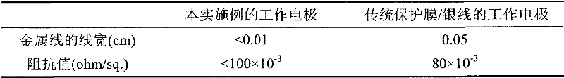
由表1的数据可知,本实施例的工作电极的阻抗值与传统具保护膜/银线的工作电极的阻抗值相去不远,但就金属线的线宽而言,本实施例的金属线宽显著小于传统保护膜/银线的线宽。因此,本实施例的金属线层,不仅没有与电解质产生反应的风险,更具有较小的线宽,可减少金属线遮盖导电基板的程度。也因此,本发明的金属线层可具有更密实的金属线以提供更好的电子传导效率,而不至于影响导电基板的透光度。As can be seen from the data in Table 1, the impedance value of the working electrode of the present embodiment is not far from the impedance value of the working electrode of the traditional protective film/silver wire, but in terms of the line width of the metal wire, the metal wire of the present embodiment The width is significantly smaller than the line width of traditional protective film/silver lines. Therefore, the metal line layer of this embodiment not only has no risk of reacting with the electrolyte, but also has a smaller line width, which can reduce the extent to which the metal line covers the conductive substrate. Therefore, the metal wire layer of the present invention can have denser metal wires to provide better electron conduction efficiency without affecting the light transmittance of the conductive substrate.
实施例二:制备具本发明的金属线层的对电极Embodiment 2: Preparation of the counter electrode with the metal wire layer of the present invention
请参阅图3A,选用具可挠性的聚萘二甲酸乙二醇酯(PEN)作为本实施例工作电极(阳极)310的导电基板311的基材312,将铟锡氧化物(ITO,Indium Tin Oxide)以溅镀的方式于前述基材的表面形成一导电层313。然后以蒸镀的方式将钛金属布植于前述导电层313之上以形成本实施例的金属线层314。前述金属线层314的形状如图3B所示,为并行线状,以维持对电极(阴极)310良好的透光度。Please refer to Fig. 3A, select flexible polyethylene naphthalate (PEN) as the
接着以真空镀膜的方式于设有前述金属线层314的前述导电层313的表面覆盖一铂层,作为触媒层315(厚度为1nm),便完成本实施例的对电极(阴极)310。Then, a platinum layer is covered on the surface of the
实施例三:制备本发明的电化学装置Embodiment 3: Preparation of the electrochemical device of the present invention
请参阅图4,以染料敏化太阳能电池400为本实施例电化学装置的例子,其各层体结构分述如下:Please refer to FIG. 4, taking the dye-sensitized
选用具可挠性的钛板(Ti)作为本实施例工作电极(阳极)410的导电基板411,接着再将二氧化钛纳米颗粒(TiO2)涂布于其上,以制得厚度约为15μm的TiO2/Ti电极。接着将前述TiO2/Ti光电极裁切为面积8公分×8公分(长×宽)的大小后,置于电热炉中以500℃烧结30分钟,以强化二氧化钛纳米颗粒之间的连接力。然后于室温下,将TiO2/Ti光电极浸泡于0.3mmol/L的光激发染料溶液(将0.036克的N719染料溶于100毫升叔丁醇与乙腈混合液中,其中乙腈∶叔丁醇的体积比为1∶1)中12小时,使光激发染料充分吸附于二氧化钛纳米颗粒的表面。最后,再以乙腈清洗,以获得感光层412,而完成本实施例的工作电极(阳极)410。由于钛为导电性良好的物质,因此本实施例的工作电极410不需要设置金属线层。A flexible titanium plate (Ti) is selected as the
对电极(阴极)420:使用实施例二所述的对电极。简述之,其包含由基材422和导电层423所构成的导电基板421;由金属钛所构成的第二金属线层424;及触媒层425。Counter electrode (cathode) 420: use the counter electrode described in Embodiment 2. Briefly, it includes a
电解质430为含碘及碘离子的有机溶液,更明确地,为溶于乙腈(acetonitrile)的0.6mol/L的1-丁基-3-甲基-碘化咪唑铵(BMImI)、0.1mol/L的碘化锂(LiI)、0.05mol/L的碘(I2)、0.05mol/L的4-叔丁基吡啶(4-tert-butylpyridine,TBP)和0.1M的硫氰酸胍(guanidinium thiocyanate,GuSCN)。The
组装:使用SX-1170-25热塑膜(Solaronix)作为封装材料(图中未示),将该热塑膜置于前述工作电极410和前述对电极420之间,加热至约100℃并施予适当压力使前述工作电极410和前述对电极420分别与热塑膜粘合,接着将前述电解质430灌入并充满于前述热塑膜与前述工作电极410和前述对电极420所形成的内部空间,便完成含有本发明的染料敏化太阳能电池400。Assembly: use SX-1170-25 thermoplastic film (Solaronix) as packaging material (not shown in the figure), place the thermoplastic film between the aforementioned working
所属领域的技术人员当可了解,在不违背本发明精神下,依据本案实施方式所能进行的各种变化。因此,显见所列的实施方式并非用以限制本发明,而是企图在所附权利要求保护范围的定义下,涵盖于本发明的精神与范畴中所做的修改。Those skilled in the art should be able to understand various changes that can be made according to the embodiments of the present invention without departing from the spirit of the present invention. Therefore, it is obvious that the listed embodiments are not intended to limit the present invention, but are intended to cover modifications made within the spirit and scope of the present invention within the definition of the scope of protection of the appended claims.
以上所述的具体实施例,对本发明的目的、技术方案和有益效果进行了进一步详细说明,所应理解的是,以上所述仅为本发明的具体实施例而已,并不用于限定本发明的保护范围,凡在本发明的精神和原则之内,所做的任何修改、等同替换、改进等,均应包含在本发明的保护范围之内。The specific embodiments described above have further described the purpose, technical solutions and beneficial effects of the present invention in detail. It should be understood that the above descriptions are only specific embodiments of the present invention and are not intended to limit the scope of the present invention. Protection scope, within the spirit and principles of the present invention, any modification, equivalent replacement, improvement, etc., shall be included in the protection scope of the present invention.
Claims (19)
Priority Applications (1)
| Application Number | Priority Date | Filing Date | Title |
|---|---|---|---|
| CN 201010180990 CN102243921A (en) | 2010-05-14 | 2010-05-14 | Dye-sensitized solar cell with metal wire layer and electrode thereof |
Applications Claiming Priority (1)
| Application Number | Priority Date | Filing Date | Title |
|---|---|---|---|
| CN 201010180990 CN102243921A (en) | 2010-05-14 | 2010-05-14 | Dye-sensitized solar cell with metal wire layer and electrode thereof |
Publications (1)
| Publication Number | Publication Date |
|---|---|
| CN102243921A true CN102243921A (en) | 2011-11-16 |
Family
ID=44961923
Family Applications (1)
| Application Number | Title | Priority Date | Filing Date |
|---|---|---|---|
| CN 201010180990 Pending CN102243921A (en) | 2010-05-14 | 2010-05-14 | Dye-sensitized solar cell with metal wire layer and electrode thereof |
Country Status (1)
| Country | Link |
|---|---|
| CN (1) | CN102243921A (en) |
Cited By (5)
| Publication number | Priority date | Publication date | Assignee | Title |
|---|---|---|---|---|
| CN104616900A (en) * | 2015-01-23 | 2015-05-13 | 三峡大学 | Cobalt-nickel metal sulfide, preparation method and application thereof |
| CN104733182A (en) * | 2013-12-20 | 2015-06-24 | 深圳富泰宏精密工业有限公司 | Solar cell panel and manufacturing method thereof |
| CN105070510A (en) * | 2015-08-26 | 2015-11-18 | 长江大学 | Flexible dye-sensitized solar cell and preparation method thereof |
| CN106544693A (en) * | 2016-11-28 | 2017-03-29 | 北京工业大学 | A kind of preparation of multilevel hierarchy ZnO@CoS membrane electrodes and its application in photoelectric decomposition water |
| CN106663546A (en) * | 2014-11-12 | 2017-05-10 | 株式会社藤仓 | Electrolyte for dye-sensitized photoelectric conversion elements for low luminance, and dye-sensitized photoelectric conversion element for low luminance using same |
Citations (3)
| Publication number | Priority date | Publication date | Assignee | Title |
|---|---|---|---|---|
| US20060112988A1 (en) * | 2003-01-15 | 2006-06-01 | Masahiro Morooka | Photoelectric conversion element |
| CN101002292A (en) * | 2004-08-11 | 2007-07-18 | 戴索有限公司 | Photoelectrochemical photovoltaic panel and method to manufacture thereof |
| JP2010050039A (en) * | 2008-08-25 | 2010-03-04 | Fujimori Kogyo Co Ltd | Photoelectrode substrate for dye-sensitized solar battery and dye-sensitized solar battery using the same |
-
2010
- 2010-05-14 CN CN 201010180990 patent/CN102243921A/en active Pending
Patent Citations (3)
| Publication number | Priority date | Publication date | Assignee | Title |
|---|---|---|---|---|
| US20060112988A1 (en) * | 2003-01-15 | 2006-06-01 | Masahiro Morooka | Photoelectric conversion element |
| CN101002292A (en) * | 2004-08-11 | 2007-07-18 | 戴索有限公司 | Photoelectrochemical photovoltaic panel and method to manufacture thereof |
| JP2010050039A (en) * | 2008-08-25 | 2010-03-04 | Fujimori Kogyo Co Ltd | Photoelectrode substrate for dye-sensitized solar battery and dye-sensitized solar battery using the same |
Cited By (7)
| Publication number | Priority date | Publication date | Assignee | Title |
|---|---|---|---|---|
| CN104733182A (en) * | 2013-12-20 | 2015-06-24 | 深圳富泰宏精密工业有限公司 | Solar cell panel and manufacturing method thereof |
| CN106663546A (en) * | 2014-11-12 | 2017-05-10 | 株式会社藤仓 | Electrolyte for dye-sensitized photoelectric conversion elements for low luminance, and dye-sensitized photoelectric conversion element for low luminance using same |
| CN106663546B (en) * | 2014-11-12 | 2018-07-13 | 株式会社藤仓 | The electrolyte of low-light (level) dye-sensitized photoelectric conversion element and the low-light (level) dye-sensitized photoelectric conversion element for using the electrolyte |
| CN104616900A (en) * | 2015-01-23 | 2015-05-13 | 三峡大学 | Cobalt-nickel metal sulfide, preparation method and application thereof |
| CN104616900B (en) * | 2015-01-23 | 2017-11-10 | 三峡大学 | A kind of cobalt nickel bimetal sulfide, preparation method and applications |
| CN105070510A (en) * | 2015-08-26 | 2015-11-18 | 长江大学 | Flexible dye-sensitized solar cell and preparation method thereof |
| CN106544693A (en) * | 2016-11-28 | 2017-03-29 | 北京工业大学 | A kind of preparation of multilevel hierarchy ZnO@CoS membrane electrodes and its application in photoelectric decomposition water |
Similar Documents
| Publication | Publication Date | Title |
|---|---|---|
| JP5300735B2 (en) | Dye-sensitized solar cell module | |
| Brown et al. | Progress in flexible dye solar cell materials, processes and devices | |
| Chiu et al. | High efficiency flexible dye-sensitized solar cells by multiple electrophoretic depositions | |
| KR20100091883A (en) | Dye-sensitized photoelectric conversion device module and method for manufacturing the same, photoelectric conversion device module and method for manufacturing the same, and electronic device | |
| Cha et al. | Dye-sensitized solar cells on glass paper: TCO-free highly bendable dye-sensitized solar cells inspired by the traditional Korean door structure | |
| JPWO2011096154A1 (en) | Dye-sensitized solar cell and method for producing the same | |
| KR100384893B1 (en) | Nano-particle oxide solar cells and fabrication method of the same and solar cell modules and transparent electric window using the same | |
| Wu et al. | Electrochemical formation of transparent nanostructured TiO 2 film as an effective bifunctional layer for dye-sensitized solar cells | |
| CN102243921A (en) | Dye-sensitized solar cell with metal wire layer and electrode thereof | |
| CN102074376A (en) | Dye-sensitized solar battery | |
| JP5134867B2 (en) | Photoelectric conversion element | |
| TWI481040B (en) | Working electrode, method for fabricating the same and dye-sensitized solar cell containing the same | |
| Moon et al. | Titanium oxide films prepared by sputtering, sol gel and dip coating methods for photovoltaic application | |
| JP5128118B2 (en) | Wet solar cell and manufacturing method thereof | |
| CN103531362A (en) | High-efficiency flexible dye-sensitized solar cell and preparation method thereof | |
| ur Rehman et al. | Conventional versus Flexible Substrates for Dye Sensitized and Perovskite Type Photo Voltaic Solar Cells | |
| JP6773859B1 (en) | Electrolyte for photoelectric conversion element and photoelectric conversion element | |
| JP4841574B2 (en) | Dye-sensitized solar cell module and manufacturing method thereof | |
| JP5160045B2 (en) | Photoelectric conversion element | |
| CN102243923A (en) | Dye-sensitized solar cell with dewatering mechanism | |
| JP2012156070A (en) | Method for forming photocatalyst film in dye-sensitized solar battery, and dye-sensitized solar battery | |
| KR101156585B1 (en) | Dye-sensitized sollar cell and its fabrication method | |
| KR101321645B1 (en) | Dye solar cell with silane coupling co-adsorbent and method of manufacturing the same | |
| WO2014132725A1 (en) | Dye-sensitized solar cell | |
| KR101407894B1 (en) | Dye solar cell with chemically bonded co-adsorbent and method of manufacturing the same |
Legal Events
| Date | Code | Title | Description |
|---|---|---|---|
| C06 | Publication | ||
| PB01 | Publication | ||
| C10 | Entry into substantive examination | ||
| SE01 | Entry into force of request for substantive examination | ||
| C02 | Deemed withdrawal of patent application after publication (patent law 2001) | ||
| WD01 | Invention patent application deemed withdrawn after publication |
Application publication date: 20111116 |