[go: up one dir, main page]

CN102222764B - Method for manufacturing phase change memory - Google Patents

Method for manufacturing phase change memory Download PDF

Info

Publication number
CN102222764B
CN102222764B CN201110172980XA CN201110172980A CN102222764B CN 102222764 B CN102222764 B CN 102222764B CN 201110172980X A CN201110172980X A CN 201110172980XA CN 201110172980 A CN201110172980 A CN 201110172980A CN 102222764 B CN102222764 B CN 102222764B
Authority
CN
China
Prior art keywords
carbon nanotube
phase change
layer
nanotube layer
electrode leads
Prior art date
Legal status (The legal status is an assumption and is not a legal conclusion. Google has not performed a legal analysis and makes no representation as to the accuracy of the status listed.)
Active
Application number
CN201110172980XA
Other languages
Chinese (zh)
Other versions
CN102222764A (en
Inventor
柳鹏
李群庆
姜开利
范守善
Current Assignee (The listed assignees may be inaccurate. Google has not performed a legal analysis and makes no representation or warranty as to the accuracy of the list.)
Tsinghua University
Hongfujin Precision Industry Shenzhen Co Ltd
Original Assignee
Tsinghua University
Hongfujin Precision Industry Shenzhen Co Ltd
Priority date (The priority date is an assumption and is not a legal conclusion. Google has not performed a legal analysis and makes no representation as to the accuracy of the date listed.)
Filing date
Publication date
Application filed by Tsinghua University, Hongfujin Precision Industry Shenzhen Co Ltd filed Critical Tsinghua University
Priority to CN201110172980XA priority Critical patent/CN102222764B/en
Priority to TW100126510A priority patent/TWI492372B/en
Publication of CN102222764A publication Critical patent/CN102222764A/en
Priority to US13/332,486 priority patent/US8621746B2/en
Application granted granted Critical
Publication of CN102222764B publication Critical patent/CN102222764B/en
Active legal-status Critical Current
Anticipated expiration legal-status Critical

Links

Images

Classifications

    • HELECTRICITY
    • H10SEMICONDUCTOR DEVICES; ELECTRIC SOLID-STATE DEVICES NOT OTHERWISE PROVIDED FOR
    • H10NELECTRIC SOLID-STATE DEVICES NOT OTHERWISE PROVIDED FOR
    • H10N70/00Solid-state devices having no potential barriers, and specially adapted for rectifying, amplifying, oscillating or switching
    • H10N70/20Multistable switching devices, e.g. memristors
    • H10N70/231Multistable switching devices, e.g. memristors based on solid-state phase change, e.g. between amorphous and crystalline phases, Ovshinsky effect
    • HELECTRICITY
    • H10SEMICONDUCTOR DEVICES; ELECTRIC SOLID-STATE DEVICES NOT OTHERWISE PROVIDED FOR
    • H10NELECTRIC SOLID-STATE DEVICES NOT OTHERWISE PROVIDED FOR
    • H10N70/00Solid-state devices having no potential barriers, and specially adapted for rectifying, amplifying, oscillating or switching
    • H10N70/801Constructional details of multistable switching devices
    • H10N70/841Electrodes
    • H10N70/8413Electrodes adapted for resistive heating
    • HELECTRICITY
    • H10SEMICONDUCTOR DEVICES; ELECTRIC SOLID-STATE DEVICES NOT OTHERWISE PROVIDED FOR
    • H10NELECTRIC SOLID-STATE DEVICES NOT OTHERWISE PROVIDED FOR
    • H10N70/00Solid-state devices having no potential barriers, and specially adapted for rectifying, amplifying, oscillating or switching
    • H10N70/801Constructional details of multistable switching devices
    • H10N70/881Switching materials
    • H10N70/882Compounds of sulfur, selenium or tellurium, e.g. chalcogenides
    • H10N70/8828Tellurides, e.g. GeSbTe
    • YGENERAL TAGGING OF NEW TECHNOLOGICAL DEVELOPMENTS; GENERAL TAGGING OF CROSS-SECTIONAL TECHNOLOGIES SPANNING OVER SEVERAL SECTIONS OF THE IPC; TECHNICAL SUBJECTS COVERED BY FORMER USPC CROSS-REFERENCE ART COLLECTIONS [XRACs] AND DIGESTS
    • Y10TECHNICAL SUBJECTS COVERED BY FORMER USPC
    • Y10TTECHNICAL SUBJECTS COVERED BY FORMER US CLASSIFICATION
    • Y10T29/00Metal working
    • Y10T29/49Method of mechanical manufacture
    • Y10T29/49002Electrical device making
    • Y10T29/49117Conductor or circuit manufacturing
    • Y10T29/49124On flat or curved insulated base, e.g., printed circuit, etc.
    • Y10T29/49126Assembling bases
    • YGENERAL TAGGING OF NEW TECHNOLOGICAL DEVELOPMENTS; GENERAL TAGGING OF CROSS-SECTIONAL TECHNOLOGIES SPANNING OVER SEVERAL SECTIONS OF THE IPC; TECHNICAL SUBJECTS COVERED BY FORMER USPC CROSS-REFERENCE ART COLLECTIONS [XRACs] AND DIGESTS
    • Y10TECHNICAL SUBJECTS COVERED BY FORMER USPC
    • Y10TTECHNICAL SUBJECTS COVERED BY FORMER US CLASSIFICATION
    • Y10T29/00Metal working
    • Y10T29/49Method of mechanical manufacture
    • Y10T29/49002Electrical device making
    • Y10T29/49117Conductor or circuit manufacturing
    • Y10T29/49124On flat or curved insulated base, e.g., printed circuit, etc.
    • Y10T29/4913Assembling to base an electrical component, e.g., capacitor, etc.

Landscapes

  • Semiconductor Memories (AREA)

Abstract

The invention provides a method for manufacturing a phase change memory, comprising the following steps: providing a substrate; forming a first line of electrode leads and a second line of electrode leads, wherein the first line of electrode leads and the second line of electrode leads are spaced apart on one surface of the substrate; providing a carbon nano tube layer which is in an integrally continuous layer structure; laying the carbon nano tube layer on the surface of the substrate directly and contacting the carbon nano tube layer with the second line of electrode leads; arranging a phase change layer on one surface of the carbon nano tube layer; and arranging a first row of electrode leads and a second row of electrode leads, wherein the first row of electrode leads and the second row of electrode leads are spaced apart on the surface of the substrate and isolated from and intersected with the first line of electrode leads and the second line of electrode leads, the second row of electrode leads is contacted with the phase change layer, a first electrode is arranged in a mode of contacting with the first line of electrode leads and the carbon nano tube layer, and a second electrode is arranged in a mode of contacting with the first row of electrode leads and the carbon nano tube layer.

Description

相变存储器的制备方法Preparation method of phase change memory

技术领域technical field

本发明涉及一种相变存储器的制备方法,尤其是涉及一种具有碳纳米管的相变存储器的制备方法。The invention relates to a preparation method of a phase-change memory, in particular to a preparation method of a phase-change memory with carbon nanotubes.

背景技术Background technique

存储器是信息产业中重要的组成部件之一,如何发展新型的低成本、高密度、速度快、长寿命的非易失存储器一直是信息产业研究的重要方向。Memory is one of the important components in the information industry. How to develop a new low-cost, high-density, fast-speed, and long-life non-volatile memory has always been an important direction of information industry research.

作为非易失性存储器的下一代产品,相变存储器是一种利用特殊相变材料的晶相与非晶相导电性的差异来存储信息的存储器,通过一加热器件加热相变层使之在晶相与非晶相之间进行转换来存储信息。相变存储器基于其独特的特点如较快的响应速度、较优的耐用性以及较长的数据保存时间等,已备受关注,其不仅能够在移动电话、数码相机、MP3播放器、移动存储卡等民用微电子领域得到广泛应用,而且在航空航天及导弹系统等军用领域有着重要的应用前景。相变存储器主要通过一加热器件加热相变层实现数据的存储。现有技术中,相变存储器中的加热器件通过在一基底的表面溅射或蒸镀一介质层的方法形成,工艺复杂且制备成本相对较高。As the next-generation product of non-volatile memory, phase-change memory is a memory that uses the difference in conductivity between the crystalline phase and the amorphous phase of a special phase-change material to store information. A heating device heats the phase-change layer to make it Switching between crystalline and amorphous phases is used to store information. Based on its unique characteristics such as faster response speed, better durability and longer data storage time, phase change memory has attracted much attention. It can not only be used in mobile phones, digital cameras, MP3 players, mobile storage Cards and other civil microelectronics are widely used, and have important application prospects in military fields such as aerospace and missile systems. The phase change memory mainly realizes data storage by heating the phase change layer through a heating device. In the prior art, the heating device in the phase-change memory is formed by sputtering or vapor-depositing a dielectric layer on the surface of a substrate, and the process is complicated and the manufacturing cost is relatively high.

发明内容Contents of the invention

有鉴于此,确有必要提供一种工艺简单、成本较低的相变存储器的制备方法。In view of this, it is indeed necessary to provide a method for preparing a phase change memory with simple process and low cost.

一种相变存储器的制备方法,其包括以下步骤:提供一基底;在所述基底一表面形成多个第一行电极引线及多个第二行电极引线;在所述设置有第一行电极引线及第二行电极引线的基底的表面设置一碳纳米管层;图案化处理所述碳纳米管层,形成多个分散的碳纳米管层单元;在每一碳纳米管层单元的表面设置一相变层;在所述基底的表面设置多个第一电极、多个第二电极、多个第一列电极引线及多个第二列电极引线,所述每一第一电极接触连接所述第一行电极引线与每一碳纳米管层单元,所述每一第二电极接触连接所述第一列电极引线与每一碳纳米管层单元,第二列电极引线与所述每一相变层接触设置。A method for preparing a phase change memory, comprising the following steps: providing a substrate; forming a plurality of first row electrode leads and a plurality of second row electrode leads on a surface of the substrate; A carbon nanotube layer is arranged on the surface of the base of the lead wire and the second row of electrode leads; the carbon nanotube layer is patterned to form a plurality of dispersed carbon nanotube layer units; the surface of each carbon nanotube layer unit is arranged A phase change layer; a plurality of first electrodes, a plurality of second electrodes, a plurality of first column electrode leads and a plurality of second column electrode leads are arranged on the surface of the substrate, and each of the first electrodes is contacted and connected to the The electrode leads of the first row are connected to each carbon nanotube layer unit, and each second electrode is connected to the electrode leads of the first row and each carbon nanotube layer unit, and the electrode leads of the second row are connected to each carbon nanotube layer unit. Phase change layer contact setup.

相较于现有技术,本发明提供的相变存储器的制备方法,通过将碳纳米管层直接铺设在所述基底的表面制备所述加热器件,制备方法简单,成本较低。Compared with the prior art, in the preparation method of the phase change memory provided by the present invention, the heating device is prepared by laying the carbon nanotube layer directly on the surface of the substrate, and the preparation method is simple and the cost is low.

附图说明Description of drawings

图1为本发明第一实施例提供的相变存储单元的俯视示意图。FIG. 1 is a schematic top view of a phase-change memory cell provided by a first embodiment of the present invention.

图2为本发明第一实施例提供的相变存储单元中碳纳米管膜的电子扫描电镜照片。FIG. 2 is a scanning electron micrograph of the carbon nanotube film in the phase change memory unit provided by the first embodiment of the present invention.

图3为本发明第一实施例提供的相变存储单元的制备方法的工艺流程图。FIG. 3 is a process flow chart of a method for manufacturing a phase-change memory cell according to the first embodiment of the present invention.

图4为本发明第二实施例提供的相变存储单元的俯视示意图。FIG. 4 is a schematic top view of a phase-change memory cell provided by a second embodiment of the present invention.

图5为图4所示的相变存储器沿线V-V的剖面示意图。FIG. 5 is a schematic cross-sectional view of the phase change memory shown in FIG. 4 along the line V-V.

图6为本发明第二实施例提供的相变存储单元的制备方法的工艺流程图。FIG. 6 is a process flow chart of a method for manufacturing a phase-change memory cell according to the second embodiment of the present invention.

图7为本发明第三实施例提供的相变存储单元的俯视示意图。FIG. 7 is a schematic top view of a phase-change memory cell provided by a third embodiment of the present invention.

图8为图7所示的相变存储器沿线Ⅷ-VⅢ的剖面示意图。FIG. 8 is a schematic cross-sectional view of the phase change memory shown in FIG. 7 along the line VIII-VIII.

图9为本发明第三实施例提供的具有双层相变层的相变存储单元的结构示意图。FIG. 9 is a schematic structural diagram of a phase change memory cell with double phase change layers according to the third embodiment of the present invention.

图10为图9所示的相变存储器沿线X-X的剖面示意图。FIG. 10 is a schematic cross-sectional view of the phase change memory shown in FIG. 9 along line X-X.

图11为本发明第四实施例提供的相变存储器的俯视示意图。FIG. 11 is a schematic top view of a phase-change memory provided by a fourth embodiment of the present invention.

图12为本发明第四实施例提供的相变存储器的制备方法的工艺流程图。主要元件符号说明FIG. 12 is a process flow diagram of a manufacturing method of a phase-change memory according to a fourth embodiment of the present invention. Description of main component symbols

相变存储单元            10,20,30Phase Change Memory Unit 10,20,30

基底                    100Base 100

碳纳米管层              110carbon nanotube layer 110

相变层                  120Phase change layer 120

第一电极                132First electrode 132

第二电极                134Second electrode 134

第三电极               136The third electrode 136

第四电极               138Fourth electrode 138

第一行电极引线         142The first row of electrode leads 142

第二行电极引线         144Second row electrode leads 144

第一列电极引线         146The first row of electrode leads 146

第二列电极引线         148Second column electrode leads 148

绝缘层                 101Insulation layer 101

网格                   102Grid 102

相变存储结构           104Phase Change Storage Structure 104

相变存储器             40Phase change memory 40

如下具体实施方式将结合上述附图进一步说明本发明。The following specific embodiments will further illustrate the present invention in conjunction with the above-mentioned drawings.

具体实施方式Detailed ways

以下将结合附图对本发明的相变存储器及其制备方法作进一步的详细说明。为便于理解,本发明首先对所述相变存储器的相变存储单元及其制备方法做详细描述。The phase change memory and its preparation method of the present invention will be further described in detail below in conjunction with the accompanying drawings. For ease of understanding, the present invention firstly describes the phase change memory unit of the phase change memory and its preparation method in detail.

请参阅图1,本发明第一实施例提供一种相变存储单元10,其包括一基底100、至少一碳纳米管层110、至少一相变层120、一第一电极132、一第二电极134、一第三电极136及一第四电极138。所述基底100用于支撑所述碳纳米管层110、所述相变层120、所述第一电极132、所述第二电极134及所述第三电极136。所述碳纳米管层110与所述相变层120层叠设置。所述相变存储单元10包括一数据写入电路,所述数据写入电路依次串联所述第一电极132、所述碳纳米管层110及第二电极134电连接,所述数据写入电路用于相变存储单元10的数据写入;一数据读取电路,所述数据读取电路包括依次串联的第三电极136、至少一相变层120及一第四电极138;所述第三电极136与所述相变层120电连接,所述数据读取电路用于相变存储单元10工作过程中的数据读取。所述至少一相变层120与所述碳纳米管层110至少部分重叠设置。1, the first embodiment of the present invention provides a phase change memory unit 10, which includes a substrate 100, at least one carbon nanotube layer 110, at least one phase change layer 120, a first electrode 132, a second The electrode 134 , a third electrode 136 and a fourth electrode 138 . The substrate 100 is used to support the carbon nanotube layer 110 , the phase change layer 120 , the first electrode 132 , the second electrode 134 and the third electrode 136 . The carbon nanotube layer 110 is stacked with the phase change layer 120 . The phase-change memory unit 10 includes a data writing circuit, and the data writing circuit sequentially connects the first electrode 132, the carbon nanotube layer 110 and the second electrode 134 in series, and the data writing circuit It is used for data writing of the phase change memory cell 10; a data read circuit, the data read circuit includes a third electrode 136, at least one phase change layer 120 and a fourth electrode 138 connected in series; the third The electrode 136 is electrically connected to the phase change layer 120 , and the data reading circuit is used for reading data during the operation of the phase change memory unit 10 . The at least one phase change layer 120 is at least partially overlapped with the carbon nanotube layer 110 .

所述基底100为一绝缘基板,如陶瓷基板、玻璃基板、树脂基板、石英基板等,优选的,所述基底100具有耐高温的特性,以适应相变存储单元10工作过程中所需的温度而保持其几何形状基本不变。所述基底100的大小与厚度不限,本领域技术人员可以根据所述相变存储单元10需要的工作温度进行选择。优选的,所述基底100为一柔性基板,其材料可为聚酰亚胺、酚醛树脂、聚酯树脂、聚酰胺树脂等。本实施例中,所述基底100的材料为聚酰亚胺,其厚度为20微米,在400摄氏度时仍可保持其几何形状不变。The base 100 is an insulating substrate, such as a ceramic substrate, a glass substrate, a resin substrate, a quartz substrate, etc., preferably, the base 100 has high temperature resistance characteristics, so as to adapt to the temperature required during the operation of the phase change memory unit 10 And keep its geometric shape basically unchanged. The size and thickness of the substrate 100 are not limited, those skilled in the art can select according to the required working temperature of the phase change memory unit 10 . Preferably, the base 100 is a flexible substrate, and its material can be polyimide, phenolic resin, polyester resin, polyamide resin and the like. In this embodiment, the material of the base 100 is polyimide, the thickness of which is 20 microns, and its geometric shape can still be maintained at 400 degrees Celsius.

所述碳纳米管层110的平面形状可为三角形、方形、矩形、圆形、椭圆形或其他几何形状,所述碳纳米管层110的尺寸不限。所述碳纳米管层110的平面形状及尺寸可以根据相变存储单元10的形状及尺寸等实际需要进行选择。本实施例中,所述碳纳米管层110的形状为矩形,所述矩形的长可为50纳米~900微米,宽可为20纳米~600微米,本实施例中所述矩形的长为70微米、宽为50微米。所述碳纳米管层110的厚度可为0.5纳米~100微米,优选的,所述碳纳米管层110的厚度为5微米~20微米。The planar shape of the carbon nanotube layer 110 can be triangular, square, rectangular, circular, oval or other geometric shapes, and the size of the carbon nanotube layer 110 is not limited. The planar shape and size of the carbon nanotube layer 110 can be selected according to actual requirements such as the shape and size of the phase change memory unit 10 . In this embodiment, the shape of the carbon nanotube layer 110 is a rectangle, the length of the rectangle can be 50 nanometers to 900 microns, and the width can be 20 nanometers to 600 microns, and the length of the rectangle in this embodiment is 70. Microns, 50 microns wide. The carbon nanotube layer 110 may have a thickness of 0.5 nanometers to 100 micrometers, preferably, the carbon nanotube layer 110 may have a thickness of 5 micrometers to 20 micrometers.

所述碳纳米管层110包括多个碳纳米管,所述多个碳纳米管的延伸方向基本平行于所述碳纳米管层表面。当所述碳纳米管层110设置于所述基底100表面时,所述碳纳米管层110中的碳纳米管的延伸方向平行于所述基底100的表面延伸。具体的,所述碳纳米管层110为一连续的膜状结构或线状结构,所述碳纳米管层110中的多个碳纳米管可无序排列或有序排列。所谓无序排列是指碳纳米管的排列方向无规则。所谓有序排列是指碳纳米管的排列方向有规则。具体地,当碳纳米管层110包括无序排列的碳纳米管时,所述碳纳米管相互缠绕或者各向同性排列;当碳纳米管层110包括有序排列的碳纳米管时,所述碳纳米管沿一个方向或者多个方向择优取向延伸。所谓“择优取向”是指所述碳纳米管层110中的大多数碳纳米管在一个方向上具有较大的取向几率;即,该碳纳米管层110中的大多数碳纳米管的轴向基本沿同一方向延伸。The carbon nanotube layer 110 includes a plurality of carbon nanotubes, and the extension direction of the plurality of carbon nanotubes is substantially parallel to the surface of the carbon nanotube layer. When the carbon nanotube layer 110 is disposed on the surface of the substrate 100 , the carbon nanotubes in the carbon nanotube layer 110 extend parallel to the surface of the substrate 100 . Specifically, the carbon nanotube layer 110 is a continuous film-like structure or a linear structure, and a plurality of carbon nanotubes in the carbon nanotube layer 110 can be arranged randomly or in an orderly manner. The so-called disordered arrangement means that the arrangement direction of the carbon nanotubes is irregular. The so-called ordered arrangement means that the arrangement direction of the carbon nanotubes is regular. Specifically, when the carbon nanotube layer 110 includes disorderly arranged carbon nanotubes, the carbon nanotubes are intertwined or arranged isotropically; when the carbon nanotube layer 110 includes ordered arranged carbon nanotubes, the Carbon nanotubes extend in one direction or in multiple directions with preferred orientation. The so-called "preferred orientation" means that most of the carbon nanotubes in the carbon nanotube layer 110 have a greater orientation probability in one direction; that is, the axial direction of most of the carbon nanotubes in the carbon nanotube layer 110 Basically extend in the same direction.

具体地,所述碳纳米管层110包括至少一碳纳米管膜、至少一碳纳米管线或至少一碳纳米管膜与至少一碳纳米管线的组合。所述碳纳米管膜或碳纳米管线为多个碳纳米管组成的自支撑结构,所述多个碳纳米管通过范德华力(van der Waals force)相连。所述自支撑是指碳纳米管层110不需要大面积的载体支撑,而只要相对两边提供支撑力即能整体上悬空而保持自身状态,即将该碳纳米管层110置于(或固定于)间隔一定距离设置的两个支撑体上时,位于两个支撑体之间的碳纳米管碾压膜能够悬空保持自身状态。所述自支撑主要通过碳纳米管碾压膜中存在连续的通过范德华力相连延伸的碳纳米管而实现。进一步的,所述碳纳米管层110未经过任何化学修饰或功能化处理。Specifically, the carbon nanotube layer 110 includes at least one carbon nanotube film, at least one carbon nanotube wire, or a combination of at least one carbon nanotube film and at least one carbon nanotube wire. The carbon nanotube film or carbon nanotube wire is a self-supporting structure composed of a plurality of carbon nanotubes, and the plurality of carbon nanotubes are connected by van der Waals force. The self-supporting means that the carbon nanotube layer 110 does not need a large-area carrier support, but as long as the supporting force is provided on the opposite sides, it can be suspended as a whole and maintain its own state, that is, the carbon nanotube layer 110 is placed (or fixed) on When the two support bodies are arranged at a certain distance, the carbon nanotube rolling film located between the two support bodies can be suspended in the air and maintain its own state. The self-supporting is mainly realized by the presence of continuous carbon nanotubes connected and extended by van der Waals force in the carbon nanotube rolling film. Further, the carbon nanotube layer 110 has not undergone any chemical modification or functionalization treatment.

所述碳纳米管膜可以为碳纳米管拉膜、碳纳米管碾压膜和碳纳米管絮化膜,所述碳纳米管线可为一非扭转的碳纳米管线或扭转的碳纳米管线,本实施例中所述碳纳米管层110为碳纳米管拉膜。The carbon nanotube film can be a carbon nanotube drawn film, a carbon nanotube rolled film, and a carbon nanotube flocculated film, and the carbon nanotube line can be a non-twisted carbon nanotube line or a twisted carbon nanotube line. The carbon nanotube layer 110 in the embodiment is a carbon nanotube drawn film.

请参阅图2,所述碳纳米管拉膜是由若干碳纳米管组成的自支撑结构。所述若干碳纳米管沿同一方向择优取向延伸。该碳纳米管拉膜中大多数碳纳米管的整体延伸方向基本朝同一方向。而且,所述大多数碳纳米管的整体延伸方向基本平行于碳纳米管拉膜的表面。进一步地,所述碳纳米管拉膜中多数碳纳米管是通过范德华力首尾相连。具体地,所述碳纳米管拉膜中基本朝同一方向延伸的大多数碳纳米管中每一碳纳米管与在延伸方向上相邻的碳纳米管通过范德华力首尾相连。当然,所述碳纳米管拉膜中存在少数随机排列的碳纳米管,这些碳纳米管不会对碳纳米管拉膜中大多数碳纳米管的整体取向排列构成明显影响。所述碳纳米管拉膜中基本朝同一方向延伸的多数碳纳米管,并非绝对的直线状,可以适当的弯曲;或者并非完全按照延伸方向上排列,可以适当的偏离延伸方向。因此,不能排除碳纳米管拉膜的基本朝同一方向延伸的多数碳纳米管中并列的碳纳米管之间可能存在部分接触。Please refer to FIG. 2 , the carbon nanotube drawn film is a self-supporting structure composed of several carbon nanotubes. The plurality of carbon nanotubes preferably extend along the same direction. The overall extension direction of most carbon nanotubes in the carbon nanotube drawn film basically faces the same direction. Moreover, the overall extension direction of most of the carbon nanotubes is substantially parallel to the surface of the drawn carbon nanotube film. Further, most of the carbon nanotubes in the carbon nanotube drawn film are connected end to end by van der Waals force. Specifically, each carbon nanotube in the majority of carbon nanotubes extending in the same direction in the drawn carbon nanotube film is connected end-to-end with the adjacent carbon nanotubes in the extending direction through van der Waals force. Of course, there are a few randomly arranged carbon nanotubes in the drawn carbon nanotube film, and these carbon nanotubes will not significantly affect the overall alignment of most carbon nanotubes in the drawn carbon nanotube film. Most of the carbon nanotubes extending in the same direction in the drawn carbon nanotube film are not absolutely straight and can be properly bent; or they are not completely arranged in the extending direction and can be appropriately deviated from the extending direction. Therefore, it cannot be ruled out that there may be partial contact between the parallel carbon nanotubes among the carbon nanotubes extending in the same direction in the drawn carbon nanotube film.

所述碳纳米管拉膜包括多个连续且定向排列的碳纳米管片段。该若干碳纳米管片段通过范德华力首尾相连。每一碳纳米管片段包括多个相互平行的碳纳米管,该多个相互平行的碳纳米管通过范德华力紧密结合。该碳纳米管片段具有任意的长度、厚度、均匀性及形状。该碳纳米管拉膜中的碳纳米管沿同一方向择优取向延伸。所述碳纳米管拉膜的结构及其制备方法请参见2010年5月26日公告的,公告号为CN101239712B的中国发明专利说明书。The carbon nanotube stretched film includes a plurality of continuous and aligned carbon nanotube segments. The several carbon nanotube segments are connected end to end by van der Waals force. Each carbon nanotube segment includes a plurality of parallel carbon nanotubes, and the plurality of parallel carbon nanotubes are closely combined by van der Waals force. The carbon nanotube segment has any length, thickness, uniformity and shape. The carbon nanotubes in the carbon nanotube stretched film preferably extend along the same direction. For the structure and preparation method of the carbon nanotube stretched film, please refer to the Chinese invention patent specification with the announcement number CN101239712B announced on May 26, 2010.

当所述碳纳米管层110包括多个碳纳米管膜时,该多个碳纳米管膜可层叠设置形成一体结构,相邻两层碳纳米管膜之间通过范德华力紧密结合。优选的,当所述碳纳米管膜为拉膜时,所述相邻两层碳纳米管膜中碳纳米管的择优取向延伸方向形成一夹角α,其中0°≤α≤90°。当α=0°时,所述相邻两层碳纳米管膜可称之为彼此同向设置;当0°<α≤90°时,所述相邻两层碳纳米管膜可称之为彼此交叉设置。所述多层碳纳米管膜层叠设置可以提高其强度,碳纳米管层110工作过程中可更好的保持其形状和结构。优选的,所述碳纳米管层110包括多个交叉排列的多层碳纳米管膜,可进一步增强其机械强度。When the carbon nanotube layer 110 includes a plurality of carbon nanotube films, the plurality of carbon nanotube films can be stacked to form an integrated structure, and two adjacent layers of carbon nanotube films are tightly bonded by van der Waals force. Preferably, when the carbon nanotube film is a stretched film, the preferred orientation extension directions of the carbon nanotubes in the two adjacent carbon nanotube films form an included angle α, where 0°≤α≤90°. When α=0°, the two adjacent layers of carbon nanotube films can be said to be arranged in the same direction as each other; when 0°<α≤90°, the two adjacent layers of carbon nanotube films can be called set across each other. The stacked arrangement of the multi-layer carbon nanotube film can improve its strength, and the shape and structure of the carbon nanotube layer 110 can be better maintained during the working process. Preferably, the carbon nanotube layer 110 includes a plurality of cross-arranged multilayer carbon nanotube films, which can further enhance its mechanical strength.

所述碳纳米管碾压膜包括均匀分布的碳纳米管,该碳纳米管各向同性,沿同一方向或不同方向择优取向排列。优选地,所述碳纳米管碾压膜中的碳纳米管平行于碳纳米管碾压膜的表面。所述碳纳米管碾压膜中的碳纳米管相互交叠。所述碳纳米管碾压膜中碳纳米管之间通过范德华力相互吸引,紧密结合,使得该碳纳米管碾压膜具有很好的柔韧性,可以弯曲折叠成任意形状而不破裂。且由于碳纳米管碾压膜中的碳纳米管之间通过范德华力相互吸引,紧密结合,使碳纳米管碾压膜为一自支撑的结构,可无需基底支撑,自支撑存在。所述碳纳米管碾压膜可通过碾压一碳纳米管阵列获得。所述碳纳米管碾压膜中的碳纳米管与形成碳纳米管阵列的基体的表面形成一夹角α,其中,α大于等于0度且小于等于15度(0≤α≤15°),该夹角α与施加在碳纳米管阵列上的压力有关,压力越大,该夹角越小。所述碳纳米管碾压膜的长度和宽度不限。The carbon nanotube rolling film includes uniformly distributed carbon nanotubes, the carbon nanotubes are isotropic, and are preferentially oriented in the same direction or in different directions. Preferably, the carbon nanotubes in the carbon nanotube rolled film are parallel to the surface of the carbon nanotube rolled film. The carbon nanotubes in the carbon nanotube rolled film overlap each other. The carbon nanotubes in the carbon nanotube rolling film are attracted to each other by van der Waals force and are closely combined, so that the carbon nanotube rolling film has good flexibility and can be bent and folded into any shape without breaking. Moreover, because the carbon nanotubes in the carbon nanotube rolling film are attracted to each other by van der Waals force and are tightly combined, the carbon nanotube rolling film is a self-supporting structure, which can exist without the support of the substrate. The carbon nanotube rolled film can be obtained by rolling a carbon nanotube array. The carbon nanotubes in the carbon nanotube rolling film form an angle α with the surface of the substrate forming the carbon nanotube array, where α is greater than or equal to 0 degrees and less than or equal to 15 degrees (0≤α≤15°), The included angle α is related to the pressure exerted on the carbon nanotube array, the greater the pressure, the smaller the included angle. The length and width of the carbon nanotube rolled film are not limited.

所述碳纳米管絮化膜包括相互缠绕的碳纳米管,所述碳纳米管膜中碳纳米管的长度大于10微米。所述碳纳米管之间通过范德华力相互吸引、缠绕,形成网络状结构。所述碳纳米管絮化膜膜各向同性。所述碳纳米管絮化膜中的碳纳米管为均匀分布,无规则排列,形成大量的微孔结构,微孔孔径大约小于10微米。所述碳纳米管絮化膜的长度和宽度不限。The carbon nanotube flocculation film includes intertwined carbon nanotubes, and the length of the carbon nanotubes in the carbon nanotube film is greater than 10 microns. The carbon nanotubes attract and entangle with each other through van der Waals force to form a network structure. The carbon nanotube flocculation film is isotropic. The carbon nanotubes in the carbon nanotube flocculation film are evenly distributed and randomly arranged, forming a large number of microporous structures, and the diameter of the micropores is about less than 10 microns. The length and width of the carbon nanotube flocculated film are not limited.

所述相变层120与所述碳纳米管层110至少部分层叠设置,所述“层叠设置”是指所述碳纳米管层110为自支撑的层状结构,所述相变层120的表面与所述碳纳米管层110的表面彼此平行且接触设置,且所述相变层120与所述碳纳米管层110中的碳纳米管的延伸方向平行设置。本实施例中,所述相变层120的至少部分表面与所述碳纳米管层110的部分表面接触设置。进一步的,在所述相变层120与所述碳纳米管层110之间可进一步包括一导热层(图未示),所述导热层用于将碳纳米管层110产生的热量传导给所述相变层;所述导热层的材料可为金、银、铜等,也可为其他导热材料,可根据实际需要进行选择。进一步的,所述相变层120也可与所述碳纳米管层110之间存在一定间隔,只要保证所述碳纳米管层110产生的热量能够使所述相变层120发生相变即可。所述相变层120的厚度可为10纳米~200纳米,其形状可为三角形、方形、矩形、圆形、椭圆形或其他几何形状。优选地,相变层120设置在碳纳米管层110的范围内,即所述相变层120的面积小于所述碳纳米管层110的面积,且所述相变层120整体位于所述碳纳米管层110覆盖的范围内。本实施例中,所述相变层120的形状为圆形,其直径为20纳米~250微米。所述相变层120的材料可为锗锑碲、锗碲、硅锑碲、硅碲或硫系化合物等相变材料,所述相变材料在碳纳米管层110加热过程中,相变材料的温度发生改变时可在晶相和非晶相之间进行可逆转换。本实施例中,所述相变材料为锗锑碲,其初始状态为高阻态的非晶相,其由高阻态的非晶相转变为低阻态的晶相的相变温度为200~300摄氏度;由晶相转变为非晶相的复位温度为400~500摄氏度。The phase change layer 120 and the carbon nanotube layer 110 are at least partially stacked. The "stacked" means that the carbon nanotube layer 110 is a self-supporting layered structure, and the surface of the phase change layer 120 The surfaces of the carbon nanotube layer 110 are arranged parallel to and in contact with each other, and the phase change layer 120 is arranged parallel to the extending direction of the carbon nanotubes in the carbon nanotube layer 110 . In this embodiment, at least part of the surface of the phase change layer 120 is disposed in contact with part of the surface of the carbon nanotube layer 110 . Further, a heat conduction layer (not shown) may be further included between the phase change layer 120 and the carbon nanotube layer 110, and the heat conduction layer is used to conduct heat generated by the carbon nanotube layer 110 to the carbon nanotube layer 110. The phase-change layer; the material of the heat-conducting layer can be gold, silver, copper, etc., or other heat-conducting materials, which can be selected according to actual needs. Further, there may be a certain distance between the phase change layer 120 and the carbon nanotube layer 110, as long as the heat generated by the carbon nanotube layer 110 can make the phase change layer 120 undergo a phase change. . The thickness of the phase change layer 120 may be 10 nm to 200 nm, and its shape may be triangular, square, rectangular, circular, elliptical or other geometric shapes. Preferably, the phase change layer 120 is arranged within the scope of the carbon nanotube layer 110, that is, the area of the phase change layer 120 is smaller than the area of the carbon nanotube layer 110, and the phase change layer 120 is entirely located on the carbon nanotube layer 110. within the range covered by the nanotube layer 110. In this embodiment, the shape of the phase change layer 120 is circular, and its diameter is 20 nanometers to 250 micrometers. The material of the phase change layer 120 can be a phase change material such as germanium antimony tellurium, germanium tellurium tellurium, silicon antimony tellurium, silicon tellurium or a chalcogenide compound. A reversible switch between crystalline and amorphous phases occurs when the temperature is changed. In this embodiment, the phase change material is germanium antimony tellurium, its initial state is a high-resistance amorphous phase, and its phase transition temperature from a high-resistance amorphous phase to a low-resistance crystalline phase is 200 ~300 degrees Celsius; the reset temperature for changing from crystal phase to amorphous phase is 400~500 degrees Celsius.

所述第一电极132、第二电极134的材料可分别为导电材料制成的导电体,如金属层、ITO层等,所述第一电极132、第二电极134的厚度可为10纳米~100微米,优选的为20纳米~50纳米。优选的,本实施例中所述第一电极132与第二电极134的材料为导电浆料,该导电浆料的成分包括金属粉、低熔点玻璃粉和粘结剂;其中,该金属粉优选为银粉,该粘结剂优选为松油醇或乙基纤维素。该导电浆料中,金属粉的重量比为50~90%,低熔点玻璃粉的重量比为2~10%,粘结剂的重量比为8~40%。所述第一电极132与第二电极134分别可通过丝网印刷法印制于所述碳纳米管层110的部分表面。所述第一电极132与第二电极134的形状、大小及设置位置不限,只要保证所述第一电极132及第二电极134之间施加电压时,能够使所述碳纳米管层110加热到所述相变层120的相变温度即可。优选的,所述第一电极132与第二电极134相对设置于所述碳纳米管层110的两端,且分别与碳纳米管层110相对两端的每一根碳纳米管电连接,从而与所述碳纳米管层110整体电连接,使所述碳纳米管层110中的电流可均匀分布,提高碳纳米管层110的发热效率。The materials of the first electrode 132 and the second electrode 134 can be conductors made of conductive materials, such as metal layers, ITO layers, etc., and the thickness of the first electrode 132 and the second electrode 134 can be 10 nanometers to 10 nanometers. 100 micrometers, preferably 20 nanometers to 50 nanometers. Preferably, the materials of the first electrode 132 and the second electrode 134 in this embodiment are conductive paste, and the components of the conductive paste include metal powder, low-melting glass powder and binder; wherein, the metal powder is preferably is silver powder, the binder is preferably terpineol or ethyl cellulose. In the conductive paste, the weight ratio of the metal powder is 50-90%, the weight ratio of the low-melting glass powder is 2-10%, and the weight ratio of the binder is 8-40%. The first electrode 132 and the second electrode 134 can be printed on part of the surface of the carbon nanotube layer 110 by screen printing. The shape, size and setting position of the first electrode 132 and the second electrode 134 are not limited, as long as the voltage is applied between the first electrode 132 and the second electrode 134, the carbon nanotube layer 110 can be heated. It only needs to reach the phase transition temperature of the phase transition layer 120 . Preferably, the first electrode 132 and the second electrode 134 are disposed opposite to the two ends of the carbon nanotube layer 110, and are respectively electrically connected to each carbon nanotube at the opposite ends of the carbon nanotube layer 110, so as to be connected to the carbon nanotube layer 110. The carbon nanotube layer 110 is electrically connected as a whole, so that the current in the carbon nanotube layer 110 can be evenly distributed, and the heating efficiency of the carbon nanotube layer 110 is improved.

所述第三电极136及所述第四电极138分别与所述相变层120电接触设置。本实施例中,所述第三电极136、第四电极138部分覆盖于所述相变层120的表面。具体的,所述相变层120设置于第三电极136、第四电极138与碳纳米管层110之间,通过在第三电极136与第四电极138之间施加一电压,进而在所述相变层120中通入一电流。进一步的,所述第四电极138也可以设置仅与所述碳纳米管层110电连接设置,此时也可用第一电极132、第二电极134替代,即也可在第三电极136与第一电极132之间施加电压或第三电极136与第二电极134之间施加电压,所述第三电极136、相变层120、碳纳米管层110以及第一电极132或者第二电极134依次串联形成一导电通路。所述第三电极136及第四电极138的形状及尺寸不限,可根据实际需要进行选择。所述第三电极136、第四电极138的材料可与所述第一电极132相同或者不同。本实施例中,所述第三电极136、第四电极138的材料也分别为导电浆料。The third electrode 136 and the fourth electrode 138 are respectively disposed in electrical contact with the phase change layer 120 . In this embodiment, the third electrode 136 and the fourth electrode 138 partially cover the surface of the phase change layer 120 . Specifically, the phase change layer 120 is disposed between the third electrode 136, the fourth electrode 138 and the carbon nanotube layer 110, and by applying a voltage between the third electrode 136 and the fourth electrode 138, the A current is passed through the phase change layer 120 . Further, the fourth electrode 138 can also be set only to be electrically connected to the carbon nanotube layer 110, at this time, it can also be replaced by the first electrode 132 and the second electrode 134, that is, the third electrode 136 can also be connected to the second electrode 136. A voltage is applied between an electrode 132 or a voltage is applied between the third electrode 136 and the second electrode 134, and the third electrode 136, the phase change layer 120, the carbon nanotube layer 110, and the first electrode 132 or the second electrode 134 are sequentially connected in series to form a conductive path. The shape and size of the third electrode 136 and the fourth electrode 138 are not limited, and can be selected according to actual needs. The material of the third electrode 136 and the fourth electrode 138 may be the same as or different from that of the first electrode 132 . In this embodiment, the materials of the third electrode 136 and the fourth electrode 138 are also conductive paste.

所述相变存储单元10的工作过程分为三个:数据写入、数据读取、数据复位。初始状态下相变层120为非晶相,电阻率较高,代表数据“0”;而晶相的相变层120电阻率较低代表数据“1”。所述相变存储单元10写入数据时,在所述第一电极132与第二电极134之间输入一电信号,使所述碳纳米管层110产生热量,进而加热与所述碳纳米管层110接触的所述相变层120并使之达到相变温度,使所述相变层120中的相变材料由高阻态的非晶相转变为低阻态的晶相,并且使所述相变层120由高阻态变为低阻并维持,完成数据的写入;在读取数据时,在所述第三电极136与第四电极138之间,或在第三电极136与第一电极132之间、或第三电极136与第二电极134之间施加一电压从而输入一电信号,所述电信号的电流较弱,不会引起所述相变层120的相变,但通过测量电路中的电流大小,即可得出相变层120的电阻,并与初始状态时相变层120的电阻相比较,当得到的相变层120电阻小于初始状态的电阻时,读取数据“1”;当得到的电阻与初始状态的电阻相等时,读取数据“0”;在复位相变存储单元10时,在碳纳米管层110中通入一窄而强的脉冲电流,使之迅速产生较多的热量,所述热量使所述相变层120由晶相转变为非晶相,完成相变存储单元10的数据复位过程。The working process of the phase-change memory cell 10 is divided into three steps: data writing, data reading, and data resetting. In the initial state, the phase change layer 120 is in an amorphous phase with a high resistivity, which represents data "0"; while the phase change layer 120 in a crystalline phase has a low resistivity, which represents data "1". When the phase-change memory unit 10 writes data, an electrical signal is input between the first electrode 132 and the second electrode 134, so that the carbon nanotube layer 110 generates heat, and then heats the carbon nanotube layer 110. Layer 110 contacts the phase change layer 120 and makes it reach the phase transition temperature, so that the phase change material in the phase change layer 120 changes from a high-resistance amorphous phase to a low-resistance crystalline phase, and makes all The phase-change layer 120 changes from a high-resistance state to a low-resistance state and maintains it to complete the writing of data; when reading data, between the third electrode 136 and the fourth electrode 138, or between the third electrode 136 and the fourth electrode 138 A voltage is applied between the first electrodes 132, or between the third electrode 136 and the second electrode 134 to input an electrical signal, the current of the electrical signal is relatively weak and will not cause the phase change of the phase change layer 120, However, by measuring the magnitude of the current in the circuit, the resistance of the phase change layer 120 can be obtained, and compared with the resistance of the phase change layer 120 in the initial state, when the obtained resistance of the phase change layer 120 is less than the resistance of the initial state, read Take the data "1"; when the obtained resistance is equal to the resistance of the initial state, read the data "0"; when resetting the phase change memory unit 10, pass a narrow and strong pulse current in the carbon nanotube layer 110 , so that it quickly generates more heat, and the heat causes the phase change layer 120 to change from a crystalline phase to an amorphous phase, and completes the data reset process of the phase change memory unit 10 .

请参阅图3,本实施例进一步提供所述相变存储单元10的制备方法,其主要包括以下步骤:Please refer to FIG. 3 , this embodiment further provides a method for preparing the phase-change memory cell 10, which mainly includes the following steps:

步骤S11,提供一基底100;Step S11, providing a substrate 100;

步骤S12,在所述基底100一表面层叠设置一碳纳米管层110及一相变层120;Step S12, stacking a carbon nanotube layer 110 and a phase change layer 120 on a surface of the substrate 100;

步骤S13,在所述碳纳米管层110表面间隔设置一第一电极132、一第二电极134以及在所述相变层120的表面,间隔设置一第三电极136、一第四电极138。Step S13 , disposing a first electrode 132 and a second electrode 134 on the surface of the carbon nanotube layer 110 at intervals, and disposing a third electrode 136 and a fourth electrode 138 on the surface of the phase change layer 120 at intervals.

在步骤S12中,所述碳纳米管层110包括多个碳纳米管,所述多个碳纳米管的延伸方向基本平行于所述碳纳米管层表面。所述碳纳米管层110中的碳纳米管的延伸方向平行于所述基底100的表面延伸。所述碳纳米管层110为一连续的自支撑结构,从而所述碳纳米管层110可通过直接铺设的方法设置。本实施例中,所述碳纳米管层110设置于基底100的表面,所述相变层120设置于该碳纳米管层110远离基底100的表面。所述相变层120可通过电子束沉积、离子束沉积、化学气相沉积或磁控溅射的方法形成在所述碳纳米管层110表面。本实施例中,所述相变层120通过磁控溅射方法形成在所述碳纳米管层110的表面。In step S12, the carbon nanotube layer 110 includes a plurality of carbon nanotubes, and the extension direction of the plurality of carbon nanotubes is substantially parallel to the surface of the carbon nanotube layer. The extension direction of the carbon nanotubes in the carbon nanotube layer 110 is parallel to the surface of the substrate 100 . The carbon nanotube layer 110 is a continuous self-supporting structure, so the carbon nanotube layer 110 can be installed by a direct laying method. In this embodiment, the carbon nanotube layer 110 is disposed on the surface of the substrate 100 , and the phase change layer 120 is disposed on the surface of the carbon nanotube layer 110 away from the substrate 100 . The phase change layer 120 can be formed on the surface of the carbon nanotube layer 110 by electron beam deposition, ion beam deposition, chemical vapor deposition or magnetron sputtering. In this embodiment, the phase change layer 120 is formed on the surface of the carbon nanotube layer 110 by magnetron sputtering.

在步骤S13中,所述第一电极132、第二电极134、第三电极136及第四电极可通过丝网印刷、离子束沉积、电子束沉积、镀膜等方法中的任意一种或多种制备。本实施例中,所述第一电极132、第二电极134、所述第三电极及第四电阻分别通过丝网印刷法设置。具体的,所述第一电极132与第二电极134设置于所述碳纳米管层110相对的两端,并且彼此间隔设置。所述第三电极136、第四电极138间隔设置于该相变层120远离基底100的表面,所述第三电极136、第四电极138与碳纳米管层110之间间隔设置有相变层120。In step S13, the first electrode 132, the second electrode 134, the third electrode 136 and the fourth electrode can be formed by any one or more methods of screen printing, ion beam deposition, electron beam deposition, coating, etc. preparation. In this embodiment, the first electrode 132 , the second electrode 134 , the third electrode and the fourth resistor are respectively provided by screen printing. Specifically, the first electrode 132 and the second electrode 134 are disposed at two opposite ends of the carbon nanotube layer 110 and are spaced apart from each other. The third electrode 136 and the fourth electrode 138 are arranged at intervals on the surface of the phase change layer 120 away from the substrate 100, and the phase change layer is arranged at intervals between the third electrode 136, the fourth electrode 138 and the carbon nanotube layer 110 120.

本实施例提供的相变存储单元的制备方法,由于所述碳纳米管层为一自支撑的结构,因此可以直接铺设于所述基底的表面作为相变层的加热器件,制备工艺简单,并且所述碳纳米管层与所述相变层层叠设置,因此可以提高所述相变存储单元的机械强度,提高加热效率。In the preparation method of the phase change memory unit provided in this embodiment, since the carbon nanotube layer is a self-supporting structure, it can be directly laid on the surface of the substrate as a heating device for the phase change layer, the preparation process is simple, and The carbon nanotube layer is stacked with the phase change layer, so the mechanical strength of the phase change memory unit can be improved, and the heating efficiency can be improved.

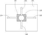
请参阅图4及图5,本发明第二实施例提供一种相变存储单元20,其包括一基底100、一碳纳米管层110、一相变层120、一第一电极132、一第二电极134、一第一行电极引线142、一第二行电极引线144、一第一列电极引线146及一第二列电极引线148。所述相变存储单元20具有一第一电路及一第二电路设置于所述基底100表面,所述第一电路包括第一行电极引线142、第一电极132、碳纳米管层110、第一列电极引线146依次串联形成一导电通路,所述第一电路用于相变存储单元20工作过程中的数据写入。所述第二电路包括至少部分层叠设置的碳纳米管层110、相变层120串联于第二行电极引线144与第二列电极引线148之间形成一导电通路,所述第二电路用于相变存储单元20工作过程中的数据读取。所述第一电路及第二电路均可用于相变存储单元20工作过程中的数据复位。4 and 5, the second embodiment of the present invention provides a phase-change memory unit 20, which includes a substrate 100, a carbon nanotube layer 110, a phase-change layer 120, a first electrode 132, a first Two electrodes 134 , a first row electrode lead 142 , a second row electrode lead 144 , a first column electrode lead 146 and a second column electrode lead 148 . The phase change memory unit 20 has a first circuit and a second circuit disposed on the surface of the substrate 100, the first circuit includes a first row electrode lead 142, a first electrode 132, a carbon nanotube layer 110, a second A row of electrode leads 146 are sequentially connected in series to form a conductive path, and the first circuit is used for data writing in the phase change memory cell 20 during operation. The second circuit includes at least partially stacked carbon nanotube layers 110, and the phase change layer 120 is connected in series between the second row electrode lead 144 and the second column electrode lead 148 to form a conductive path. The second circuit is used for Data reading during the working process of the phase change memory unit 20 . Both the first circuit and the second circuit can be used for data reset during the working process of the phase change memory unit 20 .

具体的,所述第一行电极引线142与第二行电极引线144平行且间隔设置于所述基底100上,所述第一列电极引线146与第二列电极引线148平行且间隔设置于所述基底100上,并且所述第一行电极引线142与第一列电极引线146、第二列电极引线148相互交叉且间隔设置,所述第二行电极引线144分别与第一列电极引线146、第二列电极引线148相互交叉且间隔设置。所述相变层120、碳纳米管层110层叠设置于所述第二行电极引线144与第二列电极引线148的交叉处。所述第一列电极引线146、所述第二电极134、所述碳纳米管层110、所述第一电极132与第一行电极引线142依序电连接在一外部电源之间形成所述第一电路,所述第一电路构成一加热回路用于加热所述相变层120从而写入数据。所述第二行电极引线144、碳纳米管层110、相变层120、第二列电极引线148依序连接形成所述第二电路,所述第二电路构成数据读取回路用于测量相变层120的电阻,从而读取数据。当在所述第一行电极引线142与所述第一列电极引线146之间加载一电压时,电流从所述第一行电极引线142经由所述碳纳米管层110流入所述第一列电极引线146;所述第二行电极引线144与所述第二列电极引线148之间加载一电压时,电流从所述第二行电极引线144经由所述碳纳米管层110和所述相变层120流入所述第二列电极引线148。Specifically, the first row electrode leads 142 and the second row electrode leads 144 are parallel and spaced apart on the substrate 100, and the first column electrode leads 146 and the second column electrode leads 148 are parallel and spaced apart on the substrate 100. On the substrate 100, and the first row electrode leads 142, the first column electrode leads 146, and the second column electrode leads 148 intersect each other and are arranged at intervals, and the second row electrode leads 144 are connected to the first column electrode leads 146 respectively. , The electrode leads 148 of the second row intersect with each other and are arranged at intervals. The phase change layer 120 and the carbon nanotube layer 110 are stacked at the intersection of the second row electrode lead 144 and the second column electrode lead 148 . The first column electrode lead 146, the second electrode 134, the carbon nanotube layer 110, the first electrode 132 and the first row electrode lead 142 are electrically connected in sequence between an external power supply to form the A first circuit, the first circuit constitutes a heating circuit for heating the phase change layer 120 to write data. The second row electrode leads 144, the carbon nanotube layer 110, the phase change layer 120, and the second column electrode leads 148 are sequentially connected to form the second circuit, and the second circuit constitutes a data reading loop for measuring phase The resistance of layer 120 is varied, thereby reading data. When a voltage is applied between the first row electrode lead 142 and the first column electrode lead 146, current flows from the first row electrode lead 142 through the carbon nanotube layer 110 into the first column electrode lead 146; when a voltage is applied between the second row electrode lead 144 and the second column electrode lead 148, the current passes from the second row electrode lead 144 through the carbon nanotube layer 110 and the phase The variable layer 120 flows into the second column electrode lead 148 .

所述第一行电极引线142与第二行电极引线144彼此平行且间隔设置,所述第一行电极引线142与第二行电极引线144的间距为50纳米~2厘米,该第一行电极引线142与第二行电极引线144的宽度分别为30纳米~100微米,厚度分别为10纳米~100纳米。所述第一行电极引线142、第二行电极引线144为导电材料制成的导电体,如金属层、ITO层等,优选的,本实施例中所述第一行电极引线142、第二行电极引线144的材料为导电浆料。所述第一行电极引线142、第二行电极引线144可通过丝网印刷法印制于所述绝缘基底100上。可以理解,所述第一行电极引线142与第二行电极引线144的材料不限,只要是导电的材料均可。The first row electrode leads 142 and the second row electrode leads 144 are arranged parallel to each other and at intervals, the distance between the first row electrode leads 142 and the second row electrode leads 144 is 50 nanometers to 2 centimeters, the first row electrodes The widths of the lead wires 142 and the second row electrode lead wires 144 are respectively 30 nm to 100 microns, and the thicknesses are respectively 10 nm to 100 nm. The first row electrode leads 142 and the second row electrode leads 144 are conductors made of conductive materials, such as metal layers, ITO layers, etc. Preferably, the first row electrode leads 142 and the second row electrode leads 142 in this embodiment The material of the row electrode lead 144 is conductive paste. The first row electrode leads 142 and the second row electrode leads 144 can be printed on the insulating substrate 100 by screen printing. It can be understood that the materials of the first row electrode leads 142 and the second row electrode leads 144 are not limited, as long as they are conductive materials.

所述第一列电极引线146与第二列电极引线148彼此平行且间隔设置于基底100上。所述第一列电极引线146分别与第一行电极引线142、第二行电极引线144交叉设置,并在交叉处通过一绝缘层101绝缘设置。所述绝缘层101的材料不限,如SiO2、Si3N4、Ta2O5等,所述绝缘层101的厚度可为50纳米~200纳米,可根据实际需要进行选择。该第一列电极引线146与第一行电极引线142、第二行电极引线144的交叉角度分别为10度到90度,优选为90度,即该第一列电极引线146与第一行电极引线142、第二行电极引线144相互垂直。The first row electrode leads 146 and the second row electrode leads 148 are arranged parallel to each other and spaced apart on the substrate 100 . The first column electrode leads 146 are respectively intersected with the first row electrode leads 142 and the second row electrode leads 144 , and are insulated by an insulating layer 101 at the intersections. The material of the insulating layer 101 is not limited, such as SiO 2 , Si 3 N 4 , Ta 2 O 5 , etc. The thickness of the insulating layer 101 may be 50 nm to 200 nm, which can be selected according to actual needs. The intersection angles of the first column electrode leads 146 and the first row electrode leads 142 and the second row electrode leads 144 are respectively 10 degrees to 90 degrees, preferably 90 degrees, that is, the first column electrode leads 146 and the first row electrodes The lead wires 142 and the second row electrode lead wires 144 are perpendicular to each other.

同样的,所述第二列电极引线148也分别与第一行电极引线142、第二行电极引线144相互垂直交叉设置,且所述第二列电极引线148与第一行电极引线142的交叉位置处设置有绝缘层101。所述第二列电极引线148与第二行电极引线144的交叉位置处层叠设置有一碳纳米管层110及相变层120使所述第二列电极引线148与第二行电极引线144间隔。Similarly, the second column electrode leads 148 are vertically crossed with the first row electrode leads 142 and the second row electrode leads 144 respectively, and the intersection of the second column electrode leads 148 and the first row electrode leads 142 An insulating layer 101 is provided at the position. A carbon nanotube layer 110 and a phase change layer 120 are stacked at the intersection of the second row electrode lead 148 and the second row electrode lead 144 to separate the second row electrode lead 148 from the second row electrode lead 144 .

具体的,所述碳纳米管层110设置于所述第二行电极引线144与第二列电极引线148的交叉处,并覆盖部分第二行电极引线144且与其电连接。进一步的,所述碳纳米管层110与所述第二行电极引线144之间的部分表面可包括一绝缘层(图未示),所述绝缘层没有将所述碳纳米管层110与所述第二行电极引线144完全绝缘开,所述绝缘层用以减少所述碳纳米管层110与所述第二行电极引线144之间的接触面积,从而使所述加热电流尽量的从碳纳米管中流过以加热所述碳纳米管层110。所述所述碳纳米管层110的形状可为三角形、方形、矩形、圆形、椭圆形或其他几何形状,所述碳纳米管层110的尺寸不限。本实施例中,所述碳纳米管的形状为矩形,所述矩形的长可为50纳米~900微米,宽可为20纳米~600微米,本实施例中所述矩形的长为70微米、宽为50微米。所述碳纳米管层110的厚度可为0.5纳米~100微米,优选的,所述碳纳米管层110的厚度为5微米~20微米。本实施例中,所述碳纳米管层110可通过将一碳纳米管膜平铺在所述基底100上,然后利用光刻、电子刻蚀或等离子刻蚀等方法对所述碳纳米管膜进行处理,以保留必需的部分,形成所需的图案。Specifically, the carbon nanotube layer 110 is disposed at the intersection of the second row electrode lead 144 and the second column electrode lead 148 , covers part of the second row electrode lead 144 and is electrically connected thereto. Further, part of the surface between the carbon nanotube layer 110 and the second row electrode lead 144 may include an insulating layer (not shown in the figure), and the insulating layer does not separate the carbon nanotube layer 110 from the second row of electrode leads 144. The second row electrode leads 144 are completely insulated, and the insulating layer is used to reduce the contact area between the carbon nanotube layer 110 and the second row electrode leads 144, so that the heating current is as far as possible from the carbon The nanotubes flow through to heat the carbon nanotube layer 110 . The shape of the carbon nanotube layer 110 can be triangular, square, rectangular, circular, oval or other geometric shapes, and the size of the carbon nanotube layer 110 is not limited. In this embodiment, the shape of the carbon nanotubes is a rectangle, the length of the rectangle can be 50 nanometers to 900 microns, and the width can be 20 nanometers to 600 microns, and the length of the rectangle in this embodiment is 70 microns, 50 microns wide. The carbon nanotube layer 110 may have a thickness of 0.5 nanometers to 100 micrometers, preferably, the carbon nanotube layer 110 may have a thickness of 5 micrometers to 20 micrometers. In this embodiment, the carbon nanotube layer 110 can be formed by laying a carbon nanotube film on the substrate 100, and then using photolithography, electronic etching or plasma etching to remove the carbon nanotube film. Processing is performed to preserve the necessary portions to form the desired pattern.

所述相变层120可与所述碳纳米管层110层叠设置,本实施例中,所述相变层120的一表面与所述碳纳米管层110的一表面接触设置。进一步的,所述相变层120与所述碳纳米管层110之间可进一步包括一导热层(图未示),用于将碳纳米管层110产生的热量传导给所述相变层120。所述相变层120的厚度可为10纳米~200纳米,其形状可为三角形、方形、矩形、圆形、椭圆形或其他几何形状。本实施例中,所述相变层120的形状为圆形,其直径为50微米~250微米。所述相变层120的材料可为锗锑碲、锗碲、硅锑碲、硅碲或硫系化合物等相变材料,所述相变材料在碳纳米管层110加热过程中,温度发生改变时可在晶相和非晶相之间进行可逆转换,本实施例中,所述相变材料为锗锑碲,其相变温度为200~300摄氏度。The phase change layer 120 can be stacked with the carbon nanotube layer 110 . In this embodiment, one surface of the phase change layer 120 is in contact with one surface of the carbon nanotube layer 110 . Further, a heat conduction layer (not shown) may be further included between the phase change layer 120 and the carbon nanotube layer 110 for conducting the heat generated by the carbon nanotube layer 110 to the phase change layer 120 . The thickness of the phase change layer 120 may be 10 nm to 200 nm, and its shape may be triangular, square, rectangular, circular, elliptical or other geometric shapes. In this embodiment, the shape of the phase change layer 120 is circular, and its diameter is 50 micrometers to 250 micrometers. The material of the phase change layer 120 can be a phase change material such as germanium antimony tellurium, germanium tellurium tellurium, silicon antimony tellurium, silicon tellurium or a chalcogenide compound, and the temperature of the phase change material changes during the heating process of the carbon nanotube layer 110 The reversible transformation between the crystalline phase and the amorphous phase can be carried out at the same time. In this embodiment, the phase change material is germanium antimony tellurium, and its phase change temperature is 200-300 degrees Celsius.

进一步的,在所述碳纳米管层110及相变层120远离基底的表面及周围可设置一绝缘隔热材料(图未示),所述绝缘隔热材料将所述碳纳米管层110及相变层120裸露于基底100的表面包覆。所述绝缘隔热材料可通过涂覆、丝网印刷等方法形成在所述碳纳米管层110及相变层120的表面。所述绝缘隔热材料用于减少碳纳米管层110在对相变层120加热过程热量的损失,使得所述相变层120快速的达到相变温度而发生相变,提高所述相变存储单元20的响应速度。Further, an insulating and heat-insulating material (not shown) may be provided on and around the surface of the carbon nanotube layer 110 and the phase-change layer 120 away from the substrate, and the insulating and heat-insulating material connects the carbon nanotube layer 110 and the The phase change layer 120 is exposed to cover the surface of the substrate 100 . The insulating and heat insulating material can be formed on the surface of the carbon nanotube layer 110 and the phase change layer 120 by methods such as coating and screen printing. The insulating heat insulating material is used to reduce the heat loss of the carbon nanotube layer 110 during the heating process of the phase change layer 120, so that the phase change layer 120 quickly reaches the phase change temperature and undergoes a phase change, improving the storage capacity of the phase change. The response speed of the unit 20.

所述第一电极132为条形电极,由所述第一行电极引线142向所述第二行电极引线144延伸,具体的,所述第一电极132的延伸方向垂直于所述第一行电极引线142。所述第一电极132一端部设置于所述第一行电极引线142上并电连接,另一端部与所述碳纳米管层110接触。所述第一电极132的结构和材料可与所述第一行电极引线142相同。本实施例中,所述第一电极132平行于所述第二列电极引线148且相互间隔设置。进一步的,所述第一电极132与所述第二行电极引线144之间设置有绝缘层101。可以理解,所述第一电极132为一可选择的结构,即所述第一行电极引线142也可直接与所述碳纳米管层110电连接。The first electrode 132 is a strip electrode, extending from the first row electrode lead 142 to the second row electrode lead 144, specifically, the extension direction of the first electrode 132 is perpendicular to the first row electrode leads 142 . One end of the first electrode 132 is disposed on the first row electrode lead 142 and electrically connected, and the other end is in contact with the carbon nanotube layer 110 . The structure and material of the first electrode 132 may be the same as that of the first row electrode lead 142 . In this embodiment, the first electrodes 132 are arranged parallel to the second column electrode leads 148 and spaced apart from each other. Further, an insulating layer 101 is disposed between the first electrode 132 and the second row electrode lead 144 . It can be understood that the first electrode 132 is an optional structure, that is, the first row electrode lead 142 can also be directly electrically connected to the carbon nanotube layer 110 .

所述第二电极134为条形电极,由所述第一列电极引线146向所述第二列电极引线148延伸,具体的,所述第二电极134的延伸方向平行于所述第一行电极引线142。所述第二电极134的一端与所述第一列电极引线146连接,另一端与所述碳纳米管层110接触。所述第二电极134的结构和材料可与所述第一行电极引线142相同。所述第二电极134与所述碳纳米管层110电连接而不接触所述第一电极132,从而所述第一电极132、第二电极134以及碳纳米管层110形成一闭合的工作电路,并使碳纳米管层110与所述第一列电极引线146电连接形成第一电路用于写入数据。可以理解,所述第二电极134为一可选择的结构,即所述第一列电极引线146也可直接与所述碳纳米管层110电连接。The second electrode 134 is a strip electrode, extending from the first column electrode lead 146 to the second column electrode lead 148, specifically, the extension direction of the second electrode 134 is parallel to the first row electrode leads 142 . One end of the second electrode 134 is connected to the first column electrode lead 146 , and the other end is in contact with the carbon nanotube layer 110 . The structure and material of the second electrode 134 may be the same as that of the first row electrode lead 142 . The second electrode 134 is electrically connected to the carbon nanotube layer 110 without contacting the first electrode 132, so that the first electrode 132, the second electrode 134 and the carbon nanotube layer 110 form a closed working circuit , and electrically connect the carbon nanotube layer 110 to the first column electrode lead 146 to form a first circuit for writing data. It can be understood that the second electrode 134 is an optional structure, that is, the electrode leads 146 of the first column can also be directly electrically connected to the carbon nanotube layer 110 .

所述相变存储单元20工作时,所述第一行电极引线142作为相变存储单元20的写行电极,所述第二行电极引线144作为读行电极,所述第一列电极引线146作为写列电极,所述第二列电极引线148作为读列电极。在写入数据时,在所述写行电极及写列电极中输入一电信号,通过第一电极132及第二电极134在第一电路中通入电流,使所述碳纳米管层110产生热量,进而加热所述初始状态的相变层120并使之达到相变温度,使所述相变层120中的相变材料发生相变,从而使所述电阻减小并维持,完成数据存储;在读取数据时,在所述读行电极及读列电极中输入一电信号,所述第二行电极引线144与第二列电极引线148与第一实施例中所述第三电极136及第四电极138的作用相同,即在第二电路中通入一电流,所述电信号的电流较弱,不会引起所述相变层120的相变,但通过测量电路的电流大小,可计算出所述相变层120的电阻,进而可判断所述相变层120有无发生相变,进而得到所述数据。When the phase-change memory cell 20 is in operation, the first row electrode lead 142 is used as the write row electrode of the phase-change memory cell 20, the second row electrode lead 144 is used as the read row electrode, and the first column electrode lead 146 is used as a read row electrode. As a write column electrode, the second column electrode lead 148 serves as a read column electrode. When writing data, an electrical signal is input into the writing row electrode and the writing column electrode, and an electric current is passed through the first circuit through the first electrode 132 and the second electrode 134, so that the carbon nanotube layer 110 generates Heat, and then heat the phase-change layer 120 in the initial state and make it reach the phase-change temperature, so that the phase-change material in the phase-change layer 120 undergoes a phase change, thereby reducing and maintaining the resistance, and completing data storage ; When reading data, input an electrical signal in the read row electrode and the read column electrode, the second row electrode lead 144 and the second column electrode lead 148 are the same as the third electrode 136 in the first embodiment The function of the fourth electrode 138 is the same as that of the fourth electrode 138, that is, a current is passed into the second circuit, and the current of the electric signal is relatively weak, which will not cause the phase change of the phase change layer 120, but by measuring the current size of the circuit, The resistance of the phase change layer 120 can be calculated, and then it can be judged whether there is a phase change in the phase change layer 120, and then the data can be obtained.

请参阅图6,本实施例所述相变存储单元20的制备方法主要包括以下步骤:Please refer to FIG. 6, the preparation method of the phase change memory unit 20 in this embodiment mainly includes the following steps:

步骤S21,提供一基底100;Step S21, providing a substrate 100;

步骤S22,在所述基底100一表面设置一第一行电极引线142及一第二行电极引线144;Step S22, disposing a first row electrode lead 142 and a second row electrode lead 144 on a surface of the substrate 100;

步骤S23,在所述基底100的表面设置一碳纳米管层110,并使其与第二行电极引线144接触设置;Step S23, disposing a carbon nanotube layer 110 on the surface of the substrate 100, and setting it in contact with the second row electrode leads 144;

步骤S24,在所述碳纳米管层110的表面设置一相变层120;Step S24, setting a phase change layer 120 on the surface of the carbon nanotube layer 110;

步骤S25,在所述基底100的表面设置一第一列电极引线146、一第二列电极引线148、一第一电极132、一第二电极134,且所述第一电极132分别与所述第一行电极引线142及碳纳米管层110接触设置,所述第二电极134分别与第一列电极引线146及碳纳米管层110接触设置,所述第二列电极引线148与所述相变层120接触设置。Step S25, setting a first column electrode lead 146, a second column electrode lead 148, a first electrode 132, and a second electrode 134 on the surface of the substrate 100, and the first electrode 132 is connected to the The electrode lead 142 of the first row is arranged in contact with the carbon nanotube layer 110, the second electrode 134 is arranged in contact with the electrode lead 146 of the first column and the carbon nanotube layer 110 respectively, and the electrode lead 148 of the second row is arranged in contact with the electrode lead 146 of the phase. The variable layer 120 is set in contact.

在步骤S21中,所述基底100为一绝缘基板,优选的,所述基底100为一柔性基板。In step S21, the base 100 is an insulating substrate, preferably, the base 100 is a flexible substrate.

在步骤S22中,所述第一行电极引线142与第二行电极引线144可通过丝网印刷、离子束沉积、电子束沉积、镀膜等方法中的任意一种或多种制备。所述第一行电极引线142与第二行电极引线144彼此平行且间隔设置。本实施例中所述第一行电极引线142、第二行电极引线144的材料为导电浆料,所述第一行电极引线142、第二行电极引线144通过丝网印刷法印制于所述基底100上。In step S22, the electrode leads 142 in the first row and the electrode leads 144 in the second row can be prepared by any one or more methods of screen printing, ion beam deposition, electron beam deposition, and coating. The first row electrode leads 142 and the second row electrode leads 144 are arranged parallel to and spaced apart from each other. In this embodiment, the material of the first row electrode leads 142 and the second row electrode leads 144 is conductive paste, and the first row electrode leads 142 and the second row electrode leads 144 are printed on the first row electrode leads 142 and the second row electrode leads 144 by screen printing. on the substrate 100.

在步骤S23中,所述碳纳米管层110为一连续的自支撑结构,所述碳纳米管层110可通过将至少一碳纳米管膜直接铺设于所述基底100的表面形成,所述碳纳米管膜可利用一工具从一碳纳米管阵列中拉取的方法获得。所述碳纳米管层110部分覆盖所述第二行电极引线144设置从而与之电连接。In step S23, the carbon nanotube layer 110 is a continuous self-supporting structure, and the carbon nanotube layer 110 can be formed by laying at least one carbon nanotube film directly on the surface of the substrate 100. The nanotube film can be obtained by pulling a tool from a carbon nanotube array. The carbon nanotube layer 110 partially covers the second row electrode leads 144 so as to be electrically connected thereto.

在步骤S24中,所述相变层120的制备方法与第一实施例中相同。In step S24, the preparation method of the phase change layer 120 is the same as that in the first embodiment.

在步骤S25中,所述第一列电极引线146、第二列电极引线148、第一电极132、第二电极134与所述第一行电极引线142的制备方法相同。所述第一列电极引线146分别与所述第一行电极引线142、第二行电极引线144电绝缘,所述电绝缘可通过在第一列电极引线146与所述第一行电极引线142、第二行电极引线144的交叉处设置一绝缘层101的方法实现。所述绝缘层101可通过丝网印刷的方法形成。In step S25 , the preparation method of the first column electrode lead 146 , the second column electrode lead 148 , the first electrode 132 , and the second electrode 134 is the same as that of the first row electrode lead 142 . The first column electrode leads 146 are electrically insulated from the first row electrode leads 142 and the second row electrode leads 144 respectively, and the electrical insulation can be achieved by connecting the first column electrode leads 146 to the first row electrode leads 142 1. The method of arranging an insulating layer 101 at the intersection of the second row electrode leads 144 is realized. The insulating layer 101 can be formed by screen printing.

请参阅图7及图8,本发明第三实施例提供一种相变存储单元30,其包括一基底100、至少一碳纳米管层110、至少一相变层120、一第一电极132、一第二电极134、一第一行电极引线142、一第二行电极引线144、一第一列电极引线146及一第二列电极引线148。本发明第三实施例提供的相变存储单元30与第二实施例中所述相变存储单元20的结构基本相同,其不同在于,所述相变存储单元30中,所述相变层120设置于所述基底100上并与第二行电极引线144接触设置,而所述碳纳米管层110设置于所述相变层120远离基底的表面。7 and 8, the third embodiment of the present invention provides a phase change memory unit 30, which includes a substrate 100, at least one carbon nanotube layer 110, at least one phase change layer 120, a first electrode 132, A second electrode 134 , a first row electrode lead 142 , a second row electrode lead 144 , a first column electrode lead 146 and a second column electrode lead 148 . The structure of the phase-change memory unit 30 provided by the third embodiment of the present invention is basically the same as that of the phase-change memory unit 20 in the second embodiment, the difference is that in the phase-change memory unit 30, the phase-change layer 120 The carbon nanotube layer 110 is disposed on the surface of the phase change layer 120 away from the substrate.

具体的,所述第一行电极引线142与第二行电极引线144平行且间隔设置于所述基底100上,所述第一列电极引线146与第二列电极引线148平行且间隔设置于所述基底100上,并且所述第一行电极引线142与第一列电极引线146、第二列电极引线148相互交叉且间隔设置,所述第二行电极引线144分别与第一列电极引线146、第二列电极引线148相互交叉且间隔设置。所述碳纳米管层110、相变层120层叠设置于所述第二行电极引线144与第二列电极引线148的交叉处。所述第一行电极引线142、所述第二电极134、所述碳纳米管层110、所述第一电极132与第一列电极引线146依序电连接在一外部电源之间形成一加热回路。所述第二行电极引线144、相变层120、碳纳米管层110、第二列电极引线148依序连接形成一数据读取回路。Specifically, the first row electrode leads 142 and the second row electrode leads 144 are parallel and spaced apart on the substrate 100, and the first column electrode leads 146 and the second column electrode leads 148 are parallel and spaced apart on the substrate 100. On the substrate 100, and the first row electrode leads 142, the first column electrode leads 146, and the second column electrode leads 148 intersect each other and are arranged at intervals, and the second row electrode leads 144 are connected to the first column electrode leads 146 respectively. , The electrode leads 148 of the second row intersect with each other and are arranged at intervals. The carbon nanotube layer 110 and the phase change layer 120 are stacked at the intersection of the second row electrode lead 144 and the second column electrode lead 148 . The first row electrode lead 142, the second electrode 134, the carbon nanotube layer 110, the first electrode 132 and the first column electrode lead 146 are electrically connected in sequence between an external power source to form a heating circuit. The second row electrode leads 144 , the phase change layer 120 , the carbon nanotube layer 110 , and the second column electrode leads 148 are sequentially connected to form a data readout loop.

所述相变层120设置于所述基底100上,且设置于所述第二行电极引线144与第二列电极引线148的交叉处,并覆盖部分所述第二行电极引线144且与其电连接。所述碳纳米管层110设置于所述第二行电极引线144与第二列电极引线148的交叉处。具体的,所述碳纳米管层110设置于所述相变层120与所述第二列电极引线148之间,且与该第二列电极引线148电连接。进一步的,所述碳纳米管层110与所述第二列电极引线148之间的部分表面可包括一绝缘层(图未示),所述绝缘层没有将所述碳纳米管层110与所述第二列电极引线148完全绝缘开,所述绝缘层用以减少所述碳纳米管层110与所述第二列电极引线148之间的接触面积,从而使所述加热电流尽量的从碳纳米管中流过以加热所述碳纳米管层110。所述第二列电极引线148、碳纳米管层110与所述第二行电极引线144通过相变层120连接行成一通路。所述碳纳米管层110的厚度可为10纳米~150纳米,其形状可为三角形、方形、矩形、圆形、椭圆形或其他几何形状,优选的,所述碳纳米管层110的面积大于所述相变层120的面积,即所述相变层120整体位于所述碳纳米管层110的范围内,被所述碳纳米管层110完全覆盖。本实施例中,所述相变层120的形状为圆形,其直径为50微米~250微米。The phase change layer 120 is disposed on the substrate 100, and is disposed at the intersection of the second row electrode lead 144 and the second column electrode lead 148, and covers part of the second row electrode lead 144 and is electrically connected to it. connect. The carbon nanotube layer 110 is disposed at the intersection of the second row electrode lead 144 and the second column electrode lead 148 . Specifically, the carbon nanotube layer 110 is disposed between the phase change layer 120 and the second column electrode lead 148 , and is electrically connected to the second column electrode lead 148 . Further, a part of the surface between the carbon nanotube layer 110 and the electrode leads 148 of the second row may include an insulating layer (not shown in the figure), and the insulating layer does not separate the carbon nanotube layer 110 from the second row of electrode leads 148. The electrode leads 148 of the second row are completely insulated, and the insulating layer is used to reduce the contact area between the carbon nanotube layer 110 and the electrode leads 148 of the second row, so that the heating current can be as far as possible from the carbon The nanotubes flow through to heat the carbon nanotube layer 110 . The second column electrode lead 148 , the carbon nanotube layer 110 and the second row electrode lead 144 are connected through the phase change layer 120 to form a path. The thickness of the carbon nanotube layer 110 can be 10 nanometers to 150 nanometers, and its shape can be triangular, square, rectangular, circular, oval or other geometric shapes. Preferably, the area of the carbon nanotube layer 110 is greater than The area of the phase change layer 120 , that is, the entire phase change layer 120 is located within the range of the carbon nanotube layer 110 , is completely covered by the carbon nanotube layer 110 . In this embodiment, the shape of the phase change layer 120 is circular, and its diameter is 50 micrometers to 250 micrometers.

本发明第三实施例提供的相变存储单元30的制备方法主要包括一下步骤:The preparation method of the phase-change memory cell 30 provided by the third embodiment of the present invention mainly includes the following steps:

步骤S31,提供一基底100;Step S31, providing a substrate 100;

步骤S32,在所述基底100一表面形成第一行电极引线142及一第二行电极引线144;Step S32, forming a first row electrode lead 142 and a second row electrode lead 144 on a surface of the substrate 100;

步骤S33,在所述基底100的表面设置一所述相变层120,并使其与第二行电极引线144接触设置;Step S33, disposing a phase change layer 120 on the surface of the substrate 100, and setting it in contact with the second row electrode leads 144;

步骤S34,在所述相变层120的表面设置一碳纳米管层110;Step S34, disposing a carbon nanotube layer 110 on the surface of the phase change layer 120;

步骤S35,在所述基底100的表面设置一第一列电极引线146、一第二列电极引线148、一第一电极132、一第二电极134,且所述第一电极132分别与所述第一行电极引线142及碳纳米管层110接触设置,所述第二电极134分别与第一列电极引线146及碳纳米管层110接触设置,所述第二列电极引线148与所述碳纳米管层110接触设置。Step S35, setting a first column electrode lead 146, a second column electrode lead 148, a first electrode 132, and a second electrode 134 on the surface of the substrate 100, and the first electrode 132 is connected to the The electrode leads 142 of the first row are arranged in contact with the carbon nanotube layer 110; Nanotube layers 110 are arranged in contact.

本发明第三实施例提供的相变存储单元30的制备方法与第二实施例基本相同,其不同在于,首先在基底100的表面设置相变层120,然后再在相变层120的表面设置所述碳纳米管层110。The preparation method of the phase-change memory unit 30 provided by the third embodiment of the present invention is basically the same as that of the second embodiment, the difference is that the phase-change layer 120 is firstly provided on the surface of the substrate 100, and then the phase-change layer 120 is provided on the surface of the phase-change layer 120. The carbon nanotube layer 110 .

进一步的,在步骤S35之前,可进一步包括一在碳纳米管层110远离基底的表面设置另一相变层120的步骤,并且在步骤S35中,所述第二列电极引线148与远离基底100表面的相变层120电连接,即形成两层相变层120中间夹持一碳纳米管层110的三明治结构。如图9与图10所示,一相变层120设置于碳纳米管层110与第二行电极引线144之间,该相变层120与所述第二行电极引线144电连接;一相变层120设置于碳纳米管层110与第二列电极引线148之间,该相变层120与所述第二列电极引线148电连接。进一步的,所述相变层120可与所述碳纳米管层110交替层叠设置,形成多个三明治结构,所述三明治结构的相变存储单元用于数据存储时,如果其中一层相变层120出现问题而无法正常发生相变工作时,另一层相变层120可保证所述相变存储单元能够正常的工作,从而可以提高所述相变存储单元的使用寿命以及可靠性。Further, before step S35, it may further include a step of disposing another phase change layer 120 on the surface of the carbon nanotube layer 110 away from the substrate, and in step S35, the electrode leads 148 of the second row are connected to the surface far away from the substrate 100 The phase change layers 120 on the surface are electrically connected, that is to form a sandwich structure in which a carbon nanotube layer 110 is sandwiched between two phase change layers 120 . As shown in Figure 9 and Figure 10, a phase change layer 120 is arranged between the carbon nanotube layer 110 and the second row electrode lead 144, and the phase change layer 120 is electrically connected with the second row electrode lead 144; The phase change layer 120 is disposed between the carbon nanotube layer 110 and the second column electrode lead 148 , and the phase change layer 120 is electrically connected to the second column electrode lead 148 . Further, the phase change layer 120 can be alternately stacked with the carbon nanotube layer 110 to form a plurality of sandwich structures. When the phase change memory unit of the sandwich structure is used for data storage, if one of the phase change layers When a problem occurs in 120 and the phase change cannot work normally, another phase change layer 120 can ensure that the phase change memory unit can work normally, thereby improving the service life and reliability of the phase change memory unit.

请一并参阅图11,本发明第四实施例提供一种相变存储器40,所述相变存储器40包括一基底100、多个第一行电极引线142、多个第二行电极引线144、多个第一列电极引线146、多个第二列电极引线148及多个相变存储结构104。Please refer to FIG. 11 together, the fourth embodiment of the present invention provides a phase change memory 40, the phase change memory 40 includes a substrate 100, a plurality of first row electrode leads 142, a plurality of second row electrode leads 144, A plurality of first row electrode leads 146 , a plurality of second row electrode leads 148 and a plurality of phase change memory structures 104 .

所述多个第一行电极引线142相互平行且间隔设置于基底100上;所述多个第二行电极引线144相互平行且间隔设置于所述基底100上。进一步的,所述多个第一行电极引线142与所述多个第二行电极引线144在垂直于所述任意一行电极引线的延伸方向上交替设置,即所述相邻两个第一行电极引线142之间设置有一第二行电极引线144,所述相邻的两个第二行电极引线144之间设置有一第一行电极引线142。同样,所述多个第一列电极引线146及多个第二列电极引线148分别平行且间隔设置于所述基底100上。所述多个第二列电极引线148与所述多个第一列电极引线146相互交替设置,即所述相邻两个第一列电极引线146之间设置有一第二列电极引线148,所述相邻的两个第二列电极引线148之间设置有一第一列电极引线146。所述第一列电极引线146分别与第一行电极引线142、第二行电极引线144相互交叉且绝缘设置,所述第二列电极引线148分别与所述第一行电极引线142、所述第二行电极引线144相互交叉且绝缘设置。相邻的第一行电极引线142、第二行电极引线144与相邻的第一列电极引线146、第二列电极引线148形成一个网格102。每个网格102对应设置有一相变存储结构104。The plurality of first row electrode leads 142 are parallel to each other and arranged on the substrate 100 at intervals; the plurality of second row electrode leads 144 are mutually parallel and arranged on the substrate 100 at intervals. Further, the plurality of first row electrode leads 142 and the plurality of second row electrode leads 144 are arranged alternately in the direction perpendicular to the extending direction of any row of electrode leads, that is, the two adjacent first rows A second row electrode lead 144 is arranged between the electrode leads 142 , and a first row electrode lead 142 is arranged between the two adjacent second row electrode leads 144 . Similarly, the plurality of first row electrode leads 146 and the plurality of second row electrode leads 148 are respectively arranged in parallel and spaced on the substrate 100 . The plurality of second row electrode leads 148 and the plurality of first row electrode leads 146 are arranged alternately, that is, a second row electrode lead 148 is arranged between two adjacent first row electrode leads 146, so that A first row electrode lead 146 is disposed between the two adjacent second row electrode leads 148 . The first column electrode leads 146 intersect and are insulated from the first row electrode leads 142 and the second row electrode leads 144 respectively, and the second column electrode leads 148 are respectively connected to the first row electrode leads 142, the The second row electrode leads 144 are intersected and insulated. Adjacent first row electrode leads 142 , second row electrode leads 144 and adjacent first column electrode leads 146 , second column electrode leads 148 form a grid 102 . Each grid 102 is correspondingly provided with a phase change memory structure 104 .

每个相变存储结构104包括一第一电极132、一第二电极134、一碳纳米管层单元1101及一相变层120。Each phase change memory structure 104 includes a first electrode 132 , a second electrode 134 , a carbon nanotube layer unit 1101 and a phase change layer 120 .

每一网格102及对应的相变存储结构104作为一个相变存储单元,所述每个相变存储单元与第二实施例中所述相变存储单元20的结构或第三实施例中所述相变存储单元30的结构基本相同。本实施例中,所述多个相变存储单元形成一宏观的阵列结构,同一行的多个相变存储单元与同一第一行电极引线142、第二行电极引线144电连接,同一列的多个相变存储单元与同一第一列电极引线146、第二列电极引线148电连接。所述多个相变存储单元的排列方式及密度不限,可根据实际需要进行选择。所述每一相变存储结构104可通过所述各行电极引线以及各列电极引线分别进行控制以实现数据的存储及读取,并且所述相变存储单元能以较高的密度排列,因此可用于大容量数据的存储及读取。Each grid 102 and the corresponding phase-change memory structure 104 serve as a phase-change memory unit, and each phase-change memory unit is similar to the structure of the phase-change memory unit 20 in the second embodiment or the structure in the third embodiment. The structures of the above-mentioned phase-change memory cells 30 are basically the same. In this embodiment, the multiple phase-change memory cells form a macroscopic array structure, and the multiple phase-change memory cells in the same row are electrically connected to the same first row electrode lead 142 and the second row electrode lead 144, and the same row electrode lead 144 is electrically connected to the same column. Multiple phase change memory cells are electrically connected to the same first column electrode lead 146 and the second column electrode lead 148 . The arrangement and density of the plurality of phase-change memory cells are not limited, and can be selected according to actual needs. Each of the phase-change memory structures 104 can be controlled separately through the row electrode leads and the column electrode leads to realize data storage and reading, and the phase-change memory cells can be arranged at a higher density, so it can be used It is used for storing and reading large-capacity data.

请参阅图12,本发明第四实施例提供一种相变存储器40的制备方法,其包括以下步骤:Please refer to FIG. 12 , the fourth embodiment of the present invention provides a method for manufacturing a phase change memory 40, which includes the following steps:

步骤S41,提供一基底100;Step S41, providing a substrate 100;

步骤S42,在所述基底100一表面形成多个第一行电极引线142及多个第二行电极引线144;Step S42, forming a plurality of first row electrode leads 142 and a plurality of second row electrode leads 144 on a surface of the substrate 100;

步骤S43,在所述设置有第一行电极引线142及第二行电极引线144的基底100的表面设置一碳纳米管层110;Step S43, disposing a carbon nanotube layer 110 on the surface of the substrate 100 provided with the first row electrode leads 142 and the second row electrode leads 144;

步骤S44,图案化处理所述碳纳米管层110,形成多个分散的碳纳米管层单元1101;Step S44, patterning the carbon nanotube layer 110 to form a plurality of dispersed carbon nanotube layer units 1101;

步骤S45,在每一碳纳米管层单元1101的表面设置一相变层120;Step S45, disposing a phase change layer 120 on the surface of each carbon nanotube layer unit 1101;

步骤S46,在所述基底100的表面设置多个第一电极132、多个第二电极134、多个第一列电极引线146及多个第二列电极引线148,所述第一电极132接触连接所述第一行电极引线142与每一碳纳米管层单元1101,所述第二电极134接触连接所述第一列电极引线146与每一碳纳米管层单元1101,第二列电极引线148与所述每一相变层120接触设置。Step S46, setting a plurality of first electrodes 132, a plurality of second electrodes 134, a plurality of first row electrode leads 146 and a plurality of second row electrode leads 148 on the surface of the substrate 100, and the first electrodes 132 contact Connect the first row electrode leads 142 with each carbon nanotube layer unit 1101, the second electrode 134 is in contact with the first row electrode leads 146 and each carbon nanotube layer unit 1101, the second row electrode leads 148 is disposed in contact with each of the phase change layers 120 .

所述步骤S41~S43与第二实施例中所述步骤S21~S23方法基本相同。所述多个第一行电极引线142及多个第二行电极引线144可通过在所述基底100的表面同时设置多个彼此平行且间隔设置的电极,然后依次交替定义所述电极为第一行电极引线142、第二行电极引线144、第一行电极引线142……,以此类推。所述碳纳米管层110可覆盖所述基底100整个表面,同时覆盖所述第一行电极引线142、第二行电极引线144,即将一碳纳米管层110直接铺设在所述基底100的整个表面。The steps S41-S43 are basically the same as the steps S21-S23 in the second embodiment. The plurality of first row electrode leads 142 and the plurality of second row electrode leads 144 can be formed by simultaneously arranging a plurality of electrodes parallel to each other and spaced apart from each other on the surface of the substrate 100, and then alternately defining the electrodes as the first The row electrode lead 142, the second row electrode lead 144, the first row electrode lead 142..., and so on. The carbon nanotube layer 110 can cover the entire surface of the substrate 100, and simultaneously cover the first row of electrode leads 142 and the second row of electrode leads 144, that is, a carbon nanotube layer 110 is directly laid on the entire surface of the substrate 100. surface.

在步骤S44中,所述图案化处理碳纳米管层110可通过光刻、电子刻蚀或反应离子刻蚀(RIE)等方法进行,去除不需要保留的部分,从而使所述碳纳米管层110形成一预定图案,以符合所述相变存储器的工作需要。所述每一碳纳米管层单元1101覆盖所述第二行电极引线144的部分表面。本实施例中,所述碳纳米管层110的图案化处理包括以下步骤:In step S44, the patterning treatment of the carbon nanotube layer 110 can be performed by methods such as photolithography, electronic etching or reactive ion etching (RIE) to remove unnecessary parts, so that the carbon nanotube layer 110 to form a predetermined pattern to meet the working requirements of the phase change memory. Each carbon nanotube layer unit 1101 covers part of the surface of the second row electrode lead 144 . In this embodiment, the patterning treatment of the carbon nanotube layer 110 includes the following steps:

步骤S441,提供一激光装置(图未示);Step S441, providing a laser device (not shown);

步骤S442,利用所述激光装置选择性的照射所述碳纳米管层110,保留需要保留的碳纳米管层110,形成多个碳纳米管层单元1101。Step S442 , using the laser device to selectively irradiate the carbon nanotube layer 110 , retaining the carbon nanotube layer 110 to be retained, and forming a plurality of carbon nanotube layer units 1101 .

在步骤S441中,所述激光装置可为二氧化碳激光器、固体激光器等,所述激光装置发射一脉冲激光,该激光的功率不限,可为1瓦至100瓦。该激光具有较好的定向性,因此在碳纳米管层110表面可形成一光斑。该激光在碳纳米管层110表面具有的功率密度可大于0.053×10¹²瓦特/平方米。本实施例中,该激光装置为一个二氧化碳激光器,该激光器的额定功率为12瓦特。In step S441, the laser device can be a carbon dioxide laser, a solid-state laser, etc., and the laser device emits a pulsed laser, and the power of the laser is not limited, and can be 1 watt to 100 watts. The laser light has better orientation, so a light spot can be formed on the surface of the carbon nanotube layer 110 . The power density of the laser on the surface of the carbon nanotube layer 110 may be greater than 0.053×10 12 W/m2. In this embodiment, the laser device is a carbon dioxide laser with a rated power of 12 watts.

所述激光形成的光斑基本为圆形,直径为1微米~5毫米。可以理解,该光斑可为将激光聚焦后形成或由激光直接照射在碳纳米管层110表面形成。The light spot formed by the laser is basically circular, with a diameter of 1 micron to 5 mm. It can be understood that the light spot can be formed by focusing the laser light or directly irradiating the laser light on the surface of the carbon nanotube layer 110 .

在步骤S442中,所述激光装置发出的激光束照射在碳纳米管层110上,从而使照射处的碳纳米管蒸发,而未被激光照射的部分保留下来,形成多个碳纳米管单元1101,所述多个碳纳米管单元1101形成一图案化的图形。在照射的过程中,所述激光的能量集中于碳纳米管层110上,而基本不影响其他部分如相变层120或各个电极、电极引线的结构。所述激光的入射角度不限,本实施例中,所述激光束垂直于所述碳纳米管层110入射。In step S442, the laser beam emitted by the laser device is irradiated on the carbon nanotube layer 110, so that the carbon nanotubes in the irradiated place are evaporated, while the part not irradiated by the laser remains, forming a plurality of carbon nanotube units 1101 , the plurality of carbon nanotube units 1101 form a patterned figure. During the irradiation process, the energy of the laser is concentrated on the carbon nanotube layer 110, but basically does not affect other parts such as the phase change layer 120 or the structures of the electrodes and electrode leads. The incident angle of the laser is not limited. In this embodiment, the laser beam is incident perpendicular to the carbon nanotube layer 110 .

进一步的,所述碳纳米管层110也可利用RIE刻蚀法图案化处理,形成多个碳纳米管层单元1101。具体的,所述RIE刻蚀碳纳米管层110主要包括以下步骤:Further, the carbon nanotube layer 110 can also be patterned by RIE etching to form a plurality of carbon nanotube layer units 1101 . Specifically, the RIE etching of the carbon nanotube layer 110 mainly includes the following steps:

首先,提供一掩模(图未示);First, provide a mask (not shown);

其次,将掩模设置于碳纳米管层110表面;Secondly, a mask is placed on the surface of the carbon nanotube layer 110;

最后,提供一刻蚀气体,利用RIE工艺刻蚀所述碳纳米管层110,形成多个碳纳米管层单元1101。所述刻蚀气体可根据需要进行选择,只需所述刻蚀气体可以腐蚀所述碳纳米管层110而不与掩模反应即可。本实施例中,所述反应气体为CF4和SF6,CF4的气体流量为10~50sccm,SF6的气体流量为2~20sccm。在RIE刻蚀法处理所述碳纳米管层110的过程中,根据实际需要去除多余的部分,从而形成多个分散的碳纳米管层单元1101。本实施例中,保留的所述碳纳米管层单元1101覆盖所述第二行电极引线144的部分表面。Finally, an etching gas is provided, and the carbon nanotube layer 110 is etched by an RIE process to form a plurality of carbon nanotube layer units 1101 . The etching gas can be selected according to needs, as long as the etching gas can corrode the carbon nanotube layer 110 without reacting with the mask. In this embodiment, the reaction gases are CF 4 and SF 6 , the gas flow rate of CF 4 is 10-50 sccm, and the gas flow rate of SF 6 is 2-20 sccm. During the processing of the carbon nanotube layer 110 by the RIE etching method, redundant parts are removed according to actual needs, thereby forming a plurality of dispersed carbon nanotube layer units 1101 . In this embodiment, the remaining carbon nanotube layer unit 1101 covers part of the surface of the second row electrode leads 144 .

所述步骤S45~S46与第二实施例中所述步骤S24~S25基本相同。The steps S45-S46 are basically the same as the steps S24-S25 in the second embodiment.

本实施例中提供的相变存储器40的制备方法,由于碳纳米管层110中的碳纳米管膜为一自支撑的结构,因此可直接铺设于基底100的表面,然后利用激光刻蚀等方法形成多个相变存储单元,制备方法简单,有利于制备较大面积的相变存储器,且利于工业化生产。另外,本实施例采用光刻及RIE刻蚀的方法形成所述碳纳米管层单元作为加热元件,可以精确控制所述碳纳米管层单元的精度及尺寸,进而可以制备尺寸更小的相变存储单元,从而可以制备出高密度的相变存储器,有利于提高相变存储单元的集成度。In the preparation method of the phase change memory 40 provided in this embodiment, since the carbon nanotube film in the carbon nanotube layer 110 is a self-supporting structure, it can be directly laid on the surface of the substrate 100, and then laser etching and other methods can be used. A plurality of phase-change memory units are formed, and the preparation method is simple, which is beneficial to the preparation of a large-area phase-change memory, and is beneficial to industrial production. In addition, this embodiment adopts photolithography and RIE etching to form the carbon nanotube layer unit as a heating element, which can precisely control the precision and size of the carbon nanotube layer unit, and then can prepare a smaller size phase transition storage unit, so that a high-density phase-change memory can be prepared, which is beneficial to improving the integration degree of the phase-change storage unit.

本发明提供的相变存储器及其相变存储单元,具有以下有益效果:首先,所述碳纳米管层具有良好的导热能力以及稳定的化学性质,因此可以提高所述相变存储器的使用寿命;其次,本发明采用碳纳米管膜作为加热器件,由于碳纳米管层为一碳纳米管膜组成,具有良好的柔韧性,可用于制备柔性相变存储器;再次,由于所述碳纳米管膜为一整体导电的自支撑结构,因此可从碳纳米管膜相对两边的任意位置通入电流而加热所述相变材料,从而使所述电极的设置更加的灵活;最后,在制备大尺寸的相变存储器时,所述碳纳米管膜可直接铺设在基底上,再利用简单的光刻方法形成图案作为加热器件,制备工艺简单,集成度高、成本较低。The phase-change memory and its phase-change memory unit provided by the present invention have the following beneficial effects: firstly, the carbon nanotube layer has good thermal conductivity and stable chemical properties, so the service life of the phase-change memory can be improved; Secondly, the present invention adopts carbon nanotube film as heating device, because carbon nanotube layer is made up of a carbon nanotube film, has good flexibility, can be used for preparing flexible phase-change memory; Again, because described carbon nanotube film is An integral conductive self-supporting structure, so current can be passed through any position on the opposite sides of the carbon nanotube film to heat the phase change material, so that the arrangement of the electrodes is more flexible; finally, in the preparation of large-scale phase When changing the memory, the carbon nanotube film can be directly laid on the substrate, and then a pattern is formed by a simple photolithography method as a heating device. The preparation process is simple, the integration degree is high, and the cost is low.

另外,本领域技术人员还可在本发明精神内做其他变化,当然,这些依据本发明精神所做的变化,都应包含在本发明所要求保护的范围之内。In addition, those skilled in the art can also make other changes within the spirit of the present invention. Of course, these changes made according to the spirit of the present invention should be included within the scope of protection claimed by the present invention.

Claims (13)

1.一种相变存储器的制备方法,其包括以下步骤:1. A preparation method for a phase-change memory, comprising the following steps: 提供一基底;provide a base; 在所述基底一表面形成多个第一行电极引线及多个第二行电极引线;forming a plurality of first row electrode leads and a plurality of second row electrode leads on a surface of the substrate; 在所述设置有第一行电极引线及第二行电极引线的基底的表面设置一碳纳米管层;A carbon nanotube layer is arranged on the surface of the substrate provided with the first row of electrode leads and the second row of electrode leads; 图案化处理所述碳纳米管层,形成多个分散的碳纳米管层单元;patterning the carbon nanotube layer to form a plurality of dispersed carbon nanotube layer units; 在每一碳纳米管层单元的表面设置一相变层;setting a phase change layer on the surface of each carbon nanotube layer unit; 在所述基底的表面设置多个第一电极、多个第二电极、多个第一列电极引线及多个第二列电极引线,进而形成多个相变存储结构;每个所述相变存储结构包括一个所述第一电极、一个所述第二电极、一个所述碳纳米管层单元及一个所述相变层;每个相变存储结构中,所述第一电极接触连接一个所述第一行电极引线及该相变存储结构中的所述碳纳米管层单元,所述第二电极接触连接一个所述第一列电极引线及该相变存储结构中的所述碳纳米管层单元,该相变存储结构中的所述相变层与第二列电极引线接触设置。A plurality of first electrodes, a plurality of second electrodes, a plurality of first row electrode leads and a plurality of second row electrode leads are arranged on the surface of the substrate, thereby forming a plurality of phase change memory structures; each of the phase change The storage structure includes one of the first electrodes, one of the second electrodes, one of the carbon nanotube layer units and one of the phase change layers; in each phase change storage structure, the first electrode is connected to one of the phase change storage structures. The first row of electrode leads and the carbon nanotube layer unit in the phase change memory structure, the second electrode is in contact with one of the first column electrode leads and the carbon nanotubes in the phase change memory structure In a layer unit, the phase change layer in the phase change memory structure is arranged in contact with the second column electrode leads. 2.如权利要求1所述的相变存储器的制备方法,其特征在于,所述碳纳米管层的制备方法为将至少一碳纳米管膜直接铺设于所述基底表面形成。2 . The method for preparing a phase change memory according to claim 1 , wherein the carbon nanotube layer is prepared by laying at least one carbon nanotube film directly on the surface of the substrate. 3 . 3.如权利要求2所述的相变存储器的制备方法,其特征在于,所述碳纳米管层覆盖所述第一行电极引线及第二行电极引线所在基底的整个表面设置。3 . The method for manufacturing a phase-change memory according to claim 2 , wherein the carbon nanotube layer covers the entire surface of the substrate where the electrode leads of the first row and the electrode leads of the second row are located. 4 . 4.如权利要求2所述的相变存储器的制备方法,其特征在于,所述碳纳米管层为一连续的自支撑结构。4. The method for preparing a phase change memory according to claim 2, wherein the carbon nanotube layer is a continuous self-supporting structure. 5.如权利要求2所述的相变存储器的制备方法,其特征在于,所述碳纳米管层包括至少一碳纳米管膜,所述碳纳米管膜为碳纳米管拉膜、碳纳米管碾压膜及碳纳米管絮化膜中的一种或几种。5. the preparation method of phase change memory as claimed in claim 2 is characterized in that, described carbon nanotube layer comprises at least one carbon nanotube film, and described carbon nanotube film is carbon nanotube drawn film, carbon nanotube One or more of rolling film and carbon nanotube flocculation film. 6.如权利要求1所述的相变存储器的制备方法,其特征在于,所述碳纳米管层的厚度为0.5纳米~100微米。6 . The method for preparing a phase change memory according to claim 1 , wherein the carbon nanotube layer has a thickness of 0.5 nanometers to 100 micrometers. 7.如权利要求1所述的相变存储器的制备方法,其特征在于,所述碳纳米管层设置于第二行电极引线与第二列电极引线之间。7. The method for manufacturing a phase change memory according to claim 1, wherein the carbon nanotube layer is disposed between the second row electrode lead and the second column electrode lead. 8.如权利要求1所述的相变存储器的制备方法,其特征在于,所述碳纳米管层的图案化处理的方法为激光刻蚀、反应离子刻蚀或电子刻蚀中的一种或多种。8. the preparation method of phase-change memory as claimed in claim 1 is characterized in that, the method for the patterning treatment of described carbon nanotube layer is a kind of in laser etching, reactive ion etching or electronic etching or Various. 9.如权利要求8所述的相变存储器的制备方法,其特征在于,所述激光刻蚀中的激光垂直于碳纳米管层表面入射。9. The method for preparing a phase-change memory according to claim 8, wherein the laser light in the laser etching is incident perpendicular to the surface of the carbon nanotube layer. 10.如权利要求8所述的相变存储器的制备方法,其特征在于,用激光刻蚀形成图案化碳纳米管层的具体方法包括以下步骤:10. The preparation method of phase change memory as claimed in claim 8, is characterized in that, the concrete method of forming patterned carbon nanotube layer with laser etching comprises the following steps: 提供一激光装置;providing a laser device; 利用所述激光装置选择性的照射所述碳纳米管层,保留需要保留的碳纳米管层,形成多个碳纳米管层单元。The carbon nanotube layer is selectively irradiated by the laser device, and the carbon nanotube layer that needs to be preserved is retained to form a plurality of carbon nanotube layer units. 11.如权利要求10所述的相变存储器的制备方法,其特征在于,所述碳纳米管层单元位于第二行电极引线与第二列电极引线之间的交叉处。11 . The method for manufacturing a phase change memory according to claim 10 , wherein the carbon nanotube layer unit is located at the intersection between the second row electrode leads and the second column electrode leads. 12.如权利要求1所述的相变存储器的制备方法,其特征在于,所述相变层通过电子束沉积、离子束沉积、化学气相沉积或磁控溅射的方法形成在每一碳纳米管层单元表面。12. The method for preparing a phase-change memory according to claim 1, wherein the phase-change layer is formed on each carbon nanometer by electron beam deposition, ion beam deposition, chemical vapor deposition or magnetron sputtering. The surface of the tube layer unit. 13.如权利要求1所述的相变存储器的制备方法,其特征在于,所述相变层的厚度为10纳米~200纳米。13. The method for preparing a phase-change memory according to claim 1, wherein the phase-change layer has a thickness of 10 nanometers to 200 nanometers.
CN201110172980XA 2011-06-24 2011-06-24 Method for manufacturing phase change memory Active CN102222764B (en)

Priority Applications (3)

Application Number Priority Date Filing Date Title
CN201110172980XA CN102222764B (en) 2011-06-24 2011-06-24 Method for manufacturing phase change memory
TW100126510A TWI492372B (en) 2011-06-24 2011-07-27 Method for preparing phase change memory
US13/332,486 US8621746B2 (en) 2011-06-24 2011-12-21 Method for making phase change memory

Applications Claiming Priority (1)

Application Number Priority Date Filing Date Title
CN201110172980XA CN102222764B (en) 2011-06-24 2011-06-24 Method for manufacturing phase change memory

Publications (2)

Publication Number Publication Date
CN102222764A CN102222764A (en) 2011-10-19
CN102222764B true CN102222764B (en) 2013-11-20

Family

ID=44779253

Family Applications (1)

Application Number Title Priority Date Filing Date
CN201110172980XA Active CN102222764B (en) 2011-06-24 2011-06-24 Method for manufacturing phase change memory

Country Status (3)

Country Link
US (1) US8621746B2 (en)
CN (1) CN102222764B (en)
TW (1) TWI492372B (en)

Families Citing this family (6)

* Cited by examiner, † Cited by third party
Publication number Priority date Publication date Assignee Title
CN101458606B (en) * 2007-12-12 2012-06-20 清华大学 Touch screen, method for producing the touch screen, and display device using the touch screen
CN102655211B (en) * 2012-03-27 2013-12-25 北京大学 Preparation method of resistance random access memory and resistance random access memory
US9412442B2 (en) * 2012-04-27 2016-08-09 The Board Of Trustees Of The University Of Illinois Methods for forming a nanowire and apparatus thereof
CN104779346B (en) * 2014-01-15 2017-04-12 清华大学 Preparation method of phase change storage unit
CN104779344B (en) * 2014-01-15 2017-06-06 清华大学 phase change memory cell
CN110444397B (en) * 2019-07-26 2022-06-21 上海工程技术大学 Organic ferroelectric thin film capacitor with wire electrode structure and preparation method thereof

Family Cites Families (14)

* Cited by examiner, † Cited by third party
Publication number Priority date Publication date Assignee Title
US7335603B2 (en) * 2000-02-07 2008-02-26 Vladimir Mancevski System and method for fabricating logic devices comprising carbon nanotube transistors
US6835591B2 (en) * 2001-07-25 2004-12-28 Nantero, Inc. Methods of nanotube films and articles
US7330369B2 (en) * 2004-04-06 2008-02-12 Bao Tran NANO-electronic memory array
JP4783045B2 (en) * 2004-11-17 2011-09-28 株式会社東芝 Switching element
CN100461482C (en) 2004-11-17 2009-02-11 株式会社东芝 Switching elements, line switching devices and logic circuits
US8525143B2 (en) * 2005-09-06 2013-09-03 Nantero Inc. Method and system of using nanotube fabrics as joule heating elements for memories and other applications
KR100695162B1 (en) 2005-09-13 2007-03-14 삼성전자주식회사 Phase change memory and its operation method
KR100674144B1 (en) 2006-01-05 2007-01-29 한국과학기술원 Phase change memory using carbon nanotubes and its manufacturing method
CN101239712B (en) 2007-02-09 2010-05-26 清华大学 Carbon nanotube film structure and preparation method thereof
KR20100110853A (en) * 2007-12-31 2010-10-13 아토메이트 코포레이션 Edge-contacted vertical carbon nanotube transistor
US7754522B2 (en) * 2008-08-06 2010-07-13 Micron Technology, Inc. Phase change memory structures and methods
CN101521177B (en) * 2009-01-23 2010-09-08 中国科学院上海微系统与信息技术研究所 Preparation method of lateral phase change memory using single-walled carbon nanotubes as electrodes
US7983065B2 (en) * 2009-04-08 2011-07-19 Sandisk 3D Llc Three-dimensional array of re-programmable non-volatile memory elements having vertical bit lines
JP5611574B2 (en) * 2009-11-30 2014-10-22 株式会社東芝 Resistance change memory and manufacturing method thereof

Also Published As

Publication number Publication date
US8621746B2 (en) 2014-01-07
CN102222764A (en) 2011-10-19
TWI492372B (en) 2015-07-11
US20120324724A1 (en) 2012-12-27
TW201301496A (en) 2013-01-01

Similar Documents

Publication Publication Date Title
CN102231424B (en) Phase change memory cell and phase change memory
CN102222764B (en) Method for manufacturing phase change memory
CN102103274B (en) Thermochromic element and thermochromic display device
CN101819335B (en) Thermochromatic element and thermochromatic display device
US8841588B2 (en) Heater
US9666796B2 (en) Method for making phase change memory cell
CN104779344B (en) phase change memory cell
CN104779345B (en) Phase transition storage
TWI645406B (en) method of writing,reading and erasing data about a PHASE CHANGE MEMORY

Legal Events

Date Code Title Description
C06 Publication
PB01 Publication
C10 Entry into substantive examination
SE01 Entry into force of request for substantive examination
C14 Grant of patent or utility model
GR01 Patent grant