This PCT application requires to submit on July 10th, 2008, name is called the priority of the U.S. Provisional Patent Application number 61/079,712 of " portable low output impedance ultrasonic transducer driver ", and this application is combined in this by reference.
Detailed Description Of The Invention
Illustrated and illustrated a kind of high level schematic diagram that produces hyperacoustic device referring to Fig. 1.Produce hyperacoustic device 1000 and can comprise a charger 10 and the ultrasonic probe 80 with transducer 90, the operation of this transducer 90 is used to launch ultrasound wave.Ultrasonic probe 80 can be launched ultrasound wave on the about 20kHZ frequency in the ultrasonic frequency range of about 200MHz.In some embodiments, produce hyperacoustic device 1000 and can also comprise a transmission lines 70.
Referring to charger 10, charger 10 can comprise drive circuit 20, timing circuit 30, distribution and control circuit 40 and power supply 50.Drive circuit 20 can operate to has low output impedance, for example is lower than 0.5Ohms.Charger 10 can be accommodated in the housing 12 as dashed boundaries 12 representatives.Charger 10 in one embodiment and the housing 12 that is associated thereof can be of portable form, and charger 10 in one embodiment and housing 12 can be hand-helds.Probe 80 can comprise a ultrasonic transducer 90, and this ultrasonic transducer is launched ultrasound wave in response to the signal of telecommunication of its reception.Transducer 90 can be accommodated in the probing shell 82 as dashed boundaries 82 representatives.Pop one's head in one embodiment 80 and the housing 82 that is associated can be of portable form, and pop one's head in one embodiment 80 and the housing 82 that is associated can be hand-held.
In one embodiment, can cancel transmission line 70, and produce hyperacoustic device 1000 and can comprise a single housing.For example, transducer 90 can be accommodated in the housing 12, and perhaps charger 10 can be accommodated in the housing 82 of probe 80.
Producing hyperacoustic device 1000 can be configured at a kind of single-mode or alternately work in the plurality of operating modes.The driving signal of charger 10 outputs can have a different set of feature to each operational mode.In addition, the operation that produces hyperacoustic device 1000 make the operational mode of device 1000 and therefore output drive signal be input to the control input in the device 1000 in response to the operator and change.In some possible operational modes, charger 10 is exported a successive driving signal on a steady frequency.The operational mode of a Continuous Drive signal of charger 10 outputs is useful in far-ranging application, and for example ultrasonic therapeutic medical application, imaging applications, commercial Application, automobile application, fuel cells applications, water purification applications, filtration application, food industry applications, commercial Application, ultrasonic therapeutic medical application, commerce cutting are used, the granule removal is used, industrial and/or commercial application and the liquid evaporative applications of mixing.In another kind of operational mode, the operation of charger 10 is used to export short pulse and drives signal.This pattern is useful in far-ranging application, for example in ultrasonic therapeutic medical application, imaging applications and commercial Application.By device 1000 with continuous mode also or the pulse mode ultrasonic waves transmitted also can be useful for the following, for example by the bubble cooling motor in the circulating coolant, help cool batteries, fermentation substrate preparation, help the distillation of blended bio-fuel and refuse, by promoting vegetable oil to the transformation of biodiesel, water is carried out desalination and purification and crude oil is prepared about the hole.
Drive circuit 20 in one embodiment can comprise that a transistor with the first and second clamp voltage terminals that are associated is right, and wherein these clamp voltage terminals have the voltage of the outfan that alternately is sent to this drive circuit.Can use a vibration timing signal to control this transistor to so that these transistorized switching timing of control pair of transistors, these transistors of pair of transistors replace between conducting and not on-state like this.Along with these transistors of pair of transistors between conducting and not on-state alternately, the voltage of the first and second clamp voltage terminals can alternately be applied in the output of drive circuit.Drive circuit can be provided as and comprise a unmatched low output impedance of the impedance with transducer.Drive circuit is provided as comprises that low output impedance provides lot of advantages, will further provide these advantages at this.
In one embodiment, a plurality of described transistors are to being connected in parallel with output impedance that reduces drive circuit and the ability that increases the output current of drive circuit.Drive circuit can be configured to have the ability greater than 50 amperes output current, can export the output drive signal of low voltage simultaneously.In may constitute dangerous different application to the mankind than high output voltage, it is favourable exporting a low-voltage output signal (for example 50V or lower).
In another aspect, can be the bipolar signal that has alternately for anodal and negative polarity by the output drive signal that is used to drive ultrasonic transducer of drive circuit output.The configuration driven circuit with export a bipolar drive signals on being applied to transducer 90 providing variation in the power that causes its vibration, therefore increased the life-span and the performance of the expectation of transducer 90.In another aspect, applied bipolar drive signals can be unbalanced bipolar signal, be applied to like this compression stress on the transducer on amplitude greater than expansionary force.
In one embodiment, produce hyperacoustic device 1000 and be configured to a single-mode device, when when operation, being used to export a driving signal like this, produce the driving signal that hyperacoustic device 1000 outputs have one group of identical characteristics.Yet, in one embodiment, produce hyperacoustic device 1000 and can comprise this is produced the enhanced control feature that hyperacoustic device is configured, like this operator for example the brake function of the control actuator of a user interface by this device can regulate one or more characteristics of output drive signal to change the operational mode of this device.The driving characteristics of signals that can stand to adjust can comprise following feature, for example the pattern (for example, " continuous mode ", " pulse mode ") of the output drive signal of amplitude, frequency, maximum positive voltage, minimum negative voltage and device.Device 1000 can move and make the operator to regulate the one or more characteristics that drive signal by the brake function of user interface actuator.Device 1000 can also move and make the operator can by as regulate the one or more characteristics that drive signal at this given replacement transducer assemblies.
In one embodiment, producing hyperacoustic device 1000 can be provided as and make the transducer assemblies of device 1000 be interchangeable and make that further candidate's transducer assemblies of different configurations can be attached on the charger 10.In an example, a plurality of candidate's transducer assemblies can comprise a probe 80 and end at a transmission lines 70 in the detachable connector 72 that this detachable connector 72 can removably be connected with the adapter 220 (referring to Figure 21) of charger 10 separately.Produce hyperacoustic device 1000 and can be configured to make and be attached to that each candidate's transducer assemblies has an output drive signal that is associated on the charger 10 that this output drive signal that is associated has one group of predetermined characteristic of the transducer that is suitable for driving the transducer assemblies that specifically is associated well.Produce hyperacoustic device 1000 and can be configured to the feasible specific output drive signal of exporting by drive circuit 20 in response to a current transducer assemblies that is attached to charger 10 in a plurality of transducer assemblies.In one embodiment, device 1000 can be configured to make the output drive signal be exclusively used in a concrete transducer assemblies to accept adjustment by the control input, and these control inputs are that a user interface by operator's operative installations 1000 is input on the device 1000.
Referring now to Fig. 2,, this illustrate and sketch map in conjunction with the drive circuit 20 of timing circuit 30 has been described in the specific embodiments.Generally speaking, in one embodiment, an output of drive circuit 20 can be in response to a timing signal by timing circuit 30 outputs, the timing of an output drive signal of this timing signal control.As shown in Figure 2, drive circuit 20 can comprise at least one transistor to 204 and 206, and they have the first and second clamp voltage terminals that are associated.A timing signal by timing circuit 30 outputs can move and generation switching between the transistor of pair of transistors, so that export a signal, this signal changes at the voltage on the first clamp voltage terminal with between the output of the voltage on the second clamp voltage terminal.In the embodiment of Fig. 2, recommend drive circuit 20 is provided by transistor with first and second clamper terminal voltages.In illustrated embodiment, the first clamp voltage terminal 220 can be locked into+50V, and the second clamp voltage terminal 222 can be locked into-50V.Referring to timing circuit 30, timing circuit 30 can be exported a vibration timing signal and alternately switch to impel transistor 204 and transistor 206.In the embodiment of Fig. 2, transistor 204 and 206 is provided by metallic oxide/semiconductor field-effect tube (MOSFET).(+50V) the first transistor 204 is provided by a PMOS transistor, and the second clamp voltage terminal (50V) is provided by nmos pass transistor to lock onto the first clamp voltage terminal.Timing circuit 30 in the specific embodiments of Fig. 2 comprises a pin driver IC 302, and this integrated circuit is exported unipolar 0V to a 12V timing signal on its pin 7.In another embodiment, transistor 204 and 206 can be provided by bipolar junction transistor (BJT).Drive circuit 20 given herein can have does not work and duty.When time variant voltage appears in the output of drive circuit 20 in the time of one, just define a kind of duty of drive circuit 20.
In specific embodiments shown in Figure 2, the transistor of drive circuit 20 can comprise a plurality of metallic oxide/semiconductor field-effect tubes (MOSFET) of arranging with a kind of customized configuration to 204,206.In the embodiment of Fig. 2, a pair of MOSFET (being PMOS transistor 204 and nmos pass transistor 206) is provided on the common integrated circuit 202 and is arranged in a kind of push-pull configuration.In this specific embodiments, the output of timing signal of timing circuit 30 is coupled on the grid that circuit is applied to transistor 204 and 206 by a capacitive character as a gate drive signal usually.Recommend 204 and 206 for MOSFET in addition, the vibration timing signal with timing (output by timing circuit 30 is controlled) can be applied to the corresponding source electrode of recommending right grid and this right correspondence usually and can be locked on the first and second corresponding terminal voltages.Along with mentioned vibration timing signal is applied to MOSFET to last, (PMOS and NMOS) this to can between a kind of first state and a kind of second state, vibrating, 204 conductings of PMOS transistor and nmos pass transistor 206 end in this first state, in this second state, nmos pass transistor 206 conductings and PMOS transistor 204 end.
Referring to the feature of the timing circuit 30 shown in the embodiment of Fig. 2, the pin 7 of pin driver IC 302 is outfans in the embodiment of Fig. 2 by further, and this outfan provides 0 to the switching of 12V square wave with the voltage drain electrode of adjusting MOSFET.Describe in detail as Fig. 2, the one pole square wave output of pin driver IC 302 can convert to and be used for the bipolarity square wave that capacitive character is coupled circuit.In the embodiment of Fig. 2, by capacitor 210 and 214 and provide a capacitive character to be coupled circuit in conjunction with resistor 212 and 216 are provided.The pin 7 of the pin driver 302 from Fig. 2 embodiment separates the 2.2Ohm resistor-capacitor in the input pin 2 and 4 that enters low on-resistance device N/P passage MOSFET integrated circuit 202 with 214 with the capacitor 210 that is coupled of two 0.1 μ F.MOSFET integrated circuit 202 can be by providing from the obtainable IRF7350 MOSFET type integrated circuit of Int Rectifier Corp (International Rectifier Corporation).In addition, resistor 212 is connected between pin two and the plus end voltage, and resistor 216 is connected between the pin 4 of negative terminal voltage and MOSFET integrated circuit 202. Resistor 212 and 216 function are to allow the voltage difference of grid to source electrode.In one embodiment, MOSFET integrated circuit 202 can be by providing from the obtainable IRF7350 MOSFET of Int Rectifier Corp type integrated circuit.In another embodiment, MOSFET integrated circuit 202 can be by providing from Fairchild semiconductor company obtainable FDS4559 type integrated circuit.The pin one of MOSFET integrated circuit 202 and 3 remain on accordingly maximum-50V and+50V, with 820Ohm resistor cross-over connection pin one to 2 and 3 to 4. Bypass capacitor 230 and 232 is applied on the pin one and 3 of MOSFET equally.The capacitor 230 of ground connection and the effect of capacitor 232 are noises of removing from gate drive signal.The pin 5 to 6 and 7 to 8 of MOSFET integrated circuit 202 is connected in together and is coupled.Output drive signal can be applied on the ultrasonic transducer by standard bnc connector 220 shown in Figure 10.In one embodiment, the pin 5 to 6 and 7 to 8 of (not shown) MOSFET integrated circuit 202 can link together and be coupled by 1Ohm, 5W power resistor.
In conjunction with capacitive character be coupled circuit use a unipolarity timing signal (in embodiment illustrated in fig. 2, comprise capacitor 210 and 214 and resistor 212 and 216) the unipolarity timing signal is converted to bipolar output is used to be input to transistor 204 and 206 significant advantage be provided.Pin driver IC 302 such pin driver ICs with one pole output be produce in enormous quantities and can obtain with low cost as Prefabricated parts.Therefore, use the unipolarity timing signal to allow to adopt parts cheaply.In addition, because one pole output precision pin driver IC 302 can use single terminal voltage to power, therefore use one pole output timing circuit to reduce overall charger complexity and cost.
Referring to MOSFET integrated circuit 202, MOSFET integrated circuit 202 can comprise right PMOS transistor 204 and the nmos pass transistor 206 of transistor that forms drive circuit 10.Shown in example in, these transistors are connected one and recommend centering.Embodiment as Fig. 2 is illustrated, and the output of pin driver IC 302 can use capacitive character to be coupled in the grid that circuit was coupled and was input to PMOS transistor 204 and nmos pass transistor 206.When the rectangle incoming wave signal of 0-12V is capacitively to be coupled when being used to export a bipolarity input signal, and this bipolarity input signal is applied in the grid of PMOS transistor 204 and nmos pass transistor 206, simultaneously the source electrode of PMOS transistor 204 be locked in suitable clamp voltage for example+50V, and the source electrode of nmos pass transistor 206 for example is locked in-during 50V, MOSFET to will (a) NMOS by, PMOS conducting and (b) PMOS by and between the NMOS conducting two states alternately.Mode is operated as described, and the right transducer drive output signal of MOSFET will be the square wave of ± 50V.Mode is configured as described, it will be appreciated that amplitude by the output drive signal of drive circuit 20 output will only depend on the voltage on clamp voltage terminal 220 and the clamp voltage terminal 222 in fact, but can not depend on amplitude by the timing signal of timing circuit 30 outputs.In the specific embodiments of Fig. 2, the output of timing circuit 20 can be controlled the timing of the switching of drive circuit 20; Yet the amplitude of output timing signal is to the output drive signal not influence in fact by drive circuit 20 outputs.
Referring to other aspects of the timing circuit in the embodiment of Fig. 2 30, pin driver IC 302 can be chosen as and can drive the high capacitance load.Pin driver IC 302 can be by providing from Intersil company obtainable EL71581SZ pin driver.Pin driver IC 302 can have 5V square wave transistor-transistor logic (TTL) on pin 3.In one embodiment, incoming timing signal 304 can be provided by the crystal oscillator (not shown) with an output frequency, and this output frequency is selected as the resonant frequency (resonant frequency of transducer 90) corresponding to the ultrasound probe of peak power conversion.The crystal oscillator of timing circuit 30 is chosen as to have with the corresponding output frequency of the resonant frequency of transducer 90 provides some advantage.Can comprise an agitator (Fig. 2 is not shown) from the crystal oscillator integrated circuit of the obtainable SE1216-ND type of EPSON Toyocom company.Pin one and 8 remains on+12V, and the bypass capacitor 312 of 10 μ F (for example 10 μ F, 47 μ F) and bypass capacitor 314 (for example 0.1 μ F) ground connection.Pin two is connected on the pin one by the 10kOhm resistor.Pin 4 to pin 6 is grounded.When integrated circuit 202 is by when the obtainable IRF750 integrated circuit of Int Rectifier Corp provides, drive circuit 20 as shown in Figure 2 has the low output impedance that records (if comprise 1Ohm series connection power resistor, being 1.5Ohm so) of about 0.5Ohm.When drive circuit shown in Figure 2 20 was not exported the series connection power resistor, drive circuit 20 had the electric current fan-out capability of about 10A.The a plurality of schemes that reduce the output impedance of drive circuit 20 and increase its maximum current fan-out capability have been provided at this.
Referring to the relevant embodiment of circuit diagram of block diagram and Fig. 4 of Fig. 3 and 4, the embodiment of Fig. 3 is the version that scales up of Fig. 2 circuit, its ratio is by providing a plurality of parallel transistors that illustrate in Fig. 2 embodiment to increasing.Shown in the embodiment of Fig. 3 and 4, drive circuit 20 can comprise that a plurality of such push-pull transistor of arranging with configuration mode in parallel is right.In the embodiment of Fig. 3 and 4, drive circuit 20 comprises that eight (8) individual transistors are right.Yet, should be appreciated that drive circuit 20 can comprise that the transistor of 1 to N parallel connection is right, roughly as the configuration of Fig. 2.Provide a plurality of MOSFET to recommend to output impedance that has reduced drive circuit 20 and the power delivery efficiency that has increased drive circuit 20.Have suitable resistance along with drive circuit 20 being provided as the output impedance and the transducer 90 that have below about 0.5Ohm, can be sent on the transducer 90 from 95% to 100% of the energy of charger 10.
Referring to the embodiment of Fig. 3 and 4, comprise that the EL7158ISZ pin driver IC 302 of the Intersil company of pin driver is used as the logic switch of MOSFET, these MOSFET provide oscillation of power to drive to ultrasonic transducer.Use for the high power continuous wave that requires big electric current, the pin driver is used to switch MOSFET in parallel to reduce the electric current burden on each MOSFET.Shown in Fig. 3 and 4, switching four MOSFET, and each MOSFET is used for portable high-power ultrasonic drive system to the single timing pin driver drives of a 5V as two 12V pin drivers of branch's cascade.Each pin driver/MOSFET unit all is that one-transistor according to Fig. 2 is to carrying out line shown in the embodiment.Referring to the circuit of Fig. 2, in the right output of each transistor, can randomly comprise 1Ohm power output resistors in series (not shown).By these resistors in series, the output impedance of drive circuit 20 can directly be measured, and the manufacturer's numerical value by MOSFET decides, and these eight 1Ohm power output resistors in series in parallel (they can randomly be cancelled) almost are ohmic fully and are approximately 0.2 to 0.3Ohm.Can reduce output impedance by removing power output resistors in series.When drive circuit 20 comprise a plurality of transistors to the time, the effective output impedance of drive circuit 20 can be provided by following formula
R wherein
PBe the right output impedance of single transistor.Therefore when each transistor when having the output impedance of about 0.5Ohm, and exist eight (8) individual rightly, output impedance always can be expected to be about 0.06Ohm.When with each the output impedance that is associated being approximately 1.5Ohm, and exist eight (8) individual rightly, the output impedance of
drive circuit 20 can be expected to be about 0.19Ohm.To
enlarging drive circuit 20, the output impedance of
drive circuit 20 can be reduced to lower level continuously by the extra transistor of parallel connection arrangement.For example, when the right output impedance of single transistor is 0.5Ohm, will comprise 16 can be for approximately to the in parallel and output impedance that produce
Referring to the circuit of Fig. 3 and 4, first group of right timing of four transistors provided by the first pin driver IC on the other hand, and second group of right timing of four transistors provided by the second pin driver IC.When each pin driver IC (be connected to a transistor to) of a timing signal of output be connected to transistor that number equates to the time, with respect to a kind of uneven configuration (for example, in this configuration, the first pin driver IC provides four timings that transistor is right, and the second pin driver IC provides two timings that transistor is right), provide this balanced arrangement can reduce noise.Referring to the circuit of Fig. 3 and 4,, should be understood that substituting integrated ratio is possible although the concrete chip layout of having implemented certain specific integrated level has been described.For example, illustrated two MOSFET integrated circuits can be replaced with four MOSFET integrated circuits.Whole circuit blocks of
drive circuit 20,
timing circuit 30 and distribution and
control circuit 40 can be provided on a common integrated circuit in one embodiment.
In the exploitation of device 1000, it has determined to comprise that extra transistor to increasing the input capacitance of drive circuit 20, has reduced the bandwidth of drive circuit 20 thus.In order to expand the bandwidth of charger 10, can be equipped with charger 10 as shown in Figure 5.
In the embodiment of Fig. 5, charger 10 can comprise a plurality of power stage 11-1,11-2,11-3.Each grade 11-1,11-2,11-3 can comprise a drive circuit 20, timing circuit 30, highway distributor circuit 40, an associated power 50 (for example battery supply or AC are to the DC transducer) and grade ground wire 5 that is associated.For a variety of reasons, it can be favourable each grade is provided as has a power supply that is associated (power supply that it can be independent of the residue level).For example, this arrangement has alleviated that ground connection is coupled and loop, provides independently power stage being used for the multichannel transducer drive, and the power supply backup protection is provided.In the embodiment of Fig. 5, there are three (3) individual power stages.Yet charger 10 can also have 1,2 or N power stage.In order to connect these levels, the output of the drive circuit 20 of the first order (for example 11-1) is imported in the level ground wire 5 of following stages.That is to say that the output of level 11-1 is imported in the level ground wire 5 of grade 11-2, and the output of the drive circuit 20 of level 11-2 is imported in the level ground wire 5 of grade 11-3.The level ground wire 5 of first order 11-1 in the described example can ground connection.
It is with voltage addition not at the same level that the effect of a plurality of series-fed levels shown in Figure 5 is provided.For example, if each grade carried out similar configuration, and the first order has ± output voltage of M V, and the output of charger will be ± NM V so, and wherein N is the number of level, and M be the voltage of each grade export.Therefore, the operation of multistage charger given herein is used to provide the transformator function, and does not have often the design complexity that is brought by transformator and raise obstacles.In some applications, be favourable in conjunction with a transformator.
The bandwidth and the permission that provide many power stages to increase charger 10 are overcome the bandwidth restricted problem that is associated with the transistor of placing in parallel.The input capacitance of charger 10 is along with a plurality of grades adding and reduce.For example, if each grade carried out similar configuration and the first order has input capacitance C
1, the input capacitance of then a plurality of series-fed devices will be N/C, wherein N is that the number and the C of level are the input capacitance of each grade.
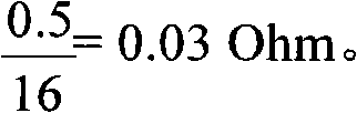
The effective output impedance of the drive circuit 20 of third level 11-3 is summations of output impedance of each drive circuit 20 of charger 10.Yet, it will be appreciated that, be configured to have low output impedance by drive circuit 20 with each grade, the virtual value in the output impedance can be remained on the Low ESR grade.As seen, when every grade output impedance is 0.03Ohm, (for example, as 16 examples that transistor is right given herein) effective output impedance of afterbody drive circuit will be lower than 0.1Ohm, still provide good voltage transitions to load, even have under the low-impedance situation (for example, even when load has voltage ratio between impedance, load and the source end of 1.0Ohm and is higher than 90% (90.9%)) at transducer.
In another aspect, the charger 10 that comprises placed in-line a plurality of grades of 11-1,11-2,11-3 can comprise a main timing control unit 35.Main timing control unit 35 can be independent of each level.Main timing control unit 35 can move to control the frequency of each power stage 11-1,11-2,11-3 switching.Main timing control unit 35 can move so that switching each level on certain frequency or on different frequencies.Mentioned and similarly to be configured each grade 11-1,11-2,11-3.For example, each grade 11-1,11-2, the 11-3 transistor that can have the parallel connection of similar number to arrange is right.In other examples, each grade 11-1,11-2,11-3 can have the transistor of different numbers right, and every grade has the transistor of scope from 1 to N to number.
The feature of the charger drive circuit that provides of Fig. 2 to 4 is the output signal and the high electric current fan-out capability of low output impedance, low voltage generally.Having illustrated can be by providing as shown in Figs. 3-4 a plurality of parallel transistors to reducing the output impedance of drive circuit 20.Equally, can be by providing the parallel transistor shown in Fig. 2 circuit to increasing the electric current fan-out capability of drive circuit 20.The electric current fan-out capability of drive circuit 20 is approximately the summation of the right output mos FET electric current fan-out capability of each independent transistor.For example, in the drive circuit of Fig. 2, have the right single transistor of a transistor that is formed on the integrated circuit 302 drive circuit is had about 10 amperes electric current fan-out capability.Having in these right embodiments of eight (8) the individual transistors of arranging in parallel of Fig. 2 to 3, when these transistors when being formed on the less MOSFET integrated circuit of structure, the electric current fan-out capability is approximately 80 amperes.By increasing or reduce the right number of arranging of transistor in parallel in the drive circuit 20, can improve or reduce the electric current fan-out capability of drive circuit 20.Similarly, the output impedance of drive circuit 20 is along with extra transistor is reduced adding drive circuit 20.In the embodiment of Fig. 2, drive circuit 20 shows a single-transistor to drive circuit, and drive circuit 20 has the output impedance of 0.5Ohm.In the embodiment of Fig. 2 to Fig. 3, wherein drive circuit 20 have eight (8) the individual transistors of arranging in parallel to and these integrated circuits given herein, the output impedance of drive circuit 20 is approximately
By increasing or reduce the right number of arranging of transistor in parallel in the drive circuit 20, the output impedance of drive circuit 20 can be adjusted to desirable output impedance.
According to the peak power theory, when the output impedance of the impedance of load and power supply was complementary, peak power just was sent in the load.In some embodiments, device 1000 can be configured to make that the impedance of load and the impedance phase of drive circuit 20 mate.Yet in other embodiments, load impedance is unmatched with respect to the impedance of drive circuit 20, drive circuit can be provided as (for example has low output impedance, less than 0.5Ohm), and install 1000 and can be provided as and make the ratio of the output impedance of drive circuit 20 and load impedance less than 1/10.Output impedance is provided as low value (for example, less than 0.5Ohm) and further makes the ratio of output impedance and load impedance provide several advantages less than 1/10.For example, drive circuit 20 is configured to have low output impedance and Low ESR ratio (for example, 1/10 or littler impedance ratio) and has produced high energy conversion efficiency.Most of substantial energy all is sent in the load (that is, transducer 90).Like this, when drive circuit 20 heating, the energy of loss is considerably less.Such result is particularly advantageous, and for example the heat that produces at device 1000 may constitute in the medical applications of harm patient.For being provided in the application of power supply 50 by one or more batteries arbitrarily, high-energy conversion efficiency embodiment given herein has produced significant advantage at battery aspect service life.Keep low drive circuit output impedance and impedance ratio also to guarantee source voltage very closely corresponding to load voltage, that has therefore improved device can handling and ease for use.The voltage that is sent on the transducer 90 can be set by setting up source voltage basically.
When drive circuit 20 is in running order and when drive circuit 20 outputs had the driving signal of a frequency (for example reaching the resonant frequency of transducer 90), drive circuit 20 given herein can comprise a source voltage that is associated.Drive circuit source voltage can directly record by the voltage on the lead-out terminal of measuring drive circuit in the open-circuit condition (do not having under the situation of electric current, do not having voltage on the impedance of the drive circuit contribution parts).In addition, when a load is attached between the lead-out terminal of drive circuit, and when drive circuit drives this load (for example with the corresponding frequency of resonant frequency on), the voltage in the load can be expressed as
V
Load=
V Source R Load
R
Source+ R
LoadEquation 1
R wherein
SourceOutput impedance for drive circuit 20.Therefore, the voltage in the load (transducer) and the ratio of source voltage can be expressed as
V
Load/V
Source=
R Load
R
Load+ R
SourceEquation 2
Therefore, when the output impedance of drive circuit 30 went to zero, load voltage more closely was similar to source voltage as can be seen.In addition, be configured so that by installing 1000 the ratio of source output impedance and load impedance remains on 1/9 or lower as can be seen, the amplitude of the voltage of leap load will remain on 90% or higher with respect to the amplitude of source voltage on the drive circuit.Provided the different embodiments of device 1000 at this with this ratio.In other embodiments given herein, the ratio of load voltage and source voltage is 95% or higher, and is 99% or higher in other embodiments.Below in Table A, provided expection example with desired related data.
Table A
Drive circuit 20 is configured to comprise that another advantage of low output impedance and Low ESR ratio is that this configuration has reduced the side-play amount in the resonant frequency of transducer 90.Referring to Fig. 7, show the resonant frequency (by a frequency that drives signal of drive circuit 20 outputs, ultrasonic transducer 90 Maximum Power Outputs on this frequency) of transducer 90 and the curve chart of the source output impedance of drive circuit 20.When source output impedance increased, resonant frequency was offset (in described example from about 1.51MHz to about 1.63MHz) significantly.Can handling and ease for use by what reduce that source output impedance reduces that the resonance frequency shift amount can improve device 1000, its reason is to approach more for a viewed resonant frequency of concrete transducer the nominal resonant frequency (generally provided by the manufacturer of this transducer and determine according to the material behavior of transducer 90) of this concrete transducer.
Other advantages referring to the low output impedance High Output Current of configuration driven circuit 20, high electric current fan-out capability on the drive circuit 20 (be approximately in some embodiments 50 amperes or higher (and the embodiment of low current fan-out capability is advantage in some applications)) electric current fan-out capability allows to use high-energy output on transducer 90 of low pressure (and in a plurality of embodiments, approximately being 50V or lower or 25V or lower) less than 100V (about in some embodiments 50 watts or higher).This functional the high energy of low pressure (only have output) is favourable in a lot of the application, is included in the multiple medical applications, wherein owing to for example be exposed to 100V or higher high pressure has constituted risk to patient or care-giver near transducer 90 down.Yet in some applications, the output that surpasses 100V is favourable.
In one embodiment, the device that to produce hyperacoustic device 1000 can be a kind of single-mode, this device have fixed (not interchangeable) transducer 90 and start this device at every turn and have of same feature and drive signal to export its output when driving signal.In another embodiment, producing hyperacoustic device 1000 can be a kind of multi-mode device, and this device can be exported the driving signal with different characteristic constantly in difference.Device 1000 can move and make device 1000 output has one of one group of different characteristic and drives signal in response to the operator in the user interface that is input to device 1000 imports control.When device 1000 is provided as when making that its transducer assemblies is one of a plurality of interchangeable candidate's transducer assemblies, be attached to transducer assemblies on the charger 10 in response to current in these candidate's transducer assemblies, device 1000 can move and make different output drive signals with one group of different characteristic of its output.
Distribution in the embodiment of Fig. 4 and control circuit 40 comprise a three-way switch integrated circuit 404.The operator manually moving switch integrated circuit 404 in case between OFF position and ON position change-over switch integrated circuit 404.In the ON position, the electric energy of power supply 50 is connected on the clamp voltage terminal of drive circuit 20.The charger earth terminal can be used for isolation+5V and+the 12V power supply, thereby reduce the wiring burden.In another aspect, distribution and control circuit 40 can comprise a control unit 410.Control unit 410 can be by having a microcontroller or microprocessor to provide.Control unit 410 can be associated with memorizer 412, and memorizer 412 can be stored different data, routine data, and can set up data to determine the feature by the output signal of drive circuit 20 outputs.Control unit 414 can communicate with display 414, and this display can be configured to have user interface capabilities.
For the additional features of controlling feature that comprises of exhibiting device 1000, Fig. 4 shows the more detailed sketch map of the charger shown in the block diagram of Fig. 3.In Fig. 4, show drive circuit 20, timing circuit 30, distribution and control circuit 40 and power supply 50.In one embodiment, power supply 50 can comprise the chargeable set of cells of NI-G of a plurality of 9.6V, 1600mAh.In another embodiment, power supply 50 can comprise an AC to the DC transducer to be connected on the AC wall outlet.These set of cells can be for example from the set of cells of the obtainable numbering 23-432 of RadioShack company.Charger 10 can also comprise rotary switch 402 and the three-way switch 404 that forms distribution and control circuit 40.The user can transmit to the power of transducer with the increment of the 9.6V scope adjusted at ± 28.8V by MOSFET.Can comprise extra battery so that increase the power source voltage scope.Blueness in Fig. 4 embodiment " is opened " LED306 and is connected in the off/on switches, off/on switches by having bypass capacitor equally 5V and the pressure regulator of 12V 1A provide electric energy to crystal oscillator integrated circuit 304 and pin driver IC 302.In positive Neil-Kang Saiman bayonet socket (BNC) adapter on the output termination pro-panel of device.The battery recharger port (not shown) that is positioned at the back of system connects with lead and is used for six series batteries are charged.For system is charged, device is switched to the closed position and rotary switch is moved on the disconnected terminal that device panel subscript shows.
A user interface that produces hyperacoustic device 1000 can partly be provided by switch 402 and switch 404, switch 402 and switch 404 can be used with the voltage on the control clamp voltage terminal 220,222 by the operator, and user interface can partly be provided by switch 406.A user interface that produces hyperacoustic device 1000 can also comprise extra control actuator.For example, device 1000 can be configured so that display 414 shows the different virtual control knob that is activated by the operator.Figure 7 illustrates an example of device 1000, display 414 is configured to comprise an interface control knob in this example.
In the example of Fig. 7, device 1000 can move and make button 430,432 can be used for regulating the voltage on the first clamp voltage terminal 220, button 438,440 can be used to control the voltage on the second clamp voltage terminal 222, button 444,446 can be used to control the driving signal frequency by drive circuit 20 outputs, and button 450,452 can be used to control the pattern of low output drive signal, so that for example select between " continuous mode " or " pulse mode ".In the embodiment given herein, control unit 410 can with switch 402 and 404 communicate such service voltage switch 402,404 or button 430,432,438,440 can regulate voltage on the clamp voltage terminal 220,222.In preview area 460, when using one group of current control parameter, can show a kind of displaying of the output drive signal of expection output at this.In order to use user interface control output drive signal frequency, control unit 410 can be connected on the timing means 304 communicativeness, shown in the sketch map of Fig. 4.Timing means (as the crystal oscillator integrated circuit that provides specially) can be chosen as programmable, like this can be by be chosen in a frequency in certain frequency range to control of device input.In order to enlarge selectable frequency range, can in timing circuit 30, comprise a plurality of timing means with eclipsed frequency range.Can provide suitable multi-channel conversion circuit (not shown) to be used to allow select the timing means that is fit to based on institute's selected frequency.
(wherein transducer 90 is transducers of one of interchangeable transducer of a plurality of candidates in some embodiments of installing 1000, the interchangeable transducer of these candidates is combined in one of transducer assemblies of a plurality of correspondences) in, a device output drive signal of 1000 can in response to current be attached on the charger 10 transducer assemblies (for example, referring to Fig. 1, transducer assemblies A or transducer assemblies B).In described specific embodiments, interchangeable transducer assemblies A and B combine transmission line 70 and probe 80.Yet in another embodiment, the plug-in package that combines the device 1000 of a transducer (being transducer assemblies) can only comprise probe 80, and wherein transmission line 70 is fixed parts.In another embodiment, a transducer assemblies that combines transducer 90 can in fact only comprise transducer 90.In fact only the transducer assemblies that is made of transducer 90 may be provided in a plug in the parts of circuit board.Can adjust the feature this point of an output drive signal in response to a transducer assemblies in the current a plurality of transducer assemblies that are attached on the charger 10 for device 1000, each candidate's transducer assemblies can have the associative storage 900 (referring to Fig. 1) of an identifier that storage is used for transducer, and for example its form is a text based alphanumeric number.As shown in Figure 1, memorizer 900 can be accommodated in the housing 82 of probe 80.
Device 1000 can move and make when new transducer assemblies (for example, A, B and another assembly, C or the like) when being attached on the charger 10, the transducer assemblies identifier information that is stored in the memorizer 900 is delivered on the control unit 410 by the communicator 902 that is fit to.For example, control unit 40 and memorizer 900 can be by by the two-wire interface (I of Philip for example
2The C bus) communicator 902 that provides communicates.Control unit 410 can move and make control unit 410 in response to the recognition data that between memorizer 900 and control unit 410, transmits set up suitable being provided with export have one group of concrete feature the driving signal to drive the current ultrasonic transducer that is attached to the concrete transducer assemblies on the charger 10.
The output drive signal feature that can produce output drive signal in response to the transducer assemblies that is associated by the data of transmission expression transducer assemblies identity below has been described.In another embodiment, device 1000 can move and make output drive signal characteristic response by drive circuit 20 outputs in the transducer that is associated, and its mode is controlled for being attached to one group of specific timing circuit on the transducer assemblies in candidate's transducer assemblies by use.
In an example, as explaining referring to Fig. 1, each transducer assemblies in one group of candidate's transducer assemblies (they can be or can not be a whole set of candidate's transducer assemblies) can be equipped with a timing means that is associated.As shown in Figure 1, crystal oscillator integrated circuit 304 can be attached on the transducer assemblies A, and crystal oscillator integrated circuit 304 can be attached on the transducer assemblies B.Each crystal oscillator integrated circuit 304 can have associating communication devices 305 so that communicate with the remaining part of timing circuit 30.Communicator 305 can comprise a copper cash.Device 1000 can move and make the timing means that will be attached to when new transducer assemblies is attached on the charger 10 on this new transducer assemblies activate so that one or more output characteristics of control output drive signal.Referring to the example of Fig. 1, device 1000 can move and make that when transducer assemblies A was attached on the charger 10, the timing of 304 pairs of output drive signals of timing means of transducer assemblies A was controlled.Device 1000 can also move and make when transducer assemblies B is attached on the charger 10, controls with 304 pairs of timings by the output drive signal of drive circuit 20 outputs of the timing means that has transducer assemblies B to place.
Now will be referring to the ultrasonic transducer 90 of probe 80.Probe 80 ultrasonic transducer 90 can be by (EBL Products, Inc.) obtainable radius of curvature provides for PZT-4, a 1.54MHz of 1.5 type and the piezoelectric ceramics of diameter 0.75in from EBL Products Co., Ltd.This transducer of EBL Products Co., Ltd by manufacturer given the nominal resonant frequency of 1.5MHz.Housing 82 can be provided by polrvinyl chloride (PVC) effect plastic assembly.This assembly can use that (Sherline Products, Inc.) obtainable miniature lathe and milling system customize from Sherline Products Co., Ltd.The transparent propene of housing 82 fronts is as the protectiveness of ceramic transducer 90 surface and as bearing in focus in the face of the ultrasonic energy of transducer 90 emissions.With regard to the element that this place is mentioned, this mention element " 90 " will be considered to mention this place referring to concrete transducer in any one, for example transducer 90,90A, 90,90B or the like.
Transducer 90 can use the transmission line 70 that is provided by 22 wire gauge coaxial cables to connect, and 22 wire gauge coaxial cables end at adapter 72 (Figure 21), and adapter 72 can be provided by cloudy bnc connector.Transducer 90 can have power output characteristic shown in Fig. 8,9,10 and 11 and impedance characteristic shown in Figure 12.The peak power curve of output has been shown in Fig. 8, Fig. 9, Figure 10 and Figure 11, these curves are to use Mason's Model Calculation to draw at the different transducers that the drive circuit by the difference configuration drives, and the drive circuit of these different configurations has different output impedance on frequency range.The power output curve diagram of Fig. 8 at be transducer with 1.5MHz nominal resonant frequency and 10.3Ohm impedance.The power output curve diagram of Fig. 9 at be transducer with 1.5MHz nominal resonant frequency and 1.2Ohm impedance.The power output curve diagram of Figure 10 at be transducer with 8MHz nominal resonant frequency and 10.6Ohm impedance.The power output curve diagram of Figure 11 at be transducer with 8MHz nominal resonant frequency and 0.37Ohm impedance.The resonant frequency of ultrasonic transducer 90 can be considered to the residing frequency of peak power that ultrasonic transducer sends when the driving (that is to say and drive this transducer) that is subjected to by the output drive signal of drive circuit 20 output.Referring to Fig. 6, and refer again to the power output curve diagram of Fig. 8, Fig. 9, Figure 10 and Figure 11, can see that resonant frequency will the skew a little along with the increase of the output impedance of drive circuit 20.With regard to " resonant frequency " referred in this, be to be understood that several factors can influence the resonant frequency of transducer, for example, the impedance of the output impedance of drive circuit 20, transmission line 70.However, when the primary determiner that the frequency of resonance takes place when transducer 90 is the material properties of transducer, mention that " resonant frequency of transducer " is exactly suitable.Equally, if the output impedance of drive circuit 20 and transmission line 70 roughly remain on low-level on, the influence of drive circuit output impedance and transmission line impedance can be ignored.
In Figure 12, the impedance that shows mentioned PZT-4,1.5MHz (nominal resonant frequency), 8Ohm transducer can use the known metering method of standard that for example is used to measure impedance to measure to the impedance characteristic of the curve chart ceramic transducer of frequency.In the example of illustrated transducer 90, the impedance of transducer 90 is that it is minimum on the impedance measuring equipment frequency of about 1.5MHz, is approximately 8.0Ohm.Referring to Figure 12, the impedance measuring equipment frequency that the impedance of transducer 90 is in its minimum can be considered to the measurement to the resonant frequency of transducer 90.Yet as noted, when being activated circuit 20 drivings, the resonant frequency of transducer 90 is estimated partly to depend on the feature of drive circuit 20.According to definition, when being activated on resonant frequency, the output of the power of transducer 90 is in its top level.Resonant frequency can be expressed as a point value, and (for example, 1.54MHz) or be expressed as a frequency range, power output is higher than a predetermined percentage rate (for example, 90%) of peak power output valve on this frequency range.Can be considered to be in a resonant frequency frequency on every side of representing at a point value place with the corresponding driving frequency of resonant frequency.Can also be considered to a frequency within the resonant frequency range with the corresponding driving frequency of resonant frequency, resonant frequency is expressed as a frequency range here.
Point out that charger 10 can move and make an output drive signal that drives transducer 90 can have and the corresponding frequency of the resonant frequency of transducer 90.In another aspect, an output drive signal by charger 10 outputs that charger 10 can be configured so that to be used to drive transducer 90 can vibrate between generating positive and negative voltage.
Being equipped with charger 10 comes output drive signal to be used for driving to comprise that the polar transducer 90 of positive and negative provides a plurality of significant advantages.Referring to transducer 90, it can shrink usually when one first polar voltages is applied on the transducer 90, and it will expand when one second polar voltages is applied on it.Therefore, apply and have polar one of positive and negative and drive signal the pressure variation is provided, this pressure is applied on the transducer 90 causing hyperacoustic emission, thereby has increased the life-span of transducer 90.In another aspect, provide the driving signal of positive-negative polarity to cause any voltage of staying of transducer 90, thereby offset the amplitude that has also therefore reduced in voltage with vibration.Still, further use the bipolarity output drive signal to allow to use transistor to (for example, transistor 204 shown in Figure 2, transistor 206) positive and negative two passages, this has just reduced the right heat exhaustion of transistor and has increased the right electric current fan-out capability of transistor, thereby allow higher power output, voltage is reduced to below the danger level.(it will be appreciated that, be applied in the load ± signal of 50V produces and ± identical the output of 0V to 100V driving signal, but has quite safe electric pressure).
In another aspect, charger 10 can move and be used to export a unbalanced bipolar signal to drive transducer 90.In one embodiment, " unbalanced " bipolar signal herein can have 1V or bigger difference in magnitude (for example ,+10V to the-unbalanced bipolar signal of 9V) between first and second utmost points; In another embodiment, 5V or bigger difference in magnitude (for example ,+5V to the-unbalanced bipolar signal of 10V); In another embodiment, 20V or bigger difference in magnitude (for example ,+100V to the-unbalanced bipolar signal of 80V); And 40V or bigger difference in magnitude (for example ,+30V to the-unbalanced bipolar signal of 70V) in another embodiment.In the exploitation of device 1000, determined that it is to have increased that transducer 90 bears the ability that is applied to the compression stress on it for expansionary force.It can shrink when a negative voltage driving signal is applied on the transducer 90, it can expand (perhaps alternately when signal was applied on it and when a positive voltage drives, depend on setting, shrink when positive voltage drives signal, and expand when applying a negative voltage driving signal) when applying.However, drive signal with generating positive and negative voltage and drive the variation that transducer 90 has advantageously produced the moving range of transducer 90.By providing charger 10 outputs a uneven bipolar drive signals, compression stress and expansive force all are applied on the transducer 90, and the compression stress that is applied on the transducer 90 can be bigger than the expansion intensity of force.
Refer again to Fig. 4, to install 1000 provide and make the operator of the user interface input by operative installations 1000 import control can adjust independently positive clamper terminal voltage and negative clamper terminal voltage the two, this allow by the output drive signal of drive circuit 20 outputs by accurately be tuned to the limit determined by the physical characteristic of transducer 90, and can not exceed this level.
Referring to table B, in conjunction with exemplary drive signal the difference expection example of transducer assemblies to be summed up, these exemplary drive signal are associated with each transducer assemblies.
Table B
The feature of the output drive signal that is fit to that is associated with transducer assemblies A, B, C, D, E and F is summarised among Figure 13, Figure 14, Figure 15, Figure 16, Figure 17 and Figure 18.In the table B that is showed and Figure 13 to Figure 18 of being associated, output drive signal is shown as and the resonant frequency of transducer 90 identical (to the two-decimal point).Should be appreciated that owing to tolerance, actual driving signal can be corresponding to a resonant frequency incomplete same with this resonant frequency.
Referring to Figure 13, shown unbalanced bipolarity output drive signal has+the possible positive voltage peak of 30V and-negative voltage peak of 70V.The operation of the output drive signal of Figure 13 is used to produce the compression stress that is applied on the transducer 90, and the amplitude of this compression stress is greater than expansionary force.Device 1000 can be provided as and make the feature of driving signal of Figure 13 to control to be provided with, perhaps to be provided with in response to the concrete transducer assemblies that is attached on the charger 10 in response to the operator of the user interface of operative installations 1000 input.Operation at device 1000 in response to concrete transducer assemblies (for example is used for, A, B, C, D, E, F) the attached situation of exporting a driving signal with concrete feature under, device 1000 also further can move and make the feature that drives signal can pass through further experience change of control input, and these control inputs are imported by the user interface of operator's operative installations 1000 after attached finishing.
Figure 13, Figure 14, Figure 15, Figure 16, Figure 17 and Figure 18 have showed a plurality of driving signals, and these drive signal and can be provided with and/or be provided with in response to the concrete transducer assemblies that is attached on the charger 10 in response to the control input of being imported by the user interface of operator's operative installations 1000.Above in this characteristic presentization with the driving signal of Figure 13.Referring to the output drive signal of Figure 14, the output drive signal of Figure 14 is an equilibrated bipolarity output drive signal that is suitable for driving transducer assemblies B, and transducer assemblies B has transducer 90,90b.Referring to the output drive signal of Figure 15, the output drive signal of Figure 15 is the sinusoidal output drive signal of a unipolarity that is suitable for driving transducer assemblies C, and transducer assemblies C has transducer 90,90c.Referring to Figure 16, the output drive signal of Figure 16 is a unbalanced double polarity sine driving signal that is suitable for driving transducer assemblies D, and transducer assemblies D has transducer 90,90d.Referring to the output drive signal of Figure 13 to 16, the output drive signal of Figure 13 to 16 can be considered to " successive " and drive signal, because they do not have multiple null cycle between cycle of oscillation.The driving signal of Figure 17 can be considered to a pulse signal, because it is free period p at the mid portion of cycle of oscillation
nIn some applications, for example imaging, device 1000 can move mid portion output p null cycle that is used in cycle of oscillation
nTo preserve energy, p null cycle here
nCan not influence the function of device 1000 negatively.In some imaging devices, for example, only need come carrying out timing cycle of oscillation with exposure cycle.
Visual means 1000 can be configured to cause the switching between the operational mode of the switching generator 1000 between the transducer assemblies of device 1000.For example, under the situation of transducer assemblies A, device 1000 can be operated in the pattern attached, wherein installs the unbalanced bipolar drive signals of 1000 outputs.Device 1000 can also be configured to make that the operational mode of device 1000 changes in response to the current attached transducer assemblies that is switched, for example change (when transducer assemblies B is attached), perhaps drive the operational mode of signal and change (when transducer assemblies C is attached) in response to unipolarity of output in response to bipolarity balance of output drives the operational mode of signal.
In one embodiment, as shown in figure 19, transducer 90 can be provided by a single element of transducer, for example has a single transducer disc 91 of certain impedance and nominal resonant frequency.In one embodiment, as shown in figure 20, transducer 90 can comprise a plurality of many element of transducers, for example a plurality of transducer discs of series connection arrangement.In a specific embodiments, when the drive circuit 20 that is subjected to certain configuration drove, a plurality of element of transducers (for example, ceramic disk) can have specific related rated power and specific resonant frequency separately.In the example of Figure 20, transducer 90 comprises three (3) individual element of transducers 91.Yet transducer 90 can also comprise for example two (2) individual element of transducers or N element of transducer.
Referring to table B, element of transducer F has showed following operating position, and wherein transducer assemblies comprises a transducer with a plurality of transducer discs, and each transducer disc has different nominal resonant frequency and resonant frequency.These elements all comprise a transducer disc from EBL Products Co., Ltd obtainable PZT series element of transducer separately.This transducer can advantageously use a driving signal shown in Figure 180 to drive.The driving signal of Figure 18 is that a frequency sweep with change frequency drives signal.In period p
1Process in, drive signal and have the frequency of 1.52MHz, this frequency is corresponding with the resonant frequency of first element of transducer.In period p
2Process in, drive signal and have the frequency of 4.15MHz, this frequency is corresponding with the resonant frequency of second element of transducer.In period p
3Process in, drive signal and have the frequency of 6.51MHz, this frequency is corresponding with the resonant frequency of the 3rd element of transducer of transducer 90F.
Figure 21 illustrates the entity form view of ultrasonic generator 1000.Charger 10 can be small-sized with light-duty, for example about 5 pounds.The housing 12 of charger 10 can have about 4 * 6 * 2 inches
3Size.The housing 82 of probe 80 can be provided by polrvinyl chloride (PVC) effect plastic assembly.Referring to housing 82, ultrasonic transducer 90 (shown in broken lines) can be accommodated in the far-end of housing 82 as shown in figure 21, and support part 84 can be arranged to from the far-end of housing 82 and extends.Support part 84 can limit a cavity 86.Cavity 86 can be adapted for and receive a kind of coupling connection medium.For example the such coupling connection medium of ultrasonic fluid or water can be positioned in the cavity 86.The ultrasonic fluid coupling connection medium that is fit to is the ultrasonic fluid of the obtainable numbering NTNMAA001X of medical association (NMA) from the world.In some applications, device 1000 probe 80 can be adapted for and make and replacedly to remove support part 84 from housing 82.In addition, support part 84 can be provided as comprise parts 84 for example ' and 84 " one of one group of candidate's support part.Support part 84 can comprise a transmissive wall 85.Best as seen as the view of Figure 23, transmissive wall 85 can be printing opacity to allow visually to observe the inside of cavity 86.Shown in the front view of Figure 22, make the transducer periphery 91 shown in the with dashed lines, the periphery of support part 84 can roughly align with the periphery of support part 84 on the interface between transducer 90 and the support part 84.As best visible in Figure 23, transmissive wall 85 allows operators to observe the inside of cavity 86, for example to determine the coupling connection media processes quality (for example, whether coupling connection medium is foamless basically) at cavity inside.Transmissive wall 85 can partly center on the periphery of support part 84 and form.In the embodiment of Figure 23, transmissive wall 85 is formed the periphery that centers on support part 84 fully.Transmission line 70 can have the length of about 1m.In another embodiment, can cancel transmission line 70 and charger 10 and transducer 90 can being installed in the common housing.
Additional housing and the package feature of the device 1000 in the embodiment have been provided referring to Figure 24 and 25.Figure 24 and 25 shows the vertical view and the bottom view of the printed circuit board (PCB) 15 of the MOSFET integrated circuit 202 that carries drive circuit 20.In the view of Figure 24 and 25, the position of dashed boundaries 12 expressions housing 12 when printed circuit board (PCB) 15 is placed in the housing 12.In the embodiment of Figure 24, MOSFET integrated circuit 202 can be distributed on the outer peripheral edges of circuit board 15, and integrated circuit 202 is compared the periphery that approaches printed circuit board (PCB) 15 more with the imaginary centres axis 17 of the longitudinal extension of printed circuit board (PCB) 15 like this.In the embodiment of Figure 24 and 25, each MOSFET integrated circuit 202 of drive circuit 20 comes to this localized.Close housing border 12 as described distributes and just more likely the heat of integrated circuit 202 generations is transmitted to the outside of housing 12, thereby will remove and increase the power output capacity of MOSFET integrated circuit 202 and drive circuit 20 from integrated circuit 202 heats.
Referring to the circuit diagram of Figure 24 and 25, the output of drive circuit 20 can be included in a plurality of MOSFET integrated circuits of a common node 250 place's co the output of each.As seen entity by Figure 24 and 25 constitutes view, and common node 250 can be made up of the output voltage plane of planar configuration on entity.Being configured to a planar common node 250 of output voltage can be distributed on the 2 dimensional region of printed circuit board (PCB) 15 so that partly limit one or more surfaces of printed circuit board (PCB) 15.In the embodiment of Figure 24 and Figure 25, the output voltage plane is distributed as one of the top surface that partly limits printed circuit board (PCB) 15 and basal surface.Go out as shown, the common node 250 that is provided by the output voltage plane can comprise and is exposed to an outside plane surface or printed circuit board (PCB) 15.The common node 250 that is provided by an output voltage plane shown in Figure 24 and 25 can form from the copper surface of printed circuit board laminated material, and this laminated material passes through suitable etching and is provided as the right correspondence output of different crystal pipe of common connection drive circuit 20.Because common node 250 is made of the planar conductor on the surface that limits printed circuit board (PCB) 15, removed significant heat from installing 1000 circuit block (comprising MOSFET integrated circuit 202), therefore increased the power output capacity of MOSFET integrated circuit 20 from drive circuit 20.The common node 250 that is provided by the output voltage plane can be distributed as and make the electric insulation part branch of output voltage plane and a plurality of (and being each in one embodiment) MOSFET integrated circuit 202 be in thermo-contact or be similar to thermo-contact.Use this configuration, encouraged the distribution of heat energy to the end at this, make so each of a plurality of MOSFET integrated circuits 202 and in one embodiment each MOSFET integrated circuit have roughly the same operating temperature.Drive circuit 20 is configured so that each MOSFET integrated circuit 200 has roughly the same operating temperature and reduced the noise of being exported by drive circuit 20.Say definitely, drive circuit 20 is configured so that each MOSFET integrated circuit 200 has roughly the same operating temperature and can expect that minimizing may produce the vibration of ripple and noise and the difference on the switch fixed cycle operator in the output of drive circuit 20.
In one embodiment, system is accommodated in by 4 * 6 * 2 inches
3The housing 12 (such housing is provided by Serpac company, numbering 073) that provides of waterproof plastic encapsulation in.This housing passes through two single pull-alongs rotary switches with (1.5 * 2 * 1 inch in circuit
3) and six 9.6V, 1600mAh Ni-Cd nickel-cadmium groups (can obtain to number 23-432) from RadioShack company be cascaded.
Refer again to Fig. 1, can adopt specific mode to coordinate the different impedances of drive circuit 20, transmission line 70 and transducer 90.In one embodiment, drive circuit 20 has the output impedance that is approximately 0.5Ohm.Drive circuit 20 is provided as has output impedance that the impedance with transducer 90 is not complementary and improved and install 1000 thermal conversion efficiency.Have low output impedance by drive circuit 20 is provided as, only have energy seldom in drive circuit 20, to dissipate as heat.Therefore, drive circuit 20 will remain in a kind of state, and this state is safe for touch in the entire work process of drive circuit 20.
The impedance of transmission line 70 can also be coordinated with the output impedance of drive circuit 20 and the impedance phase of transducer 90.In an example, transmission line 70 can be provided as the resistance value with the output impedance that is approximately drive circuit 20, the output impedance of the impedance of transmission line 70 and drive circuit 10 is complementary like this, but is similar to drive circuit 20, and transmission line 70 is unmatched for transducer 90.
In the process of development device 1000, determined by impedance configuration to be that low value (for example about 5Ohm or lower, and in other embodiments, be 1Ohm or lower) has embodied a plurality of advantages with transmission line 70.In an example, the transmission line 70 that is provided by coaxial cable is provided by the obtainable 5Ohm coaxial cable of Cooner Wire company (part number 1/22-15044) of looking into special Ellsworth city from the California.By many coaxial cables in parallel are provided, can reduce the impedance of transmission line 70.When providing many coaxial cables with the form of parallel connection in the formation of transmission line 70, the impedance of transmission line 70 can be expressed as
R wherein
CBe the impedance of each independent cable, and N is the number of cable.Therefore, comprise that at transmission line 70 transmission line impedance will be less than 1Ohm in the situation of six (6) individual mentioned coaxial cables.Can in a kind of specific structure, arrange many cables.In the embodiment of Figure 25, transmission line 70 is to be provided by many braided coaxial cables of arranging in parallel.In the embodiment of Figure 26, transmission line 70 is to be provided by many twisting formula coaxial cables of arranging in parallel.Ad hoc structure shown in Figure 25 and 26 is used to reduce noise.
[select from U.S. Provisional Application number 61/079,712 with the lower part, only do a small amount of form and the modification of editor's property.]
We have developed a kind of portable high-power ultrasonic system with low output impedance amplifier circuit (being lower than 0.2Ohm) very, and this system can will be converted to ultrasonic transducer from 95% to 100% of the energy of battery supply.Since impedance do not match make in reflection/heating loss energy seldom and battery big electric current can be provided, therefore need just can produce therapeutic acoustic energy ripple by lower voltage.Described system can go up from PZT-4 at therapeutic domain (being higher than 50 watts), and the piezoelectric ceramics of 1.54MHz, 0.75 inch diameter produces acoustic energy output.It is a light-type (being lower than 6 pounds) portable (2x6x4 inch), and is powered by rechargeable battery.Portable therapeutic ultrasound device might replace the radio frequency amplifier that uses in " plug-in " medical system and the research.The on-the-spot use of its internal cell can be leaned on by this system, makes it be particularly suitable for military affairs, first aid and long-range/on-the-spot or medical applications of making a round of visits.
Over the last couple of decades, medical ultrasound as a kind of releasing arthritis, improve rehabilitation and strengthen the instrument that wound healing handles and caused that the attention of medical profession is (referring to " the emerging therapeutic ultrasound " of J.Wu and W.L.M.Nyborg, medical supersonic, ISBN 978-981-256-685-0 (printing edition), 2006; " the present situation-review in carcinoma of prostate of HIFU and cryotherapy "-European urology of G.Aus, volume 50, the 927-934 pages or leaves, 2006; " treatment sound: ultrasonic use in administration and other treatment application "-comment naturally of S.Mitragotri: drug discovery, volume 4, the 255-260 pages or leaves, 2005; And M.R.Bailey, V.A.Khokhlova, O.A.Sapozhnikov, " physical mechanism of ultrasonic therapeutic effect: (review) " of S.G.Kargl and L.A.Crum, acoustics physics, 49, the 4 phases of volume, 369-388 page or leaf, 2003).More the ultrasonic of high energy plays a role in surgery is used, for example the prostate treatment and the cerebral tumor and heart tissue are peeled off, (referring to M.R.Bailey, V.A.Khokhlova, O.A.Sapozhnikov, S.G.Kargl, and L.A.Crum " physical mechanism of ultrasonic therapeutic effect: (review) ", the acoustics physics, volume 49, the 4th phase, 369-388 page or leaf, 2003; " high intensity focused ultrasound: physical principle and device " of G.ter Harr and C.Coussios, international thermotherapy journal, volume 23, the 89-104 pages or leaves, 2007; N.I.Vykhodtseva, K.Hynynen, " the high intensity pulses ultrasonic irradiation of subharmonic emission is to the tissue influence of live body Medulla Leporis seu Oryctolagi " of C.Damianou, ultrasound medicine and biology, volume 21, the 969-979 pages or leaves, 1995; D.Cesario and et al. " Selection of Ablation Catheters; Energy Sources; and Power Delivery " Contemporary Cardiology, Atrial Fibrillation, pp.209-221, ISBN:978-1-58829-856-0 (Print) 978-1-59745-163-5 (Online), 2008.
<0{ 〉People's such as D.Cesario " selection of ablation catheter, the energy and power output ", contemporary cardiology, auricular fibrillation, 209-221 page or leaf, ISBN:978-1-58829-856-0 (printing edition) 978-1-59745-163-5 (online version), 2008.Therapeutic ultrasound and the effect in tissue signature thereof are at present just under study for action.For example, research worker are being assessed ultrasound wave and are being changed the ability of macromole percutaneous dosing in the application (referring to E.J.Park in the directed chemotherapy administration of the brain cancer and at cytogene, K.I.Jung, and S.W.Yoon " being used as the acoustics mechanism of the booster of percutaneous dosing ", Acoustical Society of America's periodical, roll up 107, the 2788 pages, 2005; G.K.Lewis, Jr., W.Olbricht, and G.K.Lewis " acoustics in the nervous tissue strengthens the blue dye perfusion of ivens ", Acoustical Society of America, POMA, volume 2,2008; " gene therapy progress and the prospect: be used for the ultrasonic of gene transfer " of C.M.H.Newman and T.Bettinger, gene therapy, volume 14, the 465-475 pages or leaves, 2007).The current potentiality of a kind of compound portable ultrasound imaging and therapy system of studying with might and main are to be used for military affairs and medical application (referring to F.L.Lizzi, D.J.Driller, R.H.Silverman, B.Lucas, and " therapeutic ultrasound "-S.Vaezy of A.Rosado, X, Shi, R.W.Martin, E.Chi, P.I.Nelson, M.R.Bailey, and L.A.Crum " using the real-time visual of the high intensity focused ultrasound processing of ultra sonic imaging ", ultrasound medicine and biology, volume 27, the 32-42 pages or leaves, 2001; And L.A.Crum " the intelligent therapeutic Vltrasonic device that is used for the task key medical treatment and nursing ", engineering report, NASA, 2007).Although ultrasonic having a wide range of applications, but significant change does not take place (referring to N.I.Vykhodtseva in basic hardware in the past 50 years, K.Hynynen, " the high intensity pulses ultrasonic irradiation of subharmonic emission is to the tissue influence of live body Medulla Leporis seu Oryctolagi " of C.Damianou, ultrasound medicine and biology, volume 21, the 969-979 pages or leaves, 1995; S.Vaezy, X, Shi, R.W.Martin, E.Chi, P.I.Nelson, M.R.Bailey, and L.A.Crum " using the real-time visual of the high intensity focused ultrasound processing of ultra sonic imaging ", ultrasound medicine and biology, volume 27, the 32-42 pages or leaves, 2001; And N.R.Owen, M.R.Bailey, B.J.P.Mortimer, H.Kolve, J.Hossack, and L.A.Crum " exploitation of the charger of portable HIFU therapy system ", the 3rd treatment is with ultrasonic international symposium collected works, 1434-1439 page or leaf, 2007).The method of being set up that is used for ultrasonic drive system for example high pressure is switched and the RF amplifier, often be bulky (20lbs or heavier), and cost is higher than 20,000 dollars.Be used to transmit ultransonic low cost, portable system by exploitation, can greatly improve ultrasonic probability aspect treatment and research.
Commercially available ultrasonic drivers and RF amplifier have the output impedance of a plurality of 50Ohm usually, and these impedances have the high pressure amplification/handoff functionality to application AC signal.50Ohm output impedance often is matched with the transducer of the special-purpose impedance matching circuit of employing to strengthen power delivery (referring to N.I.Vykhodtseva, K.Hynynen, " the high intensity pulses ultrasonic irradiation of subharmonic emission is to the tissue influence of live body Medulla Leporis seu Oryctolagi " of C.Damianou, ultrasound medicine and biology, volume 21, the 969-979 page or leaf, 1995; S.Vaezy, X, Shi, R.W.Martin, E.Chi, P.I.Nelson, M.R.Bailey, and L.A.Crum " using the real-time visual of the high intensity focused ultrasound processing of ultra sonic imaging ", ultrasound medicine and biology, volume 27, the 32-42 pages or leaves, 2001; And: N.R.Owen, M.R.Bailey, B.J.P.Mortimer, H.Kolve, J.Hossack, and L.A.Crum " exploitation of the charger of portable HIFU therapy system ", the 3rd treatment is with ultrasonic international symposium collected works, 399-404 page or leaf, 2003).By dividing potential drop, voltage and the source impedance of crossing over transducer are inversely proportional to.Therefore, if power supply has the output impedance of 50Ohm and the impedance that driven transducer has 10Ohm, will only there be 17% energy to be supplied on the transducer from power supply.Remaining energy will be reflected with the form of heat energy or lose.When using impedance matching circuit, changed 1/2nd of power supply energy, and the driver effective percentage more that becomes.As described in this manuscript, we have developed the portable high-power ultrasonic system with unusual low output impedance amplifier circuit (being lower than 0.2Ohm), and this system can be converted to ultrasonic transducer with 95% to 100% of battery supply energy.Because than the ultrasonic transducer electrical impedance, the output impedance of drive circuit can be ignored, so with the energy loss of heat energy form seldom.Because battery can provide big electric current, only need lowlyer just can produce therapeutic acoustic energy ripple with safer voltage.Described system can go up at therapeutic domain (being higher than 50watt) and produce acoustical power output.It is trial of strength type (being lower than 6lbs) portable (a 2x6x4 inch), and is powered by rechargeable battery.Portable therapeutic ultrasound unit might replace the RF amplifier of " plug-in " medical system and research use.This system can lean on that its internal cell is on-the-spot to be used, and makes it be particularly suitable for military affairs, outpatient service and the long-range/scene medical applications of making house calls.
We have represented the sketch map of the Low ESR ultrasonic drivers that is used for portable therapeutic ultrasound system.We explain how we are attached to drive circuit in the whole system then, and how to develop the ultrasonic probe that is used for device.Our last explanation is used for determining the measuring method of rating of set.Our last explanation is used for determining the measuring method of rating of set, sound-driving efficient, portability and system robustness.
Figure 28 illustrates the circuit layout of low output impedance driver.The pin driver (EL71581SZ, Intersil company) that can drive the high capacitance load has been settled 5 volts of square wave transistor-transistor logics (TTL) input on pin 3.The incoming timing signal is from a 1.54MHz crystal oscillator (SE1216-ND, Epson Toyocom company), and this crystal oscillator is suitable for the ultrasonic probe resonant frequency developed.Use the 47 μ F and the 0.1 μ F bypass capacitor of a plurality of ground connection that pin one and 8 is remained on+12V.Pin two uses a 10k Ω resistor to be connected on the pin one.Pin 4 to 6 ground connection.The pin 7 of pin driver is an outfan, and it provides 12 volts of square waves of the voltage drain electrode switching of regulating MOSFET.Use the capacitor of two 0.1 μ F to separate the input pin 2 and 4 that enters low on-resistance N/P passage MOSFET (IRF7350, Int Rectifier Corp) from 7, one 2.2Ohm resistors of pin of pin driver.MOSFET pin one and 3 remain on accordingly maximum-/+50V, the 820Ohm resistor is cross-over connection pin one to 2 and 3 to 4 as shown in the figure.47 μ F and 0.1 μ F ground connection bypass capacitor also are applied on the pin one and 3 of MOSFET.The pin 5 to 6 of MOSFET connects together with 7 to 8 and is coupled mutually by 1Ohm, 5 watts resistors, and wherein output drive signal is applied on the ultrasonic transducer.
The EL7158ISZ pin driver of Intersil company is as the logic switch of a plurality of MOSFET, and these MOSFET provide oscillation of power to drive to ultrasonic transducer.For our high power applications of the big electric current of needs, the pin driver is used to switch MOSFET in parallel to reduce the electric current burden on each MOSFET.As shown in figure 29, switching four MOSFET, and each MOSFET is used for the high-power ultrasonic drive system to one 5 volts single timing pin driver drives as two 12 volts of pin drivers of branch's cascade.Each pin driver/MOSFET unit all carries out line as shown in figure 28 like that.The output impedance of driver is by manufacturer's numerical value decision of MOSFET, and the resistance value that records is approximately 0.2Ohm.
Referring to Figure 28, Figure 28 shows the circuit diagram of low output impedance ultrasonic drivers.As shown in figure 28, use from TTL 5 volt signal of the crystal oscillator of a 1.54MHz pin driver carried out suitably regularly, this crystal oscillator from maximum+/-50V connects the drain electrode of low output impedance MOSFET.
Referring to Figure 29, Figure 29 shows the drive circuit that is used in the portable ultrasound system.The working cell of Figure 28 can be used in parallel multistage mode, reducing the dissipation of power/heat among each MOSFET, thereby allows transducer is carried out big current drives.
The list of parts of amplifier block is summarised among the Table A A.
Table A A
The parts list that is used for housing and miscellaneous part is summarised in table BB:
Table BB
Referring to the system design layout, be accommodated in the holonomic system shown in figure CC and the DD in 4 * 6 * 2 inches the waterproof plastic encapsulation (#073, Serpac company).Housing by two single pull-alongs rotary switches with circuit (being of a size of 1.5 * 2 * 1 inch) and six 10 volts, 1600mAh Ni-Cd nickel-cadmium group (#23-432, RadioShack company) is cascaded, these two rotary switches allow users to transmit by the power that MOSFET regulates to transducer with 10 volts increment, suppose maximum be+/-30 volts.Blue " opening " LED is connected into off/on switches, and the pressure regulator of off/on switches by 5V and 12V, 1amp is to crystal oscillator and the energy supply of pin driver.Stop in the positive bnc connector on the outfan pro-panel of device.Battery recharger port is positioned at the back of system.
Referring to Figure 30, Figure 30 shows the lead layout of portable ultrasound system.
Referring to Figure 31, Figure 31 shows and has the 1.54MHz ultrasonic probe, is of a size of the portable therapeutic ultrasound system that 4 * 6 * 2 inches and weight are 5.5lbs.
Referring to described ultrasonic probe design, this ultrasonic probe is by lead zirconate titanate (PZT-4), 1.54MHz, diameter 0.75
The piezoelectric ceramics structure of in, wherein radius of curvature is corresponding to 1.5in (EBL Products Co., Ltd).Pottery (there is pore at the back side) is accommodated in the PVC effect plastic assembly.The transparent propene of transducer front is used as the protectiveness surface of pottery and is used as the interior burnt bearing of aiming at of face of the ultrasonic energy of Figure 31 generation.Probe and 22 wire gauge coaxial cables line mutually, this coaxial cable ends at a cloudy bnc connector.The electrical impedance of ultrasonic probe uses the method for knowing (referring to Figure 32) to record, and drives the resonant frequency (referring to " based on the impedance measuring Instrument of pulse " of J.S.Bottman, United States Patent (USP) 5,633,801,1997) of efficient to determine high power.
Referring to Figure 32, Figure 32 shows the impedance plot of the transmission line that uses Mason's model measurement and modeling.Referring to Figure 33, Figure 33 shows from the curve chart of the sound conversion efficiency of Mason's Model Calculation.
Example 1
In order to carry out systematic survey and sign, use this system to carry out multiple test.At first, use the dynamic balance technology to determine ultrasonic power, here we have measured and ultrasonicly have been applied to power on the sound-absorbing object (referring to S.Maruvada, G.R.Harris, with " using the radiant force technology that high-intensity focusing ultrasonic transducer is carried out ultrasonic power proofreaies and correct " of B.A.Herman, Acoustical Society of America's periodical, volume 121, the 1434-1439 page or leaf, 2007).We compare these results with the power electric measurement that the electrical properties of using probe obtains, and measured the ultrasonic energy conversion efficiency (referring to " about the measurement of decay and ultrasonic delay line " of M.Redwood and J.Lamb experimentally, the IEEE collection of thesis, volume 103, the 773-780 page or leaf, 1956).Secondly, determined battery life for the different output power under once charging.The 3rd, by 1.54MHz crystal oscillator and function generator being exchanged and 1.7,2.2 and the transducer of 7.5MHz operational system when closing, we use the ultrasonic probe of other 1.7MHz to 7MHz to test device.
When 1.54MHz, the electrical impedance of 12Ohm and 63% sound conversion efficiency can obtain and be used for determining the power of the voltage measurement of cross-over connection transducer from ultrasonic probe feature shown in Figure 31.Ultrasonic power has all carried out measuring on each power is settled and editor is showing among the CC.Compare with electric power measurement, the dynamic balance method has provided slightly high acoustical power reading.The battery life that is used in each power setting of continuous power output is also listed in table CC.At acoustic energy is that 5 to 6 watt-hour maximum system life are 1.7 hours.Be provided with at maximum acoustic energy, battery life drops to 0.7 hour.
Table CC
After having born unexpected 4 feet tests of falling, device keeps good working order, has only the bight of housing to occur slightly breaking.By allowing students that ultrasonic probe is connected to this device, ease for use obtains confirming, uses this device to produce the floating and cavitation corrosion of the water shown in Figure 32 and 33, and system is recharged in order to another time use (charging interval 8 hour night).
Referring to Figure 34, Figure 34 shows and makes water floating and produce a ultrasonic transducer of cavitation corrosion effect under total system power.
The portability of this system can compare favourably with the portability of the therapy system that is purchased.The clinical treatment system, the THERASOUND medical instrumentation slotted line of RichMar company for example provides maximum 4 watts ultrasonic energy to patient.These systems are some big (7 * 7 * 6 inches) a little, weight similar (5 to 6lbs), and require AC power supplies.Because most of weight of our system is battery, therefore for the such low power applications of THERASOUND, it is littler that the housing of our device can be made, and is similar to cellular size.For the such high power applications of the HIFU that uses in the ultrasonic surgical, our system than typical R F amplifier (being generally 12 * 24 * 7 inches and 20lbs) little many and light many.Because main surgery is ultrasonic to be to use in 40 to 60 watts of scopes, so portable system has satisfied current requirements.In research is used, studying more high-power ultrasonic technique, the energy of this specification requirement provides battery powered energy higher than our current system.According to the data form that Int Rectifier Corp provides, the circuit in this device can provide 100 volts peak-to-peak value.On this electric pressure, it can produce ultrasonic power more than 130 watts our acoustic efficiency model evaluation.
Circuit is found to be flat-footed for the adaptive capacity of other ultrasonic transducers.When in the water that immerses the degassing, the functional generator that substitutes crystal oscillator with bigger cavitation corrosion power drive 1.7,2.2 and the PZT-4 focused transducer of 7.5MHz.Use the transducer of 7.5MHz, when continuing full power is provided, MOSFET begins heating and damages after two minutes.This situation from the low resistance of probe anti-(4Ohm) and very high 7.5amp current drain as can be seen.In order to make the probe continuous operation of 7.5MHz, more MOSFET in parallel or use radiator will be favourable to reduce intensification.
[example 1 finishes]
Realize that the low output impedance amplifier is flat-footed and high efficiency ultrasound-driven is provided.Test from the manufacturer specification of electric component and the generality of system, its working range is 1 to 10MHz, and this scope is ideal for therapeutic ultrasound and HIFU system.Selecting MOSFET array (need what) when satisfying the power requirement of ultrasound-driven, can suppose the impedance of exporting very low (mmOhm).The simple Ohm's law calculation requirement of electric current uses the electrical impedance of transducer, and the power supply of MOSFET drain electrode is a good starting point determining current requirements.
Portable therapeutic ultrasound system is based on low-down output impedance AC power supplies and drives ultrasonic transducer, and the power of power supply is transformed on the device efficiently like this.Our ultrasound-driven circuit has the output impedance of 0.2Ohm and provide+/-30V (can arrive+/-50V) switching.This device can provide from the transducer of 1.54MHz and surpass 50 watts acoustic energy.Because this device is made up of a plurality of set of cells, pressure regulator is wired to nearest cell grade to reduce energy loss.In conjunction with LED is heating that turn on light, MOSFET, pressure regulator and resistor, adds the Inversion Calculation of the sound output energy that records, and the energy loss that we calculate is approximately 1% to 5%.Than the system of commercially available acquisition, this device is littler, lighter, and cost cost $150.00 (wherein De $120.00 is used for rechargeable battery pack), and this allows easily to obtain more high-power ultrasonic.
[extracts that a small amount of form and the modification of editor's property are only arranged based on U.S. Provisional Application number 61/079,712 partly finishes.]
The system approach of this paper explanation and a small sample of device are as follows:
A1. one kind produces hyperacoustic device, comprising:
A charger, this charger has a power supply, a timing circuit and is used to export a kind of based on transistorized drive circuit of a driving signal, wherein this drive circuit comprises that a transistor is right, this transistor is to comprising first and second transistors, and the first and second clamp voltage terminal, this first and second transistor has the first and second corresponding grids, and wherein the operation of this timing circuit is used to export a timing signal with the timing of control by the driving signal of this drive circuit output;
A ultrasonic transducer, this ultrasonic transducer is configured to launch ultrasonic energy, this ultrasonic transducer is connected on this drive circuit, driving signal by the output of this drive circuit drives this ultrasonic transducer like this, and wherein a frequency of this ultrasonic transducer emission peak power defines a resonant frequency of this ultrasonic transducer when being subjected to this output drive signal and driving;
Wherein the operation of this drive circuit is used to export the driving signal that has with the corresponding frequency of this resonant frequency; And
Wherein this device is configured such that when this drive circuit and exports this driving signal so that this transducer has a load voltage that is associated when driving this transducer with a corresponding frequency of this resonant frequency; Wherein this device further is configured such that when this drive circuit this drive circuit with corresponding this drivings signal of frequency output of this resonant frequency the time and has a supply voltage that is associated, and wherein this device is configured such that the amplitude when this drive circuit this load voltage when exporting a driving signal with a corresponding frequency of this resonant frequency is at least 90% of this supply voltage amplitude.
A2. as the hyperacoustic device of the described generation of claim A1, wherein the operation of this ultrasonic transducer makes and apply compression stress to this ultrasonic transducer when the driving signal has one first polarity of voltage, and further when driving signal and have one second polarity of voltage, apply an expansionary force to this ultrasonic transducer, thereby and further make this drivings signal be a continuous bipolar drive signals feasible to this ultrasonic transducer apply compression stress and expansionary force the two.
A3. as the hyperacoustic device of the described generation of claim A1, wherein the operation of this ultrasonic transducer makes and apply compression stress to this ultrasonic transducer when this driving signal has one first polarity of voltage, and further make and when this driving signal has one second polarity of voltage, apply an expansionary force to this ultrasonic transducer, thereby and further make drive signal be a unbalanced continuous bipolar drive signals make to this ultrasonic transducer apply compression stress and expansionary force the two, and further make this compression stress have greater than this expansion intensity of force.
A4. as the hyperacoustic device of the described generation of claim A1, wherein the operation of this drive circuit makes this driving signal have one greater than 50 amperes electric current fan-out capability.
A5. as the hyperacoustic device of the described generation of claim A1, wherein this charger comprises that the capacitive character that this timing signal is connected on the first and second right grids of this transistor is coupled circuit, wherein this timing signal is a unipolarity timing signal, and wherein this capacitive character is coupled circuit and this unipolarity timing signal is converted to a bipolarity input signal is used for being input to this drive circuit.
A6. as the hyperacoustic device of the described generation of claim A1, wherein should comprise that a plurality of transistors that are connected in parallel were right based on transistorized drive circuit, these transistors are to having first and second transistors separately, and wherein these transistors are to being connected to separately on this first and second clamp voltages terminal.
A7. as the hyperacoustic device of the described generation of claim A1, wherein the hyperacoustic device of this generation comprises a user interface and is maneuverability, makes at least one feature of this driving signal to control input and change in response to an operator who utilizes the input of this user interface like this.
A8. as the hyperacoustic device of the described generation of claim A1, wherein the hyperacoustic device of this generation is adapted to be and makes this ultrasonic transducer be bonded in the interchangeable ultrasound transducer assembly, this ultrasound transducer assembly is can be attached to this to produce one of a plurality of candidate's ultrasound transducer assemblies on hyperacoustic device, and wherein the operation of the hyperacoustic device of this generation makes this driving signal have at least one feature, and this at least one feature is attached to this at present and produces on hyperacoustic device that in a plurality of candidate's ultrasound transducer assemblies in response to this.
A9. as the hyperacoustic device of the described generation of claim A1, wherein the hyperacoustic device of this generation comprises a user interface and is adapted to be and makes this ultrasonic transducer be bonded in the interchangeable ultrasound transducer assembly, this ultrasound transducer assembly is can be attached to this to produce one of a plurality of candidate's ultrasound transducer assemblies on hyperacoustic device, the operation that wherein should produce hyperacoustic device makes by the driving signal of this drive circuit output corresponding to following each among both: (a) switching of candidate's transducer assemblies, and (b) operator utilizes a control input of this user interface input.
A10. as the hyperacoustic device of the described generation of claim A9, wherein these a plurality of candidate's transducer assemblies comprise separately and are placed in one of them timing means to control the timing of this driving signal.
A11. as the hyperacoustic device of the described generation of claim A1, wherein the hyperacoustic device of this generation is to operate in a kind of first operational mode and a kind of second operational mode, wherein be in the unbalanced bipolarity output drive signal of the hyperacoustic device output of generation in this first operational mode, wherein be in the output drive signal of device output in this second operational mode, this output drive signal is to be selected from by a unipolarity output drive signal and the group that equilibrated output drive signal is formed.
A12. as the hyperacoustic device of the described generation of claim A11, wherein the hyperacoustic device of this generation comprises an interchangeable transducer assemblies that combines this transducer, this transducer assemblies is one of a plurality of candidate's transducer assemblies, wherein the operation of the hyperacoustic device of this generation make this produce hyperacoustic device in response to this transducer assemblies be replaced by in these a plurality of candidate's transducer assemblies another and switch to this second operational mode from this first operational mode.
A13. as the hyperacoustic device of the described generation of claim A1, wherein the hyperacoustic device of this generation comprises a housing that is used to hold this ultrasonic transducer, this housing has a far-end, settled this ultrasonic transducer on it, wherein on this far-end, further be mounted with a support part, this support part defines a cavity that is used to carry ultrasonic coupling connection medium, this support part has a transmissive wall, and this transmissive wall is adapted to be permission comes this cavity of visual observation by this transmissive wall inside.
A14. as the hyperacoustic device of the described generation of claim A1, wherein this device comprises a transmission lines that connects this drive circuit and this transducer, this transmission line comprises many coaxial cables of arranging in parallel, and this transmission line further is arranged in a kind of woven structure.
A15. as the hyperacoustic device of the described generation of claim A1, wherein this device comprises a transmission lines that connects this drive circuit and this transducer, this transmission line comprises many coaxial cables of arranging in parallel, and this transmission line further is arranged in a kind of twisting structure.
A16. as the hyperacoustic device of the described generation of claim A1, wherein this transducer comprises a single element of transducer of the nominal resonant frequency with one first association.
A17. as the hyperacoustic device of the described generation of claim A1, wherein this transducer comprises a plurality of element of transducers.
A18. as the hyperacoustic device of the described generation of claim A1, wherein this transducer comprises first and second element of transducers, and this first element of transducer has one first resonant frequency, and this second element of transducer has one second resonant frequency.
A19. as the hyperacoustic device of the described generation of claim A1, wherein this ultrasonic transducer comprises first and second element of transducers, this first element of transducer has one first resonant frequency, this second element of transducer has one second resonant frequency, and wherein this device is configured to make that the operation of this drive circuit is used to export a frequency sweep driving signal, this frequency sweep drives signal to be had in the process of a very first time section and the corresponding frequency of this first resonant frequency, and this frequency sweep drives signal to be had in the process of one second time period and the corresponding frequency of this second resonant frequency.
A20. as the hyperacoustic device of the described generation of claim A1, wherein this charger has a plurality of power stages, each power stage has a drive circuit that is associated and power supply, wherein these a plurality of power stages comprise first and second power stages, along connecing, and wherein an output of the first order of these power stages is imported in the level ground wire of this second power stage this second power stage with respect to this first power stage.
A21. as the hyperacoustic device of the described generation of claim A1, wherein this charger comprises a user interface, and this user interface is configured to allow an operator to utilize this user interface to regulate this first terminal clamp voltage and the second terminal clamp voltage independently by the input of a plurality of control input ends.
A22. as the hyperacoustic device of the described generation of claim A1, wherein this power supply comprises a battery supply.
A23. as the hyperacoustic device of the described generation of claim A1, wherein this power supply comprises an AC/DC transducer.
A24. as the hyperacoustic device of the described generation of claim A1, wherein this drive circuit comprises a MOSFET integrated circuit, and wherein this device comprises housing and the printed circuit board (PCB) that is used to carry this MOSFET integrated circuit, this printed circuit has a peripheral edge, this peripheral edge is near this housing when this printed circuit board (PCB) is placed in this housing, wherein this MOSFET integrated circuit is placed on this printed circuit board (PCB), and it is the peripheral edge of close more this circuit board that its position is compared with a longitudinal centre line of this printed circuit board (PCB).
A25. as the hyperacoustic device of the described generation of claim A1, wherein this drive circuit comprise a plurality of transistors to and a plurality of pin driver to provide these a plurality of transistors right switching, wherein this drive circuit is configured to make that the transistor of these a plurality of each the self-driven common number of pin driver be used to provide switching is right.
A26. as the hyperacoustic device of the described generation of claim A1, wherein this device comprise the first and second transistorized printed circuit board (PCB)s that carry this drive circuit and wherein an outfan of this drive circuit comprise the common node that combines this first and second transistorized outfan, wherein this public output node is to be made of the output voltage plane with a planar surface area, and this planar surface area partly defines the surface of this printed circuit board (PCB).
B1. one kind produces hyperacoustic device, comprising:
A charger, this charger has a power supply, a timing circuit and is used to export of driving signal based on transistorized drive circuit, wherein this drive circuit comprises that a transistor is right, this transistor is to comprising first and second transistors, and the first and second clamp voltage terminal, this first and second transistor has the first and second corresponding grids, and wherein the operation of this timing circuit is used to export a timing signal with the timing of control by the driving signal of this drive circuit output;
A hand-held housing that is used to hold this charger;
A ultrasonic transducer that is configured to launch ultrasonic energy, this ultrasonic transducer is connected on this drive circuit, like this by this ultrasonic transducer of drive of this drive circuit output, wherein the frequency of this ultrasonic transducer emission peak power defines a resonant frequency of this ultrasonic transducer when being subjected to this output signal and driving;
Wherein the operation of this drive circuit is used to export a driving signal that has with the corresponding frequency of this resonant frequency; And
Wherein this device be configured to make when this drive circuit export this driving signal with the corresponding frequency of this resonant frequency on during this transducer of driving this transducer have a load voltage that is associated, wherein this device further be configured to make when this drive circuit with the corresponding frequency of this resonant frequency on during this driving signal of output this drive circuit have a supply voltage that is associated, and wherein this device be configured to feasible when this drive circuit with the corresponding frequency of this resonant frequency on during output drive signal the amplitude of this load voltage be at least 90% of this supply voltage amplitude;
Wherein the operation of this ultrasonic transducer makes when this driving signal has one first polarity of voltage, apply compression stress to this ultrasonic transducer, and further when this driving signal has one second polarity of voltage, apply an expansionary force to this ultrasonic transducer, thereby and further make this driving signal be a unbalanced continuous bipolar drive signals make to this ultrasonic transducer apply compression stress and expansionary force the two, and further make this compression stress have greater than this expansion intensity of force;
Wherein the operation of this drive circuit makes this driving signal have the electric current fan-out capability greater than 50 amperes;
Wherein this charger comprises that the capacitive character that this timing signal is connected on the first and second right grids of this transistor is coupled circuit, wherein this timing signal is a unipolarity timing signal, and wherein this capacitive character is coupled circuit and this unipolarity timing signal is converted to a bipolarity input signal is used for being input to this drive circuit;
Wherein should comprise that a plurality of transistors that are connected in parallel were right based on transistorized drive circuit, these transistors are to having first and second transistors separately, and wherein these transistors are to being connected to separately on this first and second clamp voltages terminal;
Wherein the hyperacoustic device of this generation comprises a user interface and can be adapted for and makes this ultrasonic transducer be bonded in the interchangeable ultrasound transducer assembly, this ultrasound transducer assembly is can be attached to this to produce one of a plurality of candidate's ultrasound transducer assemblies on hyperacoustic device, wherein the operation of the hyperacoustic device of this generation makes the driving signal of this drive circuit output corresponding to following each among both: (a) switching of candidate's transducer assemblies, and (b) operator utilizes a control input of this user interface input;
Wherein this device comprises a housing that holds this ultrasonic transducer, this housing has a far-end, settled this ultrasonic transducer on it, wherein on this far-end, further be mounted with a support part, this support part defines a cavity that is used to carry ultrasonic coupling connection medium, this support part has a transmissive wall, and this transmissive wall is adapted to be permission comes this cavity of visual observation by this transmissive wall inside;
Wherein this device comprises a transmission lines that connects this drive circuit and this transducer, and this transmission line comprises many coaxial cables of arranging in parallel, and this transmission line further is arranged in a kind of braiding or the twisting structure;
Wherein this charger has a plurality of power stages, each power stage has a related drive circuit and power supply, wherein these a plurality of power stages comprise first and second power stages, along connecing, and wherein the output of the first order of these a plurality of power stages is imported in the level ground wire of this second power stage this second power stage with respect to this first power stage;
Wherein this user interface is configured to allow an operator to utilize this user interface to regulate this first terminal clamp voltage and the second terminal clamp voltage independently by the input of a plurality of control input ends;
Wherein this power supply comprises a battery supply;
Wherein this drive circuit comprises a MOSFET integrated circuit, and wherein this device comprises that a housing and printed circuit board (PCB) are to carry this MOSFET integrated circuit, this printed circuit has a peripheral edge, this peripheral edge is near this housing when this printed circuit board (PCB) is placed in this housing, wherein this MOSFET integrated circuit is placed on this printed circuit board (PCB), and it is the peripheral edge of close more this circuit board that its position is compared with a longitudinal centre line of this printed circuit board (PCB);
Wherein this drive circuit comprise a plurality of transistors to and a plurality of pin driver to provide these a plurality of transistors right switching, wherein this drive circuit is configured to make that the transistor of these a plurality of each the self-driven common number of pin driver be used to provide switching is right; And
Wherein this device comprise the first and second transistorized printed circuit board (PCB)s that carry this drive circuit and wherein an outfan of this drive circuit comprise the common node that combines this first and second transistorized outfan, wherein this public output node is to be made of the output voltage plane with a planar surface area, and this planar surface area partly limits the surface of this printed circuit board (PCB).
C1. one kind produces hyperacoustic device, comprising:
A charger, this charger has and is used to export a timing circuit of a timing signal and is used to export of driving signal based on transistorized drive circuit, wherein this drive circuit comprises that a transistor is right, this transistor is to comprising first and second transistors, and the first and second clamp voltage terminal, this first and second transistor has the first and second corresponding grids, and wherein the operation of this timing circuit is used to export a timing signal with the timing of control by the driving signal of this drive circuit output;
A ultrasonic transducer, this ultrasonic transducer is configured to launch ultrasonic energy, this ultrasonic transducer is connected on this drive circuit, like this by this ultrasonic transducer of drive of this drive circuit output, wherein this ultrasonic transducer comprise an impedance rank and frequency rank and wherein the operation of this drive circuit be used for this driving signal of output near the frequency this Frequency for Ultrasonic Energy Transducer rank; And
Wherein this drive circuit comprise an output impedance and wherein this device be configured to make that an output impedance value of this drive circuit is less than 10% of an impedance class value of this ultrasonic transducer.
C2. as the hyperacoustic device of the described generation of claim C1, wherein the operation of the hyperacoustic device of this generation is used to export the ultrasonic energy greater than 50 watts.
C3. as the hyperacoustic device of the described generation of claim C1, wherein this charger comprises that the capacitive character that this timing signal is connected on the first and second right grids of this transistor is coupled circuit, wherein this timing signal is a unipolarity timing signal, and wherein this capacitive character is coupled circuit and this unipolarity timing signal is converted to a bipolarity input signal is used for being input to this drive circuit.
C4. as the hyperacoustic device of the described generation of claim C1, wherein should comprise that a plurality of transistors that are connected in parallel were right based on transistorized drive circuit, these transistors are to having first and second transistors separately, and wherein these transistors are to being connected to separately on this first and second clamp voltages terminal.
C5. as the hyperacoustic device of the described generation of claim C1, wherein this device comprises a battery supply.
C6. as the hyperacoustic device of the described generation of claim C1, wherein this charger comprises a user interface, and this user interface is configured to allow an operator to utilize this user interface to regulate this first terminal clamp voltage and the second terminal clamp voltage independently by the input of a plurality of control input ends.
D1. one kind produces hyperacoustic device, comprising:
A charger, this charger has and is used to export a timing circuit of a timing signal and is used to export of driving signal based on transistorized drive circuit, wherein this drive circuit comprises that a transistor is right, this transistor is to comprising first and second transistors, and the first and second clamp voltage terminal, this first and second transistor has the first and second corresponding grids, and wherein the operation of this timing circuit is used to export timing signal with the timing of control by the driving signal of this drive circuit output;
A ultrasonic transducer, this ultrasonic transducer is configured to launch ultrasonic energy, this ultrasonic transducer is connected to this drive circuit, like this by this ultrasonic transducer of drive of this drive circuit output, wherein this ultrasonic transducer comprise an impedance rank and frequency rank and wherein the operation of this drive circuit be used for this driving signal of output near the frequency this Frequency for Ultrasonic Energy Transducer rank;
Wherein this drive circuit comprise an output impedance and wherein this device be configured to make that an output impedance value of this drive circuit is less than 10% of an impedance class value of this ultrasonic transducer;
Wherein the operation of the hyperacoustic device of this generation is used to export the ultrasonic energy greater than 50 watts;
Wherein this charger comprises that the capacitive character that this timing signal is connected on the first and second right grids of this transistor is coupled circuit, wherein this timing signal is a unipolarity timing signal, and wherein this capacitive character is coupled circuit and this unipolarity timing signal is converted to a bipolarity input signal is used for being input to this drive circuit;
Wherein should comprise that a plurality of transistors that are connected in parallel were right based on transistorized drive circuit, these transistors are to having first and second transistors separately, and wherein these transistors are to being connected to separately on this first and second clamp voltages terminal;
Wherein this device comprises a cell voltage; And
Wherein this charger comprises a user interface, and this user interface is configured to allow an operator to utilize this user interface to regulate this first terminal clamp voltage and the second terminal clamp voltage independently by the input of a plurality of control input ends.
Although describe the present invention, be to be understood that connotation of the present invention and scope only should be with reference to being determined by the claim of this description support referring to a plurality of specific embodiments.In addition, in a lot of situations of the application, although wherein system and device and method are illustrated as the element with a given number, when being to be understood that this type systematic, device and method can use the element that is less than described given number to implement.


