CN102077331B - Thin film transistor - Google Patents
Thin film transistor Download PDFInfo
- Publication number
- CN102077331B CN102077331B CN200980124705.1A CN200980124705A CN102077331B CN 102077331 B CN102077331 B CN 102077331B CN 200980124705 A CN200980124705 A CN 200980124705A CN 102077331 B CN102077331 B CN 102077331B
- Authority
- CN
- China
- Prior art keywords
- semiconductor layer
- layer
- thin film
- film transistor
- region
- Prior art date
- Legal status (The legal status is an assumption and is not a legal conclusion. Google has not performed a legal analysis and makes no representation as to the accuracy of the status listed.)
- Expired - Fee Related
Links
Images


Classifications
-
- H—ELECTRICITY
- H10—SEMICONDUCTOR DEVICES; ELECTRIC SOLID-STATE DEVICES NOT OTHERWISE PROVIDED FOR
- H10D—INORGANIC ELECTRIC SEMICONDUCTOR DEVICES
- H10D30/00—Field-effect transistors [FET]
- H10D30/01—Manufacture or treatment
- H10D30/021—Manufacture or treatment of FETs having insulated gates [IGFET]
- H10D30/031—Manufacture or treatment of FETs having insulated gates [IGFET] of thin-film transistors [TFT]
- H10D30/0312—Manufacture or treatment of FETs having insulated gates [IGFET] of thin-film transistors [TFT] characterised by the gate electrodes
- H10D30/0316—Manufacture or treatment of FETs having insulated gates [IGFET] of thin-film transistors [TFT] characterised by the gate electrodes of lateral bottom-gate TFTs comprising only a single gate
-
- H—ELECTRICITY
- H10—SEMICONDUCTOR DEVICES; ELECTRIC SOLID-STATE DEVICES NOT OTHERWISE PROVIDED FOR
- H10D—INORGANIC ELECTRIC SEMICONDUCTOR DEVICES
- H10D30/00—Field-effect transistors [FET]
- H10D30/01—Manufacture or treatment
- H10D30/021—Manufacture or treatment of FETs having insulated gates [IGFET]
- H10D30/031—Manufacture or treatment of FETs having insulated gates [IGFET] of thin-film transistors [TFT]
- H10D30/0321—Manufacture or treatment of FETs having insulated gates [IGFET] of thin-film transistors [TFT] comprising silicon, e.g. amorphous silicon or polysilicon
-
- H—ELECTRICITY
- H10—SEMICONDUCTOR DEVICES; ELECTRIC SOLID-STATE DEVICES NOT OTHERWISE PROVIDED FOR
- H10D—INORGANIC ELECTRIC SEMICONDUCTOR DEVICES
- H10D30/00—Field-effect transistors [FET]
- H10D30/60—Insulated-gate field-effect transistors [IGFET]
- H10D30/67—Thin-film transistors [TFT]
- H10D30/6729—Thin-film transistors [TFT] characterised by the electrodes
- H10D30/673—Thin-film transistors [TFT] characterised by the electrodes characterised by the shapes, relative sizes or dispositions of the gate electrodes
- H10D30/6732—Bottom-gate only TFTs
-
- H—ELECTRICITY
- H10—SEMICONDUCTOR DEVICES; ELECTRIC SOLID-STATE DEVICES NOT OTHERWISE PROVIDED FOR
- H10D—INORGANIC ELECTRIC SEMICONDUCTOR DEVICES
- H10D30/00—Field-effect transistors [FET]
- H10D30/60—Insulated-gate field-effect transistors [IGFET]
- H10D30/67—Thin-film transistors [TFT]
- H10D30/674—Thin-film transistors [TFT] characterised by the active materials
-
- H—ELECTRICITY
- H10—SEMICONDUCTOR DEVICES; ELECTRIC SOLID-STATE DEVICES NOT OTHERWISE PROVIDED FOR
- H10D—INORGANIC ELECTRIC SEMICONDUCTOR DEVICES
- H10D30/00—Field-effect transistors [FET]
- H10D30/60—Insulated-gate field-effect transistors [IGFET]
- H10D30/67—Thin-film transistors [TFT]
- H10D30/6757—Thin-film transistors [TFT] characterised by the structure of the channel, e.g. transverse or longitudinal shape or doping profile
-
- H—ELECTRICITY
- H10—SEMICONDUCTOR DEVICES; ELECTRIC SOLID-STATE DEVICES NOT OTHERWISE PROVIDED FOR
- H10D—INORGANIC ELECTRIC SEMICONDUCTOR DEVICES
- H10D62/00—Semiconductor bodies, or regions thereof, of devices having potential barriers
- H10D62/40—Crystalline structures
-
- H—ELECTRICITY
- H10—SEMICONDUCTOR DEVICES; ELECTRIC SOLID-STATE DEVICES NOT OTHERWISE PROVIDED FOR
- H10D—INORGANIC ELECTRIC SEMICONDUCTOR DEVICES
- H10D86/00—Integrated devices formed in or on insulating or conducting substrates, e.g. formed in silicon-on-insulator [SOI] substrates or on stainless steel or glass substrates
- H10D86/01—Manufacture or treatment
- H10D86/021—Manufacture or treatment of multiple TFTs
- H10D86/0231—Manufacture or treatment of multiple TFTs using masks, e.g. half-tone masks
-
- H—ELECTRICITY
- H10—SEMICONDUCTOR DEVICES; ELECTRIC SOLID-STATE DEVICES NOT OTHERWISE PROVIDED FOR
- H10D—INORGANIC ELECTRIC SEMICONDUCTOR DEVICES
- H10D86/00—Integrated devices formed in or on insulating or conducting substrates, e.g. formed in silicon-on-insulator [SOI] substrates or on stainless steel or glass substrates
- H10D86/40—Integrated devices formed in or on insulating or conducting substrates, e.g. formed in silicon-on-insulator [SOI] substrates or on stainless steel or glass substrates characterised by multiple TFTs
- H10D86/60—Integrated devices formed in or on insulating or conducting substrates, e.g. formed in silicon-on-insulator [SOI] substrates or on stainless steel or glass substrates characterised by multiple TFTs wherein the TFTs are in active matrices
Landscapes
- Thin Film Transistor (AREA)
Abstract
一种薄膜晶体管,包括作为缓冲层的半导体层,该半导体层包含氮,且在栅极绝缘层和源区及漏区之间的至少源区及漏区一侧的非晶结构中包括晶体区域。与在沟道形成区中具有非晶半导体的薄膜晶体管相比,可以提高薄膜晶体管的导通电流。并且,与在沟道形成区中具有微晶半导体的薄膜晶体管相比,可以降低薄膜晶体管的截止电流。
A thin-film transistor (TFT) includes a semiconductor layer as a buffer layer, the semiconductor layer comprising nitrogen, and a crystalline region in an amorphous structure at least on one side of the source and drain regions between a gate insulating layer and source and drain regions. Compared to TFTs with amorphous semiconductors in the channel formation region, the on-state current of the TFT can be increased. Furthermore, compared to TFTs with microcrystalline semiconductors in the channel formation region, the off-state current of the TFT can be reduced.
Description
技术领域 technical field
本发明涉及一种薄膜晶体管及其制造方法,以及使用该薄膜晶体管的半导体装置及显示装置。The present invention relates to a thin film transistor, a manufacturing method thereof, a semiconductor device and a display device using the thin film transistor.
背景技术 Background technique
作为场效应晶体管的一种类型,已知将沟道形成区形成于形成在具有绝缘表面的衬底上的半导体层中的薄膜晶体管。已公开了使用非晶硅、微晶硅及多晶硅作为用于薄膜晶体管的半导体层的技术(参照专利文献1至5)。薄膜晶体管的典型应用为液晶电视装置,并且薄膜晶体管已被投入实用作为用于显示器中包括的各像素的开关晶体管。As one type of field effect transistor, there is known a thin film transistor in which a channel formation region is formed in a semiconductor layer formed on a substrate having an insulating surface. Technologies using amorphous silicon, microcrystalline silicon, and polycrystalline silicon as semiconductor layers for thin film transistors have been disclosed (see
[参考文献][references]
[专利文献][Patent Document]
[专利文献1]日本已公开专利申请No.2001-053283[Patent Document 1] Japanese Published Patent Application No. 2001-053283
[专利文献2]日本已公开专利申请No.H05-129608号[Patent Document 2] Japanese Published Patent Application No. H05-129608
[专利文献3]日本已公开专利申请No.2005-049832[Patent Document 3] Japanese Published Patent Application No. 2005-049832
[专利文献4]日本已公开专利申请No.H07-131030[Patent Document 4] Japanese Published Patent Application No.H07-131030
[专利文献5]日本已公开专利申请No.2005-191546[Patent Document 5] Japanese Published Patent Application No. 2005-191546
使用非晶硅层形成沟道形成区的薄膜晶体管具有诸如场效应迁移率低及导通电流低的问题。另一方面,使用微晶硅层形成沟道形成区的薄膜晶体管的问题在于,虽然相比于使用非晶硅层形成沟道形成区的薄膜晶体管场效应迁移率高,但截止电流也高,从而不能得到充分的开关特性。A thin film transistor using an amorphous silicon layer to form a channel formation region has problems such as low field effect mobility and low on-current. On the other hand, a thin film transistor in which a channel formation region is formed using a microcrystalline silicon layer has a problem in that, although the field effect mobility is higher than that of a thin film transistor in which a channel formation region is formed using an amorphous silicon layer, the off-state current is also high, Consequently, sufficient switching characteristics cannot be obtained.
使用多晶硅层形成沟道形成区的薄膜晶体管具有如下特性:其场效应迁移率远高于上述两种类型的薄膜晶体管,且能够得到高导通电流。由于所述特性,这种薄膜晶体管不仅可用作设置在像素中的开关薄膜晶体管,还可用作设置在要求高速工作的驱动电路中的开关薄膜晶体管。A thin film transistor using a polysilicon layer to form a channel formation region has the following characteristics: its field effect mobility is much higher than that of the above two types of thin film transistors, and a high on-current can be obtained. Due to the characteristics, such a thin film transistor can be used not only as a switching thin film transistor provided in a pixel but also as a switching thin film transistor provided in a driving circuit requiring high-speed operation.
但是,与使用非晶硅层形成沟道形成区的薄膜晶体管相比,使用多晶硅层形成沟道形成区的薄膜晶体管需要用于半导体层的结晶化工序,从而带来制造成本较高的问题。例如,用于形成多晶硅层的工艺中涉及的激光退火技术有以下问题,即因为激光束的辐照面积小,而不能高效地生产大屏幕液晶面板。However, compared with a thin film transistor using an amorphous silicon layer to form a channel forming region, a thin film transistor using a polysilicon layer to form a channel forming region requires a crystallization process for a semiconductor layer, resulting in higher manufacturing costs. For example, the laser annealing technique involved in the process for forming the polysilicon layer has a problem that a large-screen liquid crystal panel cannot be efficiently produced because the irradiation area of the laser beam is small.
用来制造显示面板的玻璃衬底正逐年大型化如下:第3代(如550mm×650mm)、第3.5代(如600mm×720mm或620mm×750mm)、第4代(如680mm×880mm或730mm×920mm)、第5代(如1100mm×1300mm)、第6代(如1500mm×1850mm)、第7代(如1870mm×2200mm)、第8代(如2200mm×2400mm)。预计今后玻璃衬底的尺寸将向第9代(如2400mm×2800mm或2450mm×3050mm)、第10代(如2950mm×3400mm)发展。玻璃衬底的尺寸增大是基于成本最低设计的思想。The glass substrates used to manufacture display panels are being enlarged year by year as follows: 3rd generation (such as 550mm×650mm), 3.5th generation (such as 600mm×720mm or 620mm×750mm), 4th generation (such as 680mm×880mm or 730mm× 920mm), the 5th generation (such as 1100mm×1300mm), the 6th generation (such as 1500mm×1850mm), the 7th generation (such as 1870mm×2200mm), the 8th generation (such as 2200mm×2400mm). It is expected that the size of the glass substrate will develop towards the 9th generation (such as 2400mm×2800mm or 2450mm×3050mm) and the 10th generation (such as 2950mm×3400mm) in the future. The size increase of the glass substrate is based on the idea of lowest cost design.
然而,能够在诸如第10代(2950mm×3400mm)的大面积母玻璃衬底上高生产率地制造能高速工作的薄膜晶体管的技术尚未确立,这成为产业界的问题。However, a technology capable of manufacturing thin film transistors capable of high-speed operation with high productivity on a large-area mother glass substrate such as the 10th generation (2950mm×3400mm) has not been established, which has become a problem in the industry.
发明内容 Contents of the invention
鉴于上述问题,本发明的一个实施例的目的在于解决与薄膜晶体管的导通电流及截止电流有关的上述问题。In view of the above problems, an embodiment of the present invention aims to solve the above problems related to the on-current and off-current of the thin film transistor.
根据本发明的一个实施例,一种薄膜晶体管包括作为缓冲层的半导体层,该半导体层包括在栅极绝缘层和源区及漏区之间的至少源区及漏区一侧的非晶结构中的晶体区域。According to an embodiment of the present invention, a thin film transistor includes a semiconductor layer as a buffer layer, and the semiconductor layer includes an amorphous structure on at least one side of the source region and the drain region between the gate insulating layer and the source region and the drain region. in the crystal region.
根据本发明的另一个实施例,一种薄膜晶体管包括栅极绝缘层、与栅极绝缘层接触的半导体层、在半导体层和源区及漏区之间的缓冲层。该缓冲层包括在非晶结构中的晶体区域。According to another embodiment of the present invention, a thin film transistor includes a gate insulating layer, a semiconductor layer in contact with the gate insulating layer, and a buffer layer between the semiconductor layer and a source region and a drain region. The buffer layer includes crystalline regions in an amorphous structure.
根据本发明的另一个实施例,一种薄膜晶体管包括栅极绝缘层、与栅极绝缘层接触的缓冲层、与缓冲层部分地接触的源区及漏区。该缓冲层包括在非晶结构中的具有至少1nm至10nm的直径的晶粒(也称为微小晶粒)。According to another embodiment of the present invention, a thin film transistor includes a gate insulating layer, a buffer layer in contact with the gate insulating layer, a source region and a drain region partially in contact with the buffer layer. The buffer layer includes crystal grains (also referred to as minute crystal grains) having a diameter of at least 1 nm to 10 nm in an amorphous structure.
根据本发明的另一个实施例,一种薄膜晶体管包括:覆盖栅电极的栅极绝缘层、与栅极绝缘层接触的半导体层、与半导体层的一部分接触并形成源区及漏区的杂质半导体层。在半导体层中,在栅极绝缘层一侧形成有微晶半导体,并且在杂质半导体层一侧的非晶结构中分散有晶体区域。According to another embodiment of the present invention, a thin film transistor includes: a gate insulating layer covering a gate electrode, a semiconductor layer in contact with the gate insulating layer, and an impurity semiconductor layer in contact with a part of the semiconductor layer and forming a source region and a drain region. layer. In the semiconductor layer, a microcrystalline semiconductor is formed on the side of the gate insulating layer, and crystal regions are dispersed in the amorphous structure on the side of the impurity semiconductor layer.
该缓冲层设置在与栅极绝缘层接触的面相反一侧,所谓背沟道一侧。The buffer layer is provided on the side opposite to the surface in contact with the gate insulating layer, so-called back channel side.
在非晶结构中包括晶体区域的半导体层包含氮。此时通过二次离子质谱分析法测定的氮浓度是1×1020cm-3至1×1021cm-3,优选是2×1020cm-3至1×1021cm-3,更优选是3×1020cm-3至1×1021cm-3。A semiconductor layer including crystalline regions in an amorphous structure contains nitrogen. At this time, the nitrogen concentration measured by secondary ion mass spectrometry is 1×10 20 cm -3 to 1×10 21 cm -3 , preferably 2×10 20 cm -3 to 1×10 21 cm -3 , more preferably is 3×10 20 cm −3 to 1×10 21 cm −3 .
另外,在非晶结构中包括晶体区域的半导体层中,通过执行低温光致发光谱测量获得的光谱的峰值区域是1.31eV至1.39eV(包含端值)。In addition, in a semiconductor layer including a crystalline region in an amorphous structure, the peak region of the spectrum obtained by performing low-temperature photoluminescence spectroscopy measurement is 1.31 eV to 1.39 eV inclusive.
另外,在非晶结构中包括晶体区域的半导体层中,带隙的带尾的斜率比非晶半导体(典型的是非晶硅)陡峭。因此,与现有的非晶半导体层相比,带隙变宽,且隧道电流不易流过。In addition, in a semiconductor layer including a crystalline region in an amorphous structure, the slope of the band tail of the band gap is steeper than that of an amorphous semiconductor (typically amorphous silicon). Therefore, compared with the conventional amorphous semiconductor layer, the bandgap becomes wider, and tunnel current does not flow easily.
以可以生成微晶半导体的混合比使用半导体源气体(例如,氢化硅气体、氟化硅气体、氯化硅气体、氢化锗气体、氟化锗气体、氯化锗气体等)和稀释气体作为反应气体形成在非晶结构中包括晶体区域的半导体层。该反应气体被引入降低了氧浓度的超高真空反应室内,并在其中维持预定压力以产生辉光放电等离子体。由此,在放置于反应室内的衬底上沉积膜。通过将阻碍晶核生成或生长的杂质元素提供至反应室中并控制杂质元素的浓度,在非晶结构中形成锥形或金字塔形晶体区域和/或微小晶粒作为晶体区域。Using a semiconductor source gas (for example, silicon hydride gas, silicon fluoride gas, silicon chloride gas, germanium hydride gas, germanium fluoride gas, germanium chloride gas, etc.) and diluent gas at a mixing ratio that can produce a microcrystalline semiconductor as a reaction The gas forms a semiconductor layer that includes crystalline regions in an amorphous structure. The reaction gas is introduced into an ultra-high vacuum reaction chamber in which oxygen concentration is reduced, and a predetermined pressure is maintained therein to generate glow discharge plasma. Thus, a film is deposited on the substrate placed in the reaction chamber. By supplying an impurity element that hinders nucleation or growth into the reaction chamber and controlling the concentration of the impurity element, conical or pyramidal crystal regions and/or minute crystal grains are formed as crystal regions in the amorphous structure.
在衬底上沉积膜期间,在控制杂质元素的浓度的同时生成晶核以减少晶核生成,并且利用该晶核形成倒锥形或金字塔形晶体区域。另外,在衬底上沉积膜期间,通过控制杂质元素的浓度以抑制晶核的生成,晶核的生成得到抑制而形成微小晶粒。在膜的基底层是具有结晶性的半导体层的情况下,在通过控制杂质元素的浓度以减少晶体生长的同时沉积非晶结构,藉此形成正锥形或金字塔形晶体区域。During film deposition on a substrate, crystal nuclei are generated while controlling the concentration of impurity elements to reduce nucleation, and an inverted cone or pyramidal crystal region is formed using the crystal nuclei. In addition, during film deposition on the substrate, by controlling the concentration of impurity elements to suppress the generation of crystal nuclei, the generation of crystal nuclei is suppressed to form fine crystal grains. In the case where the base layer of the film is a semiconductor layer having crystallinity, an amorphous structure is deposited while reducing crystal growth by controlling the concentration of impurity elements, thereby forming a conical or pyramidal crystal region.
优选使用氮或氮化物作为降低或抑制晶核生成及晶体生长的杂质元素。Nitrogen or nitride is preferably used as an impurity element that reduces or suppresses nucleation and crystal growth.
在非晶结构中包括晶体区域的半导体层中,通过将以二次离子质谱分析法测定的氮浓度控制为3×1020cm-3至1×1021cm-3,晶核的生成得到控制以不生成晶核,因此形成微小晶粒。In a semiconductor layer including crystal regions in an amorphous structure, generation of crystal nuclei is controlled by controlling the nitrogen concentration measured by secondary ion mass spectrometry to 3×10 20 cm -3 to 1×10 21 cm -3 In order not to generate crystal nuclei, tiny crystal grains are formed.
另外,在其非晶结构中包括晶体区域的半导体层中,通过将以二次离子质谱分析法测定的氮浓度控制为1×1020cm-3至1×1021cm-3(包含端值),优选控制为2×1020cm-3至1×1021cm-3(包含端值),作为锥形或金字塔形晶体区域的生长起点的晶核的生成位置和生成密度受到控制,或锥形或金字塔形的晶体区域的晶体生长受到控制。In addition, in the semiconductor layer including crystal regions in its amorphous structure, by controlling the nitrogen concentration measured by secondary ion mass spectrometry to 1×10 20 cm -3 to 1×10 21 cm -3 (both inclusive) ), preferably controlled to be 2×10 20 cm -3 to 1×10 21 cm -3 (end value included), the generation position and generation density of crystal nuclei as the growth starting point of the conical or pyramidal crystal region are controlled, or Crystal growth is controlled in conical or pyramidal crystal domains.
作为晶体区域的一种形状的锥形晶体区域中,在底栅型薄膜晶体管的情况下,存在从栅极绝缘层向源区及漏区宽度变窄的锥形或金字塔形的晶体区域(以下,也称为正锥形或金字塔形晶体区域)。另外,存在从栅极绝缘层或与栅极绝缘层接触的半导体层和包括晶体区域的半导体层的界面向源区及漏区大致反射状地生长的倒锥形或金字塔形晶体区域。In the tapered crystal region as one shape of the crystal region, in the case of a bottom-gate thin film transistor, there is a tapered or pyramidal crystal region (hereinafter , also known as conical or pyramidal crystal regions). In addition, there is an inverted tapered or pyramidal crystal region grown reflectively toward the source and drain regions from the gate insulating layer or the interface between the semiconductor layer in contact with the gate insulating layer and the semiconductor layer including the crystal region.
在此,“正锥形或金字塔形”是指由(i)包括多个平面的底面(ii)连接上述底面的外周和位于上述底面的外部的顶点的线构成的三维形状,其中该顶点存在于底面和源区及漏区之间。换言之,“正锥形或金字塔形”是指向沉积在非晶结构中具有晶体区域的半导体层的沉积方向的晶体区域宽度减小而获得的形状。这是因为如下缘故:当作为在非晶结构中具有晶体区域的半导体层的基底的半导体层是微晶半导体层或晶体半导体层的情况下,通过在以半导体层为籽晶生长晶体区域的一部分的条件下沉积在非晶结构中具有晶体区域的半导体层,晶体区域按照宽度变窄的方式晶体生长。Here, "normal cone or pyramid" refers to a three-dimensional shape constituted by (i) a bottom surface including a plurality of planes (ii) a line connecting the outer periphery of the above-mentioned bottom surface and an apex located outside the above-mentioned bottom surface, wherein the apex exists between the bottom and the source and drain regions. In other words, "forward taper or pyramid" is a shape obtained by decreasing the width of the crystal domain pointing to the deposition direction of the semiconductor layer having the crystal domain in the amorphous structure. This is because the following reason: when the semiconductor layer serving as the base of the semiconductor layer having a crystal region in an amorphous structure is a microcrystalline semiconductor layer or a crystalline semiconductor layer, by growing a part of the crystal region using the semiconductor layer as a seed crystal A semiconductor layer having crystalline regions in an amorphous structure is deposited under the conditions of , and the crystalline regions crystallize in such a way that the width becomes narrow.
在此,“倒锥形或金字塔形”是指由(i)由多个平面构成的底面(ii)连接上述底面的外周和存在于上述底面的外部的顶点的线的集合构成的三维形状,其中该顶点存在于底面和衬底之间。换言之,“倒锥形或金字塔形”是指按照在非晶结构中具有晶体区域的半导体层的沉积方向大致放射状地生长而获得的形状。在膜形成期间分散地生长的各晶核沿其结晶方向生长,以使晶体区域以晶核为起点生长,并在与非晶结构中具有晶体区域的半导体层的沉积方向垂直的面内的方向上扩展。Here, "inverted cone or pyramid" refers to a three-dimensional shape composed of (i) a bottom surface composed of a plurality of planes (ii) a collection of lines connecting the outer periphery of the bottom surface and the vertices existing outside the bottom surface, Wherein the apex exists between the bottom surface and the substrate. In other words, "reverse tapered or pyramidal" means a shape obtained by growing substantially radially in the direction of deposition of a semiconductor layer having crystal regions in an amorphous structure. Each crystal nucleus dispersedly grown during film formation grows in its crystallographic direction so that a crystal region grows starting from the crystal nucleus, and in a direction in the plane perpendicular to the deposition direction of a semiconductor layer having a crystal region in an amorphous structure Expand on.
另外,锥形或金字塔形晶体区域包括单晶或双晶。另外,因为在非晶结构中锥形或金字塔形晶体区域分散存在,所以晶粒界面少。注意,“双晶”表示在晶粒界面处两个不同的晶粒以极其良好的一致性结合在一起的状态。换言之,“双晶”具有晶格在晶粒界面处连续地排列,从而难以形成起因于结晶缺陷等的陷阱能级的结构。因此,可以认为在具有这种晶体结构的区域中实际上不存在晶粒界面。In addition, the conical or pyramidal crystal regions include single crystals or twin crystals. In addition, since the pyramidal or pyramidal crystal domains are scattered in the amorphous structure, there are few crystal grain boundaries. Note that "twin crystal" indicates a state in which two different crystal grains are bonded together with extremely good conformity at the crystal grain interface. In other words, "twin crystal" has a structure in which crystal lattices are continuously arranged at crystal grain boundaries so that trap levels due to crystal defects or the like are hardly formed. Therefore, it can be considered that crystal grain boundaries do not actually exist in regions having such a crystal structure.
作为晶体区域的一种形状的微小晶粒是直径为1nm至10nm(包含端值),优选为1nm至5nm(包含端值)的晶粒。当沉积原料气体包含氮时,晶核的生成受阻,所以可以形成不会成为晶核的微小晶粒。另外,通过提高半导体层中的微小晶粒的密度,结晶成分比得到提高。The fine crystal grains as one shape of the crystal region are crystal grains having a diameter of 1 nm to 10 nm inclusive, preferably 1 nm to 5 nm inclusive. When the deposition source gas contains nitrogen, the generation of crystal nuclei is inhibited, so fine crystal grains that do not become crystal nuclei can be formed. In addition, by increasing the density of fine crystal grains in the semiconductor layer, the crystal composition ratio is increased.
按照上述方式,在薄膜晶体管中,通过在沟道形成区与源区及漏区之间设置在非晶结构中具有晶体区域的半导体层作为缓冲层,可以降低对源区或漏区施加电压时的在缓冲层厚度方向上的电阻。特别地,通过在源区及漏区的正下面设置在非晶结构中具有晶体区域的半导体层作为缓冲层,与在栅极绝缘层和源区及漏区之间设置非晶半导体层的薄膜晶体管相比,可以提高薄膜晶体管的导通电流。In the above manner, in a thin film transistor, by providing a semiconductor layer having a crystal region in an amorphous structure as a buffer layer between the channel formation region and the source region and the drain region, it is possible to reduce the time when a voltage is applied to the source region or the drain region. The resistance in the thickness direction of the buffer layer. In particular, by providing a semiconductor layer having a crystal region in an amorphous structure as a buffer layer directly under the source region and the drain region, and providing a thin film of the amorphous semiconductor layer between the gate insulating layer and the source region and the drain region Compared with transistors, the conduction current of thin film transistors can be increased.
另外,在非晶结构中具有晶体区域的半导体层中,与非晶半导体(典型的是非晶硅)的带隙的带尾相比,前者的斜率更陡峭,带隙变宽,并且隧道电流更难流过。由此,通过在截止电流流过的区域中设置在非晶结构中具有晶体区域的半导体层作为缓冲层,与在栅极绝缘层和源区及漏区之间设置微晶半导体的薄膜晶体管相比,可以降低截止电流。In addition, in a semiconductor layer having a crystalline region in an amorphous structure, the slope of the former becomes steeper, the band gap becomes wider, and the tunneling current becomes smaller compared with the band tail of the band gap of an amorphous semiconductor (typically amorphous silicon). Difficult to flow through. Thus, by providing a semiconductor layer having a crystal region in an amorphous structure as a buffer layer in a region where an off current flows, it is compared with a thin film transistor in which a microcrystalline semiconductor is provided between a gate insulating layer and a source region and a drain region. ratio, the cut-off current can be reduced.
注意,降低硅中的减少硅的配位数并产生悬空键的杂质元素(诸如氧)的浓度。就是说,优选将通过二次离子质谱分析法测定的氧浓度小于或等于5×1018cm-3。Note that the concentration of an impurity element such as oxygen in silicon that reduces the coordination number of silicon and generates dangling bonds is lowered. That is, it is preferable that the oxygen concentration measured by secondary ion mass spectrometry be equal to or less than 5×10 18 cm −3 .
另外,在此,浓度都是通过二次离子质谱分析法(SIMS)测定的,除非提到其它测量方法。In addition, here, the concentrations are determined by secondary ion mass spectrometry (SIMS), unless other measurement methods are mentioned.
注意,导通电流是指当晶体管处于导通状态时流过源电极和漏电极之间的电流。例如,在n沟道晶体管的情况下,导通电流是当栅极电压高于晶体管的阈值电压时流过源电极和漏电极之间的电流。Note that the ON current refers to the current flowing between the source electrode and the drain electrode when the transistor is in the ON state. For example, in the case of an n-channel transistor, the on-current is the current that flows between the source electrode and the drain electrode when the gate voltage is higher than the threshold voltage of the transistor.
另外,截止电流是指当晶体管处于截止状态时流过源电极和漏电极之间的电流。例如,在采用n型晶体管的情况下,截止电流是当栅极电压低于晶体管的阈值电压时流过源电极和漏电极之间的电流。In addition, the off current refers to the current flowing between the source electrode and the drain electrode when the transistor is in an off state. For example, in the case of an n-type transistor, the off-current is a current flowing between the source electrode and the drain electrode when the gate voltage is lower than the threshold voltage of the transistor.
如上所述,与在沟道形成区中具有非晶半导体的薄膜晶体管相比,可以提高薄膜晶体管的导通电流。此外,与在沟道形成区中具有微晶半导体的薄膜晶体管相比,可以降低薄膜晶体管的截止电流。As described above, compared with a thin film transistor having an amorphous semiconductor in a channel formation region, the on-current of the thin film transistor can be improved. In addition, off-current of the thin film transistor can be reduced compared with a thin film transistor having a microcrystalline semiconductor in the channel formation region.
附图说明 Description of drawings
图1A及1B是说明根据本发明的实施例的薄膜晶体管的示例的视图;1A and 1B are views illustrating an example of a thin film transistor according to an embodiment of the present invention;
图2A至2C是说明根据本发明的实施例的薄膜晶体管中包括的半导体层的视图;2A to 2C are views illustrating semiconductor layers included in a thin film transistor according to an embodiment of the present invention;
图3A至3D是说明根据本发明的实施例的薄膜晶体管中包括的半导体层的视图;3A to 3D are views illustrating semiconductor layers included in a thin film transistor according to an embodiment of the present invention;
图4A至4D是说明根据本发明的实施例的薄膜晶体管中包括的半导体层的视图;4A to 4D are views illustrating semiconductor layers included in a thin film transistor according to an embodiment of the present invention;
图5是说明根据本发明的实施例的薄膜晶体管中包括的半导体层的示图;5 is a diagram illustrating a semiconductor layer included in a thin film transistor according to an embodiment of the present invention;
图6是说明根据本发明的实施例的薄膜晶体管中包括的半导体层的示图;6 is a diagram illustrating a semiconductor layer included in a thin film transistor according to an embodiment of the present invention;
图7是根据本发明的实施例的薄膜晶体管中包括的半导体层的说明图;7 is an explanatory diagram of a semiconductor layer included in a thin film transistor according to an embodiment of the present invention;
图8是说明根据本发明的实施例的薄膜晶体管中包括的半导体层的示图;8 is a diagram illustrating a semiconductor layer included in a thin film transistor according to an embodiment of the present invention;
图9是说明根据本发明的实施例的薄膜晶体管的示例的视图;FIG. 9 is a view illustrating an example of a thin film transistor according to an embodiment of the present invention;
图10A及10B是说明根据本发明的实施例的薄膜晶体管中包括的半导体层的视图;10A and 10B are views illustrating semiconductor layers included in a thin film transistor according to an embodiment of the present invention;
图11是说明根据本发明的实施例的薄膜晶体管的示例的视图;FIG. 11 is a view illustrating an example of a thin film transistor according to an embodiment of the present invention;
图12A至12D是说明根据本发明的实施例的薄膜晶体管中包括的半导体层的视图;12A to 12D are views illustrating semiconductor layers included in a thin film transistor according to an embodiment of the present invention;
图13A至13B-3是说明根据本发明的实施例的薄膜晶体管中包括的半导体层的视图;13A to 13B-3 are views illustrating semiconductor layers included in a thin film transistor according to an embodiment of the present invention;
图14A及14B是说明根据本发明的实施例的薄膜晶体管的示例的视图;14A and 14B are views illustrating an example of a thin film transistor according to an embodiment of the present invention;
图15A至15C是说明根据本发明的实施例的薄膜晶体管的制造方法的示例的视图;15A to 15C are views illustrating an example of a method of manufacturing a thin film transistor according to an embodiment of the present invention;
图16A至16C是说明根据本发明的实施例的薄膜晶体管的制造方法的示例的视图;16A to 16C are views illustrating an example of a method of manufacturing a thin film transistor according to an embodiment of the present invention;
图17A及17B是说明根据本发明的实施例的薄膜晶体管的制造方法的示例的视图;17A and 17B are views illustrating an example of a method of manufacturing a thin film transistor according to an embodiment of the present invention;
图18A及18B是说明根据本发明的实施例的薄膜晶体管的制造方法的示例的视图;18A and 18B are views illustrating an example of a method of manufacturing a thin film transistor according to an embodiment of the present invention;
图19是说明可以应用于根据本发明的实施例的薄膜晶体管的制造方法的装置的视图;19 is a view illustrating an apparatus applicable to a method of manufacturing a thin film transistor according to an embodiment of the present invention;
图20是根据本发明的实施例的薄膜晶体管的制造方法的时序图的示例;20 is an example of a timing chart of a method of manufacturing a thin film transistor according to an embodiment of the present invention;
图21是根据本发明的实施例的薄膜晶体管的制造方法的时序图的示例;21 is an example of a timing chart of a method of manufacturing a thin film transistor according to an embodiment of the present invention;
图22是根据本发明的实施例的薄膜晶体管的制造方法的时序图的示例;22 is an example of a timing chart of a method of manufacturing a thin film transistor according to an embodiment of the present invention;
图23是根据本发明的实施例的薄膜晶体管的制造方法的时序图的示例;23 is an example of a timing chart of a method of manufacturing a thin film transistor according to an embodiment of the present invention;
图24是根据本发明的实施例的薄膜晶体管的制造方法的时序图的示例;24 is an example of a timing chart of a method of manufacturing a thin film transistor according to an embodiment of the present invention;
图25是根据本发明的实施例的薄膜晶体管的制造方法的时序图的示例;25 is an example of a timing chart of a method of manufacturing a thin film transistor according to an embodiment of the present invention;
图26A及26B是说明根据本发明的实施例的薄膜晶体管的制造方法的示例的视图;26A and 26B are views illustrating an example of a method of manufacturing a thin film transistor according to an embodiment of the present invention;
图27A至27C是说明根据本发明的实施例的薄膜晶体管的制造方法的示例的视图;27A to 27C are views illustrating an example of a method of manufacturing a thin film transistor according to an embodiment of the present invention;
图28A至28C是说明根据本发明的实施例的薄膜晶体管的制造方法的示例的视图;28A to 28C are views illustrating an example of a method of manufacturing a thin film transistor according to an embodiment of the present invention;
图29A及29B是说明根据本发明的实施例的薄膜晶体管的制造方法的示例的视图;29A and 29B are views illustrating an example of a method of manufacturing a thin film transistor according to an embodiment of the present invention;
图30A-1至30B-2是说明可以应用于本发明的实施例的多色调掩模的图;30A-1 to 30B-2 are diagrams illustrating multi-tone masks that can be applied to embodiments of the present invention;
图31A至31C是说明可以应用本发明的实施例的薄膜晶体管的显示面板的视图;31A to 31C are views illustrating a display panel to which a thin film transistor of an embodiment of the present invention can be applied;
图32A至32D是说明可以应用本发明的实施例的薄膜晶体管的电子设备的视图;32A to 32D are views illustrating an electronic device to which a thin film transistor of an embodiment of the present invention can be applied;
图33是说明可以应用本发明的实施例的薄膜晶体管的电子设备的视图;33 is a view illustrating an electronic device to which a thin film transistor of an embodiment of the present invention can be applied;
图34A至34C是说明可以应用本发明的实施例的薄膜晶体管的电子设备的视图;34A to 34C are views illustrating an electronic device to which a thin film transistor of an embodiment of the present invention can be applied;
图35A及35B是说明在示例1中制造的薄膜晶体管的截面结构的视图;35A and 35B are views illustrating a cross-sectional structure of a thin film transistor manufactured in Example 1;
图36A及36B是说明在示例2中制造的薄膜晶体管的电特性的曲线图;36A and 36B are graphs illustrating electrical characteristics of thin film transistors manufactured in Example 2;
图37A及37B是说明在示例2中制造的薄膜晶体管的可靠性的曲线图;37A and 37B are graphs illustrating the reliability of thin film transistors manufactured in Example 2;
图38A及38B是说明在示例3中制造的薄膜晶体管的电特性的曲线图;38A and 38B are graphs illustrating electrical characteristics of thin film transistors manufactured in Example 3;
图39是说明示例4描述的截面TEM图像的视图;39 is a view illustrating a cross-sectional TEM image described in Example 4;
图40是说明示例4描述的截面TEM图像的视图;40 is a view illustrating a cross-sectional TEM image described in Example 4;
图41A至41H是说明示例4描述的截面TEM图像的视图;41A to 41H are views illustrating cross-sectional TEM images described in Example 4;
图42是说明示例4所描述的截面TEM图像的视图;42 is a view illustrating a cross-sectional TEM image described in Example 4;
图43A及43B是说明半导体层的原子轨道的示图;43A and 43B are diagrams illustrating atomic orbitals of semiconductor layers;
图44A及44B是说明半导体层的原子轨道的示图;44A and 44B are diagrams illustrating atomic orbitals of semiconductor layers;
图45A及45B是说明在示例5中制造的薄膜晶体管的电特性的曲线图;45A and 45B are graphs illustrating electrical characteristics of thin film transistors manufactured in Example 5;
图46A及46B是说明在比较例中制造的薄膜晶体管的电特性的曲线图;46A and 46B are graphs illustrating electrical characteristics of a thin film transistor manufactured in a comparative example;
图47是说明在示例6中制造的薄膜晶体管的电特性的曲线图;47 is a graph illustrating electrical characteristics of a thin film transistor fabricated in Example 6;
图48是说明根据本发明的实施例的薄膜晶体管中包括的半导体层的示图;48 is a diagram illustrating a semiconductor layer included in a thin film transistor according to an embodiment of the present invention;
图49A至49C是说明根据本发明的实施例的薄膜晶体管中包括的半导体层的示图;49A to 49C are diagrams illustrating semiconductor layers included in a thin film transistor according to an embodiment of the present invention;
图50是用于说明根据本发明的实施例的薄膜晶体管中包括的半导体层的曲线图;50 is a graph for explaining a semiconductor layer included in a thin film transistor according to an embodiment of the present invention;
图51A至51D是说明根据本发明的实施例的薄膜晶体管中包括的半导体层的示图;51A to 51D are diagrams illustrating semiconductor layers included in a thin film transistor according to an embodiment of the present invention;
图52A及52B是说明根据本发明的实施例的薄膜晶体管中包括的半导体层的示图。52A and 52B are diagrams illustrating semiconductor layers included in a thin film transistor according to an embodiment of the present invention.
具体实施方式 Detailed ways
以下,参照附图对实施方式进行说明。但是,本发明不局限于以下的说明,并且所属本技术领域的普通技术人员很容易理解:本发明的方式和细节可以在不脱离本发明的宗旨及其范围的条件下作各种各样的变换。因此,本发明不应该被解释为仅限于以下所示的实施方式的记载内容。注意,当使用附图说明本发明的结构时,在不同附图之间共同使用相同的附图标记来表示相同的部分。相同的阴影模式应用于相同部分,且且在一些情况下,相同部分不通过附图标记特别标注。Embodiments will be described below with reference to the drawings. However, the present invention is not limited to the following descriptions, and it is easy for those skilled in the art to understand that the modes and details of the present invention can be varied without departing from the spirit and scope of the present invention. transform. Therefore, the present invention should not be interpreted as being limited to the description of the embodiments shown below. Note that when the structure of the present invention is described using the drawings, the same reference numerals are commonly used between different drawings to denote the same parts. The same hatching pattern is applied to the same parts, and in some cases, the same parts are not specifically labeled by reference numerals.
实施例1Example 1
在本实施例中,将参照附图说明薄膜晶体管的方式的示例。In this embodiment, an example of a form of a thin film transistor will be described with reference to the drawings.
图1A及1B表示根据本实施例的薄膜晶体管的截面图。图1A所示的薄膜晶体管具有衬底101上的栅电极层103、覆盖栅电极层103的栅极绝缘层107、与栅极绝缘层107接触并用作沟道形成区的半导体层115、半导体层115上的缓冲层131、以及设置于缓冲层131上并与其一部分接触的源区及漏区129。另外,薄膜晶体管还具有设置在源区及漏区129上并与其接触的布线层123、125。布线层123、125构成源电极及漏电极。另外,各层被图案化成所希望的形状。在此,缓冲层131由在非晶结构中具有晶体区域的半导体层形成。1A and 1B show cross-sectional views of a thin film transistor according to this embodiment. The thin film transistor shown in FIG. 1A has a
如图1B所示,在半导体层115中,与栅电极层103交迭并设置在栅极绝缘层107一侧的区域171用作沟道。另外,在缓冲层131中,设置在与栅极绝缘层107相反一侧且不与源区及漏区129接触的区域172用作背沟道。另外,在缓冲层131中,与漏区接触的一侧的区域173成为耗尽层。另外,缓冲层131和源区或漏区接触的区域174是键合区域。As shown in FIG. 1B , in the
作为衬底101,除了玻璃衬底、陶瓷衬底以外,还可以使用具有可承受本制造工序中的处理温度的耐热性的塑料衬底等。另外,当衬底不需要透光性时,也可以使用在不锈钢合金等的金属衬底表面上设置绝缘层而获得的衬底。作为玻璃衬底,例如优选使用如钡硼硅酸盐玻璃、铝硼硅酸盐玻璃或铝硅酸盐玻璃等的无碱玻璃衬底。As the
通过使用钼、钛、铬、钽、钨、铝、铜、钕或钪等金属材料或以这些金属材料为主要成分的合金材料可将栅电极层103形成为单层或叠层。此外,也可以使用以掺杂有诸如磷等杂质元素的多晶硅为代表的半导体层或AgPdCu合金。The
例如,作为栅电极层103的双层的叠层结构,在铝层上层叠钼层的双层结构、在铜层上层叠钼层的双层结构、在铜层上层叠氮化钛层或氮化钽层的双层结构或者层叠氮化钛层和钼层的双层结构是优选的。作为三层结构,其中层叠钨层或氮化钨层、铝和硅的合金或铝和钛的合金的层以及氮化钛层或钛层的结构是优选的。当在电阻低的层上层叠起阻挡层作用的金属层时,可以防止金属元素从电阻低的层扩散到半导体层中。For example, as the double-layer laminated structure of the
通过利用CVD法或溅射法等并使用氧化硅层、氮化硅层、氧氮化硅层以及氮氧化硅层的单层或叠层,可以形成栅极绝缘层107。在形成微晶半导体层作为半导体层115的情况下,通过使用氧氮化硅层形成栅极绝缘层107,可以减少薄膜晶体管的阈值电压的波动。The
注意,在本说明书中,氧氮化硅中的氧含量大于氮含量,且在使用卢瑟福背散射质谱测量法(RBS)及氢前向散射法(HFS)执行测量的情况下,氧氮化硅包含浓度范围为50原子%至70原子%的氧、0.5原子%至15原子%的氮、25原子%至35原子%的硅、以及0.1原子%至10原子%的氢。另外,氮氧化硅中的氮含量大于氧含量,且在使用RBS及HFS进行测量的情况下,氮氧化硅包含5原子%至30原子%的氧、20原子%至55原子%的氮、25原子%至35原子%的硅、10原子%至30原子%的氢。注意,在将氧氮化硅或氮氧化硅中包含的原子的总数定义为100原子%时,氮、氧、硅及氢的百分比落在上述范围内。Note that in this specification, the content of oxygen in silicon oxynitride is greater than that of nitrogen, and in the case where measurements are performed using Rutherford backscattering mass spectrometry (RBS) and hydrogen forward scattering (HFS), oxygen nitrogen SiC includes oxygen at concentrations ranging from 50 atomic % to 70 atomic %, nitrogen at 0.5 atomic % to 15 atomic %, silicon at 25 atomic % to 35 atomic %, and hydrogen at 0.1 atomic % to 10 atomic %. In addition, the nitrogen content in silicon oxynitride is greater than the oxygen content, and in the case of measurement using RBS and HFS, silicon oxynitride contains 5 atomic % to 30 atomic % of oxygen, 20 atomic % to 55 atomic % of nitrogen, 25 atomic % Silicon at % to 35 at %, hydrogen at % at 10 at % to 30 at %. Note that when the total number of atoms contained in silicon oxynitride or silicon oxynitride is defined as 100 atomic %, the percentages of nitrogen, oxygen, silicon, and hydrogen fall within the above ranges.
半导体层115使用微晶半导体层、非晶半导体层、或在非晶结构中具有晶体区域的半导体层而形成。作为微晶半导体层、非晶半导体层、或在非晶结构中具有晶体区域的半导体层,可以使用硅、锗、或硅锗。注意,半导体层115也可以被添加赋予n型导电性的磷或赋予p型导电性的硼。另外,半导体层115也可以被添加与硅起反应而形成硅化物的金属元素,如钛、锆、铪、钒、铌、钽、铬、钼、钨、钴、镍、铂等。当对半导体层115添加赋予n型的导电性的磷、赋予p型的导电性的硼、或与硅起反应而形成硅化物的金属元素等,可以提高半导体层的载流子迁移率。因此可以提高以该半导体层作为沟道形成区的薄膜晶体管的场效应迁移率。半导体层115的厚度优选为3nm至100nm,更优选为5nm至50nm。The
微晶半导体层是包括具有位于非晶体和晶体结构(包括单晶、多晶)之间的中间结构的半导体的层。微晶半导体是具有按照自由能而言稳定的第三态的半导体,并且是具有短程有序和晶格畸变的结晶性的半导体,其中晶粒直径为2nm至200nm、优选为10nm至80nm、更优选为20nm至50nm的柱状或针状晶体115a已沿衬底表面的法线方向生长。因此,晶粒界面115b在柱状或针状晶体115a之间的界面处形成。另外,在柱状或针状晶体115a之间存在非晶结构115c(参照图2A)。A microcrystalline semiconductor layer is a layer including a semiconductor having an intermediate structure between amorphous and crystalline structures (including single crystal and polycrystalline). A microcrystalline semiconductor is a semiconductor having a stable third state in terms of free energy, and is a crystalline semiconductor having short-range order and lattice distortion, wherein the crystal grain diameter is 2nm to 200nm, preferably 10nm to 80nm, or more Columnar or needle-shaped
另外,通过二次离子质谱分析法测定的微晶半导体层中包含的氧和氮浓度优选低于1×10¹⁸原子/cm3。In addition, the concentration of oxygen and nitrogen contained in the microcrystalline semiconductor layer measured by secondary ion mass spectrometry is preferably lower than 1×10 18 atoms/cm 3 .
另外,在微晶半导体层中,非晶层115d在与栅极绝缘层107的界面处形成,并且柱状晶体或针状晶体115a在非晶层115d上形成(参照图2B)。In addition, in the microcrystalline semiconductor layer, an
另外,如图2C所示,在栅极绝缘层107和半导体层115之间的界面处没有非晶结构的情况下,也可以在栅极绝缘层107的表面形成柱状或针状晶体115a。当栅极绝缘层107和半导体层115之间的界面处不存在非晶结构时,载流子在具有高结晶度的柱状或针状晶体115a中流动;因此可以提高薄膜晶体管的导通电流及场效应迁移率。In addition, as shown in FIG. 2C , in the case where there is no amorphous structure at the interface between the
作为微晶半导体的典型示例的微晶硅的拉曼光谱向代表单晶硅的520cm-1的低波数一侧移动。即,微晶硅的拉曼光谱的峰值位于代表单晶硅的520cm-1和代表非晶硅的480cm-1之间。该微晶硅半导体包含至少1原子%的氢或卤素,以饱和悬空键(dangling bond)。再者,也可包含诸如氦、氩、氪或氖等稀有气体元素以进一步促进晶格畸变,从可增强微晶结构的稳定性并得到良好的微晶半导体。例如,在美国专利申请4,409,134号中公开了关于这种微晶半导体。The Raman spectrum of microcrystalline silicon, which is a typical example of a microcrystalline semiconductor, shifts to the low wave number side of 520 cm −1 representing single crystal silicon. That is, the peak of the Raman spectrum of microcrystalline silicon is located between 520 cm −1 representing single crystal silicon and 480 cm −1 representing amorphous silicon. The microcrystalline silicon semiconductor contains at least 1 atomic % of hydrogen or halogen to saturate dangling bonds. Furthermore, rare gas elements such as helium, argon, krypton or neon may also be included to further promote lattice distortion, thereby enhancing the stability of the microcrystalline structure and obtaining a good microcrystalline semiconductor. Such microcrystalline semiconductors are disclosed, for example, in US Patent Application No. 4,409,134.
图3A至3D分别示出本实施例的主要特征之一的缓冲层131的结构。缓冲层131包括在非晶结构中的晶体区域。晶体区域是锥形或金字塔形的晶体区域和/或微小晶粒。另外,晶体区域分散地存在。缓冲层131的厚度优选为50nm至350nm,更优选为120nm至250nm。3A to 3D each show the structure of the
在缓冲层131中,通过二次离子质谱分析法测定的氮浓度为1×1020cm-3至1×1021cm-3、优选为2×1020cm-3至1×1021cm-3、更优选为3×1020cm-3至1×1021cm-3。In the
对缓冲层131进行低温光致发光谱测量而获得的光谱的峰值区域为1.31eV至1.39eV(包含端值)。注意,对微晶半导体层(典型的是微晶硅层)进行低温光致发光谱测定的光谱的峰值区域是0.98eV至1.02eV(包含端值)。因此,在非晶结构中具有晶体区域的半导体层与微晶半导体层不同。The peak region of the spectrum obtained by performing low-temperature photoluminescence spectroscopy measurement on the
作为锥形或金字塔形晶体区域的形状,存在从半导体层115及缓冲层131的界面向沉积缓冲层131的方向大致放射状地生长的锥形或金字塔形(倒锥形或金字塔形)和从半导体层115及缓冲层115的界面向沉积缓冲层131的方向宽度逐渐变窄的锥形或金字塔形(正锥形或金字塔形)。As the shape of the conical or pyramidal crystal region, there are conical or pyramidal (inverted conical or pyramidal) that grow substantially radially from the interface of the
首先,参照图3A至3D表示倒锥形。First, an inverted taper is shown with reference to FIGS. 3A to 3D .
如图3A所示,在缓冲层131中,晶体区域131a在非晶结构131b中散布,即晶体区域131a分散地存在。As shown in FIG. 3A, in the
图3A至3D所示的每个晶体区域131a具有倒锥形或倒金字塔形。“倒锥形或金字塔形”在此是指由(i)由多个平面构成的底面和(ii)连接上述底面的外周和存在于上述底面的外部的顶点的线构成的三维形状,其中该顶点存在于上述底面和衬底101之间。换言之,“倒锥形或金字塔形”是指沿缓冲层131的沉积方向大致放射状地生长而获得的形状。在缓冲层形成期间,分散地形成的各晶核分别沿结晶方向生长,因此晶体区域以晶核为起点开始生长并在垂直于缓冲层131的沉积方向的面的面内方向上扩展。另外,晶体区域131a包括单晶或双晶。Each
图3B-1中示出了缓冲层中包括的晶体区域的一个方式。晶体区域131d被形成为使其顶点与半导体层115接触,并且在缓冲层的沉积方向上连续地生长。One manner of crystalline regions included in the buffer layer is shown in FIG. 3B-1. The
通过将缓冲层的沉积初期时的氮浓度设定为1×1020cm-3至1×1021cm-3(包含端值),优选设定为2×1020cm-3至1×1021cm-3(包含端值),并且在沉积方向上逐渐降低氮浓度,可以形成这样的晶体区域。当缓冲层具有上述范围内的氮时,可以控制晶体区域的高度,而可以降低晶体区域的高度的差异。其结果是,可以降低多个薄膜晶体管中的晶体管特性的差异。By setting the nitrogen concentration at the initial stage of deposition of the buffer layer to 1×10 20 cm −3 to 1×10 21 cm −3 (both inclusive), preferably 2×10 20 cm −3 to 1×10 21 cm -3 (inclusive), and gradually decreasing the nitrogen concentration in the direction of deposition, such crystal domains can be formed. When the buffer layer has nitrogen within the above range, the height of the crystal region can be controlled, and the difference in the height of the crystal region can be reduced. As a result, variations in transistor characteristics among a plurality of thin film transistors can be reduced.
如图3B-2所示,示出了缓冲层中包括的晶体区域的一个方式。晶体区域131e被形成为使其顶点不与半导体层115接触,而与半导体层115保持一定的距离,并且在缓冲层的沉积方向上连续地生长。As shown in FIG. 3B-2 , one mode of the crystal region included in the buffer layer is shown. The crystal region 131e is formed such that its apex is not in contact with the
通过将缓冲层的沉积初期时的氮浓度设定为3×1020cm-3至1×1021cm-3(包含端值),并且在沉积方向上逐渐降低氮浓度,而可以形成上述晶体区域。The above-mentioned crystals can be formed by setting the nitrogen concentration at the initial stage of deposition of the buffer layer to 3×10 20 cm -3 to 1×10 21 cm -3 (both inclusive) and gradually decreasing the nitrogen concentration in the deposition direction area.
图3B-3示出了缓冲层中包括的晶体区域的另一个方式。晶体区域131f被形成为使其顶点与半导体层115接触,并且晶体区域131f的生长在缓冲层的沉积方向的给定点处停止。该非晶结构在晶体区域131f上形成。Figure 3B-3 shows another way of including crystal regions in a buffer layer. The
通过将缓冲层的沉积初期时的氮浓度设定为1×1020cm-3至1×1021cm-3(包含端值),优选设定为2×1020cm-3至1×1021cm-3(包含端值),并且在沉积方向上逐渐降低氮浓度来晶体生长晶体区域,然后将氮浓度提高到3×1020cm-3至1×1021cm-3(包含端值),可以形成上述晶体区域。By setting the nitrogen concentration at the initial stage of deposition of the buffer layer to 1×10 20 cm −3 to 1×10 21 cm −3 (both inclusive), preferably 2×10 20 cm −3 to 1×10 21 cm -3 (inclusive), and gradually reduce the nitrogen concentration in the deposition direction to crystal grow the crystal region, and then increase the nitrogen concentration to 3×10 20 cm -3 to 1×10 21 cm -3 (inclusive ), the above-mentioned crystal region can be formed.
注意,在图3B-3中晶体区域的顶点与半导体层115接触,但在与图3B-2同样的条件下,也可获得其顶点不与半导体层115接触且晶体区域的生长在沉积方向的给定点处停止的晶体区域。Note that in FIG. 3B-3, the apex of the crystal region is in contact with the
图3B-4中示出了缓冲层中包括的晶体区域的另一个方式。可获得其中在沉积方向上层叠多个倒锥形或金字塔形的晶体区域的结构131g。Another way of including a crystalline region in a buffer layer is shown in FIG. 3B-4. A
将缓冲层的沉积初期时的氮浓度设定为1×1020cm-3至1×1021cm-3(包含端值),优选设定为2×1020cm-3至1×1021cm-3(包含端值),并且在沉积方向上逐渐降低氮浓度来使晶体生长,再将氮浓度提高到3×1020cm-3至1×1021cm-3(包含端值),然后再次降低氮浓度可以形成这样的晶体区域。The nitrogen concentration at the initial stage of deposition of the buffer layer is set to 1×10 20 cm −3 to 1×10 21 cm −3 (inclusive), preferably 2×10 20 cm −3 to 1×10 21 cm -3 (inclusive), and gradually reduce the nitrogen concentration in the deposition direction to grow the crystal, and then increase the nitrogen concentration to 3×10 20 cm -3 to 1×10 21 cm -3 (inclusive), Then reducing the nitrogen concentration again can form such crystalline regions.
注意,虽然在图3B-4中晶体区域的顶点与半导体层115接触,但在与图3B-2同样的条件下,可获得晶体区域的顶点与半导体层115不接触的结构。Note that although the apex of the crystal region is in contact with the
注意,晶体区域131a和131d至131g包含氮。在一些情况下,晶体区域131a和131d至131g包含NH基或NH2基。另外,非晶结构131b包含氮。在一些情况下,非晶结构131b包含NH基或NH2基。Note that the
另外,如图3C所示,缓冲层131具有在非晶结构131b中分散有微小晶粒131c的方式。微小晶粒131c是具有微小尺寸的晶粒,该微小尺寸不能成为晶体区域的晶核。该微小晶粒131c的大小典型为1nm至10nm(包含端值),优选为1nm至5nm(包含端值)。通过控制缓冲层131中的氮浓度,可以形成微小晶粒。大量氮容易在微小晶粒的外侧,即接触于非晶结构131b的一侧偏析。因此,大量氮,优选的是NH基或NH2基在一些情况下存在于微小晶粒131c与非晶结构131b之间的界面处。In addition, as shown in FIG. 3C, the
注意,在缓冲层131中也可以散布有微小晶粒131c。另外,微小晶粒131c也可以聚集在缓冲层131中。进而,散布的微小晶粒131c及聚集的微小晶粒131c二者可同时存在。Note that
另外,如图3D所示,缓冲层131具有在非晶结构131b中散布晶体区域131a及微小晶粒131c的方式。In addition, as shown in FIG. 3D, the
注意,微小晶粒131c包含氮。在一些情况下,微小晶粒131c包含NH基或NH2基。Note that the
接着,将参照图4A至4D描述正锥形或金字塔形的晶体区域。Next, the normal conical or pyramidal crystal region will be described with reference to FIGS. 4A to 4D .
如图4A所示,在半导体层115上形成在非晶结构131b中包括正锥形或金字塔形的晶体区域131h的缓冲层131。在缓冲层131中,晶体区域131h在非晶结构131B中散布,即分散地存在。As shown in FIG. 4A , a
图4A至4D中示出的每个晶体区域131h具有正锥形或金字塔形的形状。在此,“正锥形或金字塔形”是指由(i)由多个平面构成的底面(ii)连接上述底面的外周和存在于上述底面的外部的顶点的线构成的三维形状,其中该顶点位于底面与源区及漏区129之间。换言之,“正锥形或金字塔形”是指向缓冲层131的沉积方向宽度变窄的形状。当半导体层115是微晶半导体层或晶体半导体层的情况下,通过在以半导体层115为籽晶生长晶体的一部分的条件下沉积缓冲层131,晶体区域131h以宽度变窄的方式进行晶体生长。在图4A到4C中,半导体层115和晶体区域131h如虚线所示相互接触,但半导体层115的一部分生长成为晶体区域131h。另外,晶体区域131h包括单晶或双晶。Each
图4A示出了缓冲层中包括的晶体区域的一个方式。晶体区域131h的底面与半导体层115接触,并且晶体区域131h的顶点在非晶结构131b中。FIG. 4A shows one way of crystalline regions included in the buffer layer. The bottom surface of the
通过将缓冲层的沉积中的氮浓度设定为1×1020cm-3至1×1021cm-3(包含端值),优选设定为2×1020cm-3至1×1021cm-3(包含端值),而可以形成这样的晶体区域。By setting the nitrogen concentration in the deposition of the buffer layer to 1×10 20 cm −3 to 1×10 21 cm −3 inclusive, preferably to 2×10 20 cm −3 to 1×10 21 cm -3 (inclusive), and such crystal domains can be formed.
图4B示出缓冲层中包括的晶体区域的另一个方式。晶体区域131i的顶点与源区或漏区129接触。在这样的情况下,优选晶体区域131i在非晶结构131b中的比例低。因此,可以降低薄膜晶体管的截止电流。FIG. 4B shows another way of crystalline regions included in the buffer layer. The apex of the
通过将缓冲层的沉积中的氮浓度优选地设定为1×1020cm-3至1×1021cm-3(包含端值),更优选地设定为2×1020cm-3至1×1021cm-3(包含端值),可以形成这样的晶体区域。By setting the nitrogen concentration in the deposition of the buffer layer to preferably 1×10 20 cm −3 to 1×10 21 cm −3 inclusive, more preferably 2×10 20 cm −3 to 1×10 21 cm -3 (inclusive), such a crystal domain can be formed.
注意,晶体区域131h和131i包含氮。在一些情况下,晶体区域131h和131i包含NH基或NH2基。另外,非晶结构131b包含氮。在一些情况下,非晶结构131b包含NH基或NH2基。Note that the
图4C中示出缓冲层中的晶体区域的另一个方式。晶体区域131h或晶体区域131i和微小晶粒131c散布在非晶结构131b中。Another way of crystalline regions in the buffer layer is shown in Figure 4C.
通过采用上述结构中的任一种,可以降低当对源区或漏区施加电压时的在缓冲层131的垂直方向上的电阻,即半导体层和源区或漏区之间的电阻,藉此可以提高薄膜晶体管的导通电流。特别地,通过在源区及漏区的正下方设置在非晶结构中具有晶体区域的半导体层作为缓冲层,可以提高薄膜晶体管的导通电流。By adopting any of the above-mentioned structures, the resistance in the vertical direction of the
另外,在图4A至4C中,半导体层115和缓冲层131之间的界面被形成为具有晶体区域131h及非晶结构131b。然而如图4D所示,在半导体层115是微晶半导体层的情况下,半导体层115和缓冲层131之间的界面是晶体区域。这是因为如下缘故:当形成缓冲层131时,半导体层115的微晶半导体层成为籽晶,因此晶体区域在缓冲层131的沉积初期晶体生长,所以晶体区域在半导体层115的整个表面上生长。然后,逐渐控制结晶度,从而形成具有正锥形或金字塔形的晶体区域131j。In addition, in FIGS. 4A to 4C, the interface between the
在此情况下,晶体区域131j包含氮。在一些情况下,晶体区域131j包含NH基或NH2基。另外,非晶结构131b包含氮。在一些情况下,非晶结构131b包含NH基或NH2基。In this case, the
注意,在图4A至4D中,从栅极绝缘层107和半导体层115之间的界面到晶体区域131h至131j的顶点的距离是3nm至410nm,优选为20nm至100nm。另外,作为降低或抑制晶核产生的杂质元素,可给出氧或氮,但是选择在硅中不俘获载流子的杂质元素(例如,氮)。另一方面,减少硅的配位数并产生悬空键的杂质元素(例如,氧)的浓度被降低。从而,优选不降低氮浓度而降低氧浓度。具体而言,优选将通过二次离子质谱分析法测量的氧浓度为小于或等于5×1018cm-3。Note that in FIGS. 4A to 4D , the distance from the interface between the
另外,优选氮浓度是使缓冲层保持半导体性质、且降低悬空键并提高载流子迁移率的浓度。当氮浓度过高时,半导体性降低,而绝缘性增高,因此导通电流降低。另外,当氮浓度过低时,与现有的非晶半导体层相似,载流子迁移率不增大,并且缓冲层的缺陷能级增加。In addition, the nitrogen concentration is preferably such that the buffer layer maintains semiconductor properties, reduces dangling bonds, and increases carrier mobility. When the nitrogen concentration is too high, the semiconductivity decreases and the insulation increases, so that the conduction current decreases. In addition, when the nitrogen concentration is too low, the carrier mobility does not increase, and the defect level of the buffer layer increases, similarly to the conventional amorphous semiconductor layer.
如上所述,锥形或金字塔形的晶体区域分散地存在。为了使晶体区域分散性存在,需要控制晶体的成核密度。通过控制氮浓度可以控制晶体区域的成核密度,从而可以使晶体区域分散地存在。另外,因为晶体区域在缓冲层中的源区及漏区方向上分散地存在,也就是沟道长度方向上分散地存在,所以可以降低截止电流。特别地,因为晶体区域在缓冲层源区及漏区之间的沟道长度方向上分散地存在,所以可以降低截止电流。As described above, conical or pyramidal crystal domains are dispersedly present. In order for crystal domain dispersion to exist, it is necessary to control the nucleation density of crystals. By controlling the nitrogen concentration, the nucleation density of the crystal domains can be controlled, so that the crystal domains can be dispersedly present. In addition, since the crystal regions are scattered in the direction of the source region and the drain region in the buffer layer, that is, scattered in the direction of the channel length, off-state current can be reduced. In particular, since the crystal regions exist dispersedly in the channel length direction between the source region and the drain region of the buffer layer, off-current can be reduced.
作为源区及漏区129,形成添加有赋予一种导电型的杂质元素的半导体层(下面表示为杂质半导体层)即可。在形成n沟道型薄膜晶体管的情况下,使用磷作为赋予一种导电型的杂质元素。典型地使用含有磷的非晶硅或微晶硅形成该薄膜晶体管。在形成p沟道型薄膜晶体管的情况下,使用硼作为赋予一种导电型的杂质元素。典型地使用含有硼的非晶硅或微晶硅形成该薄膜晶体管。As the source and drain
通过将赋予一种导电型的杂质元素的浓度,在此是磷或硼的浓度设定为1×1019cm-3至1×1021cm-3,可以获得与布线层123、125的欧姆接触,且该杂质半导体层作为源区及漏区。By setting the concentration of an impurity element imparting one conductivity type, here phosphorus or boron, to 1×10 19 cm −3 to 1×10 21 cm −3 , the ohmic resistance of the wiring layers 123 , 125 can be obtained. contacts, and the impurity semiconductor layer serves as a source region and a drain region.
源区及漏区129被形成为具有10nm至100nm(包含端值),优选为30nm至50nm(包含端值)的厚度。当源区及漏区129的厚度小时,可以提高生产率。The source and drain
布线层123、125可以使用铝、铜、钛、钕、钪、钼、铬、钽或钨等以单层或叠层形成。或者,也可以使用添加有防止小丘的元素的铝合金(可以用于栅电极层103的Al-Nd合金等)来形成布线层123、125。也可以使用添加有成为供体的杂质元素的结晶硅。布线层123和125可具有叠层结构:利用钛、钽、钼、钨或这些元素的氮化物形成与添加有成为供体的杂质元素的结晶硅接触的一侧的层,在其上形成铝或铝合金。再者,也可以采用另一叠层结构:利用钛、钽、钼、钨或这些元素的氮化物夹住铝或铝合金层的上面以及下面。例如,布线层123、125优选具有其中钼层夹住铝层的三层结构。The wiring layers 123 and 125 can be formed as a single layer or stacked layers using aluminum, copper, titanium, neodymium, scandium, molybdenum, chromium, tantalum, tungsten, or the like. Alternatively, the wiring layers 123 and 125 may be formed using an aluminum alloy (such as an Al—Nd alloy that can be used for the gate electrode layer 103 ) to which an element for preventing hillocks is added. Crystalline silicon to which an impurity element serving as a donor is added may also be used. The wiring layers 123 and 125 may have a laminated structure in which a layer on the side in contact with crystalline silicon to which an impurity element serving as a donor is added is formed using titanium, tantalum, molybdenum, tungsten, or nitrides of these elements, and aluminum is formed thereon. or aluminum alloy. Furthermore, another laminated structure may also be adopted: the upper and lower surfaces of the aluminum or aluminum alloy layer are sandwiched by titanium, tantalum, molybdenum, tungsten or nitrides of these elements. For example, the wiring layers 123, 125 preferably have a three-layer structure in which a molybdenum layer sandwiches an aluminum layer.
根据本实施例,与在沟道形成区中具有非晶半导体的薄膜晶体管相比,可以提高薄膜晶体管的导通电流,并且与在沟道形成区中具有微晶半导体的薄膜晶体管相比,可以降低薄膜晶体管的截止电流。According to the present embodiment, the ON current of the thin film transistor can be improved compared with a thin film transistor having an amorphous semiconductor in the channel formation region, and can be improved compared to a thin film transistor having a microcrystalline semiconductor in the channel formation region. Reduce the off-state current of thin film transistors.
现在,将说明作为本发明的主要特征之一的在非晶结构中具有晶体区域的半导体层。Now, a semiconductor layer having crystal regions in an amorphous structure, which is one of the main features of the present invention, will be described.
在非晶结构中具有晶体区域的半导体层有时包含与Si原子的悬空键交联的NH基。或者有时包含端接Si原子的悬空键的NH2基。以下说明这些情况。A semiconductor layer having a crystalline region in an amorphous structure sometimes contains NH groups cross-linked with dangling bonds of Si atoms. Or sometimes an NH2 group containing a dangling bond terminating a Si atom. These cases are described below.
现有的非晶半导体没有如晶格那样的在结构中恒定重复的图案。因此,现有的非晶半导体包含多个悬空键,且包括悬空键的区域成为缺陷。这些区域是俘获载流子的部分,并且降低了载流子迁移率。然而,在本实施例所描述的在非晶结构中具有晶体区域的半导体层中,有时使用NH基对该悬空键进行交联,或者使用NH2基端接Si原子的悬空键,因此在非晶结构中具有晶体区域的半导体层中的悬空键的数量减少。即,缺陷能级减少。另外,因为通过使用NH基对悬空键进行交联,该键合部可以成为载流子通路,所以与现有的非晶半导体层相比提高了载流子迁移率。其结果是,在将在非晶结构中具有晶体区域的半导体层用于薄膜晶体管的缓冲层的情况下,可以使薄膜晶体管的导通电流及场效应迁移率上升并降低截止电流。Existing amorphous semiconductors do not have a constantly repeating pattern in the structure like a crystal lattice. Therefore, the conventional amorphous semiconductor contains many dangling bonds, and the region including the dangling bonds becomes a defect. These regions are portions where carriers are trapped, and the carrier mobility is reduced. However, in the semiconductor layer having crystalline regions in the amorphous structure described in this embodiment, the dangling bonds are sometimes cross-linked using NH groups, or the dangling bonds of Si atoms are terminated using NH groups , so in non-crystalline The number of dangling bonds in a semiconductor layer having crystalline regions in the crystalline structure is reduced. That is, the defect level decreases. In addition, since dangling bonds are cross-linked using NH groups, the bonded portion can become a carrier path, so the carrier mobility is improved compared with the conventional amorphous semiconductor layer. As a result, when a semiconductor layer having a crystal region in an amorphous structure is used as a buffer layer of a thin film transistor, the on current and field effect mobility of the thin film transistor can be increased and the off current can be reduced.
注意,“NH基与非晶半导体层的Si原子的悬空键交联”是指NH基的不同键合分别用于与半导体层的不同的半导体元素的键合。因此,N原子的第一键用于与H原子的键合,N原子的第二键用于与第一半导体原子的键合,并且N原子的第三键用于与第二半导体原子的键合。另外,“使用NH2基端接半导体层的Si原子的悬空键”是指NH2基与半导体层中的Si原子键合的情况。因此,N原子的第一键及第二键分别用于与不同的H原子的键合,并且N原子的第三键用于与Si原子的键合。Note that "NH groups are cross-linked with dangling bonds of Si atoms of the amorphous semiconductor layer" means that different bonds of NH groups are used for bonding with different semiconductor elements of the semiconductor layer, respectively. Thus, the first bond of the N atom is used for bonding to the H atom, the second bond of the N atom is used for bonding to the first semiconductor atom, and the third bond of the N atom is used for bonding to the second semiconductor atom combine. In addition, "the dangling bond of the Si atom of the semiconductor layer terminated using the NH 2 group" refers to the case where the NH 2 group is bonded to the Si atom in the semiconductor layer. Therefore, the first and second bonds of the N atom are used for bonding to different H atoms, respectively, and the third bond of the N atom is used for bonding to the Si atom.
以下描述了一种模型。在该模型中,当NH基与上述锥形或金字塔形的晶体区域的外侧即锥形或金字塔形晶体区域与非晶结构之间的界面(例如,图3A所示的晶体区域131a和非晶结构131b之间的界面)、微小晶粒的外侧即微小晶粒和非晶结构之间的界面(例如,图3C所示的微小晶粒131c和非晶结构131b之间的界面)、微小晶粒的晶界(例如,图3C所示的各微小晶粒131c之间的界面)、半导体层和缓冲层之间的界面(例如,图3A所示的半导体层115和缓冲层131之间的界面)、在缓冲层中包括的晶体区域之间的界面(例如,图4D所示的晶粒界面131k)等处的硅原子的悬空键键合时,缺陷能级消失,从而载流子容易流过。A model is described below. In this model, when the NH base and the outside of the above-mentioned cone-shaped or pyramid-shaped crystal region, that is, the interface between the cone-shaped or pyramid-shaped crystal region and the amorphous structure (for example, the
分别在以下模型中进行对轨层的作为n型载流子传输的能级(也就是,导带中的最低能级)的LUMO(最低未占据分子轨道)的模拟,这些模型包括:如图5所示那样,在用H原子191a端接Si原子的悬空键的晶粒界面192的硅层中,用O原子193交联一对悬空键的模型(模型1);如图6所示那样,在用H原子191a端接Si原子的悬空键的晶粒界面192的硅层中,用NH基194与一对悬空键交联的模型(模型2)。作为用于模拟的软件,使用利用密度泛函理论的第一性原理计算软件。注意,在图6中,使用氮原子195及氢原子191b表示NH基194。另外,线的交点表示硅原子,线表示硅原子的键和悬空键。再者,除了与氧原子或NH基进行交联的悬空键之外的悬空键都用氢原子进行端接,以便评估氧原子及NH基的有效性。The simulation of the LUMO (lowest unoccupied molecular orbital) of the orbital layer as the energy level (that is, the lowest energy level in the conduction band) of the n-type carrier transport is carried out in the following models, which include: As shown in 5, in the silicon layer of the
图7表示使用模型1进行计算的结果,而图8表示使用模型2进行计算的结果。FIG. 7 shows the results of
图7示出使用O原子对Si原子的悬空键进行交联的区域及该区域周围的波函数的形状,波函数196及波函数197分别表示相位为正或负(或分别为负或正)并且绝对值相等的区域。图8示出了以NH基对Si原子的悬空键进行交联的区域及其周围的波函数的形状。波函数198及波函数199表示相位分别为正或负(或分别为负或正)并且绝对值相等的区域。Figure 7 shows the region where O atoms are used to cross-link the dangling bonds of Si atoms and the shape of the wave function around the region, wave function 196 and
图7示出在使用O原子对Si原子的悬空键进行交联的情况下,由于波函数的绝对值及相位相同的区域(例如,波函数196a、196b)分开,所以载流子不容易流过。换言之,当硅层包含氧时,形成了阻碍载流子传输的键合,因此硅层的载流子迁移率降低。7 shows that in the case of cross-linking the dangling bonds of Si atoms using O atoms, since the regions (for example, wave functions 196a, 196b) with the same absolute value and phase of the wave function are separated, carriers do not easily flow. Pass. In other words, when the silicon layer contains oxygen, a bond that hinders carrier transport is formed, and thus the carrier mobility of the silicon layer decreases.
另一方面,图8示出了在使用NH基对Si原子的悬空键进行交联的情况,因为在不同的Si原子之间具有相同绝对值及相位的波函数的区域198连接到相邻的两个悬空键,所以载流子容易流过。就是说,当硅层中包含NH基时,便于载流子传输的键合在悬空键中产生,从而硅层中的载流子迁移率提高。因此,可以认为薄膜晶体管的迁移率提高。注意,当微小晶粒密度变大时,半导体层中的结晶度也提高,但是与此同时阻碍载流子传输的晶粒界面也增加。但是,当硅层包含NH基时,Si原子的悬空键被交联,而该键合成为晶粒界面中的载流子的通路,因此载流子传输不被中断。On the other hand, FIG. 8 shows the case where the dangling bonds of Si atoms are crosslinked using NH groups, because the
由上所述,通过在缓冲层中控制氮浓度,优选地使其包含NH基,在晶体区域和非晶结构之间的界面、微小晶粒和非晶结构之间的界面、微小晶粒之间的界面、半导体层和缓冲层之间的界面、包括在缓冲层中的晶体区域中的晶粒界面处的悬空键与氮以及NH基交联,从而可以降低缓冲层的缺陷能级。通过该交联,形成了载流子可以传输的键合。另外,因为通过控制氮浓度可以控制倒锥形或金字塔形的晶体区域的核密度,所以可以形成倒锥形或金字塔形的晶体区域在其中分散存在的半导体层。另外,因为通过控制氮浓度可以控制晶体生长,所以可以形成具有正锥形或金字塔形的晶体区域的半导体层。另外,通过提高微小晶粒的密度,可以提高缓冲层的结晶度。因此,可以提高缓冲层的载流子迁移率。From the above, by controlling the nitrogen concentration in the buffer layer, preferably including NH groups, at the interface between the crystal region and the amorphous structure, the interface between the fine crystal grains and the amorphous structure, the fine crystal grains Dangling bonds at the interface between the semiconductor layer and the buffer layer, the interface between the semiconductor layer and the buffer layer, and the grain interface in the crystal region included in the buffer layer are cross-linked with nitrogen and NH groups, so that the defect level of the buffer layer can be reduced. Through this crosslinking, a bond through which carriers can be transported is formed. In addition, since the nucleus density of the inverted cone-shaped or pyramid-shaped crystal regions can be controlled by controlling the nitrogen concentration, it is possible to form a semiconductor layer in which the inverted-cone-shaped or pyramid-shaped crystal regions are dispersed. In addition, since crystal growth can be controlled by controlling the nitrogen concentration, it is possible to form a semiconductor layer having a conical or pyramidal crystal region. In addition, by increasing the density of fine crystal grains, the crystallinity of the buffer layer can be increased. Therefore, the carrier mobility of the buffer layer can be improved.
另外,通过降低半导体层及缓冲层中的氧浓度,在晶体区域与非晶结构之间的界面、微小晶粒和非晶结构之间的界面、微小晶粒之间的界面、半导体层和缓冲层之间的界面、包含在缓冲层中的晶体区域中的晶粒界面或包含在半导体层中的晶粒界面中的缺陷中,可以减少阻碍载流子迁移的键合。In addition, by reducing the oxygen concentration in the semiconductor layer and the buffer layer, the interface between the crystal region and the amorphous structure, the interface between the tiny grains and the amorphous structure, the interface between the tiny grains, the semiconductor layer and the buffer In the interface between layers, the grain interface contained in the crystal region in the buffer layer, or the defect contained in the grain interface in the semiconductor layer, bonding that hinders carrier transfer can be reduced.
以此方式,通过降低氧浓度并控制氮浓度,而且使半导体层包含NH基,晶体区域和非晶结构之间的界面、微小晶粒和非晶结构之间的界面、微小晶粒之间的界面、半导体层和缓冲层之间的界面、包括在缓冲层中的晶体区域中的晶粒界面等处的悬空键减少。因此,与将非晶半导体层设置在栅极绝缘层和源区及漏区之间的薄膜晶体管相比,可以提高导通电流及场效应迁移率。此外,与将微晶半导体层设置在栅极绝缘层和源区及漏极之间的薄膜晶体管相比,可以降低截止电流。In this way, by reducing the oxygen concentration and controlling the nitrogen concentration, and making the semiconductor layer contain NH groups, the interface between the crystal region and the amorphous structure, the interface between the fine crystal grains and the amorphous structure, the interface between the fine crystal grains Dangling bonds are reduced at the interface, the interface between the semiconductor layer and the buffer layer, the crystal grain interface in the crystal region included in the buffer layer, and the like. Therefore, compared with a thin film transistor in which an amorphous semiconductor layer is provided between a gate insulating layer and a source region and a drain region, on-current and field-effect mobility can be improved. In addition, off-current can be reduced compared to a thin film transistor in which a microcrystalline semiconductor layer is provided between a gate insulating layer and a source region and a drain electrode.
在彼此邻接的晶体区域之间的空间填充有非晶结构,即晶体区域分散地存在,并且与相邻的晶体区域不接触。通过采用这种结构,可以降低当对源区或漏区施加电压时的缓冲层的垂直方向上的电阻,即可以降低在半导体层和源区或漏区之间的电阻,从而可以提高薄膜晶体管的导通电流。The space between the crystal regions adjacent to each other is filled with an amorphous structure, that is, the crystal regions exist dispersedly and are not in contact with the adjacent crystal regions. By adopting this structure, the resistance in the vertical direction of the buffer layer when a voltage is applied to the source region or the drain region can be reduced, that is, the resistance between the semiconductor layer and the source region or the drain region can be reduced, thereby improving the thin film transistor. conduction current.
另外,因为使用形成在非晶结构中具有晶体区域的半导体层作为缓冲层,缓和了薄膜晶体管的漏极耐压,所以可以降低薄膜晶体管的劣化。另外,在使用微晶半导体层形成与栅极绝缘层接触的半导体层的情况下,通过将在非晶结构中具有晶体区域的半导体层用于缓冲层,并且连续形成微晶半导体层及缓冲层,可以防止微晶半导体层中的微晶半导体和非晶结构之间的界面的氧化,而可以提高微晶半导体层的载流子迁移率。In addition, since the drain withstand voltage of the thin film transistor is eased by using the semiconductor layer having a crystal region formed in an amorphous structure as a buffer layer, deterioration of the thin film transistor can be reduced. In addition, in the case of using a microcrystalline semiconductor layer to form a semiconductor layer in contact with a gate insulating layer, by using a semiconductor layer having a crystal region in an amorphous structure as a buffer layer, and forming the microcrystalline semiconductor layer and the buffer layer successively , the oxidation of the interface between the microcrystalline semiconductor and the amorphous structure in the microcrystalline semiconductor layer can be prevented, and the carrier mobility of the microcrystalline semiconductor layer can be improved.
以下将描述在非晶结构中具有晶体区域的半导体层的另一方式。在此,示出在非晶结构中具有晶体区域的半导体层包含NH2基的情况。Another mode of a semiconductor layer having a crystal region in an amorphous structure will be described below. Here, a case where a semiconductor layer having a crystal region in an amorphous structure contains NH 2 groups is shown.
为了对使用NH2基端接Si原子的悬空键的模型中的截止电流降低的机制进行研究,使用第一性原理计算模拟缺陷能级及结合能。作为模拟用的软件,使用Accelrys软件公司制造的CASTEP(第一性原理计算软件)。In order to investigate the mechanism of the cut-off current reduction in the model using dangling bonds terminated by NH2 - based Si atoms, the defect energy levels and binding energies were simulated using first-principles calculations. As software for the simulation, CASTEP (first-principle calculation software) manufactured by Accelrys Software Corporation was used.
(缺陷能级)(defect level)
首先,描述缺陷能级。在此,认为截止电流主要起因于肖克莱-里德-霍尔(Shockley-Read-Hall)电流。根据克莱-里德-霍尔机制,载流子的复合概率U通过以下公式(1)表示。First, the defect level is described. Here, it is considered that the off current is mainly caused by the Shockley-Read-Hall (Shockley-Read-Hall) current. According to the Clay-Reed-Hall mechanism, the recombination probability U of carriers is represented by the following formula (1).
[公式1][Formula 1]
在上述公式中,σ是电子和空穴的俘获截面积,vth是载流子的热速度,Nt是陷阱密度,Et是陷阱能级,Ei是本征费米能量,ni是本征载流子密度,p是p型载流子密度,n是n型载流子密度。-U是载流子的生成概率。In the above formula, σ is the trapping cross-sectional area of electrons and holes, v th is the thermal velocity of carriers, N t is the trap density, E t is the trap energy level, E i is the intrinsic Fermi energy, n i is the intrinsic carrier density, p is the p-type carrier density, and n is the n-type carrier density. -U is the generation probability of carriers.
当pn>ni 2时,载流子以U的概率重新结合,而当pn<ni 2时,载流子以-U的概率生成。认为当装置处于关闭状态时,由于沟道区域是耗尽层,载流子以-U的概率生成,从而引起了截止电流。根据公式(1),当Nt大或Et具有与Ei相近的值时,载流子的生成概率增大。因为缺陷能级用作陷阱能级,所以通过修复缺陷并减小Nt,可降低截止电流。When pn> ni 2 , carriers recombine with probability U, and when pn< ni 2 , carriers are generated with probability -U. It is considered that when the device is in the off state, since the channel region is a depletion layer, carriers are generated with a probability of -U, thereby causing an off-current. According to formula (1), when N t is large or E t has a value close to E i , the generation probability of carriers increases. Since the defect level serves as a trap level, by repairing the defect and reducing N t , off-current can be reduced.
因此,对如图48所示的具有缺陷483的Si结晶的缺陷能级及其修正进行了计算。具体地,通过第一性原理计算,分别对缺陷结构、使用H原子端接缺陷的H端接结构、以及使用NH2端接缺陷的NH2端接结构中的每种结构的原子配置进行最优化,并且分别对每种结构的电子的态密度进行了计算。使用GGA-PBE作为泛函,赝势(pseudopotential)使用超软型。Therefore, the defect level of the Si crystal having the
图49A至49C分别示出进行了最优化之后的结构。图49A示出缺陷结构,图49B示出H端接结构,图49C示出NH2端接结构。在图49A中,因为存在悬空键,所以为获得能量稳定的结构,缺陷附近的原子位置变化较大。49A to 49C respectively show structures after optimization has been performed. Figure 49A shows the defect structure, Figure 49B shows the H termination structure, and Figure 49C shows the NH2 termination structure. In FIG. 49A , because of the presence of dangling bonds, the position of atoms near the defect varies greatly in order to obtain an energetically stable structure.
图50示出电子的态密度。虚线491示出缺陷结构中的电子的态密度,细实线493示出H端接结构中的电子的态密度,粗实线495示出NH2端接结构的电子的态密度。将费米能量作为能量的原点。Figure 50 shows the density of states of electrons. The dashed
如图50中的虚线491所示,发现在该缺陷结构中,在能量为0eV至1eV左右的带隙中形成了缺陷能级。但是,如细实线493和粗实线495所示,在H端接结构和NH2端接结构中缺陷能级消失,从而缺陷被修复。As shown by the dotted
即,在NH2端接结构中,由于缺陷被修复,所以起因于缺陷的陷阱能级消失,因此可以认为通过公式(1)减小了截止电流。That is, in the NH 2 termination structure, since the defect is repaired, the trap level due to the defect disappears, so it can be considered that the off-state current is reduced by the formula (1).
(键能)(key function)
接下来,对键能进行描述。根据图50,发现在NH2饱和结构中缺陷能级减少。但是,为使其在薄膜晶体管的驱动时也能稳定地减少缺陷能级且不发生劣化,需要牢固的键合。因此,计算了NH2端接结构的键能,并将NH2端接结构中结合的稳定性与H端接结构中结合的稳定性进行了比较。Next, the key energy is described. According to Fig. 50, it is found that the defect energy levels are reduced in the NH2 saturated structure. However, firm bonding is required in order to stably reduce the defect level without causing deterioration even when the thin film transistor is driven. Therefore, the bond energy of the NH2 - terminated structure was calculated and the stability of the binding in the NH2 - terminated structure was compared with that in the H-terminated structure.
图49B所示的H端接结构中的H端接的键能可以通过公式(2)来计算。The bond energy of the H-termination in the H-termination structure shown in FIG. 49B can be calculated by formula (2).
(H端接的键能)=(通过从H端接结构中移出一个H原子,而获得最优化的结构中的能量(参照图51A))+(Si:Hint的能量(参照图51B))-(H端接结构的能量(参照图51C))-(Si结晶的能量(参照图51D))(2)(bond energy of H termination)=(energy in the optimized structure obtained by removing one H atom from the H termination structure (see Figure 51A))+(energy of Si:H int (see Figure 51B) )-(Energy of H-termination structure (refer to Figure 51C))-(Energy of Si crystallization (refer to Figure 51D)) (2)
Si:Hint表示Si晶格之间存在H原子的状态。另外,初始状态(图51A和图51B)下的Si原子和H原子的总和与最终状态(图51C和图51D)下一致。Si:H int indicates the state where H atoms exist between Si lattices. In addition, the sum of Si atoms and H atoms in the initial state (FIG. 51A and FIG. 51B) is consistent with that in the final state (FIG. 51C and FIG. 51D).
至于NH2端接中的H的键能、以及NH2端接中的NH2的键能,作为去除键合的状态,采用H或NH2存在于Si晶体之间的结构。As for the bond energy of H in NH 2 termination, and the bond energy of NH 2 in NH 2 termination, as a debonding state, a structure in which H or NH 2 exists between Si crystals is adopted.
图49C所示的NH2端接结构中的H端接的键能可以通过公式(3)来计算。The bond energy of the H termination in the NH termination structure shown in FIG. 49C can be calculated by formula (3).
(H端接的键能)=(通过从NH2端接结构中移出一个H原子而获得的最优化结构中的能量)+(Si:Hint的能量)-(NH2端接结构的能量)-(Si晶体的能量) (3)(bond energy of H termination) = (energy in optimized structure obtained by removing one H atom from NH termination structure) + (energy of Si:H int ) - (energy of NH termination structure )-(energy of Si crystal) (3)
图49C所示的NH2端接结构中的NH2饱和的键合能量可以通过(4)公式来计算。The bonding energy of NH 2 saturation in the NH 2 terminated structure shown in FIG. 49C can be calculated by formula (4).
(NH2端接的键能)=(通过从NH2端接结构中移出一个NH2而获得最优化的结构中的能量)+(Si:NH2的能量)-(NH2端接结构的能量)-(Si晶体的能量) (4)(bond energy of NH2 termination) = (energy in the optimized structure obtained by removing one NH2 from the NH2 termination structure) + (energy of Si: NH2 ) - ( NH2 termination structure energy)-(energy of Si crystal) (4)
Si:NH2表示在Si晶格之间存在NH2基的状态。Si:NH 2 represents a state where NH 2 groups exist between Si lattices.
上述公式(2)至公式(4)的各项的结构根据对原子配置的最优化结构而决定,并对能量进行了计算。按照与上述(缺陷能级)模拟同样的方式,使用GGA-PBE作为泛函,赝势使用超软型。The structures of each of the above formulas (2) to (4) were determined based on the optimal structure for the arrangement of atoms, and the energy was calculated. In the same manner as the above (defect level) simulation, GGA-PBE was used as the functional, and an ultrasoft type was used for the pseudopotential.
图52A和52B示出键能的计算结果以及结构的示意图。图52A示出使用H端接Si的悬空键的H端接结构,图52B示出使用NH2端接Si的悬空键的NH2端接结构。H端接结构的Si-H键能为2.90eV。另外,NH2端接结构的Si-N键能为5.37eV,N-H键合能量为3.69eV。NH2基的两个键能(Si-N键能、N-H键能)比使用H原子端接Si的悬空键的Si-H键能大,因此可以认为NH2端接结构是稳定的结构。由此可知,当使用NH2基端接硅层的悬空键时,与Si结合的NH2基或与N键合的H原子不容易离解,而不容易形成缺陷。52A and 52B show calculation results of bond energy and schematic diagrams of structures. FIG. 52A shows an H-terminated structure using H-terminated dangling bonds of Si, and FIG. 52B shows an NH 2- terminated structure using NH 2 -terminated dangling bonds of Si. The Si-H bond energy of the H-terminated structure is 2.90eV. In addition, the Si-N bonding energy of the NH 2 terminated structure is 5.37 eV, and the NH bonding energy is 3.69 eV. The two bond energies (Si-N bond energy, NH bond energy) of the NH2 group are larger than the Si-H bond energy of the dangling bond that uses H atoms to terminate Si, so it can be considered that the NH2 - terminated structure is a stable structure. It can be known that when NH groups are used to terminate the dangling bonds of the silicon layer, the NH groups bonded to Si or the H atoms bonded to N are not easy to dissociate and not easy to form defects.
根据上述(缺陷能级)和上述(键能),发现通过使用NH2基端接Si原子的悬空键,可以降低硅层中的缺陷能级并降低截止电流。还发现由于与Si键合的NH2基比与Si键合的H原子的结构稳定,所以具有该硅层的薄膜晶体管不容易因驱动而劣化。也就是说,通过将包含NH2基的半导体层用作在非晶结构中具有晶体区域的半导体层(作为缓冲层),可以降低薄膜晶体管的截止电流。According to the above (defect energy level) and the above (bond energy), it was found that by using the dangling bonds of NH2 groups terminating Si atoms, the defect energy level in the silicon layer can be lowered and the off-state current can be lowered. It was also found that since the structure of NH2 groups bonded to Si is more stable than that of H atoms bonded to Si, a thin film transistor having this silicon layer is not easily deteriorated by driving. That is, by using a semiconductor layer containing an NH 2 group as a semiconductor layer having a crystalline region in an amorphous structure (as a buffer layer), the off-current of a thin film transistor can be reduced.
实施例2Example 2
在本实施例中,将参照图9至图10B描述可用于实施例1所示的薄膜晶体管中的半导体层115的方式。In this embodiment, the manner in which the
在本实施例所描述的薄膜晶体管中,散布的微晶半导体粒子或网状的微晶半导体118在栅极绝缘层107上形成(参照图9)。In the thin film transistor described in this embodiment, dispersed microcrystalline semiconductor particles or network-shaped
图10A所示的散布的微晶半导体粒子118a或图10B所示的网状的微晶半导体118b可以使用硅或硅的含量多于锗的含量的硅锗(SiXGe1-X,0.5<X<1)等形成。从俯视角度看,如图10A所示散布的微晶半导体粒子118a的形状是圆形,而如图9所示其截面形状是半球状。当从俯视角度看散布的微晶半导体粒子的直径被设定为1nm至30nm,且其密度被设定为低于1×10¹³/cm3,优选设定为低于1×1010/cm3时,只进行沉积也可以形成散布的微晶半导体粒子。The scattered microcrystalline semiconductor particles 118a shown in FIG. 10A or the network-shaped
另外,散布的微晶半导体粒子的直径不局限于上述尺寸,也可以是更大的尺寸。In addition, the diameter of the dispersed microcrystalline semiconductor particles is not limited to the above-mentioned size, and may be larger.
另外,网状微晶半导体118b具有微晶半导体部分地连续的形状,且该微晶半导体的连续部分既可以规则(例如,格子状、锯齿状)排列,又可以不规则排列。图10B示出从俯视角度看到的微晶半导体不规则地连续的形状。In addition, the network-shaped
通过在栅极绝缘层107上形成非晶半导体或微晶半导体,然后用具有使非晶半导体或微晶半导体熔融的程度的能量的激光束辐照以使非晶或微晶半导体熔融,然后凝固,可以形成其中微晶半导体部分地连续的网状微晶半导体118b。By forming an amorphous semiconductor or a microcrystalline semiconductor on the
通过在栅极绝缘层107和缓冲层131之间形成散布的微晶半导体粒子或网状微晶半导体118,可以提高缓冲层131和栅极绝缘层107之间的粘合性。因此,可以提高薄膜晶体管的成品率。By forming dispersed microcrystalline semiconductor particles or network
根据本实施例,与在沟道形成区中具有非晶半导体的薄膜晶体管相比,薄膜晶体管的导通电流提高。并且与在沟道形成区中具有微晶半导体的薄膜晶体管相比,薄膜晶体管的截止电流降低。另外,通过在栅极绝缘层上形成散布的微晶半导体粒子或网状微晶半导体,栅极绝缘层和缓冲层之间的粘合性得到提高,所以可以提高成品率。According to the present embodiment, the ON current of the thin film transistor is improved compared with a thin film transistor having an amorphous semiconductor in the channel formation region. And compared with a thin film transistor having a microcrystalline semiconductor in a channel formation region, the off-state current of the thin film transistor is reduced. In addition, since the adhesion between the gate insulating layer and the buffer layer is improved by forming dispersed microcrystalline semiconductor particles or network microcrystalline semiconductor on the gate insulating layer, the yield can be improved.
实施例3Example 3
在本实施例3中,将参照图11描述实施例1中的半导体层115利用在非晶结构中具有晶体区域的半导体层形成的薄膜晶体管,即在栅极绝缘层和源区及漏区之间形成具有在非晶结构中具有晶体区域的半导体层的薄膜晶体管。In this
图11是根据本实施例的薄膜晶体管的截面图。图11所示的薄膜晶体管包括:衬底101上的栅电极层103;覆盖栅电极层103的栅极绝缘层107;设置在栅极绝缘层107上并与之接触的半导体层132;以及与半导体层132的一部分接触的源区及漏区129。另外,该薄膜晶体管包括设置在源区及漏区129上并与其接触的布线层123、125。布线层123、125构成源电极及漏电极。另外,各层被图案化成所希望的形状。在此实施例中,在栅极绝缘层107和源区及漏区129之间设置了利用在非晶结构中具有晶体区域的半导体层形成的半导体层132。FIG. 11 is a cross-sectional view of a thin film transistor according to the present embodiment. The thin film transistor shown in FIG. 11 includes: a
半导体层132、源区及漏区129以及布线层123、125可以分别适当地使用与实施例1所描述的缓冲层131、源区及漏区129以及布线层123、125同样的材料形成。The
在此,将说明本实施例的主要特征之一的半导体层132。半导体层132在与栅极绝缘层107接触的区域中起到薄膜晶体管的沟道形成区的作用。在此,使用在非晶结构中包括晶体区域的半导体层形成半导体层132。在此,半导体层132的结构如图12A至12D所示。Here, the
如图12A所示,用于半导体层132的在非晶结构中具有晶体区域的半导体层形成在栅极绝缘层107上,其中晶体区域132a散布在非晶结构132b中。As shown in FIG. 12A, a semiconductor layer having crystal regions in an amorphous structure for a
晶体区域132a的形状是倒锥形或金字塔形。另外,晶体区域132a包括单晶或双晶。The shape of the
图12B-1示出了在非晶结构中具有晶体区域的半导体层中包括的晶体区域的一个方式。晶体区域132d的顶点与栅极绝缘层107接触,并且该晶体区域在非晶结构中具有晶体区域的半导体层的沉积方向上连续地生长。FIG. 12B-1 shows one mode of a crystalline region included in a semiconductor layer having a crystalline region in an amorphous structure. The apex of the
这些晶体区域可以按照与图3B-1所示的晶体区域131d同样的方式形成。These crystal regions can be formed in the same manner as the
图12B-2示出了在非晶结构中具有晶体区域的半导体层中包括的晶体区域的一个方式。晶体区域132e的顶点不与栅极绝缘层107接触,且该晶体区域在非晶结构中具有晶体区域的半导体层的沉积方向上连续地生长。FIG. 12B-2 shows one mode of a crystalline region included in a semiconductor layer having a crystalline region in an amorphous structure. The apex of the
这样的晶体区域可以按照与图3B-2所示的晶体区域131e同样的方式形成。Such a crystal region can be formed in the same manner as the crystal region 131e shown in FIG. 3B-2.
图12B-3示出了在非晶结构中具有晶体区域的半导体层中包括的晶体区域的一个方式。晶体区域132f的顶点与栅极绝缘层107接触,并且其该晶体区域在非晶结构中具有晶体区域的半导体层的沉积方向的给定点处停止生长,从而非晶结构在晶体区域132f上形成。FIG. 12B-3 shows one mode of a crystalline region included in a semiconductor layer having a crystalline region in an amorphous structure. The apex of the
这样的晶体区域可以与图3B-3所示的晶体区域131f同样地形成。Such a crystal region can be formed in the same manner as the
注意,虽然图12B-3中的晶体区域的顶点与栅极绝缘层107接触,但是在与图12B-2同样的条件下,也可获得其顶点不与栅极绝缘层107接触并在沉积方向的给定点处停止生长的晶体区域。Note that although the vertex of the crystal region in FIG. 12B-3 is in contact with the
图12B-4示出了在非晶结构中具有晶体区域的半导体层中包括的晶体区域的一个方式。可获得其中在沉积方向上层叠了多个倒锥形或金字塔形的晶体区域的结构132g。FIG. 12B-4 shows one mode of a crystalline region included in a semiconductor layer having a crystalline region in an amorphous structure. A
这样的晶体区域可以与图3B-4所示的结构131g的晶体区域同样地形成。Such a crystal region can be formed in the same manner as the crystal region of the
注意,虽然在图12B-4中晶体区域的顶点与栅极绝缘层107接触,但是在与图12B-2同样的条件下,也可获得其顶点不与栅极绝缘层107接触的结构。Note that although the vertices of the crystal regions are in contact with the
在彼此相邻的晶体区域132a之间的空间填充有非晶结构132b,即晶体区域132a分散地存在,且与相邻的晶体区域不接触。通过采用这种结构,可以降低当对源区或漏区施加电压时的半导体层132的垂直方向上的电阻,从而可以提高薄膜晶体管的导通电流。The space between the
另外,如图12C所示,用于半导体层132的在非晶结构中具有晶体区域的半导体层具有在非晶结构132b中散布有微小晶粒132c的方式。微小晶粒132c是具有微小尺寸的晶粒,其不能够成为上述晶体区域的晶核。该微小晶粒132c的大小典型的是1nm到10nm(包含端值),优选的是1nm到5nm(包含端值)。通过控制半导体层132中的氮浓度,可以形成微小晶粒。另外,在微小晶粒的外侧,即与非晶结构接触的一侧上,容易偏析大量氮。因此,大量氮存在于微小晶体与非晶结构之间的界面中。In addition, as shown in FIG. 12C , a semiconductor layer having crystal regions in an amorphous structure used for the
注意,在半导体层132中,微小晶粒132c也可以散布在非晶结构132b中。另外,微小晶粒132c也可以聚集在半导体层132中。此外,半导体层132中也可以存在散布的微小晶粒132c及聚集的微小晶粒132c二者。Note that in the
另外,如图12D所示,可用于半导体层132的在非晶结构中具有晶体区域的半导体层具有晶体区域132a及微小晶粒132c散布在非晶结构132b中的方式。通过采用这种结构,可以降低对源区或漏区施加电压时的半导体层132的在垂直方向上的电阻,即在栅极绝缘层107和源区或漏区之间的电阻,从而可以提高薄膜晶体管的导通电流。In addition, as shown in FIG. 12D, a semiconductor layer having a crystal region in an amorphous structure usable for the
注意,在此,作为抑制氧或氮等的晶核的产生的杂质元素,选择在硅中不俘获载流子的杂质元素(例如,氮)。另一方面,降低减少硅的配位数并产生悬空键的杂质元素(例如,氧)的浓度。从而,优选不降低氮浓度而降低氧浓度。具体而言,优选将通过二次离子质谱分析法测量的氧浓度为小于或等于5×1018cm-3。Note that here, as an impurity element that suppresses generation of crystal nuclei such as oxygen or nitrogen, an impurity element that does not trap carriers in silicon (for example, nitrogen) is selected. On the other hand, the concentration of an impurity element (for example, oxygen) that reduces the coordination number of silicon and generates dangling bonds is lowered. Therefore, it is preferable not to lower the nitrogen concentration but to lower the oxygen concentration. Specifically, it is preferable that the oxygen concentration measured by secondary ion mass spectrometry be 5×10 18 cm −3 or less.
另外,如图13A所示,图11所示的薄膜晶体管的半导体层132可以采用在非晶结构131b中具有四个角不是直角的四边形,典型的是菱形的形状的晶体区域132h的结构。这样的半导体层132可以通过两个不同的条件来形成。In addition, as shown in FIG. 13A , the
典型地,在栅极绝缘层107一侧形成具有倒锥形或金字塔形的晶体区域的半导体层132i,并在其上形成具有正锥形或金字塔形的晶体区域的半导体层132j。注意,通过控制半导体层132的氮浓度,可以形成图13A至13B-3所示的晶体区域132h。Typically, a
如图13B-1所示,代替晶体区域132h,半导体层132i所具有的晶体区域的顶点也可与栅极绝缘层107接触。As shown in FIG. 13B-1 , instead of the crystalline region 132h, the vertex of the crystalline region included in the
另外,如图13B-2所示,代替晶体区域132h,半导体层132j所具有的晶体区域的顶点可与源区或漏区129接触。In addition, as shown in FIG. 13B-2 , instead of the crystal region 132h, the apex of the crystal region that the
另外,如图13B-3所示,代替晶体区域132h,半导体层132i所具有的晶体区域的顶点可与栅极绝缘层107接触,且半导体层132j所具有的晶体区域的顶点可与源区或漏区129接触。In addition, as shown in FIG. 13B-3, instead of the crystal region 132h, the apex of the crystal region that the
如上所述,晶体区域分散地存在。为了使晶体区域分散地存在,必须控制晶体的成核密度。通过控制氮浓度可以控制晶体区域的成核密度,从而可以使晶体区域分散地存在。As described above, crystal domains exist dispersedly. In order for crystal domains to exist dispersedly, it is necessary to control the nucleation density of crystals. By controlling the nitrogen concentration, the nucleation density of the crystal domains can be controlled, so that the crystal domains can be dispersedly present.
根据本实施例,与在沟道形成区中具有非晶半导体的薄膜晶体管相比,可以提高薄膜晶体管的导通电流和场效应迁移率。此外,与在沟道形成区中具有微晶半导体的薄膜晶体管相比,可以降低薄膜晶体管的截止电流。According to the present embodiment, the on-current and field-effect mobility of the thin film transistor can be improved compared with a thin film transistor having an amorphous semiconductor in the channel formation region. In addition, off-current of the thin film transistor can be reduced compared with a thin film transistor having a microcrystalline semiconductor in the channel formation region.
实施例4Example 4
在本实施例中,将参照图14A及14B说明与实施例1不同的薄膜晶体管的方式。In this embodiment, a mode of a thin film transistor different from that of
图14A是根据本实施例的薄膜晶体管的沿图14B中的A-B的截面图。图14A所示的薄膜晶体管包括:衬底101上的栅电极层103;覆盖栅电极层103的栅极绝缘层107;设置在栅极绝缘层107上并与其接触的在非晶结构中具有晶体区域的半导体层159;以及与在非晶结构中具有晶体区域的半导体层159的一部分接触的源区及漏区157。另外,该薄膜晶体管包括设置在源区及漏区157上并与其接触的布线层153和布线层155。布线层153、155构成源电极及漏电极。另外,各层被图案化成所希望的形状。FIG. 14A is a cross-sectional view along A-B in FIG. 14B of the thin film transistor according to the present embodiment. The thin film transistor shown in FIG. 14A includes: a
另外,如图14B所示,在从俯视角度观看的本实施例的薄膜晶体管中,源区及漏区157在布线层153、155的外边缘露出。通过使用利用多级灰度掩模的光刻工序形成这种结构。In addition, as shown in FIG. 14B , in the thin film transistor of this embodiment viewed from a plan view, the source region and the
在非晶结构中具有晶体区域的半导体层159、源区及漏区157以及布线层153、155可以分别适当地使用与实施例1所示的缓冲层131、源区及漏区129以及布线层123、125同样的材料形成。The
在本实施例中,源电极及漏电极的一方被形成为具有U形状(或倒C形状、马蹄形状),并包围源电极及漏电极的另一方。将源电极和漏电极之间的距离保持为大致一定(参照图14B)。In this embodiment, one of the source electrode and the drain electrode is formed to have a U shape (or an inverted C shape, or a horseshoe shape) and surround the other of the source electrode and the drain electrode. The distance between the source electrode and the drain electrode was kept substantially constant (see FIG. 14B ).
通过使源电极及漏电极中的一方具有上述形状,可以增大该薄膜晶体管的沟道宽度,从而增大电流量。另外,可以减少电特性的不均匀性。再者,可以抑制因制造工序中的掩模图案的未对准而导致的可靠性的降低。然而,本实施例不局限于此,源电极及漏电极中的一方不一定需要是U形状,且源电极及漏电极也可按照线性方式彼此面对。另外,实施例1至3的薄膜晶体管的从俯视角度看到的形状可以与本实施例相同。By making one of the source electrode and the drain electrode have the above shape, the channel width of the thin film transistor can be increased, thereby increasing the amount of current. In addition, unevenness in electrical characteristics can be reduced. Furthermore, reduction in reliability due to misalignment of mask patterns in the manufacturing process can be suppressed. However, the present embodiment is not limited thereto, one of the source electrode and the drain electrode does not necessarily need to be in a U shape, and the source electrode and the drain electrode may also face each other in a linear manner. In addition, the shapes of the thin film transistors of Examples 1 to 3 when viewed from a planar view may be the same as those of this Example.
另外,虽然在本实施例中,在非晶结构中具有晶体区域的半导体层设置在栅极绝缘层和源区及漏区之间,但是该半导体层及缓冲层也可以与实施例1及2同样地层叠。In addition, although in this embodiment, a semiconductor layer having a crystalline region in an amorphous structure is provided between the gate insulating layer and the source and drain regions, the semiconductor layer and the buffer layer may be the same as in
根据本实施例,与在沟道形成区中具有非晶半导体的薄膜晶体管相比,可以提高薄膜晶体管的导通电流。并且与在沟道形成区中具有微晶半导体的薄膜晶体管相比,可以降低薄膜晶体管的截止电流。According to the present embodiment, the on-current of the thin film transistor can be improved compared with a thin film transistor having an amorphous semiconductor in the channel formation region. And compared with a thin film transistor having a microcrystalline semiconductor in a channel formation region, off-current of the thin film transistor can be reduced.
实施例5Example 5
在实施例5中,以下将描述薄膜晶体管及显示装置的像素部的制造方法。在此,描述液晶显示装置作为该显示装置。n沟道薄膜晶体管的载流子迁移率高于p沟道薄膜晶体管的载流子迁移率,且优选在同一衬底上形成的所有薄膜晶体管具有相同极性,因为这样可以减少工序数。因此,在本实施例中将说明n沟道薄膜晶体管的制造方法。In
首先,在衬底101上形成栅电极层103及电容器布线105(参照图15A)。First, the
作为衬底101,可以适当地使用实施例1所示的衬底101。As the
栅电极层103及电容器布线105适当地使用用于实施例1所示的栅电极层103的材料形成。通过如下步骤可以形成栅电极层103、电容器布线105:通过利用溅射法或真空蒸镀法并使用上述材料在衬底101上形成导电层,通过光刻法或喷墨法等在该导电层上形成掩模,并且使用该掩模对导电层进行蚀刻。替代地,也可以利用喷墨法将银、金或铜等的导电纳米浆料喷射到衬底上并进行焙烧来形成栅电极层103和电容器布线105。注意,可在衬底101和栅电极层103、电容器布线105之间设置上述金属材料的氮化物层。在此,在衬底101上形成导电层,然后利用通过第一光刻工序形成的抗蚀剂掩模对该导电层进行蚀刻,从而形成栅电极层103及电容器布线105。The
当栅电极层103及电容器布线105的侧面具有锥形时,可以防止形成在栅电极层103、电容器布线105上的半导体层及布线层在台阶部分处断开连接。为了将栅电极层103及电容器布线105的侧面形成为锥形,可在使抗蚀剂掩模缩退的同时进行蚀刻。例如,通过使蚀刻气体包含氧气,可以在使抗蚀剂掩模缩退的同时进行蚀刻。When the side surfaces of the
通过形成栅电极层103的步骤,也可以同时形成栅极布线(扫描线)和电容器布线105。注意,“扫描线”是指选择像素的布线,而“电容器布线”是指连接到像素中的储能电容器的一个电极上的布线。然而,不局限于此,也可以分别地设置栅极布线及电容器布线的一方或双方和栅电极层103。Through the step of forming the
接下来,形成栅极绝缘层107、半导体层109、缓冲层111以及杂质半导体层113以覆盖栅电极层103。Next, a
栅极绝缘层107可以适当地使用用于实施例1所示的栅极绝缘层107的材料来形成。可通过利用CVD法或溅射法形成栅极绝缘层107。在通过CVD法形成栅极绝缘层107的工序中,通过施加3MHz至30MHz,典型的是13.56MHz或27.12MHz的高频功率,或者施加30MHz至300MHz左右,典型的是60MHz的VHF频带的高频功率,可产生辉光放电等离子体。另外,也可以使用具有高频率(1GHz以上)的微波等离子体CVD装置形成栅极绝缘层107。当通过微波等离子体CVD装置形成形成栅极绝缘层107时,可以提高栅电极和漏电极及源电极之间的耐压,因此可以获得可靠性高的薄膜晶体管。The
半导体层109优选形成为具有3nm至100nm的厚度,优选5nm至50nm的厚度。The
在等离子体CVD装置的反应室中,通过将包含硅或锗的沉积气体和氢混合,并利用辉光放电等离子体形成微晶半导体层作为半导体层109。通过用流量为包含硅或锗的沉积气体流量的10倍至2000倍、优选为50倍至200倍的氢气稀释该沉积气体,形成微晶半导体层。In the reaction chamber of the plasma CVD apparatus, a microcrystalline semiconductor layer is formed as the
另外,作为包含硅或锗的沉积气体的典型示例,可以举出SiH4、Si2H6、GeH4、Ge2H6等。In addition, typical examples of the deposition gas containing silicon or germanium include SiH 4 , Si 2 H 6 , GeH 4 , Ge 2 H 6 , and the like.
接着,将描述缓冲层111的形成方法。Next, a method of forming the
如上述实施例所示,缓冲层111在非晶结构中具有微小晶粒和/或锥形或金字塔形的晶体区域。例如,通过将缓冲层111中的氧浓度设定为低,将氮浓度设定为高于氧浓度,并且控制氮浓度,可以形成微小晶粒及锥形或金字塔形的晶体区域。因此,在控制晶体区域的核产生的同时,可形成微小晶粒和锥形或金字塔形晶体区域。在此,优选氮浓度比氧浓度高一个数位以上。更具体而言,通过二次离子质谱分析法测定的氧浓度为小于或等于5×1018cm-3。另外,氮浓度为1×1020cm-3至1×1021cm-3(包含端值),优选为2×1020cm-3至1×1021cm-3(包含端值)。缓冲层131的厚度优选为50nm至350nm,更优选为120nm至250nm。As shown in the above-mentioned embodiments, the
在本实施例中,栅极绝缘层107具有其中在氮化硅层上叠层氧氮化硅层的叠层结构,且形成微晶硅层作为半导体层109,并且通过将微晶半导体层暴露于氨气中,来对半导体层109表面供应氮,以控制缓冲层的氮浓度。In this embodiment, the
在此,将对形成栅极绝缘层107、半导体层109、缓冲层111以及杂质半导体层113的示例进行详细说明。使用CVD法等形成这些层。另外,栅极绝缘层107具有在氮化硅层上形成了氧氮化硅层的叠层结构。通过采用这种结构,氮化硅层可以防止包含在衬底中的不利地影响电特性的元素(当衬底为玻璃时诸如钠的元素)进入半导体层109等中。图19是示出用于形成这些层的CVD装置的示意图。Here, an example of forming the
图19所示的等离子体CVD装置261连接到气体供应装置250及排气装置251。A
图19所示的等离子体CVD装置261包括处理室241、载物台242、气体供应部243、簇射极板(shower plate)244、排气口245、上部电极246、下部电极247、交流电源248、以及温度控制部249。The
处理室241由具有刚性的材料形成,并以其内部可被抽至真空。处理室241设置有上部电极246和下部电极247。另外,虽然在图19示出电容耦合型(平行平板型)的结构,但是也可以应用电感耦合型等其他结构,只要通过施加两种以上的不同的高频功率可以在处理室241内部产生等离子体即可。The
在使用图19所示的等离子体CVD装置进行处理时,通过气体供应部243将预定的气体供给到处理室241。供给的气体经过簇射极板244引入到处理室241中。通过连接到上部电极246和下部电极247的交流电源248施加高频电力以激发处理室241内的气体,而产生等离子体。另外,通过连接到真空泵的排气口245对处理室241内的气体进行排气。另外,温度控制部249可在加热被处理物的同时进行等离子体处理。When processing is performed using the plasma CVD apparatus shown in FIG. 19 , a predetermined gas is supplied to the
气体供应装置250包括由反应气体填充的汽缸252、压力调节阀253、停止阀254、以及质量流量控制器255等构成。处理室241包括在上部电极246和衬底101之间具有加工成板状并设置有多个细孔的簇射极板244。供给到上部电极246的反应气体通过具有中空结构的簇射极板244的细孔被供给到处理室241。The
连接到处理室241的排气单元251包括进行真空排气和在引入反应气体的情况下控制处理室241内的压力以保持预定压力水平的功能。排气装置251包括蝶阀256、导气阀(conductance valve)257、涡轮分子泵258、干燥泵259等。在并联设置蝶阀256和导气阀257的情况下,通过关闭蝶阀256并使导气阀257工作,可以控制反应气体的排气速度而将处理室241中的压力保持在预定范围内。此外,通过打开导气性高的蝶阀256,可以进行高真空排气。The
在对处理室241进行超高真空排气直到其压力低于10-5Pa的情况下,优选一起使用低温泵260。此外,在进行排气到超高真空作为极限真空度情况下,也可以对处理室241的内壁进行抛光至镜面,并且处理室241可设置焙烧用加热器以减少从内壁释放的气体。In the case of ultra-high vacuum evacuation of the
注意,通过如图19所示那样进行预涂处理以形成(沉积)覆盖处理室241的整个内壁,可以防止附着在处理室内壁的杂质元素或用于形成处理室内壁的杂质元素混入元件中。在本实施例中,作为预涂处理,可形成以硅为主要成分的层。例如,可形成非晶硅层等。注意,该层优选不应当包含氧。Note that by performing a precoating process as shown in FIG. 19 to form (deposit) the entire inner wall covering the
以下参照图20说明从形成栅极绝缘层107到形成杂质半导体层的过程。另外,在氮化硅层上层叠氧氮化硅层来形成栅极绝缘层107。The process from the formation of the
首先,在CVD装置的处理室241内加热形成有栅电极层103的衬底,并且将用于沉积氮化硅层的源气体引入处理室241内(图20的预处理201),以形成氮化硅层。首先,通过等离子体CVD法形成厚度为110nm的氮化硅层。此时的沉积条件如下:作为源气体,采用流量40sccm的SiH4、流量500sccm的H2、流量550sccm的N2、流量140sccm的NH3,并且将处理室内的压力设定为100Pa,将衬底温度设定为280℃,将RF电源频率设定为13.56MHz,将RF电源的功率设定为370W;在上述条件下进行等离子体放电。然后,只停止SiH4的供给,并且在几秒后停止等离子体放电(图20的SiN形成203)。这是因为如下缘故:当在SiH4存在于处理室内的状态下停止等离子体放电时,将形成以硅为主要成分的粒状物或粉状物,这会引起产量降低。First, the substrate formed with the
接下来,排出用来沉积氮化硅层的源气体,并且将用来沉积氧氮化硅层的源气体引入处理室241内(图20的气体置换205)。在本实施例中,形成厚度为110nm的氧氮化硅层。此时的沉积条件如下:作为原料气体,采用流量30sccm的SiH4、流量1200sccm的N2O,并且将处理室内的压力设定为40Pa,将衬底温度设定为280℃,将RF电源频率设定为13.56MHz,将RF电源的功率设定为50W;在此条件下进行等离子体放电。然后,与氮化硅层形成同样,只停止SiH4的引入,并且在几秒后停止等离子体放电(图20的SiON形成207)。Next, the source gas used to deposit the silicon nitride layer is exhausted, and the source gas used to deposit the silicon oxynitride layer is introduced into the processing chamber 241 (
通过上述工序,可以形成栅极绝缘层107。在形成栅极绝缘层107之后,从处理室241搬出衬底101(图20的卸载225)。Through the above steps, the
在从处理室241搬出衬底101之后,例如将NF3气体引入处理室241中,以进行处理室241内部的清洗(图20的清洗处理227)。然后,执行在处理室241中形成非晶硅层的处理(图20的预涂处理229)。与以后说明的缓冲层111的形成同样地形成非晶硅层,但是也可以如虚线234所示地将氢引入到处理室241内,或者也可以不引入氢。通过该处理,在处理室241内壁上形成非晶硅层。然后,将衬底101搬入到处理室241内(图20的装载231)。After the
接着,将用于沉积半导体层109的源气体引入处理室241内(图20的气体置换209)。接着,在栅极绝缘层107上形成半导体层109。在后面的工序中,半导体层109被图案化成为半导体层115。在该实施例中,形成厚度为50nm的微晶硅层作为半导体层109。此时的沉积条件如下:作为源气体,采用流量为10sccm的SiH4及流量为1500sccm的H2,处理室内的压力为280Pa,衬底温度为280℃,RF电源频率为13.56MHz,并且RF电源的功率为50W;在此条件下进行等离子体放电。然后,与上述氮化硅层等的形成同样地,只停止SiH4的供给,并且在几秒后停止等离子体放电(图20的半导体形成211)。Next, source gases for depositing the
接下来,对半导体层109的表面供给氮。在此,通过将半导体层109的表面暴露于氨气来供给氮(在此,将其称为冲洗处理)(图20的冲洗处理213)。另外,如虚线236a所示,也可以使氨气包含氢。另外,如虚线236b所示,也可以使用氮气代替氨气,或如虚线236a所示使用氢气代替氨气。或者,也可以使用氨气及氮气。在此,作为示例,处理室241内的压力优选为20Pa至30Pa左右,衬底温度为280℃,且处理时间为60秒。另外,也可以在进行冲洗处理之后对处理室内进行减压或加压来控制压力,从而可控制处理室241内的氮气量。注意,虽然在本工序的处理中只使衬底101暴露于氨气体中,但是还可以进行等离子体处理。然后,排出这些气体,并且引入用于沉积缓冲层111的气体(图20的气体置换215)。Next, nitrogen is supplied to the surface of the
接着,在半导体层109上形成缓冲层111。缓冲层111在后面的工序中被图案化成为缓冲层131。在此,使用厚度为55nm的非晶结构中具有晶体区域的半导体层作为缓冲层。此时的沉积条件如下:作为源气体,采用流量为20sccm的SiH4及流量为1500sccm的H2,将处理室的压力设定为280Pa,将衬底的温度设定为280℃,并且输出功率为50W;在此条件下进行等离子体放电。在该工序中,通过冲洗处理引入到反应室内的氨气通过等离子体放电被分解,从而可以对缓冲层111添加氮。然后,与上述氮化硅层的形成同样地,只停止SiH4的供给,并且在其几秒后停止等离子体放电(图20的缓冲层形成217)。然后,排出这些气体并引入用于沉积杂质半导体层113的气体(图20的气体置换219)。Next, a
注意,通过冲洗处理引入反应室内的氨气通过等离子体放电被分解,从而产生NH基或NH2基。另外,当沉积缓冲层时,有时在非晶结构中具有晶体区域的半导体层中的不同的悬空键彼此交联。或者,有时在非晶结构中具有晶体区域的半导体层所包含的悬空键被端接。注意,在向反应室中引入氮气作为含氮气体的情况下,作为在非晶结构中具有晶体区域的半导体层的原料气体的氢气与氮气通过等离子体放电起反应,从而产生NH基或NH2基。有时,在非晶结构中具有晶体区域的半导体层中的不同的悬空键与该NH基进行交联。此外,有时端接在非晶结构中具有晶体区域的半导体层所包含的悬空键被端接。Note that ammonia gas introduced into the reaction chamber by the flushing process is decomposed by plasma discharge, thereby generating NH radicals or NH radicals . In addition, when depositing a buffer layer, sometimes different dangling bonds in a semiconductor layer having crystal regions in an amorphous structure are cross-linked with each other. Alternatively, dangling bonds contained in a semiconductor layer having a crystalline region in an amorphous structure are sometimes terminated. Note that in the case where nitrogen gas is introduced into the reaction chamber as a nitrogen-containing gas, hydrogen gas, which is a raw material gas of a semiconductor layer having a crystal region in an amorphous structure, reacts with nitrogen gas by plasma discharge, thereby generating NH radicals or NH 2 base. Sometimes, different dangling bonds in a semiconductor layer having a crystalline region in an amorphous structure are cross-linked with this NH group. In addition, dangling bonds contained in a semiconductor layer having a crystal region in an amorphous structure are sometimes terminated.
在上述示例中,用于形成缓冲层111的源气体中的H2的流量是SiH4的流量的150倍。由此,硅是逐渐沉积的。In the above example, the flow rate of H 2 in the source gas used to form the
在本实施例中,向半导体层109的表面供给氮。如上所述,氮气抑制硅晶核的产生。由此,在沉积的初期阶段不容易产生硅的晶核。在降低氮浓度的同时沉积缓冲层111。当氮浓度降低到一定值以下时,产生晶核。然后,该晶核生长,从而形成锥形或金字塔形的晶体区域或微小晶粒。In this embodiment, nitrogen is supplied to the surface of the
在通过这些方法形成的缓冲层111中,通过二次离子质谱分析法测定的氮浓度在半导体层109与缓冲层111之间的界面处具有峰值浓度,并且在半导体层109的沉积方向上氮浓度逐渐降低。In the
注意,如图20中的虚线235a所示,在缓冲层形成217时也可以将氨气供给到反应室内。或者,如虚线235b所示,也可以将氮气供给到反应室内代替氨气。或者,也可以将氨气及氮气二者供给到反应室内。其结果是,缓冲层111中的氮气浓度提高,从而形成微小晶粒或倒锥形或金字塔形的晶体区域作为晶体区域。在该工序中,也可形成正锥形或金字塔形的晶体区域。Note that ammonia gas may also be supplied into the reaction chamber at the time of
在通过这些方法形成的缓冲层111中,通过二次离子质谱分析法测定的氮浓度在半导体层109与缓冲层111之间的界面处具有峰值浓度,并在半导体层109的沉积方向上恒定。In
接下来,在缓冲层111上形成杂质半导体层113。在后面的工序中,杂质半导体层113被图案化成为源区及漏区129。在该实施例中,形成添加有磷的厚度是50nm的非晶硅层作为杂质半导体层113。此时的沉积条件如下:作为源气体,采用流量100sccm的SiH4、流量170sccm的0.5%的磷化氢(氢稀释),并且将沉积温度设定为280℃,将压力设定为170Pa,将RF电源频率设定为13.56MHz,将RF电源的功率设定为60W;在此条件下进行等离子体放电。然后,与上述氮化硅层等的形成同样,只停止SiH4的供给,并且在几秒后停止等离子体放电(图20的杂质半导体层形成221)。然后,排出这些气体(图20的排气223)。Next, the
如上所说明,可以执行至形成杂质半导体层113的部件形成步骤(参照图15A)。As explained above, the component formation steps up to the formation of the
接着,使用通过第二光刻工序形成的抗蚀剂掩模,对半导体层109、缓冲层111及杂质半导体层113进行蚀刻,来形成半导体层115、缓冲层117及杂质半导体层119(参照图15B)。然后,去除抗蚀剂掩模。Next, the
接着,形成覆盖半导体层115、缓冲层117及杂质半导体层119的导电层121(参照图15C)。Next, the
可以适当地使用实施例1所示的布线层123、125的材料及叠层结构来形成导电层121。导电层121通过使用CVD法、溅射法或真空蒸镀法形成。另外,也可以通过使用丝网印刷法或喷墨法等排出银、金或铜等的导电纳米浆料并对导电浆料进行焙烧来形成导电层121。然后,在导电层121上形成抗蚀剂掩模。The
接下来,使用通过第三光刻工序形成的抗蚀剂掩模对导电层121进行蚀刻以形成布线层123、125、电容器电极127(参照图16A)。布线层123、125构成源电极及漏电极。优选通过湿法蚀刻进行导电层121的蚀刻。通过湿法蚀刻,各向同性地对导电层进行蚀刻。其结果是,导电层比抗蚀剂掩模更向内缩退,从而形成布线层123、125。由此,布线层123、125的侧面和被蚀刻的源区及漏区129的侧面不对齐,而源区及漏区的侧面在布线层123、125的侧面的外侧形成。布线层123、125不仅起到源电极及漏电极的作用,而且还起到信号线的作用。但是,不局限于此,也可以分别地设置信号线和布线层123、125。Next, the
接着,使用通过第三光刻工序形成的抗蚀剂掩模对通过蚀刻获得的缓冲层117的一部分和杂质半导体层119进行蚀刻(参照图16B)。到本工序为止形成半导体层115、缓冲层131、以及源区及漏区129。然后去除抗蚀剂掩模。图18A是图16B的俯视图。Next, a part of the buffer layer 117 obtained by etching and the
接着,优选进行干法蚀刻。该干法蚀刻的条件被设定成:不使缓冲层131的露出区域受到损坏,并且相对于该缓冲层131的蚀刻速度低。也就是,采用几乎不使露出的缓冲层131的表面受到损坏,并且几乎不使露出的缓冲层131的厚度减少的条件。作为蚀刻气体,使用基于氯的气体,典型地使用Cl2气体。此外,对于蚀刻方法没有特别的限制,可以采用感应耦合型等离子体(ICP)方法、电容耦合型等离子体(CCP)方法、电子回旋共振(ECR)方法、反应离子蚀刻(RIE)方法等。Next, dry etching is preferably performed. Conditions of this dry etching are set such that the exposed region of the
干法蚀刻的条件示例如下:Cl2气体的流量设定为100sccm,将处理室内的压力设定为0.67Pa,将下部电极的温度设定为-10℃,对上部电极的线圈引入2000W的RF(13.56MHz)功率来产生等离子体,对衬底101一侧不施加功率(即0V,无偏压),进行30秒的蚀刻。优选将处理室内壁的温度约为80℃。An example of dry etching conditions is as follows: the flow rate of Cl gas is set to 100sccm, the pressure in the processing chamber is set to 0.67Pa, the temperature of the lower electrode is set to -10°C, and RF of 2000W is introduced to the coil of the upper electrode. (13.56 MHz) power to generate plasma, no power (ie 0 V, no bias voltage) was applied to the
接着,也可以用水等离子体、氨等离子体、氮等离子体等辐照缓冲层131的表面。Next, the surface of the
通过向反应空间引入以水蒸气(H2O蒸气)为代表的以水为主要成分的气体,来产生等离子体,可以进行水等离子体处理。Water plasma treatment can be performed by introducing a gas containing water as a main component represented by water vapor (H 2 O vapor) into the reaction space to generate plasma.
如上所述,通过在形成一对源区及漏区129之后,在不对缓冲层131造成损伤的条件下进一步进行干法蚀刻,可以去除存在于露出的缓冲层131上的残渣等的杂质元素。另外,在进行干法蚀刻之后进行水等离子体处理,可以去除抗蚀剂掩模的残渣。通过进行水等离子体处理,可以确保源区和漏区之间的绝缘,从而降低完成的薄膜晶体管中的截止电流并提高导通电流,而可以减少电特性的差异。As described above, after the pair of source and drain
注意,等离子体处理等的工序不局限于上述顺序,也可以在去除抗蚀剂掩模之前进行在无偏压下的蚀刻或等离子体处理。Note that the steps of plasma treatment and the like are not limited to the above order, and etching or plasma treatment without bias may be performed before removing the resist mask.
通过上述工序,可以制造根据本实施例的薄膜晶体管。根据本实施例的薄膜晶体管与实施例1所说明的薄膜晶体管同样地可以应用于设置在以液晶显示装置为代表的显示装置的像素中的开关晶体管。因此,形成绝缘层133以覆盖该薄膜晶体管。Through the above-described processes, the thin film transistor according to the present embodiment can be manufactured. The thin film transistor according to this embodiment can be applied to a switching transistor provided in a pixel of a display device typified by a liquid crystal display device, similarly to the thin film transistor described in
接着,在绝缘层133中形成开口134、136。通过使用利用第四光刻工序形成的抗蚀剂掩模对绝缘层的一部分进行蚀刻,可以形成该开口134、136。注意,在使用感光树脂形成绝缘层133的情况下,可以通过第四光刻工序形成绝缘层133。然后,在绝缘层133上设置像素电极层135,以便通过该开口134、136获得连接。由此,可以制造图17A所示的设置在显示装置的像素中的开关晶体管。Next,
另外,绝缘层133可以与栅极绝缘层107同样地形成。进而,优选使用致密的氮化硅层作为绝缘层133,以便可以防止诸如大气中浮动的有机物、金属或水蒸气等可能成为污染源的杂质元素的进入。In addition, the insulating
注意,可以使用包含具有透光性的导电高分子(也称为导电聚合物)的导电组合物形成像素电极层135。该像素电极层135的薄层电阻优选为10000Ω/□以下,并且在波长是550nm时的透光率是为70%以上。另外,包含在导电组成物中的导电高分子的电阻率优选是0.1Ω·cm以下。Note that the
作为该导电高分子,可以使用所谓的π电子共轭类导电高分子。例如,可以举出聚苯胺或其衍生物、聚吡咯或其衍生物、聚噻吩或其衍生物、或者这些的两种以上材料的共聚物等。As the conductive polymer, a so-called π-electron conjugated conductive polymer can be used. For example, polyaniline or its derivatives, polypyrrole or its derivatives, polythiophene or its derivatives, or the copolymer of these two or more materials etc. are mentioned.
例如,像素电极层135可以使用包含氧化钨的铟氧化物、包含氧化钨的铟锌氧化物、包含氧化钛的铟氧化物、包含氧化钛的铟锡氧化物、铟锡氧化物(以下表示为ITO)、铟锌氧化物或添加有氧化硅的铟锡氧化物等来形成。For example, the
与布线层123、125等同样地,使用通过第五光刻工序形成的抗蚀剂掩模对像素电极层135进行蚀刻并图案化。Like the wiring layers 123 , 125 , etc., the
注意,虽然未示出,但是也可以在绝缘层133和像素电极层135之间形成通过旋涂法等利用有机树脂形成的绝缘层。通过使用感光树脂形成由该有机树脂形成的绝缘层,可以缩减工序数。Note that, although not shown, an insulating layer formed using an organic resin by a spin coating method or the like may also be formed between the insulating
然后,在垂直取向型(VA)液晶显示装置中,在采用将像素分割成多个部分并使分割了的像素的各部分的液晶取向不同的多畴垂直取向方式(所谓的MVA方式)以扩大视角的情况下,优选在像素电极层135上形成突出部137。突出部137由绝缘层形成。图18B是图17B的俯视图。Then, in a vertical alignment type (VA) liquid crystal display device, a multi-domain vertical alignment method (so-called MVA method) in which a pixel is divided into a plurality of parts and the liquid crystal alignment of each part of the divided pixel is different is adopted to enlarge In the case of viewing angle, it is preferable to form the
在此,在涂敷包含感光丙烯酸的组合物以形成厚度是0.9μm至1.0μm的组合物层之后,在90℃下加热120秒,以使组合物层干燥。接着,在使用光掩模对组合物层进行曝光之后进行显影从而获得预定的形状。然后在230℃下加热1小时,以形成由丙烯酸树脂层构成的突出部137。Here, after coating the composition including photosensitive acrylic to form a composition layer having a thickness of 0.9 μm to 1.0 μm, heating was performed at 90° C. for 120 seconds to dry the composition layer. Next, development is performed after exposing the composition layer using a photomask to obtain a predetermined shape. Then, it was heated at 230° C. for 1 hour to form
当突出部137在像素电极层上形成时,当未向像素电极施加电压时,液晶分子垂直于取向膜表面地取向,但是突出部附近的液晶的取向向衬底面稍微倾斜。当对像素电极层施加电压时,突出部附近的稍微倾斜地取向的液晶分子首先倾斜。另外,突起部附近之外的液晶分子也受到突出部附近这些液晶分子的影响,而依次按相同方向取向。其结果是,可以获得相对于像素整体稳定的取向。就是说,基于突出部控制了整个显示部分中的液晶分子的取向。When the
代替在像素电极层上设置突出部,也可以在像素电极中设置狭缝。在此情况下,当对像素电极层施加电压时,在槽缝附近产生电场畸变,可以与将突起物设置在像素电极层上的情况同样地控制电场分布及液晶分子取向。Instead of providing protrusions on the pixel electrode layer, slits may also be provided in the pixel electrodes. In this case, when a voltage is applied to the pixel electrode layer, electric field distortion occurs near the slit, and the electric field distribution and liquid crystal molecule orientation can be controlled similarly to the case where the protrusion is provided on the pixel electrode layer.
通过上述工序,可以制造一种元件衬底,该元件衬底可以用于液晶显示装置,并且其包括一种薄膜晶体管,该薄膜晶体管与在沟道形成区中具有非晶半导体的薄膜晶体管相比导通电流高,而与在沟道形成区中具有微晶半导体的薄膜晶体管相比截止电流低。Through the above-described processes, an element substrate that can be used for a liquid crystal display device and that includes a thin film transistor compared with a thin film transistor having an amorphous semiconductor in a channel formation region can be manufactured. On-current is high, and off-current is low compared with a thin film transistor having a microcrystalline semiconductor in a channel formation region.
实施例6Example 6
在实施例6中,将说明可以用于实施例5的缓冲层的形成工序。In Embodiment 6, the formation process of the buffer layer that can be used in
在本实施例中,在沉积缓冲层111之前清洗处理室内部。然后用氮化硅层覆盖反应室内壁,使缓冲层111包含氮。因此,将氧浓度控制得较低,并使缓冲层111中的氮浓度高于氧浓度。从形成栅极绝缘层107的步骤到形成半导体层109的形成步骤与实施例5相同;因此,以下参照图21说明从形成半导体层109到形成杂质半导体层113的工序。In this embodiment, the interior of the processing chamber is cleaned before depositing the
在栅极绝缘层107上形成半导体层109。半导体层109在后面的工序中被图案化成为半导体层115。首先,向处理室内引入用于沉积半导体层109的源气体。在此,作为示例,通过与实施例5同样的方法,形成厚度约为50nm的微晶半导体层作为半导体层109。然后,停止等离子体放电(图21的半导体层形成211)。然后,从处理室241搬出衬底101(图21中的卸载225)。A
在从处理室241搬出衬底101之后,例如将NF3气体引入处理室241,并清洗处理室241内部(图21的清洗处理227)。然后,进行在处理室241中形成氮化硅层的处理(图21的预涂处理233)。该氮化硅层在与实施例5的作为栅极绝缘层的氮化硅层的形成的条件相同。通过该处理,在处理室241的内壁上形成氮化硅层。然后,将衬底101传送到处理室241中(图21的装载231)。After the
接着,将用于沉积缓冲层111的源气体引入处理室241内(图21的气体置换215)。接着,在半导体层109的整个面上形成缓冲层111。缓冲层111后面的工序中被图案化成为缓冲层131。在此,通过与实施例5同样的方法形成约80nm厚度的在非晶结构中具有晶体区域的半导体层作为缓冲层。然后,停止等离子体放电(图21的缓冲层形成217)。然后排出这些气体并引入用于沉积杂质半导体层113的气体(图21的气体置换219)。另外,与实施例5同样地形成杂质半导体层113(图21的杂质半导体层形成221)。Next, a source gas for depositing the
在本实施例中,处理室241的内壁上形成有氮化硅层。在缓冲层111的形成工序中,当形成在处理室241内的氮化硅层暴露于等离子体时氮气离解,而可以在缓冲层111的沉积初期向缓冲层111中混入氮。In this embodiment, a silicon nitride layer is formed on the inner wall of the
在缓冲层111的形成工序中,当形成在处理室241内的氮化硅暴露于等离子体时,氮气,优选的是NH基或NH2基离解,从而可以在缓冲层111的沉积初期向缓冲层111混入氮,优选混入NH基或NH2基。接着,当沉积非晶半导体层时,有时非晶半导体层中的不同的悬空键被交联。另外,当沉积非晶半导体层时,有时非晶半导体层的悬空键被端接。In the formation process of the
在通过这种方法形成的缓冲层111中,通过二次离子质谱分析法测定的氮浓度在半导体层109与缓冲层111之间的界面处具有峰值浓度,而随着半导体层109的沉积,氮浓度逐渐降低。In
如上所述,至少在形成半导体层之前,处理室的内壁被氮化硅层覆盖,由此可以将氧浓度抑制得较低而将氮浓度设定得高于氧浓度,并且可以形成在非晶结构中包括晶体区域的半导体层。As described above, at least before the formation of the semiconductor layer, the inner wall of the processing chamber is covered with the silicon nitride layer, whereby the oxygen concentration can be suppressed low and the nitrogen concentration can be set higher than the oxygen concentration, and it is possible to form A semiconductor layer that includes crystalline regions in its structure.
另外,通过使用氮化硅层覆盖处理室的内壁,也可以防止构成处理室内壁的元素等进入缓冲层中。In addition, by covering the inner wall of the processing chamber with a silicon nitride layer, it is also possible to prevent elements constituting the inner wall of the processing chamber from entering the buffer layer.
注意,如图21的虚线237a所示,在缓冲层形成217中,也可以将氨气供给到反应室内。另外,如虚线237b所示,也可以使用氮气代替氨气。再者,也可以使用氨气和氮气。其结果是,缓冲层111的氮浓度提高,因此形成微小晶粒和/或锥形或金字塔形的晶体区域作为晶体区域。Note that, as shown by a dotted line 237a in FIG. 21, in the
在通过这种方法形成的缓冲层111中,通过二次离子质谱分析法测定的氮浓度在半导体层109与缓冲层111之间的界面具有峰值浓度,并在半导体层109的沉积方向上恒定。In
注意,在上述说明中,由于在与形成半导体层109的处理室相同的处理室中形成缓冲层111,因此在形成半导体层109之后进行清洗处理和预涂处理;然而,本实施例也可以与实施例5组合来实施。就是说,在沉积半导体层109,进行清洗处理227及预涂处理233,并且在处理室241中形成氮化硅层之后,可进行冲洗处理213。Note that, in the above description, since the
通过上述工序,可以制造一种薄膜晶体管,该薄膜晶体管与在沟道形成区中具有非晶半导体的薄膜晶体管相比导通电流高,并且与在沟道形成区中具有微晶半导体的薄膜晶体管相比截止电流低。Through the above-described processes, it is possible to manufacture a thin film transistor having a higher ON current than a thin film transistor having an amorphous semiconductor in a channel forming region and a thin film transistor having a microcrystalline semiconductor in a channel forming region. lower than cut-off current.
实施例7Example 7
在本实施例7中,将说明可以应用于实施例5的缓冲层的形成工序。In this Embodiment 7, the formation process of the buffer layer applicable to
在本实施例中,通过将氮混入于缓冲层111的沉积气体中,可以将氧浓度抑制得较低而使氮浓度高于氧浓度。因为从栅极绝缘层107到半导体层109的形成的方法与实施例5相同,所以下文将参照图22说明从半导体层109到杂质半导体层113的形成的一系列步骤。In this embodiment, by mixing nitrogen into the deposition gas of the
在栅极绝缘层107上形成半导体层109。半导体层109在后面的工序中被图案化成为半导体层115。首先,向处理室内引入用于沉积半导体层109的源气体。在此,作为示例,通过与实施例5同样的方法,形成约50nm厚度的微晶硅层作为半导体层109。然后,停止等离子体放电(图22中的半导体层的形成211)。然后,排出这些气体并引入用于沉积缓冲层111的气体(图22的气体置换215)。A
接下来,在半导体层109上形成缓冲层111。缓冲层111在后面的工序被图案化成为缓冲层131。在此,形成厚度约为80nm的在非晶结构中具有晶体区域的硅层作为缓冲层。此时的沉积条件如下:作为源气体采用流量20sccm的SiH4、流量1480sccm的H2及流量20sccm的1000ppmNH3(氢稀释),并且将处理室内的压力设定为280Pa,将衬底温度设定为280℃,并且以50W的输出功率进行等离子体放电。然后,停止等离子体放电(图22的缓冲层形成217)。然后,排出这些气体,并且引入用于沉积杂质半导体层113的气体(图22的气体置换219)。与实施例5同样地形成杂质半导体层113(图22的杂质半导体层形成221)。Next, a
在上述示例中,关于用于形成半导体层109的源气体,H2的流量是SiH4流量的150倍;由此,硅是逐渐沉积的。In the above example, with regard to the source gas used to form the
注意,如虚线238所示那样,也可以使用氮气代替氨气。Note that nitrogen may also be used instead of ammonia, as indicated by dashed
本实施例中的缓冲层111的原料气体包含氮。如上所述,氮抑制晶体生长。因此,随着缓冲层111的沉积,以半导体层109为籽晶的晶体生长由于氨气流量而受到抑制,从而正锥形或金字塔形的晶体区域生长和/或微小晶粒形成。在该工序中,也可形成倒锥形或金字塔形的晶体区域。The source gas of the
在通过这种方法形成的缓冲层111中,通过二次离子质谱分析法测定的氮浓度是恒定的。In the
如上所述,通过使缓冲层沉积时的气体包含氮,可以将氧浓度抑制得低,并且使氮浓度高于氧浓度,而可以形成包括晶体区域的半导体层。As described above, by containing nitrogen in the gas for depositing the buffer layer, the oxygen concentration can be kept low, and the nitrogen concentration can be made higher than the oxygen concentration to form a semiconductor layer including a crystal region.
实施例8Example 8
将参照图23及图24说明与实施例5至实施例7相比氮浓度的分布不同的在非晶结构中具有晶体区域的半导体层的制造方法。A method of manufacturing a semiconductor layer having a crystal region in an amorphous structure in which the distribution of nitrogen concentration is different from that of
在本实施例中,按实施例6中的方式向缓冲层111中添加氮:在进行半导体层形成211处理之后,通过冲洗处理213将含有氮的气体引入反应室内,并在形成缓冲层111期间,如实线239c所示,将含有氮的气体再次引入到反应室内(参照图23)。作为含有氮的气体,在此使用氨气。另外,如虚线239d所示,也可以使用氮气代替氨气。再者,也可以使用氨气和氮气二者。其结果是,在缓冲层111的沉积初期及沉积中,氮浓度提高从而干扰了晶体生长。其结果是,如图3B-3所示,在缓冲层131的给定点处晶体区域131f的停止生长,而非晶结构在晶体区域131f的上表面沉积。此外,微小晶粒在晶体区域131f的上方形成。In this embodiment, nitrogen is added to the
或者,如图3B-4所示,在晶体区域从沉积初期开始生长之后,当将含有氮的气体引入到反应室中时,缓冲层111的氮浓度升高,从而晶体区域的晶体生长停止。然后,降低缓冲层111中的氮浓度,形成晶核且晶体生长,而可以获得层叠有多个倒锥形或金字塔形晶体区域的结构131g。Alternatively, as shown in FIG. 3B-4 , after the growth of the crystal region from the initial stage of deposition, when a nitrogen-containing gas is introduced into the reaction chamber, the nitrogen concentration of the
替代地,按实施例7的方式向缓冲层111中添加氮:在形成半导体层之后,当在反应室中形成氮化硅层并在形成缓冲层111期间,如实线239c所示,将含氮的气体再次引入到反应室内(参照图24)。作为含氮的气体,使用氨气。另外,如虚线239d所示,也可以使用氮气代替氨气。此外,也可以使用氨气和氮气二者。其结果是,在缓冲层111的沉积初期及沉积期间,氮浓度得到提高,而干扰了晶体生长。其结果是,如图3B-3所示,晶体生长在缓冲层131的给定点处停止,而非晶结构在晶体区域131f的上表面上沉积。此外,微小晶粒在晶体区域131f的上方形成。Alternatively, nitrogen is added to the
此外,如图3B-4所示,在晶体区域从沉积初期开始生长之后,将含有氮的气体引入到反应室中。此时,缓冲层111中的氮浓度升高,从而晶体区域的晶体生长停止。然后,通过降低缓冲层111的氮浓度,形成晶核且晶体生长,而可以获得层叠有多个倒锥形或金字塔形的晶体区域的结构131g。In addition, as shown in FIG. 3B-4, after the growth of the crystal region from the initial stage of deposition, a gas containing nitrogen is introduced into the reaction chamber. At this time, the nitrogen concentration in the
如上所述,通过缓冲层的上一侧即源区及漏区一侧氮浓度控制晶体区域的尺寸,可以降低晶体区域的比例,而可以降低薄膜晶体管的截止电流。As mentioned above, controlling the size of the crystal region by controlling the nitrogen concentration on the upper side of the buffer layer, that is, the source region and the drain region, can reduce the ratio of the crystal region, thereby reducing the off-state current of the thin film transistor.
实施例9Example 9
在实施例9中,将说明实施例4所描述的薄膜晶体管的制造方法。在本实施例中,也将说明n沟道薄膜晶体管的制造方法。In Embodiment 9, a method of manufacturing the thin film transistor described in
与实施例5同样地,通过第一光刻工序在衬底101上形成栅电极层103和电容器布线105。In the same manner as in the fifth embodiment, the
接着,形成栅极绝缘层107、在非晶结构中具有晶体区域的半导体层141、杂质半导体层113以及导电层121以覆盖栅电极层103。然后,通过第二光刻工序在导电层121上形成抗蚀剂掩模143(参照图26A)。Next, a
可采用实施例5中的除了反应室内的清洗处理227、预涂处理229、装载231、气体置换209及半导体层形成211工序以外的方法,可形成栅极绝缘层107、在非晶结构中具有晶体区域的半导体层141以及杂质半导体层113。具体而言,作为栅极绝缘层107的形成方法,执行图20中的预处理201至SiON形成207的工序。接着,作为在非晶结构中具有晶体区域的半导体层141的形成方法,进行冲洗处理213至缓冲层形成217的工序。接着,作为杂质半导体层113的形成方法,进行气体置换219至排气223的工序。Methods other than the
也可以执行实施例6中的除半导体层形成211的工序以外的工序来代替上述形成方法。具体而言,进行图20中的从预处理201至SiON形成207的工序作为栅极绝缘层107的形成方法。接着,进行图21中的卸载225至缓冲层形成217的工序作为在非晶结构中具有晶体区域的半导体层141的形成方法。接着,进行气体置换209至排气223的工序作为杂质半导体层113的形成方法。Processes other than the process of forming the
也可以使用实施例7的除了半导体形成211的工序以外的工序代替上述形成方法。具体而言,进行图20中的预处理201至SiON形成207的工序作为栅极绝缘层107的形成方法。接着,进行图22中的气体置换215及至缓冲层形成217的工序作为在非晶结构中具有晶体区域的半导体层141的形成方法。接着,进行气体置换219至排气223的工序作为杂质半导体层113的形成方法。Instead of the above-described formation method, steps other than the step of
抗蚀剂掩模143具有厚度不同的两个区域,并且可以使用多色调掩模形成。通过使用多色调掩模,使用的光掩模的数量减少且制造工序数减少,所以这是优选的。在本实施例中,在形成半导体层的图案的工序和分离源区和漏区的工序中可以使用多色调掩模。The resist
多色调掩模是指能以多级光量进行曝光的掩模,典型的是,以曝光区域、半曝光区域以及未曝光区域的三个级别的光量进行曝光。当使用多色调掩模时,一次曝光和显影工序允许形成具有多种(典型的为两种)厚度的抗蚀剂掩模。由此,通过使用多色调掩模,可以减少光掩模的数量。The multi-tone mask refers to a mask that can be exposed with multiple levels of light intensity. Typically, exposure is performed with three levels of light intensity for an exposed area, a half-exposed area, and an unexposed area. When a multi-tone mask is used, one exposure and development process allows formation of a resist mask having various (typically two) thicknesses. Thus, by using a multi-tone mask, the number of photomasks can be reduced.
图30A-1及30B-1示出典型的多色调掩模的截面图。图30A-1表示灰色调掩模180,而图30B-1表示半色调掩模185。30A-1 and 30B-1 show cross-sectional views of typical multi-tone masks. FIG. 30A-1 shows a
图30A-1所示的灰色调掩模180由在具有透光性的衬底181上使用遮光层形成的遮光部182以及利用遮光层的图案设置的衍射光栅部183构成。A
衍射光栅部183具有以用于曝光的光的分辨率极限以下的间隔设置的狭缝、点或网眼等,藉此控制光的透射率。另外,设置在衍射光栅部183中的狭缝、点或网眼既可以是周期性的,又可以是非周期性的。The
作为具有透光性的衬底181,可以使用石英衬底等。构成遮光部182及衍射光栅部183的遮光层可使用铬或氧化铬等来形成。As the light-transmitting
在对灰色调掩模180辐照用来曝光的光的情况下,如图30A-2所示,与遮光部182重叠的区域的透射率为0%,并且未设置有遮光部182或衍射光栅部183的区域的透射率为100%。另外,衍射光栅部183的透射率大致在10%至70%的范围内,这可以根据衍射光栅的狭缝、点或网眼的间隔等调整。In the case where light for exposure is irradiated to the
图30B-1所示的半色调掩模185包括在具有透光性的衬底186上使用半透过层形成的半透光部187以及使用遮光层形成的遮光部188。A
可以使用MoSiN、MoSi、MoSiO、MoSiON、CrSi等的层形成半透光部187。遮光部188可使用与灰色调掩模的遮光层同样地使用铬或氧化铬等来形成。The
在对半色调掩模185辐照用来曝光的光的情况下,如图30B-2所示,与遮光部188重叠的区域的透射率为0%,而未设置遮光部188或半透光部187的区域的透射率为100%。另外,半透光部187的透射率大致在10%至70%的范围内,这可以根据要使用的材料的种类或形成厚度等调整。In the case where light for exposure is irradiated to the
通过使用多色调掩模进行曝光及显影,可以形成具有厚度不同的区域的抗蚀剂掩模。By exposing and developing using a multi-tone mask, a resist mask having regions with different thicknesses can be formed.
接下来,使用抗蚀剂掩模143对在非晶结构中具有晶体区域的半导体层141、杂质半导体层113及导电层121进行蚀刻。通过该工序,在非晶结构中具有晶体区域的半导体层141、杂质半导体层113及导电层121被分离到每个元件中,而形成在非晶结构中具有晶体区域的半导体层145、杂质半导体层147及导电层149(参照图26B)。Next, the
接着,使抗蚀剂掩模143缩退以形成抗蚀剂掩模151。执行利用氧等离子体的灰化可使抗蚀剂掩模缩退。在此,对抗蚀剂掩模143进行灰化以使抗蚀剂掩模143在栅电极上分离。其结果是,抗蚀剂掩模151分离(参照图27A)。Next, the resist
接着,使用抗蚀剂掩模151对导电层149进行蚀刻,以形成布线层153、155(参照图27B)。布线层153、155构成源电极及漏电极。导电层149的蚀刻优选与实施例5所示的导电层121的蚀刻同样地进行。Next, the
接着,在形成有抗蚀剂掩模151的状态下,对在非晶结构中具有晶体区域的半导体层145的一部分和杂质半导体层147进行蚀刻,来形成在非晶结构中具有晶体区域的半导体层159和源区及漏区157(参照图27C)。然后,去除抗蚀剂掩模151。图29A是图27C的俯视图。Next, in the state where the resist mask 151 is formed, a part of the
接着,优选与实施例1同样地进行干法蚀刻。接着,也可以对在非晶结构中具有晶体区域的半导体层159的表面辐照水等离子体、氨等离子体及氮等离子体等。Next, dry etching is preferably performed in the same manner as in Example 1. Next, water plasma, ammonia plasma, nitrogen plasma, or the like may be irradiated to the surface of the
通过上述工序,可以制造根据本实施例的薄膜晶体管。根据本实施例的薄膜晶体管与实施例5所说明的薄膜晶体管同样地可以应用于设置在以液晶显示装置为代表的显示装置的像素中的开关晶体管。因此,形成绝缘层133以覆盖该薄膜晶体管(参照图28A)。Through the above-described processes, the thin film transistor according to the present embodiment can be manufactured. The thin film transistor according to this embodiment can be applied to a switching transistor provided in a pixel of a display device typified by a liquid crystal display device, similarly to the thin film transistor described in
接着,在绝缘层133中形成开口134、160。开口134、160可通过使用利用第三光刻工序形成的抗蚀剂掩模来形成。然后,通过第四光刻工序在绝缘层133上设置像素电极层135,以通过该开口134、160获得连接。以这样的方式,可以制造图28B所示的显示装置的像素中的开关晶体管。Next,
另外,虽然未图示,但是也可以在绝缘层133和像素电极层135之间形成通过旋涂法等形成的由有机树脂构成的绝缘层。In addition, although not shown, an insulating layer made of an organic resin formed by spin coating or the like may be formed between the insulating
然后,与实施例5同样地,在垂直取向(VA)方式的液晶显示装置中,在采用将像素分割成多个部分并使分割了的像素的各部分的液晶分子取向不同的多畴方式(所谓的MVA方式)以扩大视角的情况下,优选在像素电极层135上形成突出部137(参照图28C)。图29B是此时的图28C的俯视图。Then, in the same manner as in Example 5, in a vertical alignment (VA) type liquid crystal display device, a multi-domain type ( In the case of the so-called MVA method) to widen the viewing angle, it is preferable to form the
通过上述工序,可以使用比实施例5少的掩模数目,制造具有与在沟道形成区中具有非晶半导体的薄膜晶体管相比导通电流高,并与在沟道形成区中具有微晶半导体的薄膜晶体管相比截止电流低的薄膜晶体管,并且可以用于液晶显示装置的元件衬底。Through the above steps, it is possible to manufacture a thin film transistor having a higher on-state current than a thin film transistor having an amorphous semiconductor in the channel forming region and a thin film transistor having a micron semiconductor in the channel forming region using a smaller number of masks than in
实施例10Example 10
在本实施例10中,说明实施例3所示的薄膜晶体管中的图11所示的薄膜晶体管的制造方法。在本实施例中,在非晶结构中具有晶体区域的半导体层141通过两个不同的条件形成。In the tenth embodiment, a method for manufacturing the thin film transistor shown in FIG. 11 among the thin film transistors shown in the third embodiment will be described. In the present embodiment, the
用于形成栅电极层的方法与实施例5相同,因此下文参照图25说明从形成栅极绝缘层107的步骤到形成杂质半导体层113的步骤的一系列步骤。The method for forming the gate electrode layer is the same as in
首先,在CVD装置的处理室241内加热其上形成有栅电极层103的衬底,并且将用于沉积氮化硅层的源气体引入到处理室241内(图25的预处理201),以形成用作栅极绝缘层107的氮化硅层。First, the substrate on which the
接着,形成氮化硅层作为栅极绝缘层107。作为此时的沉积条件,可以使用实施例5所示的SiN形成203的条件。Next, a silicon nitride layer was formed as the
接着,将用于沉积在非晶结构中具有晶体区域的半导体层141的源气体引入到处理室241内(图25的气体置换209)。接着,在第一条件下在栅极绝缘层107上形成在非晶结构中具有晶体区域的半导体层的一部分;其结果是,可形成如图13A至13B-3所示的半导体层132i那样的倒锥形或金字塔形的晶体区域。Next, a source gas for depositing the
在栅极绝缘层107的最外表面不是氮化硅层的情况下,如实施例5所示那样,在形成栅极绝缘层107之后,进行图20所示的冲洗处理213,而使氮被吸附在栅极绝缘层107表面,然后进行气体置换209及半导体层形成211。或者,如实施例6所示,在形成栅极绝缘层107之后,进行图21所示的预涂处理233,以在处理室内形成氮化硅层,然后进行气体置换209及半导体层形成211。In the case where the outermost surface of the
通过上述第一条件,氮被提供给栅极绝缘层107的表面。如上所述,氮抑制硅晶核的产生。因此,在半导体层沉积的初期阶段中难以产生硅晶核。在降低氮浓度的同时进行半导体层的沉积,并且当氮浓度在一定值以下时,晶核产生。然后,该晶核生长,从而形成锥形或金字塔形的晶体区域或形成微小晶粒。Nitrogen is supplied to the surface of the
接着,引入用于沉积在非晶结构中具有晶体区域的半导体层141的源气体(图25的气体置换215)。在此,在第二条件下形成在非晶结构中具有晶体区域的半导体层的其它部分。在此,与实施例7所示的缓冲层形成217同样地使用包含氮的气体作为原料气体。其结果是,如图13A至13B-3所示的半导体层132j那样,形成正锥形或金字塔形的晶体区域。Next, a source gas for depositing the
通过使用上述第二条件,在控制晶体生长的同时沉积半导体层132j。因此,利用包含在半导体层132i中的晶体区域作为籽晶的晶体生长受到控制,由此可以获得晶体区域的宽度变窄的结构,即正锥形或金字塔形的晶体区域。By using the above-described second condition, the
接着,进行气体置换219至排气223的工序作为杂质半导体层113的形成方法。Next, steps from
通过上述工序,可以在栅极绝缘层107上形成在非晶结构131b中具有四个角不是直角的四边形、典型的是菱形的晶体区域132h的半导体层。Through the above steps, a semiconductor layer having a quadrilateral, typically rhomboid, crystal region 132 h in the
可以制造一种元件衬底,该元件衬底可以用于液晶显示装置,并且其包括一种薄膜晶体管,该薄膜晶体管中与在沟道形成区中具有非晶半导体的薄膜晶体管相比导通电流高,并与在沟道形成区中具有微晶半导体的薄膜晶体管相比截止电流低。An element substrate which can be used for a liquid crystal display device and which includes a thin film transistor in which current is conducted compared with a thin film transistor having an amorphous semiconductor in a channel formation region can be manufactured High, and low off-state current compared with a thin film transistor having a microcrystalline semiconductor in a channel formation region.
实施例11Example 11
在本实施例11中,示出可以降低接触电阻的薄膜晶体管的结构。具体而言,使用含有赋予一种导电型的杂质元素和氮的半导体层(下面称为含氮的杂质半导体层)形成实施例1至实施例9所示的源区及漏区。In this eleventh embodiment, the structure of a thin film transistor capable of reducing contact resistance is shown. Specifically, the source and drain regions shown in Examples 1 to 9 are formed using a semiconductor layer containing an impurity element imparting one conductivity type and nitrogen (hereinafter referred to as a nitrogen-containing impurity semiconductor layer).
在实施例5至实施例7中,含氮的杂质半导体层通过组合杂质半导体层和缓冲层的形成工序而形成。具体而言,在组合实施例5所示的图20中的在非晶结构中具有晶体区域的半导体层的形成工序和杂质半导体层的形成工序的情况下,在缓冲层形成217和气体置换219之间进行冲洗处理213,由此提高缓冲层表面上的氮浓度,从而提高杂质半导体层中的氮浓度。In Examples 5 to 7, the nitrogen-containing impurity semiconductor layer was formed by combining the forming steps of the impurity semiconductor layer and the buffer layer. Specifically, in the case of combining the formation process of the semiconductor layer having a crystal region in the amorphous structure and the formation process of the impurity semiconductor layer in FIG. Rinsing
另外,在组合实施例6所示的图21中的在非晶结构中具有晶体区域的半导体层的形成工序和杂质半导体层的形成工序的情况下,在缓冲层形成217和气体置换219之间进行从卸载225到装载231的工序,以在反应室的内壁上形成氮化硅层,由此提高反应室内的氮浓度,从而提高杂质半导体层的氮浓度。In addition, in the case of combining the formation process of the semiconductor layer having a crystal region in the amorphous structure and the formation process of the impurity semiconductor layer in FIG. 21 shown in Embodiment 6, between
另外,在组合实施例7所示的在非晶结构中具有晶体区域的半导体层的形成工序和杂质半导体层的形成工序的情况下,在图22中的在杂质半导体层形成221的工序中引入氨气或氮气,由此提高杂质半导体层的氮浓度。In addition, in the case of combining the step of forming a semiconductor layer having a crystalline region in an amorphous structure and the step of forming an impurity semiconductor layer shown in Embodiment 7, in the step of forming an
通过使源区及漏区除含有赋予一种导电型的杂质元素之外还包含氮,可以减少源区及漏区的缺陷能级。另外,在一些情况下,也可使源区及漏区除含有赋予一种导电型的杂质元素之外还含有NH基或NH2基,利用该结构可以降低源区及漏区的缺陷能级。因此,可以提高源区及漏区之间的导电率,并且可以降低接触电阻。By making the source region and the drain region contain nitrogen in addition to the impurity element imparting one conductivity type, the defect levels of the source region and the drain region can be reduced. In addition, in some cases, the source region and the drain region can also contain NH or NH2 groups in addition to the impurity elements that impart one conductivity type. Using this structure, the defect energy level of the source region and the drain region can be reduced. . Therefore, conductivity between the source region and the drain region can be improved, and contact resistance can be reduced.
实施例12Example 12
实施例1至实施例4所描述的薄膜晶体管可以用于发光显示装置或发光装置。作为用于发光显示装置或发光装置的发光元件,典型地可以举出利用电致发光的发光元件。利用电致发光的发光元件根据发光材料是有机化合物还是无机化合物而被大致分类。一般而言,前者称为有机EL元件,后者称为无机EL元件。The thin film transistors described in
另外,可以在实施例5至实施例11所示的元件衬底上形成发光元件,由此制造发光显示装置或发光装置。In addition, a light-emitting element can be formed on the element substrate shown in
因为在本实施例的发光显示装置及发光装置中,使用导通电流高且截止电流低的薄膜晶体管作为像素晶体管,所以可以制造图像质量良好(例如高对比度)且功耗低的发光显示装置及发光装置。Since the light-emitting display device and the light-emitting device of this embodiment use thin film transistors with high on-current and low off-current as pixel transistors, it is possible to manufacture light-emitting display devices and light-emitting display devices with good image quality (such as high contrast) and low power consumption. light emitting device.
实施例13Example 13
接下来,下面将示出可以应用上述实施例的显示装置的显示面板的结构的示例。Next, an example of the structure of a display panel to which the display device of the above-described embodiment can be applied will be shown below.
图31A表示其中只另行形成信号线驱动电路303,并且使它连接到形成在衬底301上的像素部302的显示面板的方式。形成有像素部302、保护电路306、以及扫描线驱动电路304的元件衬底使用实施例1至实施例12中的任一个所描述的薄膜晶体管而形成。信号线驱动电路303可由将单晶半导体用于沟道形成区的晶体管、将多晶半导体用于沟道形成区的晶体管、或将绝缘体上硅(SOI)用于沟道形成区的晶体管形成。在将SOI用于沟道形成区的晶体管中包括将设置在玻璃衬底上的单晶半导体层用于沟道形成区的晶体管。电源的电位及各种信号等通过FPC305分别供给到像素部302、信号线驱动电路303、扫描线驱动电路304。也可以在信号线驱动电路303和FPC 305之间和/或信号线驱动电路303和像素部302之间设置由实施例1至实施例12中的任一个所描述的薄膜晶体管形成的保护电路306。作为保护电路306,也可以使用选自具有其它结构的薄膜晶体管、二极管、电阻元件及电容器等中的一个或多个元件。FIG. 31A shows a mode of a display panel in which only a signal line driver circuit 303 is separately formed and connected to a pixel portion 302 formed on a substrate 301 . The element substrate on which the pixel portion 302, the protection circuit 306, and the scanning line driver circuit 304 are formed is formed using the thin film transistor described in any one of the first to twelfth embodiments. The signal line driver circuit 303 can be formed of a transistor using a single crystal semiconductor for a channel formation region, a transistor using a polycrystalline semiconductor for a channel formation region, or a transistor using silicon-on-insulator (SOI) for a channel formation region. Transistors using SOI for a channel formation region include transistors using a single crystal semiconductor layer provided on a glass substrate for a channel formation region. The potential of the power supply and various signals are supplied to the pixel unit 302 , the signal line driver circuit 303 , and the scanning line driver circuit 304 through the FPC 305 . A protection circuit 306 formed of the thin film transistor described in any one of
注意,也可以将信号线驱动电路及扫描线驱动电路形成在与像素部的像素晶体管相同的衬底上。Note that the signal line driver circuit and the scan line driver circuit may be formed over the same substrate as the pixel transistors in the pixel portion.
此外,在另行形成驱动电路的情况下,并不需要将形成有驱动电路的衬底附连到形成有像素部的衬底上,例如也可以附连到FPC上。图31B示出只另行形成信号线驱动电路313,并且设置有在衬底311上形成的像素部312、保护电路316、以及扫描线驱动电路314的元件衬底连接至FPC 315的显示面板的方式。像素部312、保护电路316以及扫描线驱动电路314可以使用上述实施例所示的任一实施例的薄膜晶体管形成。信号线驱动电路313通过FPC 315及保护电路316与像素部312连接。电源的电位及各种信号等通过FPC 315分别供给到像素部312、信号线驱动电路313、以及扫描线驱动电路314中的任一个。也可以在FPC 315和像素部312之间设置保护电路316。In addition, when the driver circuit is formed separately, it is not necessary to attach the substrate on which the driver circuit is formed to the substrate on which the pixel portion is formed, for example, it may be attached to an FPC. FIG. 31B shows a display panel in which only the signal
另外,也可以通过使用上述实施例所示的薄膜晶体管在与像素部相同的衬底上仅形成信号线驱动电路的一部分或扫描线驱动电路的一部分,并且另行形成其他部分并使其它部分电连接到像素部。图31C示出将信号线驱动电路具有的模拟开关323a形成在与像素部322及扫描线驱动电路324相同的衬底321上,并且将信号线驱动电路所具有的移位寄存器323b另行形成在不同的衬底上然后附连至衬底321的显示面板的方式。像素部322、保护电路326及扫描线驱动电路324分别通过使用上述实施例所示的薄膜晶体管形成。信号线驱动电路具有的移位寄存器323b通过模拟开关323a及保护电路326与像素部322连接。电源的电位及各种信号等通过FPC 325分别供给到像素部322、信号线驱动电路、扫描线驱动电路324中的每一个。也可以在FPC 325和模拟开关323a之间设置保护电路326。In addition, it is also possible to form only a part of the signal line driver circuit or a part of the scan line driver circuit on the same substrate as the pixel part by using the thin film transistors shown in the above-mentioned embodiments, and form other parts separately and electrically connect them to each other. to the pixel department. 31C shows that the analog switch 323a of the signal line driver circuit is formed on the same substrate 321 as the pixel portion 322 and the scan line driver circuit 324, and the shift register 323b of the signal line driver circuit is formed separately. The substrate is then attached to the substrate 321 in the manner of the display panel. The pixel portion 322, the protection circuit 326, and the scanning line driving circuit 324 are formed by using the thin film transistors shown in the above-mentioned embodiments, respectively. The shift register 323 b included in the signal line driver circuit is connected to the pixel unit 322 via the analog switch 323 a and the protection circuit 326 . The potential of the power supply and various signals are supplied to each of the pixel unit 322, the signal line driving circuit, and the scanning line driving circuit 324 via the FPC 325. A protection circuit 326 may also be provided between the FPC 325 and the analog switch 323a.
如图31A至31C所示,在本实施例的显示装置中,可以使用上述实施例所示的薄膜晶体管在与像素部相同的衬底上形成驱动电路的一部分或全部。As shown in FIGS. 31A to 31C , in the display device of this embodiment, part or all of the driver circuit can be formed on the same substrate as the pixel portion using the thin film transistors shown in the above embodiments.
注意,对另行形成的衬底的连接方法没有特别的限制,可以使用已知的COG方法、引线键合方法、或者TAB方式等。此外,连接的位置不限于图31A至31C所示的位置,只要能够建立电连接即可。另外,也可以另行形成控制器、CPU、或存储器等并连接。Note that the method of connecting the separately formed substrates is not particularly limited, and a known COG method, wire bonding method, or TAB method or the like can be used. In addition, the position of connection is not limited to the position shown in FIGS. 31A to 31C as long as electrical connection can be established. In addition, a controller, a CPU, or a memory may be separately formed and connected.
此外,在本实施例中使用的信号线驱动电路具有移位寄存器和模拟开关。除了移位寄存器和模拟开关之外,还可以具有缓冲器、电平移动电路、源极跟随器等其它电路。不一定需要设置移位寄存器和模拟开关,例如既可以使用像译码器电路那样的可以选择信号线的其它电路代替移位寄存器,且可以使用锁存器等代替模拟开关。Furthermore, the signal line driver circuit used in this embodiment has a shift register and an analog switch. In addition to shift registers and analog switches, there may be other circuits such as buffers, level shift circuits, source followers, and the like. It is not necessary to provide a shift register and an analog switch. For example, another circuit such as a decoder circuit that can select a signal line can be used instead of the shift register, and a latch or the like can be used instead of the analog switch.
实施例14Example 14
可以将由上述任一实施例中所述的薄膜晶体管形成的元件衬底、以及使用该元件衬底的显示装置等应用于有源矩阵型显示面板。换言之,上述实施例可应用于在显示部中包括该元件衬底和显示装置的所有电子设备。An element substrate formed of the thin film transistor described in any of the above-described embodiments, a display device using the element substrate, and the like can be applied to an active matrix type display panel. In other words, the above-described embodiments are applicable to all electronic equipment including the element substrate and the display device in the display section.
这种电子设备的示例包括诸如摄像机和数字照相机的照相机、头戴式显示器(护目镜型显示器)、汽车导航系统、投影机、汽车音响、个人计算机、便携式信息终端(诸如移动计算机、蜂窝电话或电子书阅读器)等。图32A至32D示出了这些装置的示例。Examples of such electronic equipment include cameras such as video cameras and digital cameras, head-mounted displays (goggle-type displays), car navigation systems, projectors, car stereos, personal computers, portable information terminals (such as mobile computers, cellular phones or e-book reader), etc. Examples of these devices are shown in Figures 32A to 32D.
图32A示出电视装置。通过将应用上述实施例的显示面板组装在框体中可以完成电视装置。用显示面板形成主屏333,并且还可设置扬声器部339及操作开关等作为其他附属器件。Fig. 32A shows a television set. A television set can be completed by assembling the display panel to which the above-described embodiments are applied in a frame. The
如图32A所示,将利用显示元件的显示面板332包含在框体331中。除了通过接收器335接收一般的电视广播之外,可通过经由调制解调器334的有线或无线通信网络的连接进行单向(从发送者到接收者)或双向(在发送者和接收者之间或在接收者之间)的信息通信。通过利用包含到框体中的开关或遥控装置336,可以进行电视装置的操作。也可以在该遥控装置336中设置用于显示输出信息的显示部337。另外,还可以在该显示部337中设置上述任一实施例中描述的薄膜晶体管。另外,除了主屏333之外,该电视机还可以包括用第二显示面板形成的子屏338,用于显示频道或音量等。在该结构中,可以将实施例1至实施例12中任一个所描述的薄膜晶体管用于主屏333和子屏338中的一方或双方。As shown in FIG. 32A , a
图33是示出电视装置的主要结构的框图。显示面板设置有像素部371。信号线驱动电路372和扫描线驱动电路373也可以通过COG方法安装在显示面板上。FIG. 33 is a block diagram showing the main configuration of a television set. The display panel is provided with a pixel portion 371 . The signal line driving circuit 372 and the scanning line driving circuit 373 may also be mounted on the display panel by the COG method.
作为其他外部电路,可在视频信号的输入一侧设置视频信号放大电路375、视频信号处理电路376、以及控制电路377等,其中视频信号放大电路375放大由调谐器374接收的信号中的视频信号,视频信号处理电路376将从视频信号放大电路375输出的信号转换为对应于红色、绿色、蓝色各种颜色的颜色信号,控制电路377将该视频信号转换为驱动器IC的输入规范。控制电路377将信号分别输出到扫描线一侧和信号线一侧。在进行数字驱动的情况下,也可以采用如下结构,即在信号线一侧设置信号分割电路378,并将输入数字信号分割为要供给的m个分段。As other external circuits, a video signal amplifying circuit 375, a video signal processing circuit 376, and a control circuit 377, etc. can be set on the input side of the video signal, wherein the video signal amplifying circuit 375 amplifies the video signal in the signal received by the tuner 374 The video signal processing circuit 376 converts the signal output from the video signal amplifying circuit 375 into color signals corresponding to red, green, and blue colors, and the control circuit 377 converts the video signal into the input specification of the driver IC. The control circuit 377 outputs signals to the scanning line side and the signal line side, respectively. In the case of performing digital driving, a configuration may be employed in which a signal division circuit 378 is provided on the signal line side, and the input digital signal is divided into m segments to be supplied.
由调谐器374接收的信号中的音频信号被传送到音频信号放大电路379,并且其输出经过音频信号处理电路380被提供到扬声器383。控制电路381接收接收站的控制信息(接收频率)、来自输入部382的音量控制信息,并且将信号传送到调谐器374及音频信号处理电路380。An audio signal among signals received by the tuner 374 is transmitted to an audio signal amplification circuit 379 , and an output thereof is supplied to a speaker 383 via an audio signal processing circuit 380 . The control circuit 381 receives control information (reception frequency) of the receiving station, volume control information from the input section 382 , and transmits the signal to the tuner 374 and the audio signal processing circuit 380 .
当然,本实施例不局限于电视装置,而且还可以应用于个人计算机的监视器、诸如火车站或机场等的信息显示板或者街头上的广告显示板等的大面积显示媒体。Of course, the present embodiment is not limited to television devices, but can also be applied to monitors of personal computers, information display boards such as train stations or airports, or large-area display media such as advertisement display boards on streets.
如上所述,通过将任一上述实施例所描述的薄膜晶体管应用于主屏333及子屏338的一方或双方,可以制造图像质量高且功耗低的电视装置。As mentioned above, by applying the thin film transistor described in any of the above embodiments to one or both of the
图32B表示蜂窝电话341的示例。该蜂窝电话341包括显示部342、操作部343等。通过将上述实施例所说明的薄膜晶体管应用于显示部342,可以提高图像质量且降低功耗。An example of a
图32C所示的便携型计算机包括主体351、显示部352等。通过对显示部352应用实施例1等所说明的薄膜晶体管,可以提高图像质量且降低功耗。The portable computer shown in FIG. 32C includes a
图32D表示台灯,其包括照明部361、灯罩362、可调节臂363、支柱364、底座365、以及电源366等。通过将上述实施例所说明的发光装置应用于照明部361,可制造该台灯。通过将实施例1等所说明的薄膜晶体管应用于照明部361,可以提高图像质量且降低功耗。Fig. 32D shows a desk lamp, which includes an illuminating
图34A至34C表示蜂窝电话的结构的示例,例如将上述实施例所示的具有薄膜晶体管的元件衬底及具有该元件衬底的显示装置应用于显示部。图34A是前视图,图34B是后视图,图34C是展开图。图34A至34C所示的蜂窝电话包括两个框体,即框体394以及框体385。图34A至34C所示的蜂窝电话(也称为智能电话)具有蜂窝电话和便携式信息终端两种功能,其内置有计算机,并且除了进行声音通话之外还可以进行各种各样的数据处理。34A to 34C show an example of the structure of a cellular phone, for example, applying the element substrate having the thin film transistor and the display device having the element substrate shown in the above embodiments to the display portion. Fig. 34A is a front view, Fig. 34B is a rear view, and Fig. 34C is a developed view. The cellular phone shown in FIGS. 34A to 34C includes two housings, a
该蜂窝电话包括两个框体,即框体394以及框体385。框体394包括显示部386、扬声器387、话筒388、操作键389、定位装置390、前置摄像头391、外部连接端子插口392、以及耳机端子393等,而框体385包括键盘395、外部存储器插槽、背面相机396、灯398等。此外,天线被内置在框体394中。The cellular phone includes two housings, namely
除上述结构之外,该蜂窝电话还可包括非接触式IC芯片、小型存储器件等。The cellular phone may also include a non-contact IC chip, a small memory device, and the like in addition to the above structure.
框体394和框体385在图34A中相互重叠,且可以从图34A中所示的状态滑动,并该蜂窝电话如图34C那样展开。可以将应用上述实施例所示的显示装置安装到显示部386中,而其显示方向根据使用方式适当地变化。由于在与显示部386相同的面上设置了前置摄像头391,所以该蜂窝电话可以用作视频电话。此外,通过将显示部386用作取景器,可以利用背面拍摄装置396以及灯398进行静态图像以及动态图像的摄影。The
除了声音通话之外,扬声器387和话筒388可以用于视频通话、声音的录音以及再现等的用途。利用操作键389可以进行电话的拨打和接收、电子邮件等简单的信息输入、滚屏以及光标移动等。The
如果需要处理的信息较多,诸如制作文件、用作便携式信息终端等时,使用键盘395是较方便的。相互重合的框体394和框体385(图34A)可滑动,且蜂窝电话可如图34C那样展开,因此该蜂窝电话可被用作便携式信息终端。另外,通过使用键盘395及定位装置390,可以顺利地进行操作。外部连接端子插口392可以与AC适配器以及USB电缆等的各种电缆连接,由此可以进行充电以及与个人计算机等的数据通信。此外,通过将记录介质插入外部存储器插槽,可以存储以及传输大量数据。If there are more information to be processed, such as when making files, as a portable information terminal, etc., it is more convenient to use the
在框体385的背面(图34B),设置了背面相机396及灯398,并且通过将显示部386用作取景器可以进行静态图像以及动态图像的摄影。On the back of the housing 385 (FIG. 34B), a
此外,除了上述功能结构之外,该蜂窝电话还可以具备红外线通信功能、USB端口、数字电视广播接收功能、非接触式IC芯片或耳机插口等。In addition, the cellular phone may have an infrared communication function, a USB port, a digital TV broadcast receiving function, a non-contact IC chip, an earphone jack, etc. in addition to the above-mentioned functional structure.
通过将任一上述实施例所说明的薄膜晶体管用于像素中,可以提高图像质量且降低功耗。By using the thin film transistor described in any of the above embodiments for a pixel, image quality can be improved and power consumption can be reduced.
示例1Example 1
在本示例中,图35A及35B示出通过利用扫描透射电子显微镜(STEM)观察到的根据实施例6制造的薄膜晶体管的截面的图像。In this example, FIGS. 35A and 35B show images of a cross section of a thin film transistor manufactured according to Example 6 observed by using a scanning transmission electron microscope (STEM).
首先,参照图15A至16C描述薄膜晶体管的制造工序。First, the manufacturing process of the thin film transistor will be described with reference to FIGS. 15A to 16C.
在衬底101上形成栅电极层103。A
在此,作为衬底101,使用厚度为0.7mm的玻璃衬底(由康宁公司制造的EAGLE2000)。Here, as the
使用流量是50sccm的氩离子对钼靶进行溅射来在衬底上形成厚度为150nm的钼层。接着,在对钼层涂敷抗蚀剂之后,使用第一光掩模进行曝光和显影,来形成抗蚀剂掩模。The molybdenum target was sputtered with argon ions at a flow rate of 50 sccm to form a molybdenum layer with a thickness of 150 nm on the substrate. Next, after applying a resist to the molybdenum layer, exposure and development are performed using a first photomask to form a resist mask.
接着,使用该抗蚀剂掩模对钼层进行蚀刻,来形成栅电极层103。在本示例中,使用感应耦合等离子体(ICP)蚀刻装置。蚀刻条件如下:ICP功率是800W;偏压功率是100W;压力是1.5Pa;以及使用流量是25sccm的氟化碳、流量是25sccm的氯、及流量是10sccm的氧作为蚀刻气体。Next, the molybdenum layer was etched using the resist mask to form the
在蚀刻之后,去除抗蚀剂掩模。After etching, the resist mask is removed.
接着,在栅电极层103及衬底101上,在不暴露于大气的情况下连续地形成栅极绝缘层107、半导体层109、缓冲层111、杂质半导体层113(参照图15A)。Next,
在此,层叠氮化硅层及氧氮化硅层作为栅极绝缘层107。首先,通过等离子体CVD法形成厚度为110nm的氮化硅层。此时的沉积条件如下:源气体为流量是40sccm的SiH4、流量是500sccm的H2、流量是550sccm的N2及流量是140sccm的NH3,将处理室内的压力设定为100Pa,将衬底温度设定为280℃,将RF电源频率设定为13.56MHz,并且将RF电源的功率设定为370W,在此条件下进行等离子体放电。接着,通过等离子体CVD法形成厚度为110nm的氧氮化硅层。此时的沉积条件如下:将原料气体设定为流量为30sccm的SiH4及流量为1200sccm的N2O,将处理室内的压力设定为40Pa,将衬底温度设定为280℃,将RF电源频率设定为13.56MHz,并且将RF电源的功率设定为50W,在此条件下进行等离子体放电。Here, a silicon nitride layer and a silicon oxynitride layer are stacked as the
接着,从处理室搬出衬底101,并使用NF3气体清洗处理室内部。之后,将用于形成保护层的源气体引入到处理室内,而进行在处理室内形成非晶硅层作为保护层的处理。此时的沉积条件如下:将源气体设定为流量是300sccm的SiH4,将处理室内的压力设定为160Pa,将衬底温度设定为280℃,将RF电源频率设定为13.56MHz,并且将RF电源的功率设定为120W,在此条件下进行等离子体放电。Next, the
然后,将衬底101搬入到处理室内,并且在栅极绝缘层107上形成厚度是5nm的微晶硅层作为半导体层109。此时的沉积条件如下:源气体为流量是10sccm的SiH4及流量是1500sccm的H2,将处理室内的压力设定为280Pa,将衬底温度设定为280℃,将RF电源频率设定为13.56MHz,并且将RF电源的功率设定为50W,在此条件下进行等离子体放电。Then, the
接着,在半导体层109上形成厚度55nm的在非晶结构中具有晶体区域的硅层作为缓冲层111。此时的沉积条件如下:源气体为流量是20sccm的SiH4、流量是1250sccm的H2及流量是250sccm的100ppmNH3(氢稀释),将处理室内的压力设定为280Pa,将衬底温度设定为280℃,将RF电源频率设定为13.56MHz,并且将RF电源的功率设定为50W,在此条件下进行等离子体放电。Next, a silicon layer having a crystal region in an amorphous structure was formed as a
接着,在缓冲层111上形成添加有磷的厚度为50nm的非晶硅层作为杂质半导体层113。此时的沉积条件如下:源气体为流量是100sccm的SiH4及流量是170sccm的0.5%磷化氢(氢稀释),将沉积温度设定为280℃,将压力设定为170Pa,将RF电源频率设定为13.56MHz,并且将RF电源的功率设定为60W,在此条件下进行等离子体放电。Next, a phosphorous-doped amorphous silicon layer having a thickness of 50 nm was formed as the
接着,在将抗蚀剂涂敷在杂质半导体层113上之后,使用第二光掩模进行曝光和显影,而形成抗蚀剂掩模。接着,使用该抗蚀剂掩模对半导体层109、缓冲层111及杂质半导体层113进行蚀刻,而形成半导体层115、缓冲层117及杂质半导体层119(参照图15B)。在此,使用ICP蚀刻装置,并且蚀刻条件如下:ICP功率是150W;偏压功率是40W;压力是1.0Pa;使用流量是100sccm的氯作为蚀刻气体;以及蚀刻时间是78秒。Next, after a resist is applied on the
接着,如图15C所示,形成导电层121以覆盖栅极绝缘层107、半导体层115、缓冲层117及杂质半导体层119。在此,使用流量是50sccm的氩离子对钼靶进行溅射,从而形成厚度是300nm的钼层。Next, as shown in FIG. 15C , a
接着,将抗蚀剂涂敷在导电层121上,然后使用第三光掩模进行曝光和显影,从而形成抗蚀剂掩模。使用该抗蚀剂掩模对导电层121进行湿法蚀刻,以如图16A所示形成布线层123、125。注意,在本示例中,布线层123、125的平面形状是线性的。Next, a resist is applied on the
接着,使用抗蚀剂掩模对杂质半导体层119进行蚀刻,来形成源区及漏区129。在该工序中,缓冲层117的表面的一部分也被蚀刻,从而获得缓冲层131(参照图16B)。在此,使用ICP蚀刻装置,并且蚀刻条件如下:ICP功率是150W;偏压功率是40W;压力是1.0Pa;蚀刻气体是流量100sccm的氯气;以及蚀刻时间是33秒。此时的缓冲层131的厚度为40nm。然后去除抗蚀剂掩模。Next, the
接着,用氟化碳等离子体辐照缓冲层131、源区及漏区129表面,由此去除残留在缓冲层131中的杂质。在此,使用ICP蚀刻装置,并且蚀刻条件如下:源功率是1000W;偏压功率是0W;压力是0.67Pa;蚀刻气体是流量100sccm的氟化碳;以及蚀刻时间是30秒。Next, carbon fluoride plasma is used to irradiate the surfaces of the
接着,形成厚度是300nm的氮化硅层作为绝缘层133(参照图16C)。此时的沉积条件如下:原料气体为流量是20sccm的SiH4、流量是220sccm的NH3、流量是450sccm的氮气及流量是450sccm的氢气;将处理室内的压力设定为160Pa;将衬底温度设定为280℃;将RF电源频率设定为13.56MHz;并且将RF电源的功率设定为150W,在此条件下进行等离子体放电。Next, a silicon nitride layer was formed to a thickness of 300 nm as the insulating layer 133 (see FIG. 16C ). The deposition conditions at this time are as follows: the raw material gas is SiH 4 with a flow rate of 20 sccm, NH 3 with a flow rate of 220 sccm, nitrogen gas with a flow rate of 450 sccm, and hydrogen gas with a flow rate of 450 sccm; the pressure in the processing chamber is set to 160 Pa; the substrate temperature It is set to 280° C.; the frequency of the RF power supply is set to 13.56 MHz; and the power of the RF power supply is set to 150 W, and plasma discharge is performed under these conditions.
接着,将抗蚀剂涂敷在绝缘层上,然后使用第四光掩模进行曝光和显影,从而形成抗蚀剂掩模。使用该抗蚀剂掩模对绝缘层的一部分进行干法蚀刻,使布线层125露出。并且,对绝缘层的一部分及栅极绝缘层107的一部分进行干法蚀刻,来使栅电极层103露出。在此,使用ICP蚀刻装置。ICP功率是475W,偏压功率是300W,压力是5.5Pa,以及蚀刻气体包括流量50sccm的CHF3及流量100sccm的氦气。在该条件下进行等离子体放电。然后,使用流量为7.5sccm的CHF3和流量为142.5sccm的氦气作为蚀刻气体进行蚀刻处理。然后去除抗蚀剂掩模。Next, a resist is applied on the insulating layer, followed by exposure and development using a fourth photomask, thereby forming a resist mask. Using this resist mask, a part of the insulating layer is dry-etched to expose the
接着,在绝缘层上形成导电层。在此,通过溅射法形成厚度为50nm的包含氧化硅的ITO膜作为导电层。Next, a conductive layer is formed on the insulating layer. Here, an ITO film containing silicon oxide was formed to a thickness of 50 nm as a conductive layer by a sputtering method.
接着,在将抗蚀剂涂敷在导电层上之后,使用第五光掩模进行曝光和显影,从而形成抗蚀剂掩模。使用该抗蚀剂掩模对导电层的一部分进行干法蚀刻,从而形成像素电极层135。接着,在去除抗蚀剂掩模之后,在250℃下进行1小时的加热,从而焙烧包含氧化硅的ITO。Next, after applying a resist on the conductive layer, exposure and development are performed using a fifth photomask, thereby forming a resist mask. Using this resist mask, a part of the conductive layer is dry-etched to form the
通过上述工序,制造薄膜晶体管及连接到薄膜晶体管的像素电极。Through the above steps, a thin film transistor and a pixel electrode connected to the thin film transistor are manufactured.
图35A示出通过STEM观察到的上述薄膜晶体管的截面的图像。图35B是图35A的示意图。FIG. 35A shows an image of a cross-section of the above thin film transistor observed by STEM. Figure 35B is a schematic view of Figure 35A.
在图35B中,将形成作为栅极绝缘层107的氮化硅层和氧氮化硅层分别表示为SiN和SiON。另外,将半导体层115表示为μc-Si,并且将缓冲层131表示为缓冲层。另外,将源区及漏区129表示为n+a-Si,并且将布线层123表示为Mo。In FIG. 35B , the silicon nitride layer and the silicon oxynitride layer formed as the
如图35A及35B所示,在缓冲层131中,形成有锥形或金字塔形的晶体区域。此外,可以发现形成有从半导体层115以正锥形或金字塔形延伸到缓冲层的晶体区域。该状况也可以表达为“缓冲层131中的非晶结构与晶体区域之间的界面是不均匀的”。As shown in FIGS. 35A and 35B , in the
示例2Example 2
在示例2中,描述根据示例6制造的薄膜晶体管的电特性。In Example 2, the electrical characteristics of the thin film transistor manufactured according to Example 6 are described.
首先,参照图15A至16C描述薄膜晶体管的制造工序。First, the manufacturing process of the thin film transistor will be described with reference to FIGS. 15A to 16C.
在衬底101上形成栅电极层103。A
在此,作为衬底101,使用厚度是0.7mm的玻璃衬底(由康宁公司制造的EAGLE2000)。Here, as the
与示例1同样地在衬底上形成厚度是150nm的钼层。接着,在将抗蚀剂涂敷在钼层上之后,使用第一光掩模进行曝光和显影,来形成抗蚀剂掩模。A molybdenum layer with a thickness of 150 nm was formed on the substrate in the same manner as in Example 1. Next, after applying a resist on the molybdenum layer, exposure and development are performed using a first photomask to form a resist mask.
接着,与示例1同样地使用该抗蚀剂掩模对钼层进行蚀刻,来形成栅电极层103。然后,去除抗蚀剂掩模。Next, in the same manner as in Example 1, the molybdenum layer was etched using this resist mask to form a
接着,在栅电极层103及衬底101上连续地形成栅极绝缘层107、半导体层109、缓冲层111及杂质半导体层113(参照图15A)。Next, a
在此,层叠氮化硅层及氧化硅层作为栅极绝缘层107。首先,在与示例1同样的条件通过等离子体CVD法形成厚度是110nm的氮化硅层。接着,通过等离子体CVD法形成厚度是110nm的氮化硅层。此时的沉积条件如下:引入包括流量为15sccm的原硅酸四乙酯(TEOS)和流量为750sccm的O2的源气体并使其稳定;将处理室内的压力设定为100Pa;将上部电极的温度设定为300℃;将下部电极的温度设定为297℃将RF电源频率设定为27MHz;以及将RF电源的功率设定为300W。在此条件下进行等离子体放电。Here, a silicon nitride layer and a silicon oxide layer are stacked as the
接着,以与示例1同样的条件在栅极绝缘层107上形成厚度为5nm的微晶硅层作为半导体层109。Next, a microcrystalline silicon layer having a thickness of 5 nm was formed as the
接着,以与示例1同样的条件在半导体层109上形成厚度为75nm的具有在非晶结构中具有晶体区域的硅层作为缓冲层111。Next, a silicon layer having a crystal region in an amorphous structure was formed as a
接着,以与示例1同样的条件在缓冲层111上形成添加有磷的厚度为50nm的非晶硅层作为杂质半导体层113。Next, a phosphorous-doped amorphous silicon layer having a thickness of 50 nm was formed as the
接着,将抗蚀剂涂敷在杂质半导体层113上,然后使用第二光掩模进行曝光和显影,来形成抗蚀剂掩模。接着,使用该抗蚀剂掩模对半导体层109、缓冲层111及杂质半导体层113进行蚀刻,从而形成半导体层115、缓冲层117及杂质半导体层119(参照图15B)。在此,使用与示例1同样的蚀刻条件。Next, a resist is applied on the
接着,如图15C所示,形成导电层121以覆盖栅极绝缘层107、半导体层115、缓冲层117及杂质半导体层119。在此,以与示例1同样的条件形成厚度为300nm的钼层。Next, as shown in FIG. 15C , a
接着,将抗蚀剂涂敷在导电层121上,然后使用第三光掩模进行曝光和显影,从而形成抗蚀剂掩模。使用该抗蚀剂掩模对导电层121进行湿法蚀刻,以形成如图16A所示的布线层123、125。注意,在本示例中,布线层123、125的平面形状是线性的。Next, a resist is applied on the
接着,使用抗蚀剂掩模对杂质半导体层119进行蚀刻,以形成源区及漏区129。在该工序中,缓冲层117的表面的一部分也被蚀刻,从而获得缓冲层131(参照图16B)。在此,使用与示例1相似的蚀刻条件。此时的缓冲层131的厚度为40nm。Next, the
接着,用氟化碳等离子体辐照缓冲层131、源区及漏区129的表面,由此去除残留在缓冲层131中的杂质。在此,使用ICP蚀刻装置,并且使用如下蚀刻条件:源功率是1000W;压力是0.67Pa;蚀刻气体是流量100sccm的氟化碳;以及蚀刻时间是30秒。Next, the surfaces of the
接着,用水等离子体辐照缓冲层131、源区及漏区129的表面。在此,使用ICP蚀刻装置,并且使用如下条件:电源功率是1800W;压力是66.5Pa;且等离子体在流量是300sccm的水蒸气气氛中产生,并且用该等离子体辐照这些表面180秒。然后去除抗蚀剂。Next, the surfaces of the
接着,形成氮化硅层作为绝缘层133。在此,在与示例1相同的条件形成厚度是300nm的氮化硅层。Next, a silicon nitride layer is formed as the insulating
接着,将抗蚀剂涂敷在绝缘层上,然后使用第四光掩模进行曝光和显影,来形成抗蚀剂掩模。使用该抗蚀剂掩模对绝缘层的一部分进行干法蚀刻,使布线层125露出。此外,对绝缘层的一部分及栅极绝缘层107的一部分进行干法蚀刻,来使栅电极层103露出。在此,使用与示例1同样的蚀刻条件。然后去除残留的抗蚀剂掩模。Next, a resist is applied on the insulating layer, followed by exposure and development using a fourth photomask to form a resist mask. Using this resist mask, a part of the insulating layer is dry-etched to expose the
通过上述工序制造了薄膜晶体管。A thin film transistor was manufactured through the above steps.
然后测定薄膜晶体管的电特性,且图36A及36B示出结果。此时,通过以0.25V的增量增大栅极电压来执行测量。另外,进行测量时的温度为室温。注意,本示例的薄膜晶体管被形成为其沟道长度为3.4μm,且其沟道宽度为20μm。在此,沟道宽度W为栅电极的宽度。另外,半导体层115的宽度是22μm。另外,在薄膜晶体管的栅极绝缘层的厚度为110nm的氮化硅层(介电常数7)及110nm的氧化硅层(介电常数4.1)之和的条件下计算场效应迁移率。另外,使用实线表示漏极电压是1V及10V时的电流电压特性。另外,在图36A中使用虚线表示漏极电压是1V时的场效应迁移率,而在图36B中使用虚线表示漏极电压是10V时的场效应迁移率。The electrical characteristics of the thin film transistor were then measured, and the results are shown in FIGS. 36A and 36B . At this time, measurement was performed by increasing the gate voltage in increments of 0.25V. In addition, the temperature at the time of measurement is room temperature. Note that the thin film transistor of this example was formed with a channel length of 3.4 μm and a channel width of 20 μm. Here, the channel width W is the width of the gate electrode. In addition, the width of the
表1示出以下项的测量结果。在此示出了测量16个薄膜晶体管获得的平均值。Table 1 shows the measurement results of the following items. The average values obtained by measuring 16 thin film transistors are shown here.
·导通电流(Ion)(漏极电;压10V,栅极电压;15V)On-current (Ion) (drain voltage;
·最小截止电流(Ioff min)(漏极电压;10V)·Minimum cut-off current (Ioff min) (drain voltage; 10V)
·截止电流(Ioff)(漏极电压;10V,栅极电压:(最小截止电流的栅极电压-10)V)Cut-off current (Ioff) (drain voltage; 10V, gate voltage: (gate voltage of minimum cut-off current-10)V)
·导通/截止比·On/off ratio
·阈值电压(Vth)(漏极电压;10V)・Threshold voltage (Vth) (drain voltage; 10V)
·最大场效应迁移率(μFE max)(漏极电压:1V)・Maximum field effect mobility (μFE max) (drain voltage: 1V)
·最大场效应迁移率(μFE max)(漏极电压:10V)・Maximum field effect mobility (μFE max) (drain voltage: 10V)
[表1][Table 1]
如上所述,通过使用以TEOS为原料的氧化硅层作为栅极绝缘层,使用微晶硅层作为半导体层,并使用具有在非晶结构中具有晶体区域的硅层作为缓冲层,可以制造电场效应迁移率高的薄膜晶体管。As described above, by using a silicon oxide layer made of TEOS as a gate insulating layer, a microcrystalline silicon layer as a semiconductor layer, and a silicon layer having a crystal region in an amorphous structure as a buffer layer, an electric field can be produced Thin film transistors with high effect mobility.
比较例comparative example
在此,作为比较例,将描述不具有缓冲层而具有微晶硅层作为沟道形成层的薄膜晶体管的电特性。Here, as a comparative example, the electrical characteristics of a thin film transistor having no buffer layer but having a microcrystalline silicon layer as a channel forming layer will be described.
首先,将参照图15A至16C描述薄膜晶体管的制造工序。栅电极层103在与示例1相同的条件形成。First, a manufacturing process of a thin film transistor will be described with reference to FIGS. 15A to 16C. The
在与示例1同样的条件下层叠氮化硅层及氧化硅层作为栅极绝缘层107。A silicon nitride layer and a silicon oxide layer were laminated as the
然后,在将衬底从CVD装置的处理室搬出到待命室之后,使用氟化氮对处理室内进行清洗。接着,在处理室内形成非晶硅层。此时的沉积条件如下:源气体为流量是300sccm的SiH4,将处理室内的压力设定为160Pa,将处理室内的温度设定为280℃,将RF电源频率设定为13.56MHz,并且将RF电源的功率设定为120W;在此条件下进行等离子体放电。Then, after the substrate was carried out from the processing chamber of the CVD apparatus to the standby chamber, the processing chamber was cleaned with nitrogen fluoride. Next, an amorphous silicon layer is formed in the processing chamber. The deposition conditions at this time are as follows: the source gas is SiH 4 with a flow rate of 300 sccm, the pressure in the processing chamber is set to 160 Pa, the temperature in the processing chamber is set to 280° C., the frequency of the RF power supply is set to 13.56 MHz, and The power of the RF power supply was set to 120W; plasma discharge was performed under this condition.
接着,将衬底搬入到处理室内,并且在与示例1同样的条件下在栅极绝缘层上形成厚度是80nm的微晶硅层作为半导体层109。Next, the substrate was carried into the processing chamber, and a microcrystalline silicon layer having a thickness of 80 nm was formed as the
接着,在与示例1同样的条件下在半导体层上形成厚度是50nm的添加有磷的微晶硅层作为杂质半导体层113(参照图15A,但是除了缓冲层111以外)。此时的沉积条件如下:源气体为流量是10sccm的SiH4、流量是30sccm的0.5体积%PH3(H2稀释)及流量是1500sccm的H2,将处理室内的压力设定为280Pa,将衬底温度设定为280℃,将RF电源频率设定为13.56MHz,并且将RF电源的功率设定为300W;在此条件下进行等离子体放电。Next, a phosphorous-doped microcrystalline silicon layer was formed to a thickness of 50 nm as the
接着,将抗蚀剂涂敷在杂质半导体层上,然后使用第二光掩模进行曝光和显影,来形成抗蚀剂掩模。接着,使用该抗蚀剂掩模对半导体层、杂质半导体层进行蚀刻,来形成半导体层115和杂质半导体层119(参照图15B,但是不包括缓冲层117)。在此,使用与示例1同样的蚀刻条件。Next, a resist is applied on the impurity semiconductor layer, followed by exposure and development using a second photomask to form a resist mask. Next, the semiconductor layer and the impurity semiconductor layer are etched using the resist mask to form the
接着,形成导电层以覆盖栅极绝缘层、半导体层、杂质半导体层(参照图15C,但是不包括缓冲层117)。在此,在与示例1同样的条件下形成厚度为300nm的钼层。Next, a conductive layer is formed to cover the gate insulating layer, the semiconductor layer, and the impurity semiconductor layer (see FIG. 15C , but excluding the buffer layer 117). Here, a molybdenum layer with a thickness of 300 nm was formed under the same conditions as in Example 1.
接着,将抗蚀剂涂敷在导电层上,然后使用第三光掩模进行曝光和显影,来形成抗蚀剂掩模。使用该抗蚀剂掩模对导电层进行湿法蚀刻,来形成布线层123、125(参照图16A,但是不包括缓冲层117)。注意,在本示例中,布线层123、125中的每一个的平面形状是线性的。Next, a resist is applied on the conductive layer, followed by exposure and development using a third photomask to form a resist mask. Using this resist mask, the conductive layer is wet-etched to form wiring layers 123, 125 (see FIG. 16A, but the buffer layer 117 is not included). Note that, in this example, the planar shape of each of the wiring layers 123, 125 is linear.
接着,使用抗蚀剂掩模对杂质半导体层119进行蚀刻,来形成源区及漏区129。在该工序中,半导体层109的表面的一部分也被蚀刻(参照图16B,但是不包括缓冲层131)。在此,使用与示例1同样的蚀刻条件。Next, the
接着,用如示例1的氟化碳等离子体辐照露出的半导体层、源区及漏区129表面,由此去除残留在所暴露的半导体层中的杂质。Next, the exposed surfaces of the semiconductor layer, source region, and drain
接着,用水等离子体辐照半导体层和源区及漏区129的露出表面。Next, the exposed surfaces of the semiconductor layer and the source and drain
接着,如示例1同样地形成氮化硅层。Next, a silicon nitride layer was formed in the same manner as in Example 1.
接着,将抗蚀剂涂敷在绝缘层上,然后使用第四光掩模进行曝光和显影,来形成抗蚀剂掩模。使用该抗蚀剂掩模对绝缘层的一部分进行干法蚀刻,来使布线层125露出。并且,对绝缘层的一部分及栅极绝缘层107的一部分进行干法蚀刻,来使栅电极层103露出。在此,使用与示例1同样的蚀刻条件。然后去除残留的抗蚀剂掩模。Next, a resist is applied on the insulating layer, followed by exposure and development using a fourth photomask to form a resist mask. Using this resist mask, a part of the insulating layer is dry-etched to expose the
通过上述工序,制造了薄膜晶体管。Through the above steps, a thin film transistor was manufactured.
之后,测量了薄膜晶体管的电特性,且图46A及46B示出其结果。此时,通过以0.25V的增量增大栅极电压来执行测量。另外,进行测量时的温度为室温。注意,将本示例所形成的薄膜晶体管的沟道长度为3.4μm,且沟道宽度为24μm。在此,沟道宽度W为栅电极的宽度。半导体层115的宽度是26μm。另外,在薄膜晶体管的栅极绝缘层的厚度为110nm的氮化硅层(介电常数7)及110nm的氧化硅层(介电常数4.1)之和的条件下计算场效应迁移率。通过实线表示漏极电压是1V及10V时的电流电压特性。特别地,在图46A中使用虚线表示漏极电压是1V时的电场效应迁移率,而在图46B中使用虚线表示漏极电压是10V时的电场效应迁移率。After that, the electrical characteristics of the thin film transistor were measured, and the results thereof are shown in FIGS. 46A and 46B . At this time, measurement was performed by increasing the gate voltage in increments of 0.25V. In addition, the temperature at the time of measurement is room temperature. Note that the channel length of the thin film transistor formed in this example is 3.4 μm, and the channel width is 24 μm. Here, the channel width W is the width of the gate electrode. The width of the
表2表示以下项目的测量结果。注意,在此示出对16个薄膜晶体管进行测量而获得的平均值。Table 2 shows the measurement results of the following items. Note that an average value obtained by measuring 16 thin film transistors is shown here.
·导通电流(Ion)(漏极电压:10V,栅极电压:15V)・On current (Ion) (drain voltage: 10V, gate voltage: 15V)
·最小截止电流(Ioff min)(漏极电压:10V)·Minimum cut-off current (Ioff min) (drain voltage: 10V)
·截止电流(Ioff)(漏极电压:10V,栅极电压:(最小截止电流的栅极电压-10)V)Off current (Ioff) (drain voltage: 10V, gate voltage: (gate voltage of minimum off current -10)V)
·导通/截止比·On/off ratio
·阈值电压(Vth)(漏极电压:10V)・Threshold voltage (Vth) (drain voltage: 10V)
·最大电场效应迁移率(μFE max)(漏极电压:1V)・Maximum electric field effect mobility (μFE max) (drain voltage: 1V)
·最大电场效应迁移率(μFE max)(漏极电压:10V)·Maximum electric field effect mobility (μFE max) (drain voltage: 10V)
[表2][Table 2]

如上所述,通过使用以TEOS为原料的氧化硅层作为栅极绝缘层,使用微晶硅层作为半导体层,并使用具有在非晶结构中具有晶体区域的硅层作为缓冲层,可以制造电场效应迁移率高的薄膜晶体管。另外,如本示例所示,与比较例的薄膜晶体管相比较,通过设置在非晶结构中具有晶体区域的硅层作为缓冲层,可以降低截止电流。即,可以制造导通截止比高的薄膜晶体管。As described above, by using a silicon oxide layer made of TEOS as a gate insulating layer, a microcrystalline silicon layer as a semiconductor layer, and a silicon layer having a crystal region in an amorphous structure as a buffer layer, an electric field can be produced Thin film transistors with high effect mobility. In addition, as shown in this example, by providing a silicon layer having a crystal region in an amorphous structure as a buffer layer, the off-state current can be reduced compared with the thin film transistor of the comparative example. That is, a thin film transistor with a high on-off ratio can be manufactured.
接着,图37A及37B示出对在本示例中制造的薄膜晶体管进行的偏压温度(BT)测试的结果。Next, FIGS. 37A and 37B show the results of a bias temperature (BT) test performed on the thin film transistor manufactured in this example.
首先,测量薄膜晶体管的初始特性,然后对该薄膜晶体管进行BT试验,并检查特性的劣化。此时,通过以0.25V的增量增大栅极电压来进行测量。另外,测量时的温度为室温。在此,从BT试验后的阈值电压减去初始特性的阈值电压得到的值为ΔVth。First, initial characteristics of a thin film transistor are measured, and then a BT test is performed on the thin film transistor, and deterioration of characteristics is checked. At this time, measurement was performed by increasing the gate voltage in increments of 0.25V. In addition, the temperature at the time of measurement is room temperature. Here, the value obtained by subtracting the threshold voltage of the initial characteristics from the threshold voltage after the BT test is ΔVth.
图37A及37B所示的测量结果的BT试验的压力条件是:衬底温度是85℃;漏极电压VD是0.1V;源极电压VS是0V;以及栅极电压VG是+30V。另外,作为测量对象的薄膜晶体管的沟道长度L的设计值为10μm,而将沟道宽度W的设计值为20μm。注意,在此沟道宽度W为栅电极的宽度。另外,半导体层115的宽度为22μm。另外,薄膜晶体管的栅极绝缘层的厚度为110nm的氮化硅层(介电常数7)和110nm的氧化硅层(介电常数4.1)之和。The stress conditions of the BT test of the measurement results shown in FIGS. 37A and 37B were: the substrate temperature was 85°C; the drain voltage VD was 0.1V; the source voltage VS was 0V; and the gate voltage VG was +30V. In addition, the designed value of the channel length L of the thin film transistor to be measured is 10 μm, and the designed value of the channel width W is 20 μm. Note that the channel width W is the width of the gate electrode here. In addition, the width of the
图37A示出在本示例中制造的薄膜晶体管的ΔVth。图37B示出具有厚度为70nm的非晶硅层代替本示例的薄膜晶体管的半导体层及缓冲层的薄膜晶体管的ΔVth。根据BT测试结果,通过虚线表示在1万秒后的ΔVth值的近似直线。FIG. 37A shows ΔVth of the thin film transistor manufactured in this example. 37B shows ΔVth of a thin film transistor having an amorphous silicon layer having a thickness of 70 nm instead of the semiconductor layer and the buffer layer of the thin film transistor of this example. From the BT test results, an approximate straight line of the ΔVth value after 10,000 seconds is indicated by a dotted line.
如图37A所示,根据虚线所示的近似直线,可以预料到1000秒后的ΔVth是+0.43V,而10年后的ΔVth是+7.3V。另外,如图37B所示,根据虚线所示的近似曲线,可以预料到1000秒后的ΔVth是+2.3V,而10年后的ΔVth是+567V。As shown in FIG. 37A, from the approximate straight line shown by the dotted line, it is expected that ΔVth after 1000 seconds is +0.43V, and ΔVth after 10 years is +7.3V. Also, as shown in FIG. 37B, from the approximate curve shown by the dotted line, it is expected that ΔVth after 1000 seconds is +2.3V, and ΔVth after 10 years is +567V.
根据图37A及37B,可知与在沟道形成区中具有非晶硅层的倒交错薄膜晶体管相比,本示例所示的薄膜晶体管的阈值电压的移动小。因此,根据本示例,可以制造可靠性高的薄膜晶体管。From FIGS. 37A and 37B , it can be seen that the shift of the threshold voltage of the thin film transistor shown in this example is smaller than that of an inverted staggered thin film transistor having an amorphous silicon layer in the channel formation region. Therefore, according to this example, a highly reliable thin film transistor can be manufactured.
示例3Example 3
在本示例3中,描述根据示例6制造的薄膜晶体管的电特性。In this Example 3, the electrical characteristics of the thin film transistor manufactured according to Example 6 are described.
首先,将参照图15A至16C描述薄膜晶体管的制造工序。First, a manufacturing process of a thin film transistor will be described with reference to FIGS. 15A to 16C.
在衬底101上形成栅电极层103。A
在此,使用厚度是0.7mm的玻璃衬底(康宁公司制造的EAGLE2000)作为衬底101。Here, a glass substrate (EAGLE2000 manufactured by Corning Incorporated) having a thickness of 0.7 mm was used as the
与示例1同样地在衬底上形成厚度是150nm的钼层。接着,将抗蚀剂涂敷在钼层上,然后使用第一光掩模进行曝光和显影,来形成抗蚀剂掩模。A molybdenum layer with a thickness of 150 nm was formed on the substrate in the same manner as in Example 1. Next, a resist is applied on the molybdenum layer, followed by exposure and development using a first photomask to form a resist mask.
接着,与示例1同样地使用该抗蚀剂掩模对钼层进行蚀刻,来形成栅电极层103。然后,去除抗蚀剂掩模。Next, in the same manner as in Example 1, the molybdenum layer was etched using this resist mask to form a
接着,在栅电极层103及衬底101上连续地形成栅极绝缘层107、半导体层109、缓冲层111及杂质半导体层113(参照图15A)。Next, a
在此,与示例2同样地层叠氮化硅层及氧化硅层作为栅极绝缘层107。Here, as in Example 2, a silicon nitride layer and a silicon oxide layer were stacked as the
接着,在栅极绝缘层107上形成厚度是7nm的微晶硅层作为半导体层109。此时的沉积条件如下:源气体为流量10sccm的SiH4、流量1500sccm的H2及流量2000sccm的Ar;将处理室内的压力设定为280Pa;将衬底温度设定为280℃;将RF电源频率设定为13.56MHz;以及将RF电源的功率设定为50W;在此条件下进行等离子体放电。Next, a microcrystalline silicon layer having a thickness of 7 nm was formed as the
接着,在半导体层109上形成厚度是175nm的在非晶结构中具有晶体区域的硅层作为缓冲层111。此时的沉积条件如下:源气体为流量30sccm的SiH4、流量1475sccm的H2及流量25sccm的1000ppmNH3(氢稀释),将处理室内的压力设定为280Pa,将衬底温度设定为280℃,并且将RF电源的功率设定为50W;在此条件下进行等离子体放电。Next, a silicon layer having a crystal region in an amorphous structure was formed as a
接着,在与示例1同样的条件在缓冲层111上形成添加有磷的厚度是50nm的非晶硅层作为杂质半导体层113。Next, a phosphorus-added amorphous silicon layer having a thickness of 50 nm was formed as the
接着,将抗蚀剂涂敷在杂质半导体层113上,然后使用第二光掩模进行曝光和显影,来形成抗蚀剂掩模。接着,使用该抗蚀剂掩模对半导体层109、缓冲层111及杂质半导体层113进行蚀刻,来形成半导体层115、缓冲层117及杂质半导体层119(参照图15B)。在此,使用ICP蚀刻装置,并且蚀刻条件如下:ICP功率是1000W;偏压功率是80W;压力是1.51Pa;使用流量是100sccm的氯气作为蚀刻气体;以及蚀刻时间是78秒。然后,去除抗蚀剂掩模。Next, a resist is applied on the
接着,如图15C所示,形成导电层121以覆盖栅极绝缘层107、半导体层115、缓冲层117及杂质半导体层119。在此,在示例1同样的条件下形成厚度是300nm的钼层。Next, as shown in FIG. 15C , a
接着,将抗蚀剂涂敷在导电层121上,使用第三光掩模进行曝光和显影,来形成抗蚀剂掩模。使用该抗蚀剂掩模对导电层121进行湿法蚀刻,来如图16A所示地形成布线层123、125。注意,在本示例中,布线层123、125的平面形状是线性的。Next, a resist is applied on the
接着,使用抗蚀剂掩模对杂质半导体层119进行蚀刻,来形成源区及漏区129。注意,在该工序中,缓冲层117的表面的一部分也被蚀刻,从而获得缓冲层131(参照图16B)。在此,使用ICP蚀刻装置,并且蚀刻条件如下:ICP功率是1000W;偏压功率是50W;压力是1.5Pa;蚀刻气体是流量为100sccm的氯气;以及蚀刻时间是35秒。此时的缓冲层131的厚度为165nm。然后去除抗蚀剂掩模。Next, the
接着,用氟化碳等离子体辐照缓冲层131、源区及漏区129的表面,由此去除残留在缓冲层131中的杂质。在此,使用ICP蚀刻装置,并且蚀刻条件如下:源功率是1000W;偏压功率是0W;压力是0.67Pa;蚀刻气体是流量100sccm的氟化碳;以及蚀刻时间是30秒。Next, the surfaces of the
接着,用水等离子体辐照缓冲层131、源区及漏区129的表面。电源功率是1800W,压力是66.5Pa,以及等离子体在流量是300sccm的水蒸气气氛中产生,并且用该等离子体辐照这些表面180秒。然后,去除残留的抗蚀剂掩模。Next, the surfaces of the
接着,形成氮化硅层作为绝缘层133。在此,在与示例1同样的条件下形成厚度是300nm的氮化硅层。Next, a silicon nitride layer is formed as the insulating
接着,将抗蚀剂涂敷在绝缘层上,然后使用第四光掩模进行曝光和显影,来形成抗蚀剂掩模。使用该抗蚀剂掩模对绝缘层的一部分进行干法蚀刻,来使布线层125露出。并且,对绝缘层的一部分及栅极绝缘层107的一部分进行干法蚀刻,来使栅电极层103露出。在此,使用与示例1同样的蚀刻条件。然后去除抗蚀剂掩模。Next, a resist is applied on the insulating layer, followed by exposure and development using a fourth photomask to form a resist mask. Using this resist mask, a part of the insulating layer is dry-etched to expose the
通过上述工序制造了薄膜晶体管。A thin film transistor was manufactured through the above steps.
然后测量薄膜晶体管的电特性,且图38A及38B示出测量结果。注意,要制造的本示例的薄膜晶体管的沟道长度L为4μm,沟道宽度W为20μm。在实际上,沟道长度L是3.53μm,而沟道宽度W是20μm。在此,沟道宽度为栅电极的宽度。半导体层115的宽度是22μm。另外,在薄膜晶体管的栅极绝缘层的厚度为110nm的氮化硅层(介电常数7)及110nm的氧化硅层(介电常数4.1)之和的条件下计算场效应迁移率。使用实线表示漏极电压是1V及10V时的电流电压特性。在图38A中使用虚线表示漏极电压是1V时的场效应迁移率,而在图38B中使用虚线表示漏极电压是10V时的场效应迁移率。The electrical characteristics of the thin film transistor were then measured, and the measurement results are shown in FIGS. 38A and 38B . Note that the channel length L of the thin film transistor of this example to be manufactured is 4 μm, and the channel width W is 20 μm. In practice, the channel length L is 3.53 μm, and the channel width W is 20 μm. Here, the channel width is the width of the gate electrode. The width of the
表3示出以下项目的测量结果。注意,在此示出测量16个薄膜晶体管而获得的平均值。Table 3 shows the measurement results of the following items. Note that an average value obtained by measuring 16 thin film transistors is shown here.
·导通电流(Ion)(漏极电压:10V,栅极电压:15V)・On current (Ion) (drain voltage: 10V, gate voltage: 15V)
·最小截止电流(Ioff min)(漏极电压:10V)·Minimum cut-off current (Ioff min) (drain voltage: 10V)
·截止电流(Ioff)(漏极电压:10V,栅极电压:(最小截止电流的栅极电压-10)V)Off current (Ioff) (drain voltage: 10V, gate voltage: (gate voltage of minimum off current -10)V)
·导通/截止比·On/off ratio
·阈值电压(Vth)(漏极电压:10V)・Threshold voltage (Vth) (drain voltage: 10V)
·最大场效应迁移率(μFE max)(漏极电压:1V)・Maximum field effect mobility (μFE max) (drain voltage: 1V)
·最大场效应迁移率(μFE max)(漏极电压:10V)・Maximum field effect mobility (μFE max) (drain voltage: 10V)
[表3][table 3]

根据所述结果,通过相比于示例2增大缓冲层131的厚度,可以降低漏极电压是10V时的截止电流。另外,根据曲线图,可发现在阈值电压附近漏极电流迅速增大,从而薄膜晶体管的电特性的差异降低。According to the results, by increasing the thickness of the
示例4Example 4
图39示出对包括氧化硅层、微晶硅层及在非晶结构中具有晶体区域的硅层的叠层结构进行离子铣削而获得的截面TEM图像。在玻璃衬底上形成厚度是100nm的氧化硅层401,在该氧化硅层401上形成厚度是5nm的微晶硅层402,在该氧化硅层402上形成厚度是145nm的缓冲层403,并且在该缓冲层403上形成厚度是100nm的非晶硅层404。注意,没观察到缓冲层403与非晶硅层404之间的界面。另外,在非晶硅层404上设置了保护层405。FIG. 39 shows a cross-sectional TEM image obtained by ion milling a laminated structure including a silicon oxide layer, a microcrystalline silicon layer, and a silicon layer having crystal regions in an amorphous structure. Forming a
在此,在与示例2所示的氧化硅层同样的条件下形成氧化硅层401。Here, the
在与示例1的微晶硅层同样的条件形成微晶硅层402。The
缓冲层403的沉积条件如下:采用流量30sccm的SiH4、流量1475sccm的H2及流量25sccm的1000ppmNH3(氢稀释)作为源气体,将处理室内的压力设定为280Pa,将衬底温度设定为280℃,将RF电源频率设定为13.56MHz,并且将RF电源的功率设定为50W:在上述条件下进行等离子体放电。The deposition conditions of the
非晶硅层404的沉积条件如下:采用流量280sccm的SiH4及流量300sccm的H2作为源气体,将处理室内的压力设定为170Pa,将衬底温度设定为280℃,将RF电源频率设定为13.56MHz,并且将RF电源的功率设定为60W;在上述条件下进行等离子体放电。The deposition conditions of the amorphous silicon layer 404 are as follows: SiH with a flow rate of 280 sccm and H with a flow rate of 300 sccm are used as source gases, the pressure in the processing chamber is set to 170 Pa, the substrate temperature is set to 280° C., and the frequency of the RF power supply is set to It was set to 13.56 MHz, and the power of the RF power supply was set to 60 W; plasma discharge was performed under the above conditions.
图40是图39中的区域406的放大图。FIG. 40 is an enlarged view of area 406 in FIG. 39 .
在图40中,在氧化硅层401上观察到短程有序的多个晶格条纹。In FIG. 40 , multiple lattice fringes of short-range order are observed on the
图41A示出图40中的氧化硅层401、微晶硅层402及缓冲层403的放大图。图41B是图41A中的*6周围的放大图,图41C是图41A中的*5周围的放大图,图41D是图41A中的*4周围的放大图,图41E是图41A中的*3周围的放大图,图41G是图41A中的*1及*2周围的放大图,并且图41H是图41A中的*9周围的放大图。另外,图41F示意性地示出图41E中的晶格条纹。根据图41E、41F、41G,在*1、*2、*3附近观察到具有短程有序的晶格条纹。另一方面,根据图41B、41C、41D及41H,在*4至*6、*9处没观察到晶格条纹,且形成了非晶结构。FIG. 41A shows an enlarged view of the
由此,可知图41A中的*1、*2、*3所示的晶体区域设置在图41A中的*4至*6、*9所示的非晶结构中。From this, it can be seen that the crystal regions indicated by *1, *2, and *3 in FIG. 41A are provided in the amorphous structures indicated by *4 to *6, and *9 in FIG. 41A.
接着,图42是图39所示的缓冲层403中的*7附近部分的放大图。根据图42,可知在*7处未观察到晶格条纹,并且形成了非晶结构。Next, FIG. 42 is an enlarged view of the portion around *7 in the
示例5Example 5
在本示例中,描述了根据实施例6制造的薄膜晶体管的电特性。In this example, the electrical characteristics of the thin film transistor manufactured according to Example 6 are described.
首先,将参照图15A至16C描述薄膜晶体管的制造工序。First, a manufacturing process of a thin film transistor will be described with reference to FIGS. 15A to 16C.
在衬底101上形成栅电极层103。A
在此,使用厚度是0.7mm的玻璃衬底(由康宁公司制造的EAGLE2000)作为衬底101。Here, a glass substrate (EAGLE2000 manufactured by Corning Incorporated) having a thickness of 0.7 mm was used as the
与示例1同样地在衬底上形成厚度是150nm的钼层。接着,将抗蚀剂涂敷在钼层上,使用第一光掩模对该抗蚀剂进行曝光和显影,来形成抗蚀剂掩模。A molybdenum layer with a thickness of 150 nm was formed on the substrate in the same manner as in Example 1. Next, a resist is applied on the molybdenum layer, and the resist is exposed and developed using a first photomask to form a resist mask.
接着,与示例1同样地使用该抗蚀剂掩模对钼层进行蚀刻,来形成栅电极层103。然后,去除抗蚀剂掩模。Next, in the same manner as in Example 1, the molybdenum layer was etched using this resist mask to form a
接着,在栅电极层103及衬底101上连续地形成栅极绝缘层107、半导体层109、缓冲层111及杂质半导体层113(参照图15A)。Next, a
在此,与示例2同样地层叠氮化硅层及氧化硅层作为栅极绝缘层107。Here, as in Example 2, a silicon nitride layer and a silicon oxide layer were stacked as the
接着,在与示例3同样的条件下在栅极绝缘层107上形成厚度是50nm的微晶硅层作为半导体层109。Next, a microcrystalline silicon layer having a thickness of 50 nm was formed as the
接着,在半导体层109上形成厚度是175nm的在非晶结构中具有晶体区域的硅层作为缓冲层111。此时的沉积条件如下:源气体为流量40sccm的SiH4、流量1475sccm的H2及流量25sccm的1000ppmNH3(氢稀释),将处理室内的压力设定为280Pa,将衬底温度设定为280℃,并且将RF电源的电力设定为100W;在以上条件下进行等离子体放电。Next, a silicon layer having a crystal region in an amorphous structure was formed as a
接着,以与示例1同样的条件在缓冲层111上形成添加有磷的厚度是50nm的非晶硅层作为杂质半导体层113。Next, a phosphorus-doped amorphous silicon layer having a thickness of 50 nm was formed as the
接着,将抗蚀剂涂敷在杂质半导体层113上,使用第二光掩模进行曝光和显影,来形成抗蚀剂掩模。接着,使用该抗蚀剂掩模对半导体层109、缓冲层111及杂质半导体层113进行蚀刻,来形成半导体层115、缓冲层117及杂质半导体层119(参照图15B)。在此,使用ICP蚀刻装置,并且蚀刻条件如下:ICP功率是1000W;偏压功率是80W;压力是1.51Pa;以及蚀刻气体是流量为100sccm的氯气。然后,去除抗蚀剂掩模。Next, a resist is applied on the
接着,如图15C所示,形成导电层121以覆盖栅极绝缘层107、半导体层115、缓冲层117及杂质半导体层119。在此,在使用流量20sccm的氩离子对钛靶子进行溅射来形成厚度是50nm的钛层之后,使用流量50sccm的氩离子对铝靶子进行溅射来形成厚度是200nm的铝层,然后使用流量20sccm的氩离子对钛靶子进行溅射来形成厚度是50nm的钛层。Next, as shown in FIG. 15C , a
接着,将抗蚀剂涂敷在导电层121上,使用第三光掩模进行曝光和显影,来形成抗蚀剂掩模。使用该抗蚀剂掩模对导电层121及杂质半导体层119进行干法蚀刻,来形成布线层123、125以及源区和漏区129。在该工序中,缓冲层117的表面的一部分也被蚀刻,从而获得缓冲层131(参照图16B)。注意,在本示例中,布线层123、125中的每一个的平面形状是线性的。在此,使用ICP蚀刻装置,并且蚀刻条件如下:ICP功率是450W;偏压功率是100W;压力是1.9Pa;以及蚀刻气体包括流量60sccm的氯化硼及流量20sccm的氯气。此时的半导体层115和缓冲层131的总厚度为205nm。然后去除抗蚀剂掩模。Next, a resist is applied on the
接着,用氟化碳等离子体辐照缓冲层131、源区及漏区129的表面,由此去除残留在缓冲层131中的杂质。在此,使用ICP蚀刻装置,并且蚀刻条件如下:源功率是1000W;偏压功率是0W;压力是0.67Pa;蚀刻气体是流量100sccm的氟化碳;以及蚀刻时间是30秒。Next, the surfaces of the
接着,形成氮化硅层作为绝缘层133。在此,在与示例1同样的条件下形成厚度是300nm的氮化硅层。Next, a silicon nitride layer is formed as the insulating
接着,将抗蚀剂涂敷在绝缘层上,然后使用第四光掩模进行曝光和显影,来形成抗蚀剂掩模。使用该抗蚀剂掩模对绝缘层的一部分进行干法蚀刻,来使布线层125露出。并且,对绝缘层的一部分及栅极绝缘层107的一部分进行干法蚀刻,来使栅电极层103露出。在此,使用与示例1同样的蚀刻条件。然后去除抗蚀剂掩模。Next, a resist is applied on the insulating layer, followed by exposure and development using a fourth photomask to form a resist mask. Using this resist mask, a part of the insulating layer is dry-etched to expose the
通过上述工序制造薄膜晶体管。A thin film transistor is manufactured through the above steps.
然后,测量薄膜晶体管的电特性,且图45A及45B示出测量结果。通过以0.25V的增量增大栅极电压来执行测量。另外,进行测量时的温度为室温。注意,所制造的本示例的薄膜晶体管的沟道长度L为4μm,而沟道宽度W为20μm。沟道宽度为栅电极的宽度。半导体层115的宽度是22μm。另外,在薄膜晶体管的栅极绝缘层的厚度为110nm的氮化硅层(介电常数7)和110nm的氧化硅层(介电常数4.1)之和的条件下计算场效应迁移率。使用实线表示漏极电压是1V及10V时的电流电压特性。在图45A中使用虚线表示漏极电压是1V时的场效应迁移率,而在图45B中使用虚线表示漏极电压是10V时的场效应迁移率。Then, the electrical characteristics of the thin film transistor were measured, and the measurement results are shown in FIGS. 45A and 45B . Measurements were performed by increasing the gate voltage in increments of 0.25V. In addition, the temperature at the time of measurement is room temperature. Note that the manufactured thin film transistor of this example had a channel length L of 4 μm and a channel width W of 20 μm. The channel width is the width of the gate electrode. The width of the
表4表示以下项目的测量结果。注意,在此示出测量16个薄膜晶体管而获得的平均值。Table 4 shows the measurement results of the following items. Note that an average value obtained by measuring 16 thin film transistors is shown here.
·导通电流(Ion)(漏极电压:10V,栅极电压:15V)・On current (Ion) (drain voltage: 10V, gate voltage: 15V)
·最小截止电流(Ioff min)(漏极电压:10V)·Minimum cut-off current (Ioff min) (drain voltage: 10V)
·截止电流(Ioff)(漏极电压:10V,栅极电压:(最小截止电流的栅极电压-10)V)Off current (Ioff) (drain voltage: 10V, gate voltage: (gate voltage of minimum off current -10)V)
·导通/截止比·On/off ratio
·阈值电压(Vth)(漏极电压:10V)・Threshold voltage (Vth) (drain voltage: 10V)
·最大场效应迁移率(μFE max)(漏极电压:1V)・Maximum field effect mobility (μFE max) (drain voltage: 1V)
·最大场效应迁移率(μFE max)(漏极电压:10V)・Maximum field effect mobility (μFE max) (drain voltage: 10V)
[表4][Table 4]
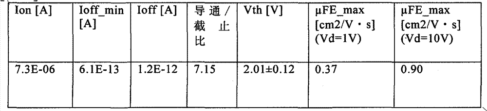
如上所述,通过相比于示例3增大半导体层115的厚度,载流子的传输量增加,而可以使导通电流及场效应迁移率增大。另外,由于相比于示例3半导体层115的厚度增大,导通电流增大而截止电流没有增大,所以通过使用在非晶结构中具有晶体区域的硅层作为缓冲层可以降低截止电流。另外,通过使用钛层作为与杂质半导体层接触的布线,与布线是钼层的示例2及示例3相比其接触电阻降低,所以可以使导通电流及场效应迁移率增大。As described above, by increasing the thickness of the
示例6Example 6
在本示例6中,将描述缓冲层与薄膜晶体管的截止电流之间的关系。在本示例中,将使用氨气作为缓冲层的源气体的薄膜晶体管和未使用氨气作为缓冲层的源气体的薄膜晶体管作比较。In this Example 6, the relationship between the buffer layer and the off-current of the thin film transistor will be described. In this example, a thin film transistor using ammonia gas as a source gas of the buffer layer and a thin film transistor not using ammonia gas as a source gas of the buffer layer were compared.
首先,将参照图15A至16C表示薄膜晶体管的制造工序。注意,样品1及样品2的缓冲层的沉积条件不同,但是其它条件都相同。First, the manufacturing process of the thin film transistor will be shown with reference to FIGS. 15A to 16C. Note that the deposition conditions of the buffer layer of
在衬底101上形成栅电极层103。A
与示例1同样地在衬底上形成厚度是150nm的钼层。接着,将抗蚀剂涂敷在钼层上,使用第一光掩模进行曝光并显影,来形成抗蚀剂掩模。A molybdenum layer with a thickness of 150 nm was formed on the substrate in the same manner as in Example 1. Next, a resist is applied on the molybdenum layer, exposed and developed using a first photomask, and a resist mask is formed.
接着,与示例1同样地使用该抗蚀剂掩模对钼层进行蚀刻,来形成栅电极层103。然后,去除抗蚀剂掩模。Next, in the same manner as in Example 1, the molybdenum layer was etched using this resist mask to form a
接着,在栅电极层103及衬底101上连续地形成栅极绝缘层107、半导体层109、缓冲层111及杂质半导体层113(参照图15A)。Next, a
在此,与示例2同样地层叠氮化硅层及氧化硅层作为栅极绝缘层107。Here, as in Example 2, a silicon nitride layer and a silicon oxide layer were stacked as the
接着,在与示例3同样的条件下在栅极绝缘层107上形成厚度是10nm的微晶硅层作为半导体层109。Next, a microcrystalline silicon layer having a thickness of 10 nm was formed as the
接着,在半导体层109上形成厚度是175nm的缓冲层作为缓冲层111。Next, a buffer layer having a thickness of 175 nm was formed on the
在样品1中,使用包含氨气的源气体形成缓冲层。此时的沉积条件如下:源气体为流量40sccm的SiH4、流量1475sccm的H2、流量25sccm的1000ppmNH3(氢稀释)及流量2000sccm的Ar,将处理室内的压力设定为280Pa,将衬底温度设定为280℃,并且将RF电源的功率设定为100W;在该条件下进行等离子体放电。In
在样品2中,使用不包含氨气的源气体形成缓冲层。此时的沉积条件如下:源气体为流量40sccm的SiH4、流量1500sccm的H2及流量是2000sccm的Ar,将处理室内的压力设定为280Pa,将衬底温度设定为280℃,并且将RF电源的功率设定为100W;在该条件下进行等离子体放电。即,在该条件下,从样品1的源气体中省去了氨气。In
接着,以与示例1同样的条件在缓冲层111上形成添加有磷的厚度是50nm的非晶硅层作为杂质半导体层113。Next, a phosphorus-doped amorphous silicon layer having a thickness of 50 nm was formed as the
接着,将抗蚀剂涂敷在杂质半导体层113上,然后使用第二光掩模进行曝光和显影,来形成抗蚀剂掩模。接着,使用该抗蚀剂掩模对半导体层109、缓冲层111及杂质半导体层113进行蚀刻,而形成半导体层115、缓冲层117及杂质半导体层119(参照图15B)。在此,使用与示例5同样的条件。然后,去除抗蚀剂掩模。Next, a resist is applied on the
接着,如图15C所示,形成导电层121以覆盖栅极绝缘层107、半导体层115、缓冲层117及杂质半导体层119。在此,在与示例1同样的条件形成厚度是300nm的钼层。Next, as shown in FIG. 15C , a
接着,将抗蚀剂涂敷在导电层121上,然后使用第三光掩模进行曝光和显影,来形成抗蚀剂掩模。如图16A所示,使用该抗蚀剂掩模对导电层121进行湿法蚀刻,来形成布线层123、125。注意,在本示例中,布线层123、125的平面形状均是线性的。Next, a resist is applied on the
接着,使用抗蚀剂掩模对杂质半导体层119进行蚀刻,来形成源区及漏区129。注意,在该工序中,缓冲层117的表面的一部分也被蚀刻而成为缓冲层131(参照图16B)。在此,使用与示例1同样的蚀刻条件。此时的缓冲层131的厚度为155nm。然后去除抗蚀剂掩模。Next, the
接着,用氟化碳等离子体辐照缓冲层131、源区及漏区129的表面,并去除残留在缓冲层131中的杂质。在此,在与示例5同样的条件下去除残留在缓冲层中的杂质。然后,对布线层123、125及缓冲层131的表面进行清洗。Next, the surfaces of the
接着,用水等离子体辐照缓冲层131、源区及漏区129的表面。在此,使用与示例2同样的条件。Next, the surfaces of the
接着,形成氮化硅层作为绝缘层133(参照图16C)。在此,在与示例1同样的条件形成厚度是300nm的氮化硅层。Next, a silicon nitride layer is formed as the insulating layer 133 (see FIG. 16C). Here, a silicon nitride layer having a thickness of 300 nm was formed under the same conditions as in Example 1.
接着,将抗蚀剂涂敷在绝缘层上,然后使用第四光掩模进行曝光和显影,来形成抗蚀剂掩模。使用该抗蚀剂掩模对绝缘层的一部分进行干法蚀刻,来使布线层125露出。另外,对绝缘层的一部分和栅极绝缘层107的一部分进行干法蚀刻,来使栅电极层103露出。在此,使用与示例1同样的蚀刻条件。然后,去除抗蚀剂掩模。Next, a resist is applied on the insulating layer, followed by exposure and development using a fourth photomask to form a resist mask. Using this resist mask, a part of the insulating layer is dry-etched to expose the
通过上述工序制造样品1及样品2的薄膜晶体管。Thin film transistors of
然后测量薄膜晶体管的电特性,且图47示出测量结果。此时,通过以0.25V增量增大栅极电压来执行测量。另外,进行测量时的温度为室温。注意,所制造的本示例的样品1和样品2的薄膜晶体管的沟道长度L为4μm,而沟道宽度W为20μm。在此,沟道宽度为栅电极的宽度。半导体层115的宽度是22μm。横轴表示漏极电压,纵轴表示漏极电流,并且在栅极电压设定为-5V、-10V、-15V的情况下,测量漏极电压是1V至30V时的漏极电流(在此为截止电流)。The electrical characteristics of the thin film transistor were then measured, and FIG. 47 shows the measurement results. At this time, measurement was performed by increasing the gate voltage in increments of 0.25V. In addition, the temperature at the time of measurement is room temperature. Note that the channel length L of the fabricated thin film transistors of
在图47中,实线471表示栅极电压是-5V时的样品1的薄膜晶体管的截止电流,实线473表示栅极电压是-10V时的样品1的薄膜晶体管的截止电流,并且实线475表示栅极电压是-15V时的样品1的薄膜晶体管的截止电流。另外,虚线477表示栅极电压是-5V时的样品2的薄膜晶体管的截止电流,虚线479表示栅极电压是-10V时的样品2的薄膜晶体管的截止电流,并且虚线481表示栅极电压是-15V时的样品2的薄膜晶体管的截止电流。In FIG. 47, the
根据图47,当在相同栅极电压下将样品1的截止电流与样品2的截止电流比较时,发现样品1中的截止电流更低。即,当使用利用氨气作为源气体形成的包含氮的在非晶结构中具有晶体区域的硅层被用作缓冲层时,截止电流降低。这是因为通过使用氨气作为缓冲层的源气体,可使缓冲层中的缺陷减少。According to FIG. 47 , when the off current of
示例7Example 7
在示例7中,将描述当在实施例1所描述的模拟中用NH基对晶粒界面中的Si的悬空键进行交联时的LUMO态。In Example 7, the LUMO state when the dangling bonds of Si in the grain interface are crosslinked with NH groups in the simulation described in Example 1 will be described.
图5及图6分别表示使用O原子对Si的晶粒界面处的悬空键进行交联的模型(模型1)和使用NH基对Si的晶粒界面处的悬空键进行交联的模型(模型2)中的LUMO(最低未占据分子轨道)态。在此,LUMO是处于激发状态的电子进入的最低能量的分子轨道,其与能带理论中的导带(CB)下缘的轨道相对应。因此,LUMO可以解释为有助于载流子传输的电子的波函数,和确定载流子迁移率的轨道。Fig. 5 and Fig. 6 respectively represent the model (model 1) that uses O atom to cross-link the dangling bond at the crystal grain interface of Si and the model (model 1) that uses NH group to cross-link the dangling bond at the Si grain interface. LUMO (lowest unoccupied molecular orbital) state in 2). Here, LUMO is the lowest energy molecular orbital into which electrons in an excited state enter, which corresponds to the orbital at the lower edge of the conduction band (CB) in the energy band theory. Therefore, LUMO can be interpreted as the wave function of electrons that contribute to carrier transport, and the orbitals that determine carrier mobility.
接着,调查模型1及模型2中的LUMO来自哪个原子和原子的哪个轨道。LUMO的波函数可以表示为膜中包括的原子的原子轨道的线性组合(就是,纯量倍数的和)。Next, investigate which atom and which orbital of the atom the LUMO in
注意,根据线性组合中的轨道各自的系数的绝对值的平方可获得Si原子轨道、H原子轨道、O原子轨道及N原子轨道中的每一个的存在概率,并且符号表示各原子轨道彼此具有键合性(相同符号)还是具有反键合性(不同符号)。Note that the existence probability of each of the Si atomic orbital, H atomic orbital, O atomic orbital, and N atomic orbital can be obtained from the square of the absolute value of the respective coefficients of the orbitals in the linear combination, and the symbol indicates that each atomic orbital has a bond with each other bonded (same symbol) or antibonded (different symbol).
接着,图43A表示在模型1的晶粒界面附近构成LUMO的主要原子轨道的示意图,而图43B表示在模型2的晶粒界面附近构成LUMO的主要原子轨道的示意图。在此,阴影线不同的区域具有相反符号的波函数。在此,示出了Si原子的s轨道452和456、Si原子的p轨道451、453、455和457,O原子的2s轨道454、N原子的2s轨道458、H原子的1s轨道459。Next, FIG. 43A shows a schematic diagram of the main atomic orbitals constituting the LUMO in the vicinity of the grain boundaries of
如图43A所示,在使用O原子对Si的晶粒界面处的悬空键进行交联的情况下,当O原子的2s轨道454聚集时,O原子的2s轨道454的位相与晶粒界面两侧的Si原子的sp3轨道(3s轨道452+3p轨道453和3s轨道456+3p轨道455)的位相不同。换言之,O原子的2s轨道454有助于原子之间的键合,但是因为其波函数的扩展窄,所以O原子的2s轨道454不能够连接电子云。因此,可以认为O原子的2s轨道454无助于提高导电率。As shown in FIG. 43A , in the case of using O atoms to cross-link the dangling bonds at the grain interfaces of Si, when the 2s orbitals 454 of O atoms gather, the phases of the 2s orbitals 454 of O atoms are two phases from the grain interfaces. The phases of the sp 3 orbitals (3s orbital 452+3p orbital 453 and 3s orbital 456+3p orbital 455 ) of the side Si atoms are different. In other words, the 2s orbital 454 of the O atom contributes to the bonding between atoms, but because the spread of its wave function is narrow, the 2s orbital 454 of the O atom cannot connect the electron cloud. Therefore, it can be considered that the 2s orbital 454 of the O atom does not contribute to the improvement of the conductivity.
另一方面,如图43B所示那样,在使用NH基对Si的晶粒界面的悬空键进行交联的情况下,当N原子的2s轨道458聚集时,N原子的2s轨道458的位相与晶粒界面两侧的Si原子的sp3轨道(3s轨道452+3p轨道453和3s轨道456+3p轨道455)的位相不同。换言之,N原子的2s轨道458不能够连接电子云。但是,通过将N原子的2s轨道458与H原子的1s轨道459混合,相同符号的区域,即Si原子的sp3轨道(3s轨道452+3p轨道453)、H原子的1s轨道459及Si的sp3轨道(3s轨道456+3p轨道455)成为键合性轨道,由此电子云能够彼此连接。从而,可以认为导电率提高。On the other hand, as shown in FIG. 43B , in the case of crosslinking the dangling bonds at the crystal grain interface of Si using NH groups, when the 2s orbitals 458 of N atoms are gathered, the phase of the 2s orbitals 458 of N atoms is the same as that of The phases of the sp 3 orbitals (3s orbital 452+3p orbital 453 and 3s orbital 456+3p orbital 455 ) of Si atoms on both sides of the grain interface are different. In other words, the 2s orbital 458 of the N atom cannot connect the electron cloud. However, by mixing the 2s orbital 458 of the N atom and the 1s orbital 459 of the H atom, the region of the same sign, that is, the sp 3 orbital of the Si atom (3s orbital 452 + 3p orbital 453), the 1s orbital 459 of the H atom, and the Si orbital The sp 3 orbital (3s orbital 456+3p orbital 455) becomes a bonding orbital, whereby electron clouds can be connected to each other. Accordingly, it is considered that the electrical conductivity is improved.
以上的结果可以如下地解释。即,因为LUMO处于激发状态(能量高),所以一般而言,LUMO具有如图44A所示的原子轨道的反键合性轨道。在如图43A的模型1所示的使用O原子在Si的晶粒界面处的交联,或者如图43B的模型2所示的使用NH基在Si的晶粒界面处的交联中,O原子及N原子的2s轨道454、458与Si原子的sp3轨道(3s轨道452+3p轨道453和3s轨道456+3p轨道455)具有反键合性(位相相反)。反键合性轨道是指在电子云之间形成接合。因此,在图43A的模型1所示的使用O原子在Si的晶粒界面处进行交联的情况下,电子云彼此不连接。同时,在如图43B的模型2所示的使用NH基在Si的晶粒界面处进行交联的情况下,虽然N原子的2s轨道458和Si的sp3轨道(3s轨道452+3p轨道453和3s轨道456+3p轨道455)形成反键合性轨道,但是因为存在有H原子,所以H原子的1s轨道459和Si的sp3轨道(3s轨道452+3p轨道453和3s轨道456+3p轨道455)可如图44B所示形成键合性轨道。换言之,因为在NH基中存在有H原子,所以电子云可相互连接。The above results can be explained as follows. That is, since LUMO is in an excited state (high energy), generally, LUMO has an antibonding orbital of an atomic orbital as shown in FIG. 44A . In the crosslinking at the grain boundary of Si using O atoms as shown in
注意,虽然CH2基具有H,但是因为CH2基中的C原子或H原子的原子轨道键合的分子轨道是具有更高能量的分子轨道,所以该分子轨道不包括在构成LUMO(最低未占据分子轨道)的原子轨道中。因此,可以认为即使通过使用CH2基在Si的晶粒界面处进行交联,电子云也不相互连接。Note that although the CH2 group has H, because the molecular orbital bonded to the atomic orbital of the C atom or the H atom in the CH2 group is a molecular orbital with higher energy, this molecular orbital is not included in the composition of the LUMO (lowest unidentified Occupying molecular orbitals) in atomic orbitals. Therefore, it can be considered that the electron clouds are not connected to each other even if crosslinking is performed at the grain interface of Si by using CH2 groups.
如上所述,在使用NH基交联悬空键的Si的晶粒界面的LUMO中,晶粒界面两端的Si原子的sp3轨道与N原子的2s轨道具有相反位相,但是其与H原子的1s轨道具有相同位相。因此,H原子的1s轨道起电子云之间的桥梁的作用。其结果是,电子云相互连接,从而形成载流子的通路。另外,可以预料到:为了连接Si的晶粒界面处的电子云,需要交联基中的原子轨道具有形成LUMO的原子(例如,O交联中的O原子、或NH基中的N原子和H原子)并具有与Si的sp3轨道相同位相的原子(例如,NH基中的H原子)。As described above, in the LUMO of the grain interface of Si using NH-based cross-linked dangling bonds, the sp 3 orbitals of the Si atoms at both ends of the grain interface have opposite phases to the 2s orbitals of the N atoms, but they have opposite phases to the 1s orbitals of the H atoms. orbitals have the same phase. Therefore, the 1s orbital of the H atom acts as a bridge between electron clouds. As a result, the electron clouds are connected to each other, thus forming a pathway for the charge carriers. In addition, it can be expected that in order to connect the electron cloud at the grain interface of Si, the atomic orbitals in the crosslinking group need to have atoms that form LUMOs (for example, O atoms in O crosslinking, or N atoms and H atom) and has the same phase as the sp 3 orbital of Si (for example, the H atom in the NH group).
本申请分别基于2008年6月27日、2009年2月27日和2009年5月28日向日本专利局提交的日本专利申请序列号2008-169286、2009-046433和2009-129313,上述申请的全部内容通过引用包括在本说明书中。This application is based on Japanese patent application serial numbers 2008-169286, 2009-046433, and 2009-129313 filed with the Japan Patent Office on June 27, 2008, February 27, 2009, and May 28, 2009, respectively, all of which The contents are included in this specification by reference.
Claims (30)
Applications Claiming Priority (7)
| Application Number | Priority Date | Filing Date | Title |
|---|---|---|---|
| JP2008-169286 | 2008-06-27 | ||
| JP2008169286 | 2008-06-27 | ||
| JP2009-046433 | 2009-02-27 | ||
| JP2009046433 | 2009-02-27 | ||
| JP2009-129313 | 2009-05-28 | ||
| JP2009129313 | 2009-05-28 | ||
| PCT/JP2009/061795 WO2009157574A1 (en) | 2008-06-27 | 2009-06-22 | Thin film transistor |
Publications (2)
| Publication Number | Publication Date |
|---|---|
| CN102077331A CN102077331A (en) | 2011-05-25 |
| CN102077331B true CN102077331B (en) | 2014-05-07 |
Family
ID=41444634
Family Applications (1)
| Application Number | Title | Priority Date | Filing Date |
|---|---|---|---|
| CN200980124705.1A Expired - Fee Related CN102077331B (en) | 2008-06-27 | 2009-06-22 | Thin film transistor |
Country Status (7)
| Country | Link |
|---|---|
| US (1) | US8637866B2 (en) |
| EP (1) | EP2291856A4 (en) |
| JP (1) | JP5448603B2 (en) |
| KR (1) | KR101703511B1 (en) |
| CN (1) | CN102077331B (en) |
| TW (1) | TWI460863B (en) |
| WO (1) | WO2009157574A1 (en) |
Families Citing this family (63)
| Publication number | Priority date | Publication date | Assignee | Title |
|---|---|---|---|---|
| JP5436017B2 (en) | 2008-04-25 | 2014-03-05 | 株式会社半導体エネルギー研究所 | Semiconductor device |
| JP5518366B2 (en) * | 2008-05-16 | 2014-06-11 | 株式会社半導体エネルギー研究所 | Thin film transistor |
| WO2009157573A1 (en) | 2008-06-27 | 2009-12-30 | Semiconductor Energy Laboratory Co., Ltd. | Thin film transistor, semiconductor device and electronic device |
| US8284142B2 (en) * | 2008-09-30 | 2012-10-09 | Semiconductor Energy Laboratory Co., Ltd. | Display device |
| JP5498762B2 (en) * | 2008-11-17 | 2014-05-21 | 株式会社半導体エネルギー研究所 | Method for manufacturing thin film transistor |
| US8530897B2 (en) * | 2008-12-11 | 2013-09-10 | Semiconductor Energy Laboratory Co., Ltd. | Display device including an inverter circuit having a microcrystalline layer |
| US7989325B2 (en) * | 2009-01-13 | 2011-08-02 | Semiconductor Energy Laboratory Co., Ltd. | Method for manufacturing crystalline semiconductor film and method for manufacturing thin film transistor |
| WO2010103906A1 (en) | 2009-03-09 | 2010-09-16 | Semiconductor Energy Laboratory Co., Ltd. | Thin film transistor |
| US9312156B2 (en) * | 2009-03-27 | 2016-04-12 | Semiconductor Energy Laboratory Co., Ltd. | Thin film transistor |
| JP5888802B2 (en) | 2009-05-28 | 2016-03-22 | 株式会社半導体エネルギー研究所 | Device having a transistor |
| US8772627B2 (en) * | 2009-08-07 | 2014-07-08 | Semiconductor Energy Laboratory Co., Ltd. | Photoelectric conversion device and manufacturing method thereof |
| JP5466933B2 (en) * | 2009-12-03 | 2014-04-09 | 株式会社ジャパンディスプレイ | Thin film transistor and manufacturing method thereof |
| KR101836067B1 (en) | 2009-12-21 | 2018-03-08 | 가부시키가이샤 한도오따이 에네루기 켄큐쇼 | Thin film transistor and manufacturing method thereof |
| TWI535028B (en) | 2009-12-21 | 2016-05-21 | 半導體能源研究所股份有限公司 | Thin film transistor |
| US8476744B2 (en) | 2009-12-28 | 2013-07-02 | Semiconductor Energy Laboratory Co., Ltd. | Thin film transistor with channel including microcrystalline and amorphous semiconductor regions |
| US8383434B2 (en) * | 2010-02-22 | 2013-02-26 | Semiconductor Energy Laboratory Co., Ltd. | Thin film transistor and manufacturing method thereof |
| US8830278B2 (en) | 2010-04-09 | 2014-09-09 | Semiconductor Energy Laboratory Co., Ltd. | Liquid crystal display device and method for driving the same |
| CN102834861B (en) | 2010-04-09 | 2016-02-10 | 株式会社半导体能源研究所 | The method of liquid crystal display and this liquid crystal display of driving |
| JPWO2011141949A1 (en) * | 2010-05-10 | 2013-07-22 | パナソニック株式会社 | Method for manufacturing crystalline semiconductor film, substrate with crystalline semiconductor film, thin film transistor |
| JP5933188B2 (en) * | 2010-05-14 | 2016-06-08 | 株式会社半導体エネルギー研究所 | Microcrystalline silicon film, manufacturing method thereof, and semiconductor device |
| KR101758297B1 (en) | 2010-06-04 | 2017-07-26 | 가부시키가이샤 한도오따이 에네루기 켄큐쇼 | Display device and electronic device |
| WO2011158948A1 (en) | 2010-06-18 | 2011-12-22 | Semiconductor Energy Laboratory Co., Ltd. | Method of manufacturing power storage device |
| US8564529B2 (en) | 2010-06-21 | 2013-10-22 | Semiconductor Energy Laboratory Co., Ltd. | Method for driving liquid crystal display device |
| US9286848B2 (en) | 2010-07-01 | 2016-03-15 | Semiconductor Energy Laboratory Co., Ltd. | Method for driving liquid crystal display device |
| TWI541782B (en) | 2010-07-02 | 2016-07-11 | 半導體能源研究所股份有限公司 | Liquid crystal display device |
| US8988337B2 (en) | 2010-07-02 | 2015-03-24 | Semiconductor Energy Laboratory Co., Ltd. | Driving method of liquid crystal display device |
| WO2012002165A1 (en) | 2010-07-02 | 2012-01-05 | Semiconductor Energy Laboratory Co., Ltd. | Liquid crystal display device and method for driving liquid crystal display device |
| US9336739B2 (en) | 2010-07-02 | 2016-05-10 | Semiconductor Energy Laboratory Co., Ltd. | Liquid crystal display device |
| TWI606490B (en) | 2010-07-02 | 2017-11-21 | 半導體能源研究所股份有限公司 | Semiconductor film manufacturing method, semiconductor device manufacturing method, and photoelectric conversion device manufacturing method |
| JP2012048220A (en) | 2010-07-26 | 2012-03-08 | Semiconductor Energy Lab Co Ltd | Liquid crystal display device and its driving method |
| JP5825895B2 (en) | 2010-08-06 | 2015-12-02 | 株式会社半導体エネルギー研究所 | Liquid crystal display |
| JP5948025B2 (en) * | 2010-08-06 | 2016-07-06 | 株式会社半導体エネルギー研究所 | Liquid crystal display |
| US8704230B2 (en) | 2010-08-26 | 2014-04-22 | Semiconductor Energy Laboratory Co., Ltd. | Semiconductor device and manufacturing method thereof |
| US9230826B2 (en) | 2010-08-26 | 2016-01-05 | Semiconductor Energy Laboratory Co., Ltd. | Etching method using mixed gas and method for manufacturing semiconductor device |
| US8643580B2 (en) | 2010-08-31 | 2014-02-04 | Semiconductor Energy Laboratory Co., Ltd. | Method for driving liquid crystal display device |
| TWI538218B (en) | 2010-09-14 | 2016-06-11 | 半導體能源研究所股份有限公司 | Thin film transistor |
| US8338240B2 (en) | 2010-10-01 | 2012-12-25 | Semiconductor Energy Laboratory Co., Ltd. | Method for manufacturing transistor |
| KR20120044042A (en) * | 2010-10-27 | 2012-05-07 | 삼성모바일디스플레이주식회사 | Organic light emitting display device and method for manufacturing the same |
| US8730416B2 (en) | 2010-12-17 | 2014-05-20 | Semiconductor Energy Laboratory Co., Ltd. | Liquid crystal display device |
| CN102096228B (en) * | 2010-12-17 | 2012-07-04 | 湖南创图视维科技有限公司 | Display system and display method |
| US9048327B2 (en) * | 2011-01-25 | 2015-06-02 | Semiconductor Energy Laboratory Co., Ltd. | Microcrystalline semiconductor film, method for manufacturing the same, and method for manufacturing semiconductor device |
| US9167234B2 (en) | 2011-02-14 | 2015-10-20 | Semiconductor Energy Laboratory Co., Ltd. | Display device |
| WO2012111427A1 (en) | 2011-02-16 | 2012-08-23 | Semiconductor Energy Laboratory Co., Ltd. | Display device |
| US9035860B2 (en) | 2011-02-16 | 2015-05-19 | Semiconductor Energy Laboratory Co., Ltd. | Display device |
| US8629445B2 (en) | 2011-02-21 | 2014-01-14 | Semiconductor Energy Laboratory Co., Ltd. | Semiconductor device, manufacturing method thereof, and electronic appliance |
| US9443455B2 (en) | 2011-02-25 | 2016-09-13 | Semiconductor Energy Laboratory Co., Ltd. | Display device having a plurality of pixels |
| US8994763B2 (en) | 2011-03-25 | 2015-03-31 | Semiconductor Energy Laboratory Co., Ltd. | Display device and driving method of the same |
| US9024927B2 (en) | 2011-06-15 | 2015-05-05 | Semiconductor Energy Laboratory Co., Ltd. | Display device and method for driving the same |
| US8988411B2 (en) | 2011-07-08 | 2015-03-24 | Semiconductor Energy Laboratory Co., Ltd. | Display device |
| JP6178050B2 (en) | 2011-07-15 | 2017-08-09 | 株式会社半導体エネルギー研究所 | Display device |
| KR20130010834A (en) | 2011-07-19 | 2013-01-29 | 가부시키가이샤 한도오따이 에네루기 켄큐쇼 | Display device |
| JP5998397B2 (en) * | 2011-10-25 | 2016-09-28 | 株式会社Joled | Thin film semiconductor device and manufacturing method thereof |
| KR20150011472A (en) | 2013-07-23 | 2015-02-02 | 삼성디스플레이 주식회사 | Thin film transistor and method of manufacturing the same |
| KR102245780B1 (en) | 2014-11-03 | 2021-04-29 | 삼성디스플레이 주식회사 | Laser crystallization system and laser crystallizatio method using the same, and display method using the same |
| KR102365963B1 (en) * | 2015-06-23 | 2022-02-23 | 삼성디스플레이 주식회사 | Thin film transistor, method of manufacturing the same and liquid crystal display apparatus having the same |
| CN105826398A (en) * | 2016-06-15 | 2016-08-03 | 京东方科技集团股份有限公司 | Thin film transistor, array substrate and manufacturing method |
| CN105870203B (en) * | 2016-06-24 | 2019-05-10 | 京东方科技集团股份有限公司 | A kind of thin film transistor and its preparation method, array substrate, display device |
| CN109728098B (en) * | 2019-01-03 | 2022-05-17 | 合肥鑫晟光电科技有限公司 | Thin film transistor, sensor, detection method, detection device and detection system |
| JP2021002633A (en) * | 2019-06-25 | 2021-01-07 | 日新電機株式会社 | Oxide semiconductor processing method and thin film transistor manufacturing method |
| US10964811B2 (en) | 2019-08-09 | 2021-03-30 | Micron Technology, Inc. | Transistor and methods of forming transistors |
| US11024736B2 (en) | 2019-08-09 | 2021-06-01 | Micron Technology, Inc. | Transistor and methods of forming integrated circuitry |
| US11637175B2 (en) * | 2020-12-09 | 2023-04-25 | Micron Technology, Inc. | Vertical transistors |
| CN115458588B (en) * | 2022-09-23 | 2026-01-23 | 武汉华星光电技术有限公司 | Display panel |
Citations (3)
| Publication number | Priority date | Publication date | Assignee | Title |
|---|---|---|---|---|
| EP0535979A2 (en) * | 1991-10-02 | 1993-04-07 | Sharp Kabushiki Kaisha | A thin film transistor and a method for producing the same |
| US5677236A (en) * | 1995-02-24 | 1997-10-14 | Mitsui Toatsu Chemicals, Inc. | Process for forming a thin microcrystalline silicon semiconductor film |
| JP2008124392A (en) * | 2006-11-15 | 2008-05-29 | Sharp Corp | Semiconductor device, manufacturing method thereof, and display device |
Family Cites Families (62)
| Publication number | Priority date | Publication date | Assignee | Title |
|---|---|---|---|---|
| JPS56122123A (en) | 1980-03-03 | 1981-09-25 | Shunpei Yamazaki | Semiamorphous semiconductor |
| US5091334A (en) | 1980-03-03 | 1992-02-25 | Semiconductor Energy Laboratory Co., Ltd. | Semiconductor device |
| JPS5771126A (en) | 1980-10-21 | 1982-05-01 | Semiconductor Energy Lab Co Ltd | Semiamorhous semiconductor |
| JPS5892217A (en) | 1981-11-28 | 1983-06-01 | Semiconductor Energy Lab Co Ltd | Manufacture of semiconductor device |
| JPS5972781A (en) | 1982-10-20 | 1984-04-24 | Semiconductor Energy Lab Co Ltd | Photoelectric conversion semiconductor device |
| JPS60160170A (en) | 1984-01-31 | 1985-08-21 | Seiko Instr & Electronics Ltd | thin film transistor |
| US5221631A (en) | 1989-02-17 | 1993-06-22 | International Business Machines Corporation | Method of fabricating a thin film transistor having a silicon carbide buffer layer |
| JP2839529B2 (en) | 1989-02-17 | 1998-12-16 | 株式会社東芝 | Thin film transistor |
| JPH03278466A (en) * | 1990-03-27 | 1991-12-10 | Toshiba Corp | Thin film transistor and manufacture thereof |
| US5514879A (en) | 1990-11-20 | 1996-05-07 | Semiconductor Energy Laboratory Co., Ltd. | Gate insulated field effect transistors and method of manufacturing the same |
| US5849601A (en) | 1990-12-25 | 1998-12-15 | Semiconductor Energy Laboratory Co., Ltd. | Electro-optical device and method for manufacturing the same |
| KR950013784B1 (en) | 1990-11-20 | 1995-11-16 | 가부시키가이샤 한도오따이 에네루기 겐큐쇼 | Field effect trasistor and its making method and tft |
| US7115902B1 (en) | 1990-11-20 | 2006-10-03 | Semiconductor Energy Laboratory Co., Ltd. | Electro-optical device and method for manufacturing the same |
| KR920010885A (en) * | 1990-11-30 | 1992-06-27 | 카나이 쯔또무 | Thin film semiconductor, manufacturing method and manufacturing apparatus and image processing apparatus |
| US7098479B1 (en) | 1990-12-25 | 2006-08-29 | Semiconductor Energy Laboratory Co., Ltd. | Electro-optical device and method for manufacturing the same |
| JPH04266019A (en) * | 1991-02-20 | 1992-09-22 | Canon Inc | Film formation |
| JP3255942B2 (en) | 1991-06-19 | 2002-02-12 | 株式会社半導体エネルギー研究所 | Method for manufacturing inverted staggered thin film transistor |
| JPH05129608A (en) | 1991-10-31 | 1993-05-25 | Sharp Corp | Semiconductor device |
| US6835523B1 (en) | 1993-05-09 | 2004-12-28 | Semiconductor Energy Laboratory Co., Ltd. | Apparatus for fabricating coating and method of fabricating the coating |
| JPH06326312A (en) | 1993-05-14 | 1994-11-25 | Toshiba Corp | Active matrix display device |
| US5932302A (en) | 1993-07-20 | 1999-08-03 | Semiconductor Energy Laboratory Co., Ltd. | Method for fabricating with ultrasonic vibration a carbon coating |
| JPH07131030A (en) | 1993-11-05 | 1995-05-19 | Sony Corp | Display thin film semiconductor device and manufacturing method thereof |
| TW303526B (en) | 1994-12-27 | 1997-04-21 | Matsushita Electric Industrial Co Ltd | |
| JP2661594B2 (en) * | 1995-05-25 | 1997-10-08 | 日本電気株式会社 | Thin film transistor and method of manufacturing the same |
| US6035101A (en) * | 1997-02-12 | 2000-03-07 | Applied Materials, Inc. | High temperature multi-layered alloy heater assembly and related methods |
| US5920772A (en) | 1997-06-27 | 1999-07-06 | Industrial Technology Research Institute | Method of fabricating a hybrid polysilicon/amorphous silicon TFT |
| US6372535B1 (en) * | 1998-02-02 | 2002-04-16 | Samsung Electronics Co., Ltd. | Manufacturing method of a thin film transistor |
| JP4458563B2 (en) * | 1998-03-31 | 2010-04-28 | 三菱電機株式会社 | Thin film transistor manufacturing method and liquid crystal display device manufacturing method using the same |
| JP2000277439A (en) | 1999-03-25 | 2000-10-06 | Kanegafuchi Chem Ind Co Ltd | Plasma CVD method of crystalline silicon thin film and method of manufacturing silicon thin film photoelectric conversion device |
| JP2001007024A (en) | 1999-06-18 | 2001-01-12 | Sanyo Electric Co Ltd | Method of forming of polycrystalline silicon film |
| JP2001053283A (en) | 1999-08-12 | 2001-02-23 | Semiconductor Energy Lab Co Ltd | Semiconductor device and manufacturing method thereof |
| JP2001102587A (en) | 1999-09-28 | 2001-04-13 | Toshiba Corp | Thin film transistor, method of manufacturing the same, and method of manufacturing a semiconductor thin film |
| JP2001196598A (en) * | 1999-10-29 | 2001-07-19 | Hitachi Ltd | Semiconductor device, manufacturing method thereof, and liquid crystal display device |
| JP3792589B2 (en) * | 2001-03-29 | 2006-07-05 | 富士通株式会社 | Manufacturing method of semiconductor device |
| JP2002299235A (en) * | 2001-03-30 | 2002-10-11 | Matsushita Electric Ind Co Ltd | Semiconductor thin film forming method and thin film semiconductor device |
| JP4860055B2 (en) * | 2001-05-31 | 2012-01-25 | 株式会社半導体エネルギー研究所 | Method for manufacturing semiconductor device |
| KR100421480B1 (en) * | 2001-06-01 | 2004-03-12 | 엘지.필립스 엘시디 주식회사 | Method for Processing Surface of Organic Isolation Film and Method of Fabricating Thin Film Transistor Substate using the same |
| KR100436181B1 (en) | 2002-04-16 | 2004-06-12 | 엘지.필립스 엘시디 주식회사 | method for fabricating of an array substrate for a liquid crystal display device |
| JP2004014958A (en) | 2002-06-11 | 2004-01-15 | Fuji Electric Holdings Co Ltd | Thin film polycrystalline solar cell and method of manufacturing the same |
| US6841431B2 (en) * | 2003-01-29 | 2005-01-11 | Chunghwa Picture Tubes, Ltd. | Method for reducing the contact resistance |
| CN100552893C (en) * | 2003-03-26 | 2009-10-21 | 株式会社半导体能源研究所 | Semiconductor device and manufacturing method thereof |
| JP4108633B2 (en) * | 2003-06-20 | 2008-06-25 | シャープ株式会社 | THIN FILM TRANSISTOR, MANUFACTURING METHOD THEREOF, AND ELECTRONIC DEVICE |
| TWI399580B (en) | 2003-07-14 | 2013-06-21 | 半導體能源研究所股份有限公司 | Semiconductor device and display device |
| JP4748954B2 (en) | 2003-07-14 | 2011-08-17 | 株式会社半導体エネルギー研究所 | Liquid crystal display |
| JP2005050905A (en) | 2003-07-30 | 2005-02-24 | Sharp Corp | Method for manufacturing silicon thin film solar cell |
| TWI372463B (en) | 2003-12-02 | 2012-09-11 | Semiconductor Energy Lab | Laser irradiation apparatus, laser irradiation method, and method for manufacturing semiconductor device |
| JP5159021B2 (en) | 2003-12-02 | 2013-03-06 | 株式会社半導体エネルギー研究所 | Method for manufacturing semiconductor device |
| JP2005167051A (en) | 2003-12-04 | 2005-06-23 | Sony Corp | THIN FILM TRANSISTOR AND METHOD FOR PRODUCING THIN FILM TRANSISTOR |
| KR100724485B1 (en) * | 2005-04-19 | 2007-06-04 | 엘지.필립스 엘시디 주식회사 | Method of manufacturing thin film transistor of liquid crystal display |
| JP4266019B2 (en) | 2005-08-30 | 2009-05-20 | 本田技研工業株式会社 | Injection mold hot runner mold color changing device |
| KR100722085B1 (en) * | 2005-09-12 | 2007-05-25 | 삼성전자주식회사 | Solar cell comprising carbon nanotubes formed by electrophoresis and a method of manufacturing the same |
| KR100978260B1 (en) * | 2005-12-27 | 2010-08-26 | 엘지디스플레이 주식회사 | LCD and its manufacturing method |
| US20080035306A1 (en) * | 2006-08-08 | 2008-02-14 | White John M | Heating and cooling of substrate support |
| JP5331389B2 (en) | 2007-06-15 | 2013-10-30 | 株式会社半導体エネルギー研究所 | Method for manufacturing display device |
| CN102007585B (en) | 2008-04-18 | 2013-05-29 | 株式会社半导体能源研究所 | Thin film transistor and manufacturing method thereof |
| JP5416460B2 (en) | 2008-04-18 | 2014-02-12 | 株式会社半導体エネルギー研究所 | Thin film transistor and method for manufacturing thin film transistor |
| WO2009128522A1 (en) | 2008-04-18 | 2009-10-22 | Semiconductor Energy Laboratory Co., Ltd. | Thin film transistor and method for manufacturing the same |
| US8053294B2 (en) | 2008-04-21 | 2011-11-08 | Semiconductor Energy Laboratory Co., Ltd. | Manufacturing method of thin film transistor by controlling generation of crystal nuclei of microcrystalline semiconductor film |
| US8049215B2 (en) | 2008-04-25 | 2011-11-01 | Semiconductor Energy Laboratory Co., Ltd. | Thin film transistor |
| JP5436017B2 (en) | 2008-04-25 | 2014-03-05 | 株式会社半導体エネルギー研究所 | Semiconductor device |
| JP5518366B2 (en) | 2008-05-16 | 2014-06-11 | 株式会社半導体エネルギー研究所 | Thin film transistor |
| WO2009157573A1 (en) | 2008-06-27 | 2009-12-30 | Semiconductor Energy Laboratory Co., Ltd. | Thin film transistor, semiconductor device and electronic device |
-
2009
- 2009-06-22 KR KR1020117002075A patent/KR101703511B1/en not_active Expired - Fee Related
- 2009-06-22 EP EP09770284.9A patent/EP2291856A4/en not_active Withdrawn
- 2009-06-22 CN CN200980124705.1A patent/CN102077331B/en not_active Expired - Fee Related
- 2009-06-22 WO PCT/JP2009/061795 patent/WO2009157574A1/en not_active Ceased
- 2009-06-24 US US12/490,447 patent/US8637866B2/en not_active Expired - Fee Related
- 2009-06-26 JP JP2009152189A patent/JP5448603B2/en not_active Expired - Fee Related
- 2009-06-26 TW TW098121640A patent/TWI460863B/en not_active IP Right Cessation
Patent Citations (3)
| Publication number | Priority date | Publication date | Assignee | Title |
|---|---|---|---|---|
| EP0535979A2 (en) * | 1991-10-02 | 1993-04-07 | Sharp Kabushiki Kaisha | A thin film transistor and a method for producing the same |
| US5677236A (en) * | 1995-02-24 | 1997-10-14 | Mitsui Toatsu Chemicals, Inc. | Process for forming a thin microcrystalline silicon semiconductor film |
| JP2008124392A (en) * | 2006-11-15 | 2008-05-29 | Sharp Corp | Semiconductor device, manufacturing method thereof, and display device |
Also Published As
| Publication number | Publication date |
|---|---|
| EP2291856A4 (en) | 2015-09-23 |
| US20090321737A1 (en) | 2009-12-31 |
| US8637866B2 (en) | 2014-01-28 |
| CN102077331A (en) | 2011-05-25 |
| JP2011009506A (en) | 2011-01-13 |
| KR20110029157A (en) | 2011-03-22 |
| TW201013933A (en) | 2010-04-01 |
| WO2009157574A1 (en) | 2009-12-30 |
| TWI460863B (en) | 2014-11-11 |
| KR101703511B1 (en) | 2017-02-07 |
| JP5448603B2 (en) | 2014-03-19 |
| EP2291856A1 (en) | 2011-03-09 |
Similar Documents
| Publication | Publication Date | Title |
|---|---|---|
| CN102077331B (en) | Thin film transistor | |
| CN102007585B (en) | Thin film transistor and manufacturing method thereof | |
| US8513664B2 (en) | Thin film transistor, semiconductor device and electronic device | |
| CN102007586B (en) | Thin film transistor and method for manufacturing the same | |
| US8124972B2 (en) | Thin film transistor | |
| JP5416460B2 (en) | Thin film transistor and method for manufacturing thin film transistor | |
| KR101624484B1 (en) | Manufacturing method of transistor | |
| CN102386072B (en) | The manufacture method of microcrystalline semiconductor film and the manufacture method of semiconductor device | |
| KR20090057929A (en) | Microcrystalline semiconductor film, thin film transistor which has this microcrystalline semiconductor film, and manufacturing method of photoelectric conversion apparatus | |
| US8168973B2 (en) | Thin film transistor | |
| JP5436016B2 (en) | Semiconductor device | |
| JP5602389B2 (en) | Thin film transistor |
Legal Events
| Date | Code | Title | Description |
|---|---|---|---|
| C06 | Publication | ||
| PB01 | Publication | ||
| C10 | Entry into substantive examination | ||
| SE01 | Entry into force of request for substantive examination | ||
| C14 | Grant of patent or utility model | ||
| GR01 | Patent grant | ||
| CF01 | Termination of patent right due to non-payment of annual fee |
Granted publication date: 20140507 Termination date: 20190622 |
|
| CF01 | Termination of patent right due to non-payment of annual fee |