CN102051603B - Plasm-aided selenium sulfuration treatment device and process - Google Patents
Plasm-aided selenium sulfuration treatment device and process Download PDFInfo
- Publication number
- CN102051603B CN102051603B CN201010518539A CN201010518539A CN102051603B CN 102051603 B CN102051603 B CN 102051603B CN 201010518539 A CN201010518539 A CN 201010518539A CN 201010518539 A CN201010518539 A CN 201010518539A CN 102051603 B CN102051603 B CN 102051603B
- Authority
- CN
- China
- Prior art keywords
- selenium
- plasma
- plate
- vacuum chamber
- treatment device
- Prior art date
- Legal status (The legal status is an assumption and is not a legal conclusion. Google has not performed a legal analysis and makes no representation as to the accuracy of the status listed.)
- Expired - Fee Related
Links
Images


Classifications
-
- Y—GENERAL TAGGING OF NEW TECHNOLOGICAL DEVELOPMENTS; GENERAL TAGGING OF CROSS-SECTIONAL TECHNOLOGIES SPANNING OVER SEVERAL SECTIONS OF THE IPC; TECHNICAL SUBJECTS COVERED BY FORMER USPC CROSS-REFERENCE ART COLLECTIONS [XRACs] AND DIGESTS
- Y02—TECHNOLOGIES OR APPLICATIONS FOR MITIGATION OR ADAPTATION AGAINST CLIMATE CHANGE
- Y02P—CLIMATE CHANGE MITIGATION TECHNOLOGIES IN THE PRODUCTION OR PROCESSING OF GOODS
- Y02P70/00—Climate change mitigation technologies in the production process for final industrial or consumer products
- Y02P70/50—Manufacturing or production processes characterised by the final manufactured product
Landscapes
- Photovoltaic Devices (AREA)
Abstract
一种等离子体辅助硒硫化处理装置,设置于真空室内,包括壳体、阴极板和阳极板,阴极板和阳极板交替叠放形成等离子体发生器,阴极板设有固定半导体薄膜基板的沟槽,阳极板表面均布小孔并设有输气管、独立内加热电极和阳极测温点基于该处理装置的工艺为:1)在半导体薄膜材料上按化学式配比预制金属层,然后放入阴极板的沟槽中;2)将其置于真空室内抽真空,打开电源加热阴极板和阳极板,启动等离子体发生器电源,并通入硒或硫、氢、氩混合气体。本发明的优点:硒原子的反应活性高,金属预制层的硒化反应完全,光电转换效率高;基片的加热温度低,不易变形;采用电子方式监控两电极间容抗的变化,了解转化的进展,减少工业化生产的废品率。
A plasma-assisted selenium vulcanization treatment device, which is arranged in a vacuum chamber and includes a housing, a cathode plate and an anode plate, the cathode plates and the anode plates are alternately stacked to form a plasma generator, and the cathode plate is provided with a groove for fixing a semiconductor thin film substrate , the surface of the anode plate is evenly distributed with small holes and is provided with a gas delivery pipe, an independent internal heating electrode and an anode temperature measuring point. The process based on this processing device is: 1) Prefabricate a metal layer on the semiconductor film material according to the chemical formula ratio, and then put it into the cathode 2) Place it in a vacuum chamber to evacuate, turn on the power to heat the cathode plate and the anode plate, start the plasma generator power supply, and feed selenium or sulfur, hydrogen, argon mixed gas. The invention has the advantages of high reactivity of selenium atoms, complete selenization reaction of the metal prefabricated layer, high photoelectric conversion efficiency; low heating temperature of the substrate, not easily deformed; electronically monitors the change of the capacitive reactance between the two electrodes, and understands the transformation progress and reduce the scrap rate of industrial production.
Description
技术领域 technical field
本发明涉及太阳能电池薄膜材料制备技术,特别是一种等离子体辅助硒硫化处理装置及工艺。The invention relates to a solar cell film material preparation technology, in particular to a plasma-assisted selenium vulcanization treatment device and process.
背景技术 Background technique
铜铟硒(CuInSe2缩写为:CIS)或其中固溶镓、硫的铜铟镓硒[Cu(InGa)(SeS)2缩写为:CIGS]太阳薄膜电池是在普通钠钙玻璃或聚酰亚胺薄膜、金属薄板(铝、不锈钢、钼箔等)衬底上分别沉积多层薄膜而构成的光伏器件,其单体电池结构一般为:玻璃衬底/金属钼(Mo)背电极/光吸收层(CIGS)/缓冲层[CdS、ZnS、ZnSe、In(OH)3、ZnS(O,OH)等]/高阻本征i-ZnO/导电窗口层[掺杂ZnO(ZnO:Al、ZnO:Ga、ZnO:B)、SnO2、ITO(氧化铟锡)等]/金属栅状电极/减反射膜等组成。其中光学吸收层的CIGS薄膜制备的质量是阻碍电池产业化的主要困难之一;CIGS光学吸收层薄膜的制备工艺方法主要有:1)共蒸发法,它是将Cu、In、Ga和Se作源在真空室中进行反应共蒸发沉积在Mo背电极上,共蒸发法要求薄膜中各元素的蒸发速率和电池衬底的沉积量均要求精确控制,薄膜大面积沉积的均匀性和重现性要求很严,相应真空沉积设备控制精度和造价很高;2)金属预置层后硒硫化法,先在衬底上分别或混合溅射一定化学配比量的Cu、In、Ga金属预制层,再在真空热处理炉内与H2Se(H2S)或饱和硒蒸汽(或硫蒸汽)进行硒硫化反应,最终生成满足化学配比要求的Cu(In,Ga)Se2化合物半导体多晶薄膜;3)分层沉积Cu、In、Ga和Se或CuSe2、In2Se3、Ga2Se3分层沉积,再放入硒(或硫)气氛炉内快速热处理,转化成Cu(In,Ga)Se2化合物半导体多晶薄膜。Copper indium gallium selenide (CuInSe 2 abbreviated as: CIS) or copper indium gallium selenide [Cu(InGa) (SeS) 2 abbreviated as: CIGS] in which gallium and sulfur are solid-dissolved Photovoltaic devices composed of multi-layer thin films deposited on amine thin films and thin metal plates (aluminum, stainless steel, molybdenum foil, etc.) layer (CIGS)/buffer layer [CdS, ZnS, ZnSe, In(OH) 3 , ZnS(O, OH), etc.]/high resistance intrinsic i-ZnO/conductive window layer [doped ZnO(ZnO:Al, ZnO :Ga, ZnO:B), SnO 2 , ITO (indium tin oxide), etc.]/metal grid electrode/anti-reflection film, etc. Wherein the quality that the CIGS thin film of optical absorbing layer is prepared is one of main difficulty hindering battery industrialization; The preparation technology method of CIGS optical absorbing layer thin film mainly contains: 1) co-evaporation method, it is to use Cu, In, Ga and Se as The source is reacted in a vacuum chamber and co-evaporated and deposited on the Mo back electrode. The co-evaporation method requires precise control of the evaporation rate of each element in the film and the deposition amount of the battery substrate, and the uniformity and reproducibility of the large-area deposition of the film. The requirements are very strict, and the control accuracy and cost of the corresponding vacuum deposition equipment are very high; 2) Selenium vulcanization method after the metal pre-layer, firstly sputtering a certain stoichiometric amount of Cu, In, and Ga metal pre-layers on the substrate respectively or mixed , and then carry out selenium sulfidation reaction with H 2 Se (H 2 S) or saturated selenium vapor (or sulfur vapor) in a vacuum heat treatment furnace, and finally generate a Cu(In, Ga)Se 2 compound semiconductor polycrystalline film that meets the stoichiometric requirements; 3) layered deposition Cu, In, Ga and Se or CuSe 2 , In 2 Se 3 , Ga 2 Se 3 layered deposition, and then placed in a selenium (or sulfur) atmosphere furnace for rapid heat treatment, converted into Cu(In, Ga ) Se 2 compound semiconductor polycrystalline film.
共蒸发法是CIGS薄膜电池小面积高效率电池制作的主要方法,但是大面积产业化时均匀性差。The co-evaporation method is the main method for small-area high-efficiency CIGS thin-film battery manufacturing, but the uniformity is poor in large-area industrialization.
金属预制层后硒化法较易实现大面积制作CIGS薄膜电池组件,是一产业化的主要途径。金属预制层后硒硫化法有二种:一种是通入H2Se(H2Se+Ar)[或H2S(H2S+Ar)]气体进行化学气相反应形成CIGS薄膜;另一种是固态硒或硫加热气化后在较高温度下与预制层金属Cu、In和Ga发生化学反应形成CIGS薄膜。在H2Se气相硒化时,H2Se在预制层表面分解提供活性硒原子和活性氢原子,活性氢原子很容易在材料中渗透和扩散,相对金属原子,它易得到电子成为负离子,相对其它非金属原子,它易失去电子成为正离子。在金属预制层硒化的过程中,原子之间由金属键转变为共价健,键能增大,需要外界输入能量克服势垒和提供机会,氢原子提供了双性的氢键过渡,起到了传媒和催化的作用,加速了金属预制层转变成化合物半导体薄膜材料的过程,固态源硒化时,也可通入氢气,但氢分子要进入金属或化合物半导体中,必须先被材料表面活性点所吸附、分解成氢原子,才能起到传媒和催化作用。这种方法的特点是可以得到高质量的均匀的薄膜,但是H2Se气体属于剧毒危险品,易燃易爆,运输困难,价格昂贵,国内没有生产厂家,直接利用H2Se气体进行金属预制层后硒化制备CIGS薄膜材料较难实施。The selenization method after the metal prefabricated layer is easier to realize large-scale production of CIGS thin film battery components, which is the main way of industrialization. There are two selenium vulcanization methods after the metal prefabricated layer: one is to pass H 2 Se(H 2 Se+Ar)[or H 2 S(H 2 S+Ar)] gas for chemical gas phase reaction to form CIGS film; One is that solid selenium or sulfur is heated and vaporized to form a CIGS film by chemical reaction with prefabricated layer metal Cu, In and Ga at a higher temperature. During the gas-phase selenization of H 2 Se, H 2 Se decomposes on the surface of the prefabricated layer to provide active selenium atoms and active hydrogen atoms. The active hydrogen atoms are easy to penetrate and diffuse in the material. Compared with metal atoms, it is easy to obtain electrons and become negative ions. Other non-metal atoms, it is easy to lose electrons to become positive ions. During the selenization process of the metal prefabricated layer, the metal bond between the atoms is transformed into a covalent bond, and the bond energy increases, requiring external energy input to overcome the potential barrier and provide an opportunity. The hydrogen atom provides a double-character hydrogen bond transition, starting The role of media and catalysis accelerates the process of transforming the metal prefabricated layer into a compound semiconductor thin film material. When the solid source is selenized, hydrogen gas can also be introduced, but the hydrogen molecules must first be activated by the surface of the material to enter the metal or compound semiconductor. Only by absorbing and decomposing into hydrogen atoms, can it play the role of media and catalysis. The characteristic of this method is that high-quality uniform films can be obtained, but H 2 Se gas is highly toxic and dangerous, flammable and explosive, difficult to transport, and expensive. There is no domestic manufacturer, and H 2 Se gas is directly used for metal processing. It is difficult to prepare CIGS thin film materials by selenization after prefabricated layers.
固态源后硒硫化制备CIGS薄膜技术的设备较简单,能降低CIGS薄膜材料的制备成本,固态硒(或硫)原材料的毒性不大,易于实现工业化生产。但是它存在以下缺点:1).固态硒(或硫)源形成的气态硒大多以Se5、Se6、Se7等大分子团或原子簇形式存在,与H2Se相比,反应活性差、过程复杂,反应温度高,接近玻璃基片的软化点;2).由于固态源硒(或硫化)气化时,是从一定的位置产生气体,对于大面积的基片来说,不容易形成均匀分布,形成的薄膜均匀性很差,难以用于大面积的产业化;3).预制层金属Cu、In、Ga转变成化合物半导体薄膜材料时,几乎每个原子之间的相互关系都发生了变化,由原子间的金属键作用转变为共价键,另一方面,硒原子与金属预制层反应,其体积发生了变化,与Mo接触的界面发生了位移,造成CIGS薄膜与Mo背电极结合力严重下降,影响半导体薄膜电池下道工序进行和最终薄膜器件的质量;4).金属镓一般是以铜镓合金的形式与铟分别叠加溅射形成预制层,硒化时薄膜内金属铟比镓更容易反应,因而容易形成CuInSe2,而不是Cu(In,Ga)Se2,造成Ga原子被驱赶到底层,另一方面Ga更容易与Mo化合,Ga向Mo背电极扩散而不能形成化合物半导体,制备的半导体薄膜电池吸收层材料的禁带宽度比理论预期值低,电池开路电压和光电转化效率均不高。The equipment for preparing CIGS thin film technology by selenium vulcanization after solid source is relatively simple, which can reduce the preparation cost of CIGS thin film material. The toxicity of solid selenium (or sulfur) raw materials is not large, and it is easy to realize industrial production. But it has the following disadvantages: 1). The gaseous selenium formed by the solid selenium (or sulfur) source mostly exists in the form of macromolecular groups or atomic clusters such as Se 5 , Se 6 , and Se 7 , and has poor reactivity compared with H 2 Se , the process is complicated, the reaction temperature is high, and it is close to the softening point of the glass substrate; 2). Since the gasification of the solid source selenium (or sulfide) is generated from a certain position, it is not easy for a large-area substrate Form a uniform distribution, and the uniformity of the formed film is very poor, and it is difficult to be used for large-scale industrialization; 3). When the prefabricated layer metal Cu, In, and Ga are converted into compound semiconductor film materials, the relationship between almost every atom is very different. Changes have taken place, from the metal bond between atoms to the covalent bond, on the other hand, the selenium atom reacts with the metal prefabricated layer, its volume has changed, and the interface in contact with Mo has shifted, resulting in the CIGS film and the Mo back The electrode binding force is severely reduced, which affects the next process of semiconductor thin film batteries and the quality of the final thin film device; 4). Metal gallium is generally in the form of copper gallium alloy and indium is sputtered separately to form a prefabricated layer. During selenization, the metal in the film Indium is more reactive than gallium, so it is easy to form CuInSe 2 instead of Cu(In, Ga)Se 2 , causing Ga atoms to be driven to the bottom layer. On the other hand, Ga is more likely to combine with Mo, and Ga diffuses to the back electrode of Mo and cannot Forming compound semiconductors, the forbidden band width of the absorbing layer material of the prepared semiconductor thin film battery is lower than the theoretical expected value, and the open circuit voltage and photoelectric conversion efficiency of the battery are not high.
气相硒硫化与固态源硒硫化的共同缺点是薄膜结晶质量或结构疏松,致密性较差,半导体多晶薄膜的缺陷态很多,薄膜电池的光电转换效率较低。The common disadvantages of gas phase selenium sulfide and solid source selenium sulfide are that the crystal quality or structure of the film is loose, the compactness is poor, the semiconductor polycrystalline film has many defect states, and the photoelectric conversion efficiency of the thin film battery is low.
发明内容 Contents of the invention
本发明的目的是针对上述存在问题,提供一种等离子体辅助硒硫化处理装置及工艺,该装置设备简单、制备成本低,该工艺易于实施、制备的薄膜结晶致密度高、薄膜电池的光电转换效率高且制备过程安全可靠。The object of the present invention is to address the above-mentioned problems and provide a plasma-assisted selenium vulcanization treatment device and process. The device is simple in equipment and low in preparation cost. The efficiency is high and the preparation process is safe and reliable.
本发明的技术方案:Technical scheme of the present invention:
一种等离子体辅助硒硫化处理装置,设置于真空室内,包括壳体、阴极板和阳极板,壳体为长方体结构,设有两块侧板和底板,阴极板和阳极板在壳体内平行间隔交替叠放并固定在壳体的底板上,阴极板和阳极板交替叠放形成等离子体发生器,壳体的侧板即为等离子体发生器的外壳,阴极板设有固定半导体薄膜基板的沟槽,阴极板上设有均匀分布1~4个独立内加热电极和电池基片测温点,阳极板为腔体结构,阳极板表面均布小孔,孔径0.5mm~1.5mm,孔间距5mm~20mm,阳极板上设有输气管与腔体相通,阳极板上设有均匀分布1~3个独立内加热电极和阳极测温点,阴极板和阳极板分别设有极柱并与真空室外的等离子体发生电源连接,所述内加热电极、测温点和输气管分别与真空室外的加热电源、电路及气路连接,内加热电极与测温点通过自动控温系统PID形成闭环温度控制,气路上设有气体流量计。A plasma-assisted selenium vulcanization treatment device is arranged in a vacuum chamber and includes a housing, a cathode plate and an anode plate. The housing is a cuboid structure with two side plates and a bottom plate. The cathode plate and the anode plate are spaced apart in parallel in the housing. Alternately stacked and fixed on the bottom plate of the shell, the cathode plate and the anode plate are alternately stacked to form a plasma generator, the side plate of the shell is the shell of the plasma generator, and the cathode plate is provided with a groove for fixing the semiconductor thin film substrate The cathode plate is equipped with 1 to 4 independent internal heating electrodes and battery substrate temperature measuring points evenly distributed, the anode plate is a cavity structure, and the surface of the anode plate is evenly distributed with small holes, the hole diameter is 0.5mm ~ 1.5mm, and the hole spacing is 5mm ~20mm, the anode plate is equipped with a gas pipe to communicate with the cavity, the anode plate is equipped with 1 to 3 independent internal heating electrodes and anode temperature measuring points evenly distributed, the cathode plate and the anode plate are respectively equipped with poles and connected to the vacuum chamber The plasma generation power supply is connected, and the inner heating electrode, temperature measuring point and gas pipeline are respectively connected to the heating power supply, circuit and gas path outside the vacuum chamber. The inner heating electrode and temperature measuring point form a closed-loop temperature control through the automatic temperature control system PID , There is a gas flow meter on the gas line.
所述阴极板材质为W、Mo或Ta,数量为2~64片。The material of the cathode plate is W, Mo or Ta, and the quantity is 2-64 pieces.
所述阳极板材质为Mo金属薄板,数量为2~64片。The material of the anode plate is Mo metal thin plate, and the quantity is 2-64 pieces.
所述等离子体外壳设有2~4层保温套或热反射隔热板,其最内层材质是Mo金属薄板,其余各层材质为不锈钢薄板,等离子体外壳固定在真空室内并与真空室箱体形成等电位体。The plasma shell is provided with 2 to 4 layers of thermal insulation sleeves or heat-reflecting heat insulation boards, the innermost layer is made of Mo metal sheet, and the other layers are made of stainless steel sheets. The plasma shell is fixed in the vacuum chamber and connected with the vacuum chamber box. The body forms an equipotential body.
所述半导体薄膜基板在阴极板两端设为卷带式结构,以实现半导体薄膜基板在处理装置中的连续进给。The semiconductor thin film substrate is configured as a tape-and-roll structure at both ends of the cathode plate, so as to realize continuous feeding of the semiconductor thin film substrate in the processing device.
所述硒硫化处理装置为1~8个并分别按线形排列设置于相同数量的真空室内,每个真空室设有一个可在真空室中轴线方向运动的小车,按连续流水线方式实施。There are 1 to 8 selenium vulcanization devices and they are respectively arranged in the same number of vacuum chambers in a linear arrangement. Each vacuum chamber is provided with a trolley that can move in the direction of the central axis of the vacuum chamber, and is implemented in a continuous assembly line.
所述硒硫化处理装置为水平或垂直设置于真空室内。The selenium sulfide treatment device is installed horizontally or vertically in the vacuum chamber.
一种基于所述等离子体辅助硒硫化处理装置的工艺方法,步骤如下:A process method based on the plasma-assisted selenium vulcanization treatment device, the steps are as follows:
1)在半导体薄膜材料上按化学式配比预制金属层,然后放入阴极板的沟槽中;1) Prefabricate the metal layer on the semiconductor film material according to the chemical formula ratio, and then put it into the groove of the cathode plate;
2)将硒硫化处理装置置于真空室内,关闭真空室抽真空,当真空室真空度为10-2~10-5Pa时,打开电源加热阴极板和阳极板,阴极板的温度控制为使金属预制层基片的温度为350~600℃,阳极板的温度为160~350℃,启动真空室外的等离子体发生器电源,并通入硒或硫、氢、氩混合气体,其中氢、氩气体是传递硒蒸气或硫蒸气的载气。2) Put the selenium vulcanization treatment device in the vacuum chamber, close the vacuum chamber to evacuate, when the vacuum degree of the vacuum chamber is 10 -2 ~ 10 -5 Pa, turn on the power to heat the cathode plate and the anode plate, and the temperature of the cathode plate is controlled to make The temperature of the metal prefabricated layer substrate is 350-600°C, the temperature of the anode plate is 160-350°C, start the power supply of the plasma generator outside the vacuum chamber, and pass in the mixed gas of selenium or sulfur, hydrogen and argon, of which hydrogen, argon The gas is a carrier gas for transferring selenium vapor or sulfur vapor.
所述等离子体发生器电源输出模式为:直流脉冲、交流中频、高频、射频(RF)或特高频(VHF)。The power output mode of the plasma generator is: DC pulse, AC intermediate frequency, high frequency, radio frequency (RF) or very high frequency (VHF).
所述氢、氩混合载气中,氢为1~30v%,其余为氩气。In the mixed carrier gas of hydrogen and argon, hydrogen is 1-30v%, and the rest is argon.
本发明的工作原理及积极效果:Working principle of the present invention and positive effect:
1)等离子体可以促进化学反应,等离子体中电子的平均能量(1~20eV)足以使大多数气体电离或分解,易使固态硒气化后的大分子团硒的分解、离化,氢分子被分解成原子氢,在射频电场作用下,钼电极表面更有利于活性硒与氢反应生成硒化氢,使等离子增强固态硒与氢、氩混合气体的硒化工艺具有了单质硒化氢气相硒化工艺的特点;这样,电极表面喷出的氢、氩、硒的混合气体进入等离子体区时,先发生电子辐射促进氢分子与大分子团硒的分解、离化反应,在射频电场作用下,在两电极表面发生合成反应,由于放置金属预制层基板面的硒化温度较另一面高,在350~600℃之间,更易发生硒化氢的分解反应,单原子活性硒更易与金属铜铟镓发生硒化反应,消耗掉硒元素,相对另一电极表面的硒化氢浓度就会增加,形成扩散势或某种类型硒化氢的分解与合成的循环,最终完成金属预制层的硒化反应,完全生成CIGS化合物半导体薄膜光电材料。1) Plasma can promote chemical reactions. The average energy (1-20eV) of electrons in the plasma is enough to ionize or decompose most gases, and it is easy to decompose and ionize the macromolecular group selenium after gasification of solid selenium, and hydrogen molecules It is decomposed into atomic hydrogen. Under the action of radio frequency electric field, the surface of molybdenum electrode is more conducive to the reaction of active selenium and hydrogen to generate hydrogen selenide, so that the selenization process of plasma enhanced solid-state selenium, hydrogen and argon mixed gas has a simple hydrogen selenide gas phase. The characteristics of the selenization process; in this way, when the mixed gas of hydrogen, argon, and selenium ejected from the electrode surface enters the plasma area, electron radiation occurs first to promote the decomposition and ionization reaction of hydrogen molecules and macromolecular group selenium, and under the action of radio frequency electric field Under this condition, the synthesis reaction occurs on the surface of the two electrodes. Since the selenization temperature of the substrate on which the metal prefabricated layer is placed is higher than that of the other side, the decomposition reaction of hydrogen selenide is more likely to occur between 350 and 600 ° C, and the single-atom active selenium is more likely to combine with the metal. The selenization reaction of copper indium gallium occurs, and the selenium element is consumed, and the concentration of hydrogen selenide on the surface of the other electrode will increase, forming a diffusion potential or a cycle of decomposition and synthesis of a certain type of hydrogen selenide, and finally completing the metal prefabricated layer. The selenization reaction completely generates CIGS compound semiconductor thin film optoelectronic materials.
2)等离子体中的电子动能替代热能的重要优势是降低基片的加热温度,明显降低固态源硒化所要求的较高环境温度,克服600℃以上普通玻璃基片易软化变形的缺陷,另一方面,电子动能促进材料中各元素的分布更均匀,使常规较高温度形成的固溶体可在低温时形成,铜铟镓硒多晶颗粒的生长相对更大;电子作为离化源,使硒原子的反应活性成倍地增加,交变电场的作用使等离子体中硒离子和氢原子的轰击加快了金属预制层转变成化合物半导体多晶薄膜材料的时间,射频电场使氩原子“捣实”了后硒化薄膜材料,提高了致密度,并使其晶粒更易长大,制备薄膜电池的光电转换效率更高。2) The important advantage of replacing thermal energy with electronic kinetic energy in the plasma is to reduce the heating temperature of the substrate, significantly reduce the high ambient temperature required for solid-state source selenization, and overcome the defect of easy softening and deformation of ordinary glass substrates above 600 °C, On the other hand, electron kinetic energy promotes a more uniform distribution of elements in the material, so that solid solutions formed at conventional higher temperatures can be formed at low temperatures, and the growth of copper indium gallium selenide polycrystalline particles is relatively larger; electrons are used as ionization sources. The reactivity of selenium atoms increases exponentially. The action of alternating electric field makes the bombardment of selenium ions and hydrogen atoms in the plasma accelerate the time for the metal prefabricated layer to transform into a compound semiconductor polycrystalline thin film material. The radio frequency electric field makes the argon atoms "tamp "The post-selenization thin film material improves the density and makes it easier for the grain to grow, and the photoelectric conversion efficiency of the thin film battery is higher.
3)电容射频等离子体的局限性是其频率不利于氩原子的溅射,但在本发明中氩原子却捣实了转化薄膜材料与底层金属背电极的接触,增加了不易扩散元素的分布均匀性和与硒反应的几率。例如,常规固态源硒化制备铜铟镓硒半导体材料时,金属镓元素不易掺杂成功,电池材料的物理或化学检测符合配比要求,电池开路电压却较低,光电池转化效率不高,其本质是金属镓并没有均匀地与其它元素形成固溶化合物。3) The limitation of capacitive radio frequency plasma is that its frequency is unfavorable for the sputtering of argon atoms, but in the present invention, argon atoms have compacted the contact between the conversion film material and the bottom metal back electrode, increasing the uniform distribution of difficult-to-diffuse elements Sex and chance of reaction with selenium. For example, when conventional solid-state source selenization is used to prepare copper indium gallium selenide semiconductor materials, metal gallium elements are not easily doped successfully, the physical or chemical detection of battery materials meets the ratio requirements, but the open circuit voltage of the battery is low, and the conversion efficiency of photovoltaic cells is not high. The essence is that metal gallium does not form a solid solution compound with other elements uniformly.
4)平行板电容耦合射频等离子体辅助硒化或硫化金属预制层,由于采用电子方式可以监控两电极间容抗的变化,可标定金属预制层转化成半导体薄膜的情况,了解转化的进展,减少工业化生产的废品率。4) Parallel plate capacitively coupled radio frequency plasma assisted selenization or sulfide metal prefabricated layer. Since the change of capacitive reactance between the two electrodes can be monitored by electronic means, the conversion of the metal prefabricated layer into a semiconductor film can be calibrated to understand the progress of the transformation and reduce The scrap rate of industrial production.
附图说明 Description of drawings
图1为本发明的等离子体辅助硒硫化处理装置的结构示意图。Fig. 1 is a schematic structural diagram of a plasma-assisted selenium sulfidation treatment device of the present invention.
图2为本发明的等离子体辅助硒硫化处理装置中阳极的结构示意图。Fig. 2 is a schematic structural view of the anode in the plasma-assisted selenium sulfidation treatment device of the present invention.
图3为本发明的等离子体辅助硒硫化处理装置中阴极的结构示意图。Fig. 3 is a schematic structural view of the cathode in the plasma-assisted selenium sulfidation treatment device of the present invention.
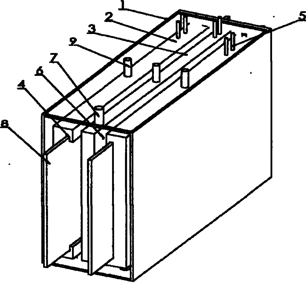
图中:1.壳体 2.阴极板 3.阳极板 4.沟槽 5.内加热电极6.小孔 7.输气管 8.半导体薄膜基板 9.极柱In the figure: 1. Shell 2.
图4为铜铟镓的硒化温度、时间和通混合气体时的工艺曲线。Fig. 4 is the process curve of copper indium gallium selenization temperature, time and when mixed gas is passed.
具体实施方式 Detailed ways
下面根据附图对本发明实施细节。The implementation details of the present invention will be described below according to the accompanying drawings.
一种等离子体辅助硒硫化处理装置,设置于真空室内,包括壳体1、阴极板2和阳极板3,壳体1为长方体结构,设有两块侧板和底板,阴极板2和阳极板3在壳体1内平行间隔交替叠放并固定在壳体1的底板上,阴极板2和阳极板3交替叠放形成等离子体发生器,壳体1的侧板即为等离子体发生器的外壳,阴极板2设有固定半导体薄膜基板8的沟槽4,阴极板2上设有均匀分布1~4个独立内加热电极5和电池基片测温点,阳极板3为腔体结构,阳极板3表面均布小孔6,孔径0.5mm~1.5mm,孔间距5mm~20mm,阳极板3上设有输气管7与腔体相通,阳极板3上设有均匀分布1~3个独立内加热电极5和阳极测温点,阴极板2和阳极板3分别设有极柱9并与真空室外的等离子体发生电源连接,所述内加热电极5、测温点和输气管7分别与真空室外的加热电源、电路及气路连接,内加热电极与测温点通过自动控温系统PID形成闭环温度控制,气路上设有气体流量计。A plasma-assisted selenium vulcanization treatment device is arranged in a vacuum chamber and includes a housing 1, a cathode plate 2 and an
实施例1Cu-In金属预制层的硒硫化处理Selenium vulcanization treatment of embodiment 1 Cu-In metal prefabricated layer
在普通钠钙玻璃上溅射沉积0.6~1.4μm厚金属Mo,用激光划线,再在Mo薄膜上溅射或蒸发一层NaF(厚0.1~0.3μm)(或Na2S),然后溅射沉积铜铟或铜铟合金,铜与铟的原子比(Cu/In)为0.85∶1.0~0.95∶1.0,将它们放入电容耦合平行板射频等离子体装置内阴极上基片架4上,关闭真空室抽真空。当机械泵与分子泵或真空扩散泵联动抽真空达到10-2~10-5Pa时,启动阴极板及阳极板内加热装置,其中阴极板的温度变化如图4所示。即让电池基板8以0.5~2℃/s的速度均匀地升温,并在100℃左右稳定10~20分钟后,关闭真空闸板阀到微启状态,降低真空室抽气速率,充入氩气,使真空室气压维持0.2~4Pa时,启动真空室外的等离子电源,使两平行电极的区域产生等离子体,然后再快速加热两平板电极,当阳极板3一侧温度达到180℃以上时,在先前通入氩气气路中通入固态硒蒸气、硫蒸气和氢气混合气体。同时阴极也快速升温到350℃并保温2~10min,再升温到550~600℃。这样,阳极表面均匀喷出的混合气体直接进入辉光等离子区,在射频电场和等离子体作用下,固态硒大分子团被分解、离化成活性硒原子或离子,氢分子被分解成氢原子或离子,随着反应的继续进行,在放置电池基片的平板电极端两侧面活性硒原子和氢原子与金属预制层进行硒化反应,在其相对平板电极内置气路端两侧的钼电极表面进行硒化氢合成反应,随着硒化氢浓度增加,逐渐向另一侧平板电极的电池基板表面扩散,渗入预制层内并被分解成活性硒原子和氢原子,直接参与金属预制层的硒化反应。当通入混合气体的阳极板温度超过280℃时,切断加热电源,控制其温度在160~350℃区间,阴极板(即基片)的温度在硒化处理过程中始终维持在350~600℃,其最佳温度区间是450~580℃。阴极板的温度变化曲线如图4所示。Sputter and deposit 0.6-1.4μm thick metal Mo on ordinary soda-lime glass, use laser scribing, then sputter or evaporate a layer of NaF (0.1-0.3μm thick) (or Na 2 S) on the Mo film, and then sputter Spray deposition of copper indium or copper indium alloy, the atomic ratio of copper to indium (Cu/In) is 0.85: 1.0 ~ 0.95: 1.0, put them into the substrate frame 4 on the cathode in the capacitively coupled parallel plate radio frequency plasma device, Close the vacuum chamber to evacuate. When the mechanical pump is linked with the molecular pump or the vacuum diffusion pump to achieve a vacuum of 10 -2 ~ 10 -5 Pa, start the heating device inside the cathode plate and the anode plate, and the temperature change of the cathode plate is shown in Figure 4. That is, let the battery substrate 8 evenly heat up at a rate of 0.5-2°C/s, and after stabilizing at about 100°C for 10-20 minutes, close the vacuum gate valve to a slightly open state, reduce the pumping rate of the vacuum chamber, and fill it with argon When the air pressure in the vacuum chamber is maintained at 0.2-4Pa, start the plasma power supply outside the vacuum chamber to generate plasma in the area of the two parallel electrodes, and then rapidly heat the two flat electrodes. When the temperature on one side of the
等离子体硒化处理10~50min后,切断变频电源,停止等离子体轰击半导体薄膜材料,将电池基板温度升高到580℃,保持20~30分钟,使多晶半导体材料小晶粒合并、长成大晶粒,减少半导体薄膜材料内部的缺陷态,此过程要继续向真空室内通入硒气氛和氢混合气体;然后,逐渐降低电池基板的温度,达到280℃时,切断硒蒸气、氢气和氩气,使射频等离子体辅助硒化或硫化装置自然降温,达到100℃时,向真空室充氩气快速降温,取出金属预制层已硒化转变成CuIn(Se,S)2化合物半导体薄膜材料的电池基板。After plasma selenization treatment for 10 to 50 minutes, cut off the variable frequency power supply, stop the plasma bombardment of semiconductor thin film materials, raise the temperature of the battery substrate to 580°C, and keep it for 20 to 30 minutes, so that the small grains of polycrystalline semiconductor materials can merge and grow into Large grains reduce the defect state inside the semiconductor thin film material. In this process, the selenium atmosphere and hydrogen mixed gas must be continuously introduced into the vacuum chamber; then, the temperature of the battery substrate is gradually reduced, and when it reaches 280°C, the selenium vapor, hydrogen and argon are cut off. Gas, so that the RF plasma-assisted selenization or vulcanization device naturally cools down. When it reaches 100 ° C, fill the vacuum chamber with argon gas to cool down quickly, and take out the metal prefabricated layer that has been selenized and transformed into CuIn(Se, S) 2 compound semiconductor thin film material. battery substrate.
将已硒化转变成CuInSe2半导体薄膜材料的电池基板放入化学水浴中,进行CBD-CdS缓冲层薄膜材料的沉积,其厚度大约50nm,用机械划线法在钼底电极线边的50~200nm处分割电池,吹净浮灰后放入真空室中溅射沉积高阻本征i-ZnO,其厚度60~80nm,方块电阻Rs=106~7欧姆/□,再溅射沉积低阻ZnO:Al,其厚度0.08~0.13μm,方块电阻Rs=10-3~4欧姆/□,再次进行机械划线分割电池,清理电池集成组件两侧Mo电极上的沉积物,真空蒸镀组件Ni/Al边电极导电带,集成组件全表面溅射MgF2减反射膜材料,厚0.1~0.12μm,焊接集成电池组件的电极引线,清理集成组件四周,用EVA树脂和低铁太阳能玻璃进行电池封装,就完成了CIS薄膜电池集成组件的生产。Put the battery substrate that has been selenized into CuInSe 2 semiconductor thin film material into a chemical water bath, and deposit the CBD-CdS buffer layer thin film material with a thickness of about 50nm. Divide the battery at 200nm, blow off the floating ash and put it in a vacuum chamber to sputter deposit high-resistance intrinsic i-ZnO with a thickness of 60-80nm and a sheet resistance Rs=10 6-7 ohm/□, then sputter-deposit low-resistance ZnO:Al, its thickness is 0.08~0.13μm, the square resistance Rs=10 -3~4 ohm/□, divide the battery by mechanical scribing again, clean the deposits on the Mo electrodes on both sides of the battery integrated component, and vacuum evaporate the component Ni / Al side electrode conductive belt, sputtering MgF 2 anti-reflection film material on the entire surface of the integrated module, with a thickness of 0.1-0.12 μm, welding the electrode leads of the integrated battery module, cleaning the surrounding of the integrated module, and packaging the battery with EVA resin and low-iron solar glass , completed the production of CIS thin film battery integrated components.
实施例2 CuIn0.3Ga0.7金属预制层的硒化处理Example 2 Selenization treatment of CuIn 0.3 Ga 0.7 metal prefabricated layer
电池基板表面电极的前期制备工艺与实施例1相同,在Mo薄膜表面先溅射或蒸发一层NaF(厚0.1~0.3μm)(或Na2S),再溅射沉积铜镓合金(CuGa0.3,厚度0.8~1.2μm),溅射沉积铟(0.5~0.8μm),或铜镓铟分别叠层沉积,其总化学配比应满足Cu(Ga0.3In0.7)Se2,并要求Cu/(In+Ga)=1∶1.0~1∶1.15,这是因为铟镓在硒化过程有一定升化损失,而钠离子的掺入有利于降低铜铟镓金属预制层硒化过程的结晶温度、晶粒长大和薄膜表面的平整度,提高CIGS薄膜电池吸收体的载流子浓度,在保持薄膜电池吸收体的电性能相近情况下,扩大了三元化合物半导体薄膜的成份有效范围,改善了薄膜电池的综合性能。The pre-preparation process of the electrode on the surface of the battery substrate is the same as in Example 1. A layer of NaF (0.1-0.3 μm thick) (or Na 2 S) is first sputtered or evaporated on the surface of the Mo film, and then a copper-gallium alloy (CuGa 0.3 , thickness 0.8~1.2μm), sputtering deposited indium (0.5~0.8μm), or copper-gallium-indium layered deposition respectively, the total chemical ratio should satisfy Cu(Ga 0.3 In 0.7 )Se 2 , and Cu/( In+Ga)=1:1.0~1:1.15, this is because indium gallium has a certain transformation loss in the selenization process, and the doping of sodium ions is beneficial to reduce the crystallization temperature of the copper indium gallium metal prefabricated layer selenization process, Grain growth and the flatness of the film surface increase the carrier concentration of the CIGS thin film battery absorber. While maintaining the similar electrical properties of the thin film battery absorber, the effective range of the composition of the ternary compound semiconductor film is expanded and the thin film is improved. Overall performance of the battery.
将预制好铜铟镓金属预制层放入平板变频等离子辅助硒化装置内,关闭真空室抽真空。当机械泵与分子泵或真空扩散泵联动抽真空达到10-2~10-5Pa时,启动阴极板及阳极板内加热装置,其中阴极板的温度变化如图4所示,即让电池基板以0.5~2℃/s的速度均匀地升温,并在100℃左右稳定10~20分钟后,关闭真空闸板阀到微启状态,降低真空室抽气速率,充入氩气,使真空室气压维持0.2~4Pa时,启动真空室外的等离子电源,使两平行电极的区域产生等离子体,然后再快速加热两平板电极,当阳极板3一侧温度达到180℃以上时,在先前通入氩气气路中通入固态硒蒸气和氢气混合气体。同时阴极也快速升温到350℃并保温2~10min,再升温到550~600℃。Put the prefabricated copper indium gallium metal prefabricated layer into the flat frequency conversion plasma assisted selenization device, and close the vacuum chamber to evacuate. When the mechanical pump is linked with the molecular pump or the vacuum diffusion pump to achieve a vacuum of 10 -2 ~ 10 -5 Pa, start the heating device in the cathode plate and the anode plate, and the temperature change of the cathode plate is shown in Figure 4, that is, let the battery substrate Raise the temperature uniformly at a rate of 0.5-2°C/s, and after stabilizing at about 100°C for 10-20 minutes, close the vacuum gate valve to the slightly open state, reduce the pumping rate of the vacuum chamber, and fill the vacuum chamber with argon to make the vacuum chamber When the air pressure is maintained at 0.2-4Pa, start the plasma power supply outside the vacuum chamber to generate plasma in the area of the two parallel electrodes, and then quickly heat the two flat electrodes. A mixed gas of solid selenium vapor and hydrogen is introduced into the gas path. At the same time, the temperature of the cathode is also rapidly raised to 350°C and kept for 2-10 minutes, and then the temperature is raised to 550-600°C.
因为硒化过程中CuSe2较其它硒化物的熔点低,Mo膜上先沉积铜镓合金层有利于CuSe2与Mo电极界面的浸润、优先与周围较难反应的镓生成更宽带隙的CuGaSe2,再逐渐与上表层的In相互扩散,最终生成Cu(In0.7Ga0.3)Se2化合物半导体薄膜,使薄膜电池吸收体在厚度纵深方向的带隙宽度发生渐变,并与Mo形成金属半导体结-薄膜电池背电场,提高电池的开路电压Voc;从另一方面来讲,在变频等离子体与电场作用下,固态硒大分子团被分解、离化成活性硒原子或离子,氢分子被分解成氢原子或离子,它们与预制层金属进行硒化反应,另一变频平板电极钼表面催化生成硒化氢,并逐渐扩散到预制层表面或内部,并被Mo电极所吸附、反应生成MoSe2,改善金属预制层硒化后与Mo电极的结合力。Because CuSe 2 has a lower melting point than other selenides in the selenization process, depositing a copper-gallium alloy layer on the Mo film first is conducive to the infiltration of CuSe 2 and the Mo electrode interface, and preferentially forms CuGaSe 2 with a wider band gap with the surrounding gallium that is difficult to react. , and then gradually interdiffused with In on the upper surface layer, finally forming a Cu(In 0.7 Ga 0.3 )Se 2 compound semiconductor film, which gradually changes the bandgap width of the thin film battery absorber in the thickness and depth direction, and forms a metal-semiconductor junction with Mo- The back electric field of the thin film battery increases the open circuit voltage Voc of the battery; on the other hand, under the action of the variable frequency plasma and the electric field, the solid selenium macromolecules are decomposed and ionized into active selenium atoms or ions, and the hydrogen molecules are decomposed into hydrogen Atoms or ions, they react with the metal of the prefabricated layer, and the molybdenum surface of the other variable frequency flat electrode catalyzes to generate hydrogen selenide, which gradually diffuses to the surface or inside of the prefabricated layer, and is adsorbed by the Mo electrode, reacts to generate MoSe 2 , and improves The bonding force between the metal prefabricated layer and the Mo electrode after selenization.
取出硒化好的铜铟镓硒多晶薄膜的电池基板,分别沉积CdS、i-ZnO、ZnO:Al和MgF等就制备出CIGS薄膜太阳电池组件,单体电池开路电压达500~740mV。Take out the cell substrate of selenized copper indium gallium selenide polycrystalline thin film, deposit CdS, i-ZnO, ZnO:Al and MgF respectively to prepare CIGS thin film solar cell module, and the open circuit voltage of the single cell reaches 500-740mV.
实施例3CIGS进行硒硫化Embodiment 3CIGS carries out selenium vulcanization
金属预置层CuInGa硒化后形成的CIGS半导体薄膜,如果再进行硫化,可以生成宽带隙、高阻、n型同质pn结,具有改进CIS及CIGS薄膜质量的作用。本实施例按照实施例2的方法在等离子辅助硒化制备CIGS薄膜材料的后期,将气体的成份改为输入Ar+H2S或Ar+S+H2后,可以在CIGS薄膜材料表层制备出含硫的高阻Cu(In0.7Ga0.3)(SeS)层,用EDX(能量分散型X射线分析仪)测试含硫薄膜表层的深度,确定控制其厚度在10~20nm时的通硫时间(3~10min);这种含硫表层薄膜构成了比底层CIGS薄膜的禁带宽度更宽的n型半导体层或CIGS的高阻层,该表层电阻率104Ω·cm以上,构成CIGS薄膜材料自身的同质pn结,制作成CIS或CIGS太阳能薄膜电池后,该工艺措施能抑制薄膜电池pn结界面缺陷产生的漏电流,提高该结区的二极管特性,达到降低漏电流增加电池开放端电压、提高电池填充因子FF和光电转换效率的目的。The CIGS semiconductor thin film formed after selenization of CuInGa metal pre-set layer, if vulcanized, can form wide bandgap, high resistance, n-type homogeneous pn junction, which can improve the quality of CIS and CIGS thin film. In this example, according to the method of Example 2, in the later stage of preparing CIGS thin film material by plasma-assisted selenization, after changing the composition of the gas into Ar+H 2 S or Ar+S+H 2 , it can be prepared on the surface layer of CIGS thin film material For the sulfur-containing high-resistance Cu(In 0.7 Ga 0.3 )(SeS) layer, use EDX (energy dispersive X-ray analyzer) to test the depth of the surface layer of the sulfur-containing film, and determine the sulfur-passing time when the thickness is controlled at 10-20nm ( 3~10min); this sulfur-containing surface layer film constitutes an n-type semiconductor layer or a CIGS high-resistance layer with a wider bandgap width than the underlying CIGS film, and the resistivity of the surface layer is above 10 4 Ω·cm, which constitutes a CIGS film material After its own homogeneous pn junction is made into a CIS or CIGS solar thin film battery, this process measure can suppress the leakage current caused by the pn junction interface defect of the thin film battery, improve the diode characteristics of the junction area, reduce the leakage current and increase the open terminal voltage of the battery , The purpose of improving the battery fill factor FF and photoelectric conversion efficiency.
这种表层含硫CIGS薄膜材料进行CBD-CdS沉积后,相对与表层不含硫的CIGS薄膜上沉积CdS后的相比,其界面晶格匹配效果更好,pn结界面区缺陷态更少。After the surface sulfur-containing CIGS thin film material is deposited with CBD-CdS, its interface lattice matching effect is better than that of the surface layer without sulfur after depositing CdS on the CIGS thin film, and there are fewer defect states in the pn junction interface region.
Claims (10)
Priority Applications (1)
| Application Number | Priority Date | Filing Date | Title |
|---|---|---|---|
| CN201010518539A CN102051603B (en) | 2010-10-26 | 2010-10-26 | Plasm-aided selenium sulfuration treatment device and process |
Applications Claiming Priority (1)
| Application Number | Priority Date | Filing Date | Title |
|---|---|---|---|
| CN201010518539A CN102051603B (en) | 2010-10-26 | 2010-10-26 | Plasm-aided selenium sulfuration treatment device and process |
Publications (2)
| Publication Number | Publication Date |
|---|---|
| CN102051603A CN102051603A (en) | 2011-05-11 |
| CN102051603B true CN102051603B (en) | 2012-10-24 |
Family
ID=43956391
Family Applications (1)
| Application Number | Title | Priority Date | Filing Date |
|---|---|---|---|
| CN201010518539A Expired - Fee Related CN102051603B (en) | 2010-10-26 | 2010-10-26 | Plasm-aided selenium sulfuration treatment device and process |
Country Status (1)
| Country | Link |
|---|---|
| CN (1) | CN102051603B (en) |
Families Citing this family (10)
| Publication number | Priority date | Publication date | Assignee | Title |
|---|---|---|---|---|
| CN102443779B (en) * | 2011-12-08 | 2014-06-25 | 尚越光电科技有限公司 | Plasma assisted selenylation technology and device for preparing copper-indium-gallium-selenium film |
| CN102738299A (en) * | 2012-06-06 | 2012-10-17 | 华东师范大学 | Method for producing copper, indium, gallium and selenium thin-film solar cell absorbing layer |
| CN102853940B (en) * | 2012-09-07 | 2013-12-18 | 顺德工业(江苏)有限公司 | High-temperature tester for lead frame |
| CN102909871B (en) * | 2012-09-29 | 2015-05-20 | 深圳南玻显示器件科技有限公司 | Surface processing device and processing method of flexible base material |
| CN103904154B (en) * | 2012-12-27 | 2016-06-29 | 北京有色金属研究总院 | A kind of modified model large scale sample selenization device |
| CN103074583B (en) * | 2013-01-25 | 2015-04-22 | 合肥工业大学 | Laser deposition preparation technology of CIGS film cell |
| CN103397305B (en) * | 2013-08-06 | 2015-08-26 | 深圳先进技术研究院 | Selenizing/sulfidizing device |
| TWI536585B (en) * | 2014-03-06 | 2016-06-01 | Ching Feng Chen | Thin film solar cells in the absorption layer of the production method and thin production method of membrane solar cell |
| CN104278251A (en) * | 2014-09-16 | 2015-01-14 | 阳江市汉能工业有限公司 | Metal preform layer alloying apparatus and method |
| CN107541718B (en) * | 2017-09-01 | 2020-01-21 | 苏州云舒新材料科技有限公司 | Preparation method of hydrotalcite-based magneto-optical film material |
Citations (3)
| Publication number | Priority date | Publication date | Assignee | Title |
|---|---|---|---|---|
| CN1379453A (en) * | 2001-04-12 | 2002-11-13 | 中国科学院长春光学精密机械与物理研究所 | Method suitable for growing zinc sulfide (selenide)-manganese film of broad-band semiconductor |
| CN101284654A (en) * | 2008-05-09 | 2008-10-15 | 南开大学 | A production method, device and application of a highly active selenium source for selenization treatment |
| CN201268719Y (en) * | 2008-10-07 | 2009-07-08 | 苏州富能技术有限公司 | Coating equipment for copper-indium-gallium-selenium-sulfur, copper-indium-gallium-selenium or copper-indium-gallium-sulfur film solar cell absorption layer |
Family Cites Families (1)
| Publication number | Priority date | Publication date | Assignee | Title |
|---|---|---|---|---|
| JP5246839B2 (en) * | 2006-08-24 | 2013-07-24 | 独立行政法人産業技術総合研究所 | Semiconductor thin film manufacturing method, semiconductor thin film manufacturing apparatus, photoelectric conversion element manufacturing method, and photoelectric conversion element |
-
2010
- 2010-10-26 CN CN201010518539A patent/CN102051603B/en not_active Expired - Fee Related
Patent Citations (3)
| Publication number | Priority date | Publication date | Assignee | Title |
|---|---|---|---|---|
| CN1379453A (en) * | 2001-04-12 | 2002-11-13 | 中国科学院长春光学精密机械与物理研究所 | Method suitable for growing zinc sulfide (selenide)-manganese film of broad-band semiconductor |
| CN101284654A (en) * | 2008-05-09 | 2008-10-15 | 南开大学 | A production method, device and application of a highly active selenium source for selenization treatment |
| CN201268719Y (en) * | 2008-10-07 | 2009-07-08 | 苏州富能技术有限公司 | Coating equipment for copper-indium-gallium-selenium-sulfur, copper-indium-gallium-selenium or copper-indium-gallium-sulfur film solar cell absorption layer |
Also Published As
| Publication number | Publication date |
|---|---|
| CN102051603A (en) | 2011-05-11 |
Similar Documents
| Publication | Publication Date | Title |
|---|---|---|
| CN102051603B (en) | Plasm-aided selenium sulfuration treatment device and process | |
| JP5246839B2 (en) | Semiconductor thin film manufacturing method, semiconductor thin film manufacturing apparatus, photoelectric conversion element manufacturing method, and photoelectric conversion element | |
| CN102054897B (en) | Method for preparing thin film solar cell from multi-element alloy single target material | |
| CN101814553B (en) | Photo-assisted preparation of light-absorbing layer of copper indium gallium selenide thin film solar cells | |
| CN102751388B (en) | A kind of preparation method of copper indium gallium selenide thin film solar cell | |
| CN102354711B (en) | Copper indium gallium selenide thin film solar cell module and preparation method of light absorption layer thereof | |
| US9559247B2 (en) | Photovoltaic device containing an N-type dopant source | |
| TWI589011B (en) | Compound solar cell and method of manufacturing same | |
| KR101067295B1 (en) | Thin film solar cell and manufacturing method thereof | |
| US10211351B2 (en) | Photovoltaic cell with high efficiency CIGS absorber layer with low minority carrier lifetime and method of making thereof | |
| WO2013185506A1 (en) | Method for preparing copper indium gallium diselenide thin-film solar cell | |
| US20160005893A1 (en) | Cigs type compound solar cell | |
| CN101777604A (en) | Method for preparing thin film solar cell adsorbing layer CuInSe2 film | |
| JP2010192690A (en) | Method of manufacturing solar cell | |
| KR101734362B1 (en) | Forming method for acigs film at low temperature and manufacturing method for solar cell by using the forming method | |
| US8258003B2 (en) | Manufacturing method of compound semiconductor solar cell | |
| Elhady et al. | A review of thin film solar cells | |
| CN101414650B (en) | A kind of preparation method of nanocrystalline/amorphous silicon two-phase thin film solar cell | |
| CN110752266A (en) | Buffer layer of copper indium gallium selenide thin film solar cell chip and preparation method thereof, and copper indium gallium selenide thin film solar cell chip | |
| CN102723399B (en) | A Chemical Preparation Process of Cu(InAl)Se2 Thin Film | |
| JP5770294B2 (en) | Photoelectric conversion device and manufacturing method thereof | |
| CN105932093B (en) | A kind of preparation method of high quality CIGS thin film solar battery obsorbing layer | |
| KR101444188B1 (en) | Apparatus for making the photovoltaic absorber layer | |
| CN102157595A (en) | Silicon film/Cu(In, Ga)Se2 binode film battery process | |
| JP6861480B2 (en) | Manufacturing method of photoelectric conversion module |
Legal Events
| Date | Code | Title | Description |
|---|---|---|---|
| C06 | Publication | ||
| PB01 | Publication | ||
| C10 | Entry into substantive examination | ||
| SE01 | Entry into force of request for substantive examination | ||
| C14 | Grant of patent or utility model | ||
| GR01 | Patent grant | ||
| CF01 | Termination of patent right due to non-payment of annual fee |
Granted publication date: 20121024 Termination date: 20161026 |
|
| CF01 | Termination of patent right due to non-payment of annual fee |