CN101997015B - Solid-state imaging device, method for manufacturing sol-state imaging device and electronic apparatus - Google Patents
Solid-state imaging device, method for manufacturing sol-state imaging device and electronic apparatus Download PDFInfo
- Publication number
- CN101997015B CN101997015B CN201010250753.XA CN201010250753A CN101997015B CN 101997015 B CN101997015 B CN 101997015B CN 201010250753 A CN201010250753 A CN 201010250753A CN 101997015 B CN101997015 B CN 101997015B
- Authority
- CN
- China
- Prior art keywords
- area
- gate electrode
- signal
- transistor
- region
- Prior art date
- Legal status (The legal status is an assumption and is not a legal conclusion. Google has not performed a legal analysis and makes no representation as to the accuracy of the status listed.)
- Expired - Fee Related
Links
Images


Classifications
-
- H—ELECTRICITY
- H10—SEMICONDUCTOR DEVICES; ELECTRIC SOLID-STATE DEVICES NOT OTHERWISE PROVIDED FOR
- H10F—INORGANIC SEMICONDUCTOR DEVICES SENSITIVE TO INFRARED RADIATION, LIGHT, ELECTROMAGNETIC RADIATION OF SHORTER WAVELENGTH OR CORPUSCULAR RADIATION
- H10F39/00—Integrated devices, or assemblies of multiple devices, comprising at least one element covered by group H10F30/00, e.g. radiation detectors comprising photodiode arrays
- H10F39/80—Constructional details of image sensors
- H10F39/803—Pixels having integrated switching, control, storage or amplification elements
-
- H—ELECTRICITY
- H10—SEMICONDUCTOR DEVICES; ELECTRIC SOLID-STATE DEVICES NOT OTHERWISE PROVIDED FOR
- H10F—INORGANIC SEMICONDUCTOR DEVICES SENSITIVE TO INFRARED RADIATION, LIGHT, ELECTROMAGNETIC RADIATION OF SHORTER WAVELENGTH OR CORPUSCULAR RADIATION
- H10F39/00—Integrated devices, or assemblies of multiple devices, comprising at least one element covered by group H10F30/00, e.g. radiation detectors comprising photodiode arrays
- H10F39/011—Manufacture or treatment of image sensors covered by group H10F39/12
- H10F39/014—Manufacture or treatment of image sensors covered by group H10F39/12 of CMOS image sensors
-
- H—ELECTRICITY
- H10—SEMICONDUCTOR DEVICES; ELECTRIC SOLID-STATE DEVICES NOT OTHERWISE PROVIDED FOR
- H10F—INORGANIC SEMICONDUCTOR DEVICES SENSITIVE TO INFRARED RADIATION, LIGHT, ELECTROMAGNETIC RADIATION OF SHORTER WAVELENGTH OR CORPUSCULAR RADIATION
- H10F39/00—Integrated devices, or assemblies of multiple devices, comprising at least one element covered by group H10F30/00, e.g. radiation detectors comprising photodiode arrays
- H10F39/011—Manufacture or treatment of image sensors covered by group H10F39/12
- H10F39/016—Manufacture or treatment of image sensors covered by group H10F39/12 of thin-film-based image sensors
-
- H—ELECTRICITY
- H10—SEMICONDUCTOR DEVICES; ELECTRIC SOLID-STATE DEVICES NOT OTHERWISE PROVIDED FOR
- H10F—INORGANIC SEMICONDUCTOR DEVICES SENSITIVE TO INFRARED RADIATION, LIGHT, ELECTROMAGNETIC RADIATION OF SHORTER WAVELENGTH OR CORPUSCULAR RADIATION
- H10F39/00—Integrated devices, or assemblies of multiple devices, comprising at least one element covered by group H10F30/00, e.g. radiation detectors comprising photodiode arrays
- H10F39/80—Constructional details of image sensors
- H10F39/803—Pixels having integrated switching, control, storage or amplification elements
- H10F39/8037—Pixels having integrated switching, control, storage or amplification elements the integrated elements comprising a transistor
-
- H—ELECTRICITY
- H10—SEMICONDUCTOR DEVICES; ELECTRIC SOLID-STATE DEVICES NOT OTHERWISE PROVIDED FOR
- H10F—INORGANIC SEMICONDUCTOR DEVICES SENSITIVE TO INFRARED RADIATION, LIGHT, ELECTROMAGNETIC RADIATION OF SHORTER WAVELENGTH OR CORPUSCULAR RADIATION
- H10F39/00—Integrated devices, or assemblies of multiple devices, comprising at least one element covered by group H10F30/00, e.g. radiation detectors comprising photodiode arrays
- H10F39/80—Constructional details of image sensors
- H10F39/813—Electronic components shared by multiple pixels, e.g. one amplifier shared by two pixels
Landscapes
- Solid State Image Pick-Up Elements (AREA)
Abstract
涉及固体摄像器件及其制造方法和电子装置,该固体摄像器件包括:光电转换单元,它包括第一导电型的第一区域和第二导电型的第二区域,第一区域与第二区域之间形成pn结,第一区域和第二区域形成在半导体基板的信号读出面中,第二区域位于比第一区域深的位置处;以及传输晶体管,它形成在信号读出面中,并且被构造为通过沟道区域将累积在光电转换单元中的信号电荷传输到读出漏极,沟道区域位于第一区域的表面下方且在水平方向上与光电转换单元相邻。传输晶体管包括以延伸越过台阶的方式从沟道区域上方延伸至第一区域上方的传输栅极电极传输栅极电极与沟道区域之间隔着栅极绝缘膜。因此,能实现高饱和信号电平、高灵敏度和低随机噪声。

It relates to a solid-state imaging device, a manufacturing method thereof, and an electronic device. The solid-state imaging device includes: a photoelectric conversion unit, which includes a first region of the first conductivity type and a second region of the second conductivity type. A pn junction is formed between the first region and the second region formed in the signal readout surface of the semiconductor substrate, the second region being located at a position deeper than the first region; and a transfer transistor formed in the signal readout surface, and The signal charge accumulated in the photoelectric conversion unit is transferred to the readout drain through a channel region located below the surface of the first region and adjacent to the photoelectric conversion unit in the horizontal direction. The transfer transistor includes a transfer gate electrode extending from above the channel region to above the first region in a manner extending over a step, with a gate insulating film interposed between the transfer gate electrode and the channel region. Therefore, a high saturation signal level, high sensitivity, and low random noise can be realized.
Description
相关申请的交叉参考 Cross References to Related Applications
本申请包含与2009年8月20日向日本专利局提交的日本在先专利申请JP 2009-191133的公开内容相关的主题,将该在先申请的全部内容以引用的方式并入本文。 This application contains subject matter related to the disclosure of Japanese Priority Patent Application JP 2009-191133 filed in Japan Patent Office on Aug. 20, 2009, the entire content of which is hereby incorporated by reference. the
技术领域 technical field
本发明涉及固体摄像器件、电子装置和固体摄像器件的制造方法。 The present invention relates to a solid-state imaging device, an electronic device, and a method for manufacturing the solid-state imaging device. the
背景技术 Background technique
例如数码摄像机和数码相机等电子装置包括固体摄像器件。在电子装置中所包括的固体摄像器件的示例包括互补金属氧化物半导体(complementary metal oxide semiconductor,CMOS)型图像传感器和电荷耦合器件(charge coupled device,CCD)型图像传感器。 Electronic devices such as digital video cameras and digital still cameras include solid-state imaging devices. Examples of solid-state imaging devices included in electronic devices include complementary metal oxide semiconductor (CMOS) type image sensors and charge coupled device (CCD) type image sensors. the
固体摄像器件具有在半导体基板表面上的摄像区域。该摄像区域为形成有多个像素的区域。在该摄像区域中还形成有与像素对应的多个光电转换元件。光电转换元件接收来自所要拍摄的物体的光,并且将光转换成电荷以产生信号电荷。例如,光电二极管形成为这种光电转换元件。每个光电二极管在其pn结处通过将所接收到的光转换成电荷来产生信号电荷,并且累积这些信号电荷。 A solid-state imaging device has an imaging region on the surface of a semiconductor substrate. This imaging area is an area where a plurality of pixels are formed. A plurality of photoelectric conversion elements corresponding to pixels are also formed in the imaging region. The photoelectric conversion element receives light from an object to be photographed, and converts the light into charges to generate signal charges. For example, a photodiode is formed as such a photoelectric conversion element. Each photodiode generates signal charges at its pn junction by converting received light into charges, and accumulates the signal charges. the
固体摄像器件的一个示例为CMOS图像传感器。已经想到这样一种CMOS图像传感器:在绝缘体上硅(silicon-on-insulator,SOI)基板的除去了氧化硅的部分中形成有传输晶体管,并且在SOI基板的顶部硅层上形成有像素晶体管。对于该CMOS图像传感器而言,已经提出将光电二极管延伸到达像素晶体管下方的部分。这是因为当在采用了能够通过诸如减少暗电流、白点和残留图像等来改善特性的埋入式光电二极管的固体摄像器件中使用这种结构时,会减小固体摄像器件的尺寸,并且可以增加固体摄像器件的饱和电子数(例如,参见日本待审专利申请公开公报 No.2006-173351以及Xinyu Zheng,Suresh Seahadri,Michael Wood,ChrisWrigley,and Bedabrate Pain著“Process and Pixels for High PerformanceImager in SOI-CMOS Technology”(Germany),IEEE workshop oncharge-coupled Device & Advanced Image Sensors,2003年5月)。 One example of a solid-state imaging device is a CMOS image sensor. A CMOS image sensor has been conceived in which a transfer transistor is formed in a silicon-on-insulator (SOI) substrate from which silicon oxide is removed, and a pixel transistor is formed on a top silicon layer of the SOI substrate. For this CMOS image sensor, it has been proposed to extend the photodiode to the part below the pixel transistor. This is because when such a structure is used in a solid-state imaging device employing an embedded photodiode capable of improving characteristics such as reduction of dark current, white point, and residual image, the size of the solid-state imaging device is reduced, and The number of saturation electrons of solid-state imaging devices can be increased (for example, see Japanese Unexamined Patent Application Publication No. 2006-173351 and Xinyu Zheng, Suresh Seahadri, Michael Wood, Chris Wrigley, and Bedabrate Pain "Process and Pixels for High Performance Imager in SOI -CMOS Technology” (Germany), IEEE workshop oncharge-coupled Device & Advanced Image Sensors, May 2003). the
为了形成从保留了埋置氧化物(buried oxide,BOX)层的SOI基板的部分连续延伸至已经除去了BOX层的部分的光电二极管,最好在除去BOX层之前进行离子注入。这意味着在用于形成光电二极管的离子注入之后形成传输栅极电极。但是,这会造成在传输栅极电极和光电二极管之间出现较大的错位。 In order to form a photodiode extending continuously from a portion of the SOI substrate where a buried oxide (BOX) layer remains to a portion where the BOX layer has been removed, ion implantation is preferably performed before removing the BOX layer. This means that the transfer gate electrode is formed after the ion implantation used to form the photodiode. However, this causes a large misalignment between the transfer gate electrode and the photodiode. the
在光电二极管不在除了传输晶体管之外的像素晶体管下方延伸时,可以首先形成传输栅极电极,然后可以采用传输电极作为掩模以自对准方式注入离子。这可以消除在光电二极管和除了传输晶体管之外的像素晶体管之间的错位。 When the photodiode does not extend under the pixel transistor other than the transfer transistor, the transfer gate electrode can be formed first, and then ions can be implanted in a self-aligned manner using the transfer electrode as a mask. This can eliminate misalignment between photodiodes and pixel transistors other than transfer transistors. the
但是,难以采用该过程来形成在除了传输晶体管之外的像素晶体管下方延伸的光电二极管。因此,在传输晶体管和光电二极管之间仍然会出现错位。因此,将信号电荷从光电二极管传输到浮动扩散部的效率会降低,并且所拍摄的图像的质量会下降。 However, it is difficult to employ this process to form a photodiode extending under a pixel transistor other than a transfer transistor. Therefore, misalignment still occurs between the pass transistor and the photodiode. Therefore, the efficiency of transferring signal charges from the photodiode to the floating diffusion decreases, and the quality of captured images decreases. the
发明内容 Contents of the invention
期望提供能够改善所拍摄图像的图像质量的固体摄像器件和电子装置以及该固体摄像器件的制造方法。 It is desirable to provide a solid-state imaging device and an electronic device capable of improving the image quality of captured images, and a method of manufacturing the solid-state imaging device. the
本发明的实施例提供了一种固体摄像器件的制造方法,所述固体摄像器件包括具有信号读出面的半导体基板,在所述信号读出面中形成有光电转换单元和传输晶体管,所述光电转换单元包括第一区域和第二区域,所述第一区域与所述第二区域之间形成pn结,所述传输晶体管被构造为通过沟道区域将信号电荷从所述光电转换单元传输到读出漏极。所述制造方法包括以下步骤:通过将第一导电型的杂质离子注入到所述信号读出面的将要形成所述光电转换单元、所述沟道区域和所述读出漏极的部分中,在所述半导体基板中形成所述第一区域;通过将第二导电型的杂质注入到所述信号读出面的将要形成所述光电转换单元、所述沟道区域和所述读出漏极且比所述第一区域深的部分中,在所述半导体基板中形成所述第二区域;在所述信号读出面上形成抗蚀剂图形,所述抗蚀剂图形具有开口,所述开口使将要形成所述沟道区域和所述读出漏极的所述信号读出面的部分暴露出来;采用所述抗蚀剂图形作为掩模,通过将第一导电型的杂质注入到所述信号读出面的将要形成所述沟道区域和所述读出漏极且比所述第一区域深的部分中,在所述半导体基板中形成第三区域;通过蚀刻所述第一区域的除去位于所述第三区域上方的部分;在所述半导体基板的信号读出面的已经除去了所述第一区域的部分上形成所述传输晶体管的栅极绝缘膜;形成传输栅极电极,所述传输栅极电极从所述沟道区域上方延伸至所述第一区域上方,且所述传输栅极电极与所述沟道区域之间隔着所述栅极绝缘膜;以及采用所述传输栅极电极作为掩模,通过将第二导电型的杂质离子注入到所述半导体基板的信号读出面的已经除去了所述第一区域的部分中,形成所述读出漏极。 An embodiment of the present invention provides a method of manufacturing a solid-state imaging device including a semiconductor substrate having a signal readout surface in which a photoelectric conversion unit and a transfer transistor are formed. The photoelectric conversion unit includes a first region and a second region between which a pn junction is formed, and the transfer transistor is configured to transfer signal charges from the photoelectric conversion unit through a channel region to the read drain. The manufacturing method includes the following steps: by implanting impurity ions of the first conductivity type into the portion of the signal readout surface where the photoelectric conversion unit, the channel region and the readout drain are to be formed, The first region is formed in the semiconductor substrate; the photoelectric conversion unit, the channel region and the readout drain are to be formed by implanting impurities of a second conductivity type into the signal readout surface. and in a portion deeper than the first region, the second region is formed in the semiconductor substrate; a resist pattern is formed on the signal readout surface, the resist pattern has an opening, the The opening exposes the portion of the signal readout surface where the channel region and the readout drain will be formed; using the resist pattern as a mask, by implanting impurities of the first conductivity type into the In the portion of the signal readout surface where the channel region and the readout drain are to be formed and is deeper than the first region, a third region is formed in the semiconductor substrate; by etching the first region removing a portion above the third region; forming a gate insulating film of the transfer transistor on a portion of the signal readout surface of the semiconductor substrate from which the first region has been removed; forming a transfer gate electrode , the transfer gate electrode extends from above the channel region to above the first region, and the transfer gate electrode and the channel region are separated by the gate insulating film; and using the The transfer gate electrode serves as a mask, and the readout drain is formed by implanting impurity ions of the second conductivity type into a portion of the signal readout surface of the semiconductor substrate from which the first region has been removed.
在该实施例中,采用相同的掩模来形成第三区域并除去第一区域。因此,第三区域可以以自对准的方式形成。然后,传输栅极电极形成为从在已经除去了第一区域的部分中的沟道形成区域上方延伸至光电转换单元上方。传输栅极电极用作掩模,以自对准的方式形成读出漏极。因此,在传输栅极电极和光电转换单元之间以及在传输栅极电极和读出漏极之间不会出现错位。因此,能够抑制由错位引起的传输信号电荷的效率降低。 In this embodiment, the same mask is used to form the third region and remove the first region. Therefore, the third region can be formed in a self-aligned manner. Then, the transfer gate electrode is formed to extend from above the channel formation region in the portion from which the first region has been removed to above the photoelectric conversion unit. The transfer gate electrode is used as a mask to form the read drain in a self-aligned manner. Therefore, no misalignment occurs between the transfer gate electrode and the photoelectric conversion unit and between the transfer gate electrode and the readout drain. Therefore, it is possible to suppress reduction in efficiency of transferring signal charges caused by dislocation. the
本发明的另一个实施例提供了固体摄像器件,所述固体摄像器件包括:光电转换单元,它包括第一导电型的第一区域和第二导电型的第二区域,所述第一区域与所述第二区域之间形成pn结,所述第一区域和所述第二区域形成在所述半导体基板的信号读出面中,所述第二区域位于比所述第一区域深的位置处;以及传输晶体管,它形成在所述信号读出面中,并且被构造为通过沟道区域将累积在所述光电转换单元中的信号电荷传输到读出漏极,所述沟道区域位于所述第一区域的表面下方以在它们之间形成台阶,且所述沟道区域在水平方向上与所述光电转换单元相邻。所述传输晶体管包括传输栅极电极,且所述传输栅极电极以延伸越过所述台阶的方式从所述沟道区域上方延伸至所述第一区域上方,所述传输栅极电极与所述沟道区域之间隔着栅极绝缘膜。 Another embodiment of the present invention provides a solid-state imaging device including: a photoelectric conversion unit including a first region of a first conductivity type and a second region of a second conductivity type, the first region and A pn junction is formed between the second regions, the first region and the second region are formed in the signal readout surface of the semiconductor substrate, the second region is located deeper than the first region and a transfer transistor formed in the signal readout face and configured to transfer the signal charge accumulated in the photoelectric conversion unit to the readout drain through a channel region located at The surface of the first region is below to form a step therebetween, and the channel region is adjacent to the photoelectric conversion unit in the horizontal direction. The transfer transistor includes a transfer gate electrode extending from above the channel region to above the first region in a manner extending over the step, the transfer gate electrode being connected to the first region. A gate insulating film is interposed between the channel regions. the
根据该实施例,传输栅极电极和光电转换单元之间的位置关系由该台阶决定。因此,不存在错位的负面效应,并且改善了传输信号电荷的效率。 According to this embodiment, the positional relationship between the transfer gate electrode and the photoelectric conversion unit is determined by the steps. Therefore, there is no negative effect of dislocation, and the efficiency of transferring signal charges is improved. the
本发明的另一个实施例提供了固体摄像器件,所述固体摄像器件包括:光电转换单元,它包括形成在半导体基板的信号读出面中的第一导电型的第一区域和第二导电型的第二区域,所述半导体基板包括半导体层、在所述半导体层下方的绝缘膜和在所述绝缘膜下方的半导体区域,在所述半导体区域中所述第一区域与所述第二区域之间形成pn结,所述第二区域位于比所述第一区域深的位置处;以及传输晶体管,它设置在所述信号读出面中,并且被构造为通过沟道区域将累积在所述光电转换单元中的信号电荷传输到读出漏极。所述传输晶体管包括传输栅极电极,所述传输栅极电极延伸越过所述读出漏极侧的除去了所述绝缘膜的部分与所述光电转换单元侧的未除去所述绝缘膜的部分之间的台阶。 Another embodiment of the present invention provides a solid-state imaging device including: a photoelectric conversion unit including a first region of a first conductivity type and a second conductivity type region formed in a signal readout surface of a semiconductor substrate; The second region of the semiconductor substrate includes a semiconductor layer, an insulating film under the semiconductor layer, and a semiconductor region under the insulating film, and in the semiconductor region, the first region and the second region A pn junction is formed therebetween, the second region is located at a position deeper than the first region; and a transfer transistor is provided in the signal readout plane and is configured to pass through the channel region to accumulate in the The signal charge in the photoelectric conversion unit is transferred to the readout drain. The transfer transistor includes a transfer gate electrode extending across a portion of the readout drain side from which the insulating film is removed and a portion of the photoelectric conversion unit side from which the insulating film is not removed. between steps. the
本发明的再一个实施例提供了一种电子装置,所述电子装置包括:光电转换单元,它包括第一导电型的第一区域和第二导电型的第二区域,所述第一区域与所述第二区域之间形成pn结,所述第一区域和所述第二区域形成在所述半导体基板的信号读出面中,所述第二区域位于比所述第一区域深的位置处;以及传输晶体管,它形成在所述信号读出面中,并且被构造为通过沟道区域将累积在所述光电转换单元中的信号电荷传输到读出漏极,所述沟道区域位于所述第一区域的表面下方以在它们之间形成台阶,且所述沟道区域在水平方向上与所述光电转换单元相邻。所述传输栅极电极以延伸越过所述台阶的方式从所述沟道区域上方延伸至所述第一区域上方,且所述传输栅极电极与所述沟道区域之间隔着栅极绝缘膜。 Another embodiment of the present invention provides an electronic device, the electronic device includes: a photoelectric conversion unit, which includes a first region of the first conductivity type and a second region of the second conductivity type, the first region and A pn junction is formed between the second regions, the first region and the second region are formed in the signal readout surface of the semiconductor substrate, the second region is located deeper than the first region and a transfer transistor formed in the signal readout face and configured to transfer the signal charge accumulated in the photoelectric conversion unit to the readout drain through a channel region located at The surface of the first region is below to form a step therebetween, and the channel region is adjacent to the photoelectric conversion unit in the horizontal direction. The transfer gate electrode extends from above the channel region to above the first region in a manner extending over the step, and a gate insulating film is interposed between the transfer gate electrode and the channel region . the
根据本发明的这些实施例,可以提供能够改善所拍摄图像的图像质量的固体摄像器件和电子装置以及固体摄像器件的制造方法。 According to the embodiments of the present invention, it is possible to provide a solid-state imaging device and an electronic device capable of improving the image quality of a captured image, and a method of manufacturing the solid-state imaging device. the
附图说明Description of drawings
图1是示出了根据本发明实施例的照相机结构的图。 FIG. 1 is a diagram showing the structure of a camera according to an embodiment of the present invention. the
图2为根据本发明第一实施例的固体摄像器件的整体结构的示意性平面图。 2 is a schematic plan view of the overall structure of the solid-state imaging device according to the first embodiment of the present invention. the
图3为示出了第一实施例的摄像区域中的像素的相关部分的电路图。 FIG. 3 is a circuit diagram showing a relevant portion of a pixel in an imaging region of the first embodiment. the
图4为示出了根据第一实施例在从像素P中读取信号时供给到各个单元的脉冲信号的时序图。 FIG. 4 is a timing chart showing pulse signals supplied to respective units when reading a signal from a pixel P according to the first embodiment. the
图5为根据第一实施例的固体摄像器件的截面图。 Fig. 5 is a cross-sectional view of the solid-state imaging device according to the first embodiment. the
图6A~图9B为示出了在第一实施例的固体摄像器件的制造方法的各个步骤中的相关部分的截面图。 6A to 9B are cross-sectional views showing relevant parts in respective steps of the method of manufacturing the solid-state imaging device of the first embodiment. the
图10为根据第二实施例的固体摄像器件的截面图。 Fig. 10 is a cross-sectional view of a solid-state imaging device according to a second embodiment. the
图11A~图11C为示出了在第二实施例的固体摄像器件的制造方法的各个步骤中的相关部分的截面图。 11A to 11C are cross-sectional views showing relevant parts in respective steps of the method of manufacturing the solid-state imaging device of the second embodiment. the
图12为根据本发明第三实施例的固体摄像器件的截面图。 12 is a cross-sectional view of a solid-state imaging device according to a third embodiment of the present invention. the
图13A~图14B为示出了在第三实施例的固体摄像器件的制造方法的各个步骤中的相关部分的截面图。 13A to 14B are cross-sectional views showing relevant parts in respective steps of the method of manufacturing the solid-state imaging device of the third embodiment. the
图15为示出了根据本发明第四实施例的固体摄像器件的相关部分的示意图。 FIG. 15 is a schematic diagram showing relevant parts of a solid-state imaging device according to a fourth embodiment of the present invention. the
图16为根据第四实施例的固体摄像器件的截面图。 16 is a cross-sectional view of a solid-state imaging device according to a fourth embodiment. the
图17为示出了设在第四实施例的摄像区域中的像素P的相关部分的电路图。 FIG. 17 is a circuit diagram showing a relevant part of a pixel P provided in the imaging area of the fourth embodiment. the
图18A和图18B为示出了在第四实施例的固体摄像器件的制造方法的各个步骤中的相关部分的截面图。 18A and 18B are cross-sectional views showing relevant parts in respective steps of the method of manufacturing the solid-state imaging device of the fourth embodiment. the
图19为示出了固体摄像器件的变形的截面图。 FIG. 19 is a cross-sectional view showing a modification of the solid-state imaging device. the
具体实施方式 Detailed ways
现在将参照这些附图按照以下顺序对本发明的实施例进行说明。 Embodiments of the present invention will now be described in the following order with reference to these drawings. the
1.第一实施例(在BOX层上形成传输栅极电极) 1. First embodiment (formation of transfer gate electrode on BOX layer)
2.第二实施例(在基板(P+)上形成传输栅极电极) 2. Second Embodiment (Formation of Transfer Gate Electrode on Substrate (P + ))
3.第三实施例(在顶部硅层上形成传输栅极电极) 3. Third Embodiment (Formation of Transfer Gate Electrode on Top Silicon Layer)
4.第四实施例(在氧化物膜上形成传输栅极电极) 4. Fourth Embodiment (Formation of Transfer Gate Electrode on Oxide Film)
1.第一实施例1. The first embodiment
[A]器件结构 [A] Device structure
(1)照相机的整体结构 (1) The overall structure of the camera
图1为示出了根据本发明实施例的照相机的结构的图。 FIG. 1 is a diagram showing the structure of a camera according to an embodiment of the present invention. the
如图1所示,照相机200包括稍后将说明的固体摄像器件1、光学系统202、驱动电路203和信号处理电路204。
As shown in FIG. 1 , a camera 200 includes a solid-
固体摄像器件1具有接收通过光学系统202进入的入射光(所要拍摄物体的图像)的表面。固体摄像器件1将入射光转换成电荷,从而产生信号电荷并且输出原始数据。固体摄像器件1根据从驱动电路203输出的控制信号受到驱动。下面将说明该固体摄像器件1的详细结构。
The solid-
光学系统202包括摄像透镜(未图示)和光圈(未图示),并且被布置成将所拍摄物体的图像的入射光聚集在固体摄像器件1的表面PS上。
The optical system 202 includes an imaging lens (not shown) and a diaphragm (not shown), and is arranged to condense incident light of a captured image of an object on the surface PS of the solid-
更具体地说,如图1所示,光学系统202在固体摄像器件1的表面PS的中央部分中沿着与表面PS垂直的方向发射主光线L。但是,朝着表面PS的周边部分发射的主光线L相对于与表面PS垂直的方向倾斜。由于在光学系统202中出射光瞳距离是有限的,所以朝着固体摄像器件1的表面PS发射的主光线L随着距表面PS中心的距离的增大而逐渐倾斜。
More specifically, as shown in FIG. 1 , the optical system 202 emits a chief ray L in a direction perpendicular to the surface PS in the central portion of the surface PS of the solid-
驱动电路203向固体摄像器件1和信号处理电路204输出各种控制信号,并且控制固体摄像器件1和信号处理电路204的操作。
The drive circuit 203 outputs various control signals to the solid-
信号处理电路204被构成为通过对从固体摄像器件1输出的原始数据进行信号处理而产生所要拍摄物体的数字图像。
The signal processing circuit 204 is configured to generate a digital image of a subject to be photographed by performing signal processing on raw data output from the solid-
(2)固体摄像器件的整体结构 (2) The overall structure of the solid-state imaging device
下面对固体摄像器件1的整体结构进行说明。
Next, the overall structure of the solid-
图2为根据本发明第一实施例的固体摄像器件的整体结构的示意性平面图。 2 is a schematic plan view of the overall structure of the solid-state imaging device according to the first embodiment of the present invention. the
该实施例的固体摄像器件1为CMOS型图像传感器,并且包括如图2所示的半导体基板101。如图2所示,半导体基板101在表面中具有摄像区域PA和周边区域SA。半导体基板101例如由硅构成。
The solid-
(2-1)摄像区域 (2-1) Camera area
下面对摄像区域PA进行说明。 Next, the imaging area PA will be described. the
参照图2,摄像区域PA具有矩形形状,并且具有沿着x方向和y方向排列的像素P。换句话说,像素P以矩阵状布置。该摄像区域PA被布置为它的中心与在图1中所示的光学系统202的光轴对准。摄像区域PA相当于在图1中所示的表面PS。 Referring to FIG. 2 , the imaging area PA has a rectangular shape, and has pixels P arranged along the x-direction and the y-direction. In other words, the pixels P are arranged in a matrix. The imaging area PA is arranged such that its center is aligned with the optical axis of the optical system 202 shown in FIG. 1 . The imaging area PA corresponds to the surface PS shown in FIG. 1 . the
图3为示出了第一实施例的摄像区域中的像素的相关部分的电路图。 FIG. 3 is a circuit diagram showing a relevant portion of a pixel in an imaging region of the first embodiment. the
如图3所示,在摄像区域PA中形成的像素P包括光电二极管21、传输晶体管22、放大晶体管23、选择晶体管24和复位晶体管25。
As shown in FIG. 3 , the pixel P formed in the imaging area PA includes a
如图3所示,像素P的光电二极管21包括接地阳极和与传输晶体管22连接的阴极。
As shown in FIG. 3 , the
如图3所示,在像素P中,传输晶体管22设在光电二极管21和浮动扩散部FD之间。传输晶体管22的栅极电极连接至传输线26。当传输脉冲从传输线26被供给到栅极电极时,传输晶体管22把在光电二极管21中产生的信号电荷传输到浮动扩散部FD。
As shown in FIG. 3 , in the pixel P, the
如图3所示,像素P的放大晶体管23的栅极电极连接至浮动扩散部FD。放大晶体管23设在下面所述的选择晶体管24和垂直信号线27之间。
As shown in FIG. 3 , the gate electrode of the
如图3所示,像素P的选择晶体管24的栅极电极连接至用来供给地址信号的地址线28。选择晶体管24设在电源Vdd和放大晶体管23之间。
As shown in FIG. 3, the gate electrode of the
如图3所示,像素P的复位晶体管25的栅极电极连接至用来供给复位信号的复位线29。复位晶体管25设在电源Vdd和浮动扩散部FD之间。
As shown in FIG. 3 , the gate electrode of the
与选择晶体管24的栅极电极和复位晶体管25的栅极电极一样,在同一行中的像素P的传输晶体管22的栅极电极相互连接。因此,对于以 行为单位排列的像素P的操作而言,在同一行中的像素P同时受到驱动。
Like the gate electrodes of the
(2-2)周边区域 (2-2) Peripheral area
下面对周边区域SA进行说明。 Next, the surrounding area SA will be described. the
如图2所示,周边区域SA位于摄像区域PA的周边。在周边区域SA中设有用于处理由像素P产生的信号电荷的周边电路。 As shown in FIG. 2 , the surrounding area SA is located around the imaging area PA. Peripheral circuits for processing signal charges generated by the pixels P are provided in the peripheral area SA. the
具体地说,如图2所示,垂直选择电路13、列电路14、水平选择电路15、水平信号线16、输出电路17和定时控制电路18被设置为周边电路。
Specifically, as shown in FIG. 2, a
垂直选择电路13例如包括移位寄存器(未图示),并且逐行选择并且驱动像素P。
The
列电路14例如包括采样保持(S/H)电路(未图示)和相关双采样(correlated double sampling,CDS)电路(未图示)。列电路14对从像素P中逐列读出的信号进行信号处理。
The
水平选择电路15例如包括移位寄存器(未图示),并且依次选择和输出由列电路14从像素P中读出的信号。水平选择电路15进行选择和驱动,并且通过水平信号线16把从像素P读出的信号依次输出到输出电路17。
The
输出电路17例如包括数字放大器。输出电路17对从水平选择电路15输出的信号进行例如放大处理等信号处理,然后将信号输出到外部设备。
The
定时控制电路18产生各种定时信号,并且将这些信号输出到垂直选择电路13、列电路14和水平选择电路15以控制各个单元的驱动。
The
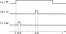
图4为示出了根据第一实施例在从像素P中读取信号时供给到各个单元的脉冲信号的时序图。在图4中,(a)表示选择信号,(b)表示传输信号,并且(c)表示复位信号。 FIG. 4 is a timing chart showing pulse signals supplied to respective units when reading a signal from a pixel P according to the first embodiment. In FIG. 4 , (a) represents a selection signal, (b) represents a transfer signal, and (c) represents a reset signal. the
如图4所示,在第一时刻t1,选择晶体管24导通。接着,在第二时刻t2,复位晶体管25导通。这使得放大晶体管23的栅极电位复位。
As shown in FIG. 4, at a first time t1, the
接着,在第三时刻t3,复位晶体管25截止。随后,与该复位电平对 应的电压被读出到列电路14。
Next, at a third time t3, the
在第四时刻t4,传输晶体管22导通,从而将累积在光电二极管21中的信号电荷传输到放大晶体管23的栅极。
At the fourth time t4 , the
接着,在第五时刻t5,传输晶体管22截止。随后,与累积的信号电荷量对应的信号电平的电压被读出到列电路14。
Next, at the fifth time t5, the
列电路14对首先读出的复位电平和随后读出的信号电平进行减法处理,并且累积信号。因此,消除了例如由各个像素P的晶体管的Vth的变化产生的固定模式噪声。
The
由于晶体管22、24和25的栅极分别以在水平方向x上排列的像素行为单位连接,所以像素的驱动逐行进行,即,同一行的像素同时受到驱动。具体地说,根据由垂直选择电路13供给的选择信号在与水平行(像素行)垂直的方向上逐行选择水平行(像素行)。每个像素的晶体管由从定时控制电路18输出的各种定时信号控制。因此,各个像素的输出信号通过垂直信号线27被逐行读出到列电路14。
Since the gates of the
然后,在列电路14中累积的信号由水平选择电路15选择,并且依次输出到输出电路17。
Then, the signals accumulated in the
(3)固体摄像器件的详细结构 (3) Detailed structure of solid-state imaging device
下面对该实施例的固体摄像器件1的细节进行说明。
Details of the solid-
图5为根据本发明第一实施例的固体摄像器件的截面图。 5 is a cross-sectional view of a solid-state imaging device according to a first embodiment of the present invention. the
该实施例的固体摄像器件1被构成为接收从半导体基板101背侧进入的主光线L以拍摄图像。
The solid-
具体地说,如图5所示,固体摄像器件1包括由n型硅半导体构成的半导体基板101。在半导体基板101上设有埋置氧化物膜30。在埋置氧化物膜30上设有硅膜40。该半导体基板101设有光电二极管21、传输晶体管22、像素晶体管Tr和光电二极管隔离层60。
Specifically, as shown in FIG. 5 , the solid-
像素晶体管Tr包括在图3中所示的放大晶体管23、选择晶体管24和复位晶体管25。放大晶体管23、选择晶体管24和复位晶体管25在图5~图9中共同显示为像素晶体管Tr。
The pixel transistor Tr includes an
埋置氧化物膜30形成在除了形成有下述沟槽RE的区域之外的半导体基板101的整个表面上。硅膜40设置在形成有像素晶体管Tr的区域中的埋置氧化物膜30上。
The buried
(3-1)光电二极管 (3-1) Photodiode
如图5所示,光电二极管21形成在半导体基板101内。光电二极管21接收来自半导体基板101背侧的光,并且将光转换成电荷,从而产生信号电荷。光电二极管21包括n型半导体层10和p型半导体层20。p型半导体层20形成在比形成有n型半导体层10的地方浅的位置处。如图5所示,n型半导体层10与p型半导体层20接触,在光电二极管21中形成pn结。
As shown in FIG. 5 , a
n型半导体层10是通过将n型杂质的离子注入到由n型硅半导体构成的半导体基板101中形成的。因此,在n型半导体层10中的n型杂质的浓度高于在半导体基板101中的n型杂质的浓度。在n型半导体层10中的n型杂质的浓度低于在下述浮动扩散部FD中的n型杂质的浓度。在p型半导体层20中的p型杂质的浓度设定为高于在下述p型半导体区域50和光电二极管隔离层60中的p型杂质的浓度。
The n-
(3-2)晶体管 (3-2) Transistor
例如通过热氧化方法使硅膜40的表面氧化,从而形成由硅氧化物构成的栅极绝缘膜42。在栅极绝缘膜42上形成有像素晶体管Tr即放大晶体管23、选择晶体管24和复位晶体管25的栅极电极Trg。虽然在该图中未示出,但是源极/漏极区域形成在与栅极电极Trg相邻的硅膜40中,并且与栅极电极Trg和栅极绝缘膜42一起形成像素晶体管Tr。
The surface of the
(3-2-1)传输晶体管 (3-2-1) Transfer transistor
如图5所示,传输晶体管22形成在半导体基板101的表面中。传输晶体管22读出由光电二极管21产生的信号电荷。
As shown in FIG. 5 , the
如图5所示,传输晶体管22的传输栅极电极22g从光电二极管21上的埋置氧化物膜30的一部分连续延伸至与光电二极管21相邻的沟槽RE(稍后说明)的一部分。也就是说,传输栅极电极22g以延伸越过台阶的方式从沟道形成区域CH上方延伸至p型半导体层20的一部分,传输 栅极电极22g与沟道形成区域CH之间隔着栅极绝缘膜54(稍后说明)。换句话说,传输栅极电极22g延伸越过位于浮动扩散部FD附近的埋置氧化物膜30被除去了的部分中的栅极绝缘膜54与光电二极管21附近的埋置氧化物膜30的一部分之间的台阶。传输栅极电极22g由扩散有特定导电型杂质的半导体构成。例如,传输栅极电极22g由多晶硅构成。
As shown in FIG. 5 , transfer gate electrode 22 g of
参照图5,浮动扩散部FD形成在半导体基板101的位于沟槽RE下方的表面中,因而浮动扩散部FD与传输栅极电极22g对角地相邻。例如通过将n型杂质注入半导体基板101中,使得在浮动扩散部FD中的n型杂质的浓度高于在n型半导体层10中的n型杂质的浓度,以此来形成浮动扩散部FD。在传输栅极电极22g下方以及在浮动扩散部FD和光电二极管21之间的区域是形成有沟道的沟道形成区域CH。传输晶体管22通过沟道将累积在光电二极管21的n型半导体层10中的信号电荷读出到浮动扩散部FD。换句话说,在该传输晶体管22中,浮动扩散部FD和光电二极管21的n型半导体层10用作一对源极和漏极区域。
Referring to FIG. 5 , the floating diffusion FD is formed in the surface of the
(3-2-2)像素晶体管 (3-2-2) Pixel Transistor
像素晶体管Tr包括在图3中所示的放大晶体管23、选择晶体管24和复位晶体管25。
The pixel transistor Tr includes an
像素晶体管Tr形成在埋置氧化物膜30上。像素晶体管Tr的栅极电极Trg形成在由硅膜40表面上的硅氧化物构成的栅极绝缘膜42上。像素晶体管Tr的源极区域(未图示)和漏极区域(未图示)例如通过将n型杂质注入到硅膜40中形成。
The pixel transistor Tr is formed on the buried
像素晶体管Tr的放大晶体管23、选择晶体管24和复位晶体管25如图3所示一样相互电连接。
The
(3-3)沟槽 (3-3) Groove
沟槽RE形成在半导体基板101中,并且与光电二极管21相邻。例如,通过蚀刻半导体基板101的埋置氧化物膜30和p型半导体层20,使n型半导体层10在沟槽RE底部露出,以此来形成沟槽RE。优选地,沟槽RE足够深,从而使n型半导体层10的表面露出。半导体基板101中的沟槽RE的内表面例如通过热氧化方法氧化,并且由硅氧化物构成的 传输晶体管22的栅极绝缘膜54形成在半导体基板101的在沟槽RE中的表面上。
The trench RE is formed in the
传输栅极电极22g被形成为从沟道形成区域上方的沟槽RE的一部分延伸至p型半导体层20上方。
The transfer gate electrode 22 g is formed to extend from a part of the trench RE above the channel formation region to above the p-
(3-4)p型半导体区域 (3-4) p-type semiconductor region
p型半导体区域50位于沟槽RE下方且在半导体基板101中,并且隔着一个间隙面对浮动扩散部FD。p型半导体区域50例如位于比p型半导体层20更深的位置处。p型半导体区域50形成为其长度等于沟槽RE的宽度,即,等于图5的截面图中的沟道形成区域CH的长度和浮动扩散部FD的长度的总和。
The p-
如果没有设置p型半导体区域50,则具有相同导电型的光电二极管21的电荷累积层和浮动扩散部FD是连通的,与传输晶体管22导通或截止无关。这样,就会难以控制信号电荷的传输。在形成p型半导体区域50时,在电荷累积层和浮动扩散部FD之间形成势垒,由此会使信号电荷的通路(沟道形成区域CH)变窄。因此,当形成p型半导体区域50时,可以通过传输晶体管22的导通和截止来控制信号电荷的传输。
If the p-
可替换地,p型半导体区域50可以比沟槽RE的宽度更长,并且可以与下面说明的光电二极管隔离层60接触。
Alternatively, the p-
(3-5)光电二极管隔离层 (3-5) Photodiode isolation layer
如图5所示,在半导体基板101中形成有用于隔离n型半导体层10的光电二极管隔离层60。例如,光电二极管隔离层60是通过注入p型杂质的离子而形成的。
As shown in FIG. 5 , a
如图5所示,在半导体基板101的前面侧处形成有布线层HL。布线层HL包括埋入在层间绝缘膜Sz中的多个布线H。这些布线分别用作图3所示的传输线26、垂直信号线27、地址线28、复位线29等。
As shown in FIG. 5 , a wiring layer HL is formed at the front side of the
如图5所示,在半导体基板101的背侧处形成有保护膜70。该保护膜70由铪氧化物、氮化硅等构成,并且保护半导体基板101的背面。
As shown in FIG. 5 , a
另外,在半导体基板101上形成有诸如片上透镜(未图示)、滤色器(未 图示)等与像素P相关的光学部件。例如,在该摄像器件是光入射在半导体基板101的背侧上的背照射型摄像器件时,诸如片上透镜、滤色器等光学部件被设在半导体基板101的背侧上。
In addition, optical components related to the pixels P such as on-chip lenses (not shown) and color filters (not shown) are formed on the
(B)制造方法 (B) Manufacturing method
下面对固体摄像器件1的制造方法进行说明。
Next, a method of manufacturing the solid-
图6A~图8C为示出了第一实施例的固体摄像器件的制造方法的各个步骤中的相关部分的截面图。 6A to 8C are cross-sectional views showing relevant parts in respective steps of the method of manufacturing the solid-state imaging device of the first embodiment. the
(1)光电二极管的形成 (1) Formation of photodiodes
首先,参照图6A,以如下方式形成p型半导体层20。
First, referring to FIG. 6A , p-
在形成光电二极管21之前,准备依次层叠有埋置氧化物膜30和硅膜40的半导体基板101。例如,可以采用SOI基板,或者可以采用通过在半导体基板101上层叠埋置氧化物膜30和硅膜40而制备的基板。
Before forming the
参照图6A,通过将p型杂质的离子注入到半导体基板101中,在半导体基板101的表面中形成p型半导体层20,即p+层。该p型半导体层20至少形成在将要形成光电二极管21、沟道形成区域CH和浮动扩散部FD的部分中。
Referring to FIG. 6A , by implanting ions of p-type impurities into the
更具体地说,在通过埋置氧化物膜30和硅膜40注入p型杂质的离子时,选择离子注入的能量,从而在半导体基板101的表面附近形成p型半导体层20。例如,在下面条件下将p型杂质的离子注入到半导体基板101中:
More specifically, when ions of p-type impurities are implanted through buried
注入离子:硼(B) Implanted ions: Boron (B)
注入能量:约50keV Injection energy: about 50keV
杂质浓度:约1×10¹³/cm2 Impurity concentration: about 1×10 13 /cm 2
当在上述条件下将p型杂质的离子注入到半导体基板101中时,形成p型半导体层20。在p型半导体层20中的p型杂质的浓度高于在p型半导体区域50和光电二极管隔离层60中的浓度。
When ions of p-type impurities are implanted into
接着,如图6B所示,通过将p型杂质的离子注入到半导体基板101 中,在半导体基板101中形成光电二极管隔离层60。
Next, as shown in FIG. 6B, by implanting ions of p-type impurities into the
具体地说,通过埋置氧化物膜30和硅膜40在七个分开阶段中将p型杂质的离子注入到半导体基板101的将要形成光电二极管隔离层60的部分中。在改变注入能量的同时在下面条件下进行p型杂质的注入:
Specifically, ions of a p-type impurity are implanted into a portion of
注入离子:硼(B) Implanted ions: Boron (B)
注入能量:约100keV~约3MeV Injection energy: about 100keV ~ about 3MeV
杂质浓度:约2×10¹²/cm2 Impurity concentration: about 2×10 12 /cm 2
光电二极管隔离层60向下形成至距基板表面约4μm的深度处。
The
当在上述条件下将p型杂质的离子注入到半导体基板101中时,形成光电二极管隔离层60。
When ions of p-type impurities are implanted into the
接着,参照图6C,通过将n型杂质的离子注入到半导体基板101中来形成n型半导体层10。该n型半导体层10形成在p型半导体层20下方并且形成在没有形成光电二极管隔离层60的区域中。该n型半导体层10至少形成在将要形成光电二极管21、沟道形成区域CH和浮动扩散部FD的部分中。
Next, referring to FIG. 6C , n-
更具体地说,选择离子注入的能量,使n型半导体层10与p型半导体层20的背侧接触,并且通过埋置氧化物膜30和硅膜40将n型杂质的离子注入到半导体基板101中。例如,在下面的条件下将n型杂质的离子注入到半导体基板101中:
More specifically, the energy of ion implantation is selected such that the n-
注入离子:砷(As) Implanted ions: arsenic (As)
注入能量:约400keV Injection energy: about 400keV
杂质浓度:约4×10¹²/cm2 Impurity concentration: about 4×10 12 /cm 2
当在上述条件下将n型杂质的离子注入到半导体基板101中时,形成n型半导体层10。
When ions of n-type impurities are implanted into
为了使n型半导体层10在背侧方向上扩展,可以进行多次将n型杂质离子注入到半导体基板101中的操作。
In order to expand the n-
(2)晶体管的形成 (2) Formation of transistors
接着,形成在图5中所示的传输晶体管22和像素晶体管Tr。
Next, the
首先,如下面参照图7A所述一样,除去除了要形成像素晶体管Tr的那部分之外的硅膜40。
First, as described below with reference to FIG. 7A , the
也就是说,在要形成像素晶体管Tr的那部分中的硅膜40上形成掩模(未图示)。然后如图7A所示,采用掩模(未图示)蚀刻硅膜40,除去位于除了要形成像素晶体管Tr的部分之外的部分中的硅膜40。随后,除去掩模(未图示)。
That is, a mask (not shown) is formed on the
接着,如下面参照图7B所述一样,形成p型半导体区域50。
Next, as described below with reference to FIG. 7B , a p-
也就是说,在埋置氧化物膜30和硅膜40上形成具有开口的抗蚀剂图形80,使得该开口位于要形成p型半导体区域50的部分处。换句话说,抗蚀剂图形80形成为在要形成沟道形成区域CH和浮动扩散部FD的部分处具有开口。例如,通过采用曝光装置将图形图像曝光到设在半导体基板101上的光致抗蚀剂膜(未图示)上并且将该图形图像显影来形成抗蚀剂图形80。然后,采用抗蚀剂图形80作为掩模,在图7B中的箭头方向上注入p型杂质的离子,从而在半导体基板101中形成p型半导体区域50。
That is, a resist
具体地说,选择离子注入的能量,使p型半导体区域50在半导体基板101中位于比p型半导体层20更深的位置处。例如,在下面条件下将p型杂质的离子注入到半导体基板101中:
Specifically, the energy of ion implantation is selected so that the p-
注入离子:硼(B) Implanted ions: Boron (B)
注入能量:约70keV Injection energy: about 70keV
杂质浓度:约4×10¹²/cm2 Impurity concentration: about 4×10 12 /cm 2
当通过采用抗蚀剂图形80作为掩模在上述条件下注入p型杂质的离子时,在半导体基板101的将要形成沟道形成区域CH和浮动扩散部FD的部分中形成p型半导体区域50。此外,当在上述条件下注入p型杂质的离子时,在p型半导体区域50中的p型杂质的浓度低于在p型半导体层20中的浓度,并且大约与在光电二极管隔离层60中的浓度相等。
When ions of p-type impurities are implanted under the above conditions by using resist
可替换地,p型半导体区域50可以形成为与光电二极管隔离层60 接触或重叠。在这种情况下,在抗蚀剂图形80中形成在光电二极管隔离层60上方延伸的开口,并且通过采用该抗蚀剂图形80作为掩模形成p型半导体区域50。
Alternatively, the p-
接着,如下面参照图7C所述一样,形成沟槽RE。 Next, trench RE is formed as described below with reference to FIG. 7C. the
也就是说,参照图7C,采用用于形成p型半导体区域50的相同抗蚀剂图形80作为掩模,并且蚀刻埋置氧化物膜30和p型半导体层20,从而形成沟槽RE。由于采用抗蚀剂图形80作为掩模,所以沟槽RE形成在要形成沟道形成区域CH和浮动扩散部FD的部分中。例如,进行蚀刻,直到n型半导体层10在沟槽RE的底部露出。
That is, referring to FIG. 7C, the same resist
更具体地说,通过采用抗蚀剂图形80作为掩模将埋置氧化物膜30蚀刻掉。例如,在下面的条件下蚀刻埋置氧化物膜30:
More specifically, buried
蚀刻类型:干式蚀刻 Etching type: dry etching
所采用的气体:CF4 Gas used: CF 4
接着,改变蚀刻条件,并且通过采用抗蚀剂图形80作为掩模来蚀刻在半导体基板101中的p型半导体层20,从而将p型半导体层20向下除去至例如PN结,即n型半导体层10的表面。例如,在下面条件下蚀刻p型半导体层20:
Next, the etching conditions are changed, and the p-
蚀刻类型:干式蚀刻 Etching type: dry etching
所采用的气体:CF4+O2 Gas used: CF 4 +O 2
随后,除去抗蚀剂图形80。因此,p型半导体区域50相对于沟槽RE以自对准方式形成。
Subsequently, the resist
可替换地,在采用抗蚀剂图形80作为掩模蚀刻埋置氧化物膜30之后,可以除去抗蚀剂图形80,并且可以采用埋置氧化物膜30作为掩模将p型半导体层20向下除去至n型半导体层10的表面。
Alternatively, after etching the buried
接着,如下面参照图8A所述一样,形成栅极绝缘膜。 Next, as described below with reference to FIG. 8A, a gate insulating film is formed. the
也就是说,例如通过热处理使硅膜40的表面氧化,从而形成由硅氧化物构成的栅极绝缘膜42。例如通过热处理使除去了p型半导体层20的表面,即在沟槽RE中露出的半导体基板101的表面氧化,从而形成 由硅氧化物构成的栅极绝缘膜54。
That is, the surface of the
接着,如下面参照图8B所述的一样,形成栅极电极,即传输栅极电极22g和栅极电极Trg。 Next, as described below with reference to FIG. 8B , gate electrodes, namely, the transfer gate electrode 22 g and the gate electrode Trg are formed. the
也就是说,形成传输栅极电极22g,使得传输栅极电极22g从沟道形成区域CH上方延伸至在光电二极管21上方的埋置氧化物膜30上表面的一部分,传输栅极电极22g与沟道形成区域CH之间隔着沟槽RE中的栅极绝缘膜54。这里,传输栅极电极22g形成为不与栅极绝缘膜42接触。在形成传输栅极电极22g的同时,在栅极绝缘膜42上形成栅极电极Trg。
That is, the
例如,通过在埋置氧化物膜30、栅极绝缘膜42和栅极绝缘膜54上形成多晶硅膜,并采用具有与栅极电极形成区域对应的图形的光致抗蚀剂(未图示)作为掩模干式蚀刻该多晶硅膜,从而通过图形化来形成传输栅极电极22g和栅极电极Trg。
For example, by forming a polysilicon film on the buried
接着,如下面参照图8C所述一样,形成浮动扩散部FD。 Next, the floating diffusion FD is formed as described below with reference to FIG. 8C . the
也就是说,在图8C中的箭头方向上将n型杂质的离子注入到半导体基板101中,从而在除去了p型半导体层20的,即形成有沟槽RE的半导体基板101的表面上形成浮动扩散部FD。
That is, ions of the n-type impurity are implanted into the
更具体地说,如图8C所示,通过采用抗蚀剂图形90、传输栅极电极22g和埋置氧化物膜30作为掩模,将n型杂质的离子注入到半导体基板101中。因此,该浮动扩散部FD相对于传输栅极电极以自对准的方式,形成在与传输栅极电极22g对角地相邻的半导体基板101的表面区域中。在形成浮动扩散部FD的同时,还在栅极电极Trg的两侧处将n型杂质离子注入到硅膜40中,从而形成像素晶体管Tr的源极区域和漏极区域。例如,在下面的条件下将n型杂质的离子注入到半导体基板101中:
More specifically, as shown in FIG. 8C, ions of n-type impurities are implanted into
注入离子:磷(B) Implanted ions: Phosphorus (B)
注入能量:约10keV Injection energy: about 10keV
注入剂量:约2×10¹⁵原子/cm2 Implantation dose: about 2×10 15 atoms/cm 2
当在上述条件下将n型杂质的离子注入到半导体基板101中时,例如形成浮动扩散部FD。此外,当在上述条件下注入n型杂质的离子时,在浮动扩散部FD中的n型杂质的浓度比在n型半导体层10中的浓度更高。浮动扩散部FD和光电二极管21分别起到传输晶体管22的源极区域和漏极区域的作用。因此,获得传输晶体管22和像素晶体管Tr。随后,除去抗蚀剂图形90。
When ions of n-type impurities are implanted into the
接着,如图9A所示,在晶体管上形成布线层HL和层间绝缘膜Sz。 Next, as shown in FIG. 9A , a wiring layer HL and an interlayer insulating film Sz are formed over the transistor. the
参照图9B,将支撑基板(未图示)粘贴到形成有晶体管的半导体基板101的前侧上。通过例如化学机械研磨(chemical mechanical polishing,CMP)来研磨半导体基板101的背面以减小半导体基板101的厚度。
Referring to FIG. 9B , a support substrate (not shown) is pasted on the front side of the
然后在半导体基板101的研磨表面上形成铪氧化物膜或氮化硅膜,从而形成用于保护半导体基板101背面的保护膜70。因此,获得在图5中所示的固体摄像器件1。
A hafnium oxide film or a silicon nitride film is then formed on the ground surface of the
[C]概要 [C] Summary
如上所述,在该实施例中,传输栅极电极22g隔着栅极绝缘膜54与p型半导体层20相邻。因此,由错位引起的负面效应不会出现。光电二极管21的光电子累积单元是位于p型半导体层20下方的n型半导体层10的一部分。传输栅极电极22g和光电子累积单元之间的位置关系也不会受到错位的影响。在沟道区域中,由于p型半导体层20的端部和p型半导体区域50的端部两者都由沟槽RE限定,所以沟道区域也不会受到错位影响。因此,根据该实施例的制造方法,能够提供可以将信号电荷令人满意地从光电二极管21传输到浮动扩散部FD的固体摄像器件1。
As described above, in this embodiment, the transfer gate electrode 22 g is adjacent to the p-
因此,可以制造出具有高饱和信号电平、高灵敏度和低随机噪声的固体摄像器件1。在采用固体摄像器件1时,可以制造出具有高饱和信号电平、高灵敏度和低随机噪声的电子装置。
Therefore, the solid-
光电二极管21的光电子累积单元隔着栅极绝缘膜54在深度方向和横向方向两个方向上靠近传输栅极电极22g。因此,可以改善将累积在光电二极管21的电荷累积层中的信号电荷传输到浮动扩散部FD的效率,并且可以降低电压。
The photoelectron accumulation unit of the
在该实施例中,光由半导体基板101的背面接收。但是,其它布置也是可能的。即使在主光线L由在形成有像素晶体管和其它相关部件的半导体基板101的前面侧接收时,也能够获得相同的优点。
In this embodiment, light is received by the back surface of the
2.第二实施例 2. The second embodiment
[A]器件结构 [A] Device structure
图10为根据本发明第二实施例的固体摄像器件的截面图。 10 is a cross-sectional view of a solid-state imaging device according to a second embodiment of the present invention. the
如图10所示,该实施例的固体摄像器件1b与第一实施例的不同之处在于传输栅极电极(传输栅极电极22gb)的布置。第二实施例在其它特征方面与第一实施例相同。因此,将该说明简化以避免重复。
As shown in FIG. 10, the solid-
如图10所示,传输栅极电极22gb形成在栅极绝缘膜54b上,并且从沟槽REb的一部分连续延伸至光电二极管21b的p型半导体层20b的上表面。换句话说,传输栅极电极22gb从沟道形成区域CHb上方连续延伸至p型半导体层20b上方,传输栅极电极22gb与沟道形成区域CHb之间隔着栅极绝缘膜54b。除此之外,该固体摄像器件1b具有与第一实施例相同的结构。
As shown in FIG. 10 , transfer gate electrode 22gb is formed on
在该实施例中,传输栅极电极22gb没有形成在埋置氧化物膜30b上,而是形成在p型半导体层20b上方的栅极绝缘膜54b上。因此,传输栅极电极22gb所延伸越过的台阶变得低于第一实施例中的台阶。因此,增大了栅极蚀刻裕度,并且由于能够很容易地除去留在台阶部分中的栅极材料,所以可以简化制造过程。
In this embodiment, transfer gate electrode 22gb is not formed on buried
[B]制造方法 [B] Manufacturing method
下面对固体摄像器件1b的制造方法进行说明。
Next, a method of manufacturing the solid-
图11A~图11C为示出了在第二实施例的固体摄像器件的制造方法的各个步骤中的相关部分的截面图。 11A to 11C are cross-sectional views showing relevant parts in respective steps of the method of manufacturing the solid-state imaging device of the second embodiment. the
直到形成沟槽RE的步骤的那些步骤都与第一实施例相同,因此不再说明。 The steps up to the step of forming the trench RE are the same as those of the first embodiment, and thus will not be described again. the
如下面参照图11A所述一样,除去埋置氧化物膜30b。这里,至少除去在要形成传输栅极电极22gb的区域中的埋置氧化物膜30b。
也就是说,首先如图11A所示,形成具有开口的抗蚀剂图形90b,该开口具有埋置氧化物膜30b将要被除去的部分的形状,使得该开口出现在该部分中。例如,通过采用曝光装置将图形图像曝光到设在半导体基板101b上的光致抗蚀剂膜(未图示)上并使图形图像显影,从而形成抗蚀剂图形90b。
That is, first, as shown in FIG. 11A, a resist
然后如图11A所示,采用抗蚀剂图形90b作为掩模来蚀刻埋置氧化物膜30b,除去埋置氧化物膜30b的特定部分。随后,除去抗蚀剂图形90b。因此,形成沟槽REb。
Then, as shown in FIG. 11A, the buried
接着,参照图11B,与在第一实施例中相同,形成栅极绝缘膜,即栅极绝缘膜42b和栅极绝缘膜54b。
Next, referring to FIG. 11B , as in the first embodiment, gate insulating films, namely,
然后,如下面参照图11C所述一样,形成栅极电极,即传输栅极电极22gb和像素晶体管Trb的栅极电极Trgb。 Then, as described below with reference to FIG. 11C , the gate electrodes, that is, the transfer gate electrode 22gb and the gate electrode Trgb of the pixel transistor Trb are formed. the
也就是说,在栅极绝缘膜54b上形成传输栅极电极22gb,使传输栅极电极22gb从沟道形成区域CHb上方延伸至光电二极管21b的p型半导体层20b上方,同时避免与栅极绝缘膜42b接触。在形成传输栅极电极22gb的同时,在栅极绝缘膜42b上的栅极电极形成区域中形成栅极电极Trgb。形成传输栅极电极22gb和栅极电极Trgb的过程与第一实施例相同。
That is, the transfer gate electrode 22gb is formed on the
随后,与在第一实施例中相同,形成浮动扩散部FDb、布线层HLb、层间绝缘膜Szb和保护膜70b,从而完成图10中所示的固体摄像器件1b的制造。
Subsequently, as in the first embodiment, the floating diffusion FDb, the wiring layer HLb, the interlayer insulating film Szb, and the
[C]概要 [C] Summary
在该实施例中,除了传输栅极电极22gb之外,所有部件与在第一实施例中一样形成。 In this embodiment, all components are formed as in the first embodiment except for the transfer gate electrode 22gb. the
因此,与在第一实施例中相同,可以制造出能够将信号电荷令人满意地从光电二极管21b传输到浮动扩散部FDb的固体摄像器件1b。因此,能够制造出具有高饱和信号电平、高灵敏度和低随机噪声的固体摄像器件1b。在采用该固体摄像器件1b时,可以制造出具有高饱和信号电平、高灵敏度和低随机噪声的电子装置。
Therefore, as in the first embodiment, the solid-
此外,由于传输栅极电极22gb形成在p型半导体层20b上,而不是形成在埋置氧化物膜30b上,所以传输栅极电极22gb所延伸越过的台阶变得低于在第一实施例中的台阶。因此,可以增加栅极蚀刻裕度,并且由于可以很容易地除去留在台阶部分中的栅极材料,所以可以简化制造过程。
Furthermore, since the transfer gate electrode 22gb is formed on the p-
3.第三实施例 3. The third embodiment
[A]器件结构 [A] Device structure
图12为根据本发明第三实施例的固体摄像器件的截面图。 12 is a cross-sectional view of a solid-state imaging device according to a third embodiment of the present invention. the
如图12所示,该实施例的固体摄像器件1c与第一实施例的不同之处在于传输栅极电极(传输栅极电极22gc)的布置。该第三实施例在其它特征方面与第一实施例相同。因此,将该说明简化以避免重复。
As shown in FIG. 12, the solid-
如图12所示,传输栅极电极22gc从沟道形成区域CHc上方的栅极绝缘膜54c的一部分连续延伸至光电二极管21c上方的硅膜40c上的栅极绝缘膜42c的一部分。除此之外,固体摄像器件1c具有与第一实施例相同的结构。
As shown in FIG. 12 , the transfer gate electrode 22gc continuously extends from a part of the
在该实施例中,传输栅极电极22gc没有形成在埋置氧化物膜30c上,而是形成在栅极绝缘膜42c上。与第一实施例的固体摄像器件1相比,能够由此进一步减小该实施例的固体摄像器件1c的尺寸。
In this embodiment, transfer gate electrode 22gc is not formed on buried
[B]制造方法 [B] Manufacturing method
下面对固体摄像器件1c的制造方法进行说明。
Next, a method of manufacturing the solid-
图13A~图14B为示出了第三实施例的固体摄像器件的制造方法的各个步骤中的相关部分的截面图。 13A to 14B are cross-sectional views showing relevant parts in respective steps of the method of manufacturing the solid-state imaging device of the third embodiment. the
直到形成像素晶体管Trc的步骤的那些步骤都与第一实施例相同,因此不再说明。 Those steps up to the step of forming the pixel transistor Trc are the same as those of the first embodiment, and thus will not be described again. the
接着,如下面参照图13A所述一样,形成p型半导体区域50c。
Next, as described below with reference to FIG. 13A, a p-
也就是说,形成具有开口的抗蚀剂图形80c,该开口具有要形成p型半导体区域50c的部分的形状,使得该开口布置成在该部分处出现。换句话说,抗蚀剂图形80c形成为使要形成沟道形成区域CHc和浮动扩 散部FDc的部分露出。另外,抗蚀剂图形80c形成为使得硅膜40c的开口侧的侧面形成抗蚀剂图形80c的开口的侧壁。形成抗蚀剂图形80c的过程与第一实施例相同。
That is, a resist
采用抗蚀剂图形80c作为掩模,在图13A中的箭头方向上注入p型杂质的离子,从而在半导体基板101c中形成p型半导体区域50c。离子注入的过程与第一实施例相同。
Using the resist
接着,如图13B所示,通过与在第一实施例中相同的过程形成沟槽REc。因此,p型半导体区域50c相对于沟槽REc以自对准的方式形成。
Next, as shown in FIG. 13B, the trench REc is formed by the same process as in the first embodiment. Therefore, the p-
接着,如图14A所示,通过与在第一实施例中相同的过程形成栅极绝缘膜,即栅极绝缘膜42c和栅极绝缘膜54c。
Next, as shown in FIG. 14A , gate insulating films, that is, a
接着,如下面参照图14B所述一样,形成栅极电极,即传输栅极电极22gc和栅极电极Trgc。 Next, as described below with reference to FIG. 14B , gate electrodes, that is, transfer gate electrode 22gc and gate electrode Trgc are formed. the
也就是说,形成传输栅极电极22gc,使得传输栅极电极22gc从在沟道形成区域CHc上方的沟槽REc中的栅极绝缘膜54c的一部分延伸至在硅膜40c的上表面上的栅极绝缘膜42c的一部分,同时避免与栅极电极Trgc接触。在形成传输栅极电极22gc的同时,在栅极绝缘膜42c上的栅极电极形成区域中形成栅极电极Trgc。形成传输栅极电极22gc和栅极电极Trgc的过程与第一实施例相同。
That is, the transfer gate electrode 22gc is formed so that the transfer gate electrode 22gc extends from a part of the
随后,与在第一实施例中相同,形成浮动扩散部FDc、布线层HLc、层间绝缘膜Szc和保护膜70c,从而完成图12中所示的固体摄像器件1c的制造。
Subsequently, as in the first embodiment, the floating diffusion FDc, the wiring layer HLc, the interlayer insulating film Szc, and the
[C]概要 [C] Summary
在该实施例中,除了传输栅极电极22gc之外,所有部件与在第一实施例中一样形成。 In this embodiment, all components are formed as in the first embodiment except for the transfer gate electrode 22gc. the
因此,与在第一实施例中相同,可以制造出能够通过传输栅极电极22gc将信号电荷令人满意地从光电二极管21c传输到浮动扩散部FDc的固体摄像器件1c。
Therefore, as in the first embodiment, the solid-
因此,能够制造出具有高饱和信号电平、高灵敏度和低随机噪声的 固体摄像器件1c。在采用该固体摄像器件1c时,可以制造出具有高饱和信号电平、高灵敏度和低随机噪声的电子装置。
Therefore, a solid-
由于传输栅极电极22gc形成在硅膜40c上,所以能够使固体摄像器件1c的面积减小,减小的面积为第一实施例中使埋置氧化物膜30露出的那部分的面积。因此,可以减小固体摄像器件1c的尺寸。
Since the transfer gate electrode 22gc is formed on the
4.第四实施例 4. The fourth embodiment
[A]器件结构 [A] Device structure
图15~图17为示出了根据本发明第四实施例的固体摄像器件1d的相关部分的示意图。
15 to 17 are schematic diagrams showing relevant parts of a solid-
如图16所示,该实施例的固体摄像器件1d与第一实施例的不同之处在于光电二极管21d和传输电极22gd的布置。除此之外,第四实施例与第一实施例相同。因此,将该说明简化以避免重复。
As shown in FIG. 16, the solid-
图15为摄像区域PA的俯视图。图16为沿图15中的XVI-XVI线的摄像区域PA的截面图。图17示出了设在摄像区域PA中的像素P的电路结构。 FIG. 15 is a plan view of the imaging area PA. FIG. 16 is a cross-sectional view of the imaging area PA along line XVI-XVI in FIG. 15 . FIG. 17 shows a circuit configuration of a pixel P provided in the imaging area PA. the
下面说明固体摄像器件1d的各个部件。
Each component of the solid-
(1)光电二极管 (1) Photodiode
固体摄像器件1d包括按照与在图2中所示的方式相同的方式布置在信号读出面(xy表面)上的多个光电二极管21d。光电二极管21d以规则间距在水平方向x和与水平方向x垂直的垂直方向y上排列,与像素P的布置对应。
The solid-
在该实施例中,如图15和图16所示,各个光电二极管21d设有传输晶体管22d。传输晶体管22d与光电二极管21d相邻。光电二极管21d被布置成使一对光电二极管21d夹着一个浮动扩散部FDd。在该实施例中,相对于水平方向x和垂直方向y对角地排列的两个光电二极管21d被布置成夹着一个浮动扩散部FDd。
In this embodiment, as shown in FIGS. 15 and 16, each
如图17所示,四个光电二极管21d构成为共用一组放大晶体管23d、选择晶体管24d和复位晶体管25d。四个传输晶体管22d形成为用于四个 光电二极管21d。两个光电二极管21d和两个传输晶体管22d形成为共用一个浮动扩散部FDd。
As shown in FIG. 17, four
如图17所示,一个放大晶体管23d、一个选择晶体管24d以及一个复位晶体管25d被设置为用于四个光电二极管21d。
As shown in FIG. 17, one
(2)传输晶体管 (2) Transfer transistor
如图15所示,多个传输晶体管22d形成为与像素P对应。传输晶体管22d被布置为,在设置在相对于水平方向x和垂直方向y对角地排列的像素P之间的浮动扩散部FDd由两个传输晶体管22d夹着。
As shown in FIG. 15 , a plurality of
如图16所示,传输晶体管22d的传输栅极电极22gd从在沟道形成区域CHd上方的栅极绝缘膜54d的一部分延伸至在光电二极管21d上的埋置氧化物膜30d的一部分。如图16所示,传输晶体管22d的传输栅极电极22gd在半导体基板101d的表面中与浮动扩散部FDd对角地相邻。一对传输栅极电极22gd夹着一个浮动扩散部FDd。
As shown in FIG. 16 , the transfer gate electrode 22gd of the
在该实施例中,如图17所示,各个传输晶体管22d的一个端子与光电二极管21d的阴极电连接,并且另一个端子与浮动扩散部FDd电连接。具体地说,一对传输晶体管电连接至一个浮动扩散部FDd。另一对传输晶体管电连接至另一个浮动扩散部FDd。
In this embodiment, as shown in FIG. 17, one terminal of each
(3)像素晶体管 (3) Pixel transistor
如图15所示,在垂直方向y上排列的多个光电二极管21d之间设有像素晶体管Trd,该像素晶体管Trd包括放大晶体管23d、选择晶体管24d和复位晶体管25d。
As shown in FIG. 15, a pixel transistor Trd including an
在该实施例中,如图17所示,放大晶体管23d、选择晶体管24d和复位晶体管25d被一组光电二极管21d共用。更具体地说,如图17所示,一个放大晶体管23d、一个选择晶体管24d和一个复位晶体管25d被设置为用于每组四个光电二极管21d。因此,该实施例的固体摄像器件1d的尺寸与第一实施例的固体摄像器件1相比可以进一步减小。
In this embodiment, as shown in FIG. 17, the
[B]制造方法 [B] Manufacturing method
下面说明固体摄像器件1d的制造方法。
Next, a method of manufacturing the solid-
图18A和图18B为示出了在第四实施例的固体摄像器件的制造方法的各个步骤中的相关部分的截面图。 18A and 18B are cross-sectional views showing relevant parts in respective steps of the method of manufacturing the solid-state imaging device of the fourth embodiment. the
直到形成栅极绝缘膜的步骤的那些步骤都与第一实施例相同,因此不再说明。 Those steps up to the step of forming the gate insulating film are the same as those of the first embodiment, and thus will not be described again. the
如下面参照图18A所述一样,接着形成栅极电极,即传输栅极电极22gd和栅极电极Trgd。 As described below with reference to FIG. 18A , the gate electrodes, ie, the transfer gate electrode 22gd and the gate electrode Trgd are formed next. the
也就是说,形成传输栅极电极22gd,使得传输栅极电极22gd从在沟道形成区域CHd上方的位于沟槽REd中的栅极绝缘膜54d的一部分延伸至在光电二极管21d上的埋置氧化物膜30d上表面的一部分。在形成传输栅极电极22gd的同时,在栅极绝缘膜42d上的栅极电极形成区域中形成栅极电极Trgd。形成传输栅极电极22gd和栅极电极Trgd的过程与第一实施例相同。
That is, the transfer gate electrode 22gd is formed so that the transfer gate electrode 22gd extends from a part of the
接着,如图18B所示,通过在图18B中的箭头方向上将n型杂质的离子注入到除去了p型半导体层20d的半导体基板101d中,从而在半导体基板101d的表面中形成浮动扩散部FDd。
Next, as shown in FIG. 18B, a floating diffusion is formed in the surface of the
更具体地说,如图18B所示,通过采用抗蚀剂图形90d、传输栅极电极22gd和埋置氧化物膜30d作为掩模,将n型杂质的离子注入到半导体基板101d中。因此,浮动扩散部FDd形成在半导体基板101d的表面区域中,与一对传输栅极电极22gd中的各个传输栅极电极22gd相邻。同时,也在栅极电极Trgd的两侧处将n型杂质离子注入到硅膜40d中,以便形成像素晶体管Trdg的源极区域和漏极区域。离子注入的条件与在第一实施例中的那些相同。
More specifically, as shown in FIG. 18B, ions of n-type impurities are implanted into the
随后,如图18A和图18B所示一样,如在第一实施例中相同形成布线层HLd、层间绝缘膜Szd和保护膜70d,从而完成固体摄像器件1d的制造过程。
Subsequently, as shown in FIGS. 18A and 18B , the wiring layer HLd, the interlayer insulating film Szd, and the
[C]概要 [C] Summary
在该实施例中,除了光电二极管21d和传输栅极电极22gd布置的数量,所有部件与在第一实施例中一样形成。
In this embodiment, all components are formed as in the first embodiment except for the number of arrangements of the
因此,与在第一实施例中相同,可以制造出能够通过传输栅极电极22gd将信号电荷令人满意地从光电二极管21d传输到浮动扩散部FDd的固体摄像器件1d。
Therefore, as in the first embodiment, the solid-
因此,能够制造出具有高饱和信号电平、高灵敏度和低随机噪声的固体摄像器件1d。在采用固体摄像器件1d时,可以制造出具有高饱和信号电平、高灵敏度和低随机噪声的电子装置。
Therefore, it is possible to manufacture a solid-
在该实施例中,四个传输晶体管被设置为用于四个光电二极管。一个放大晶体管23d、一个选择晶体管24d和一个复位晶体管25d被设置为用于四个光电二极管21d。因此,可以减小固体摄像器件1d的尺寸。
In this embodiment, four transfer transistors are provided for four photodiodes. One
在实施本发明时,可以采用上述实施例的各种变形和变化。例如,p型半导体区域可以具有除了上述实施例的那些结构之外的结构。 Various modifications and variations of the above-described embodiments may be employed in practicing the invention. For example, the p-type semiconductor region may have structures other than those of the above-described embodiments. the
图19为示出了p型半导体区域50的变形的截面图。如图19所示,p型半导体区域50可以在深度方向上从沟槽RE下方延伸。
FIG. 19 is a cross-sectional view showing deformation of the p-
根据该结构,在传输晶体管22截止时,光电二极管21和浮动扩散部FD是不连通的。在传输晶体管22导通时,在沟道形成区域CH中形成沟道,并且光电二极管21和浮动扩散部FD连通。
According to this structure, when the
虽然在这些实施例中说明了在背侧接收主光线L的固体摄像器件,但是结构不限于此。通过在前侧接收主光线L的固体摄像器件可以实现相同的优点。 Although the solid-state imaging device receiving the chief ray L on the backside has been described in these embodiments, the structure is not limited thereto. The same advantages can be achieved by a solid-state imaging device that receives the chief ray L on the front side. the
应该指出的是,在上述实施例中,半导体基板101、101b、101c和101d为根据本发明的半导体基板的非限定性示例。n型半导体层10为本发明第二区域的非限定性示例。p型半导体层20为根据本发明的第一区域的非限定性示例。光电二极管21、21b、21c和21d为根据本发明的光电转换单元的非限定性示例。传输晶体管22、22b、22c和22d为根据本发明的传输晶体管的非限定性示例。传输栅极电极22g、22gb、22gc和22gd为根据本发明的传输栅极电极的非限定性示例。像素晶体管Tr、Trb、Trc和Trd为根据本发明的晶体管的非限定性示例。抗蚀剂图形80和80c为根据本发明的抗蚀剂图形的非限定性示例。p型半导体区域50和50c为根据本发明的第三区域的非限定性示例。埋置氧化物膜30和30d为根 据本发明的绝缘膜的非限定性示例。硅膜40、40c和40d为根据本发明的半导体层的非限定性示例。栅极绝缘膜54、54b、54c和54d为根据本发明的栅极绝缘膜的非限定性示例。沟道形成区域CH、CHb、CHc和CHd为根据本发明的沟道区域的非限定性示例。浮动扩散部FD、FDb、FDc和FDd为根据本发明的读出漏极的非限定性示例。
It should be noted that in the above-mentioned embodiments, the
本领域技术人员应当理解,依据设计要求和其它因素,可以在本发明所附的权利要求及其等同物的范围内进行各种修改、组合、次组合及改变。 It should be understood by those skilled in the art that various modifications, combinations, sub-combinations and changes can be made within the scope of the appended claims of the present invention and their equivalents according to design requirements and other factors. the
Claims (13)
Applications Claiming Priority (2)
| Application Number | Priority Date | Filing Date | Title |
|---|---|---|---|
| JP2009-191133 | 2009-08-20 | ||
| JP2009191133A JP5487798B2 (en) | 2009-08-20 | 2009-08-20 | Solid-state imaging device, electronic apparatus, and manufacturing method of solid-state imaging device |
Publications (2)
| Publication Number | Publication Date |
|---|---|
| CN101997015A CN101997015A (en) | 2011-03-30 |
| CN101997015B true CN101997015B (en) | 2012-11-28 |
Family
ID=43604618
Family Applications (1)
| Application Number | Title | Priority Date | Filing Date |
|---|---|---|---|
| CN201010250753.XA Expired - Fee Related CN101997015B (en) | 2009-08-20 | 2010-08-11 | Solid-state imaging device, method for manufacturing sol-state imaging device and electronic apparatus |
Country Status (5)
| Country | Link |
|---|---|
| US (1) | US8399914B2 (en) |
| JP (1) | JP5487798B2 (en) |
| KR (1) | KR20110019702A (en) |
| CN (1) | CN101997015B (en) |
| TW (1) | TWI455295B (en) |
Families Citing this family (12)
| Publication number | Priority date | Publication date | Assignee | Title |
|---|---|---|---|---|
| JP6327779B2 (en) * | 2012-02-29 | 2018-05-23 | キヤノン株式会社 | Photoelectric conversion device, focus detection device, and imaging system |
| JP2014022561A (en) | 2012-07-18 | 2014-02-03 | Sony Corp | Solid-state imaging device and electronic apparatus |
| KR102087233B1 (en) * | 2013-01-17 | 2020-03-10 | 삼성전자주식회사 | Semiconductor cmos image sensor(cis) having vertical transfer gate (vtg) and a method for production thereof |
| JP2014199898A (en) * | 2013-03-11 | 2014-10-23 | ソニー株式会社 | Solid-state imaging element and method of manufacturing the same, and electronic equipment |
| KR20150061074A (en) * | 2013-11-25 | 2015-06-04 | 에스케이하이닉스 주식회사 | Image sensor and method for fabricating the same |
| EP3358827A4 (en) * | 2015-09-30 | 2019-11-27 | Nikon Corporation | IMAGE CAPTURE ELEMENT AND ELECTRONIC CAMERA |
| KR102661038B1 (en) * | 2016-02-09 | 2024-04-26 | 소니그룹주식회사 | Semiconductor devices and manufacturing methods of semiconductor devices and solid-state imaging devices and electronic devices |
| CN109564924A (en) * | 2016-04-21 | 2019-04-02 | Towerjazz松下半导体有限公司 | Solid-state image photographic device and its manufacturing method |
| CN110970453B (en) * | 2018-10-01 | 2024-10-08 | 松下知识产权经营株式会社 | Camera device |
| JP2021019171A (en) * | 2019-07-24 | 2021-02-15 | ソニーセミコンダクタソリューションズ株式会社 | Solid-state imaging device and electronic apparatus |
| WO2023190407A1 (en) * | 2022-03-29 | 2023-10-05 | ラピスセミコンダクタ株式会社 | Semiconductor device and solid-state imaging device |
| JPWO2023190406A1 (en) * | 2022-03-29 | 2023-10-05 |
Citations (2)
| Publication number | Priority date | Publication date | Assignee | Title |
|---|---|---|---|---|
| CN1467856A (en) * | 2002-06-10 | 2004-01-14 | ������������ʽ���� | Semiconductor device and manufacturing method thereof |
| CN101136425A (en) * | 2006-08-29 | 2008-03-05 | 索尼株式会社 | Solid-state imaging device and imaging device |
Family Cites Families (11)
| Publication number | Priority date | Publication date | Assignee | Title |
|---|---|---|---|---|
| US5466612A (en) * | 1992-03-11 | 1995-11-14 | Matsushita Electronics Corp. | Method of manufacturing a solid-state image pickup device |
| US6023081A (en) * | 1997-11-14 | 2000-02-08 | Motorola, Inc. | Semiconductor image sensor |
| JP3840214B2 (en) * | 2003-01-06 | 2006-11-01 | キヤノン株式会社 | Photoelectric conversion device, method for manufacturing photoelectric conversion device, and camera using the same |
| JP4439888B2 (en) * | 2003-11-27 | 2010-03-24 | イノテック株式会社 | MOS type solid-state imaging device and driving method thereof |
| JP2005311496A (en) * | 2004-04-19 | 2005-11-04 | Sony Corp | Solid-state imaging apparatus |
| US20050274994A1 (en) * | 2004-06-14 | 2005-12-15 | Rhodes Howard E | High dielectric constant spacer for imagers |
| KR100630704B1 (en) * | 2004-10-20 | 2006-10-02 | 삼성전자주식회사 | CMOS Image Sensor with Nonplanar Transistors and Manufacturing Method Thereof |
| JP4725095B2 (en) * | 2004-12-15 | 2011-07-13 | ソニー株式会社 | Back-illuminated solid-state imaging device and manufacturing method thereof |
| JP2007096271A (en) * | 2005-09-05 | 2007-04-12 | Toshiba Corp | Solid-state imaging device and manufacturing method thereof |
| US7344910B2 (en) * | 2005-09-27 | 2008-03-18 | Omnivision Technologies, Inc. | Self-aligned photodiode for CMOS image sensor and method of making |
| JP2009140983A (en) * | 2007-12-04 | 2009-06-25 | Panasonic Corp | Solid-state imaging device |
-
2009
- 2009-08-20 JP JP2009191133A patent/JP5487798B2/en not_active Expired - Fee Related
-
2010
- 2010-07-28 TW TW099124978A patent/TWI455295B/en not_active IP Right Cessation
- 2010-08-02 KR KR1020100074658A patent/KR20110019702A/en not_active Withdrawn
- 2010-08-11 CN CN201010250753.XA patent/CN101997015B/en not_active Expired - Fee Related
- 2010-08-11 US US12/854,597 patent/US8399914B2/en not_active Expired - Fee Related
Patent Citations (2)
| Publication number | Priority date | Publication date | Assignee | Title |
|---|---|---|---|---|
| CN1467856A (en) * | 2002-06-10 | 2004-01-14 | ������������ʽ���� | Semiconductor device and manufacturing method thereof |
| CN101136425A (en) * | 2006-08-29 | 2008-03-05 | 索尼株式会社 | Solid-state imaging device and imaging device |
Also Published As
| Publication number | Publication date |
|---|---|
| TWI455295B (en) | 2014-10-01 |
| KR20110019702A (en) | 2011-02-28 |
| US8399914B2 (en) | 2013-03-19 |
| US20110042723A1 (en) | 2011-02-24 |
| TW201117364A (en) | 2011-05-16 |
| CN101997015A (en) | 2011-03-30 |
| JP2011044548A (en) | 2011-03-03 |
| JP5487798B2 (en) | 2014-05-07 |
Similar Documents
| Publication | Publication Date | Title |
|---|---|---|
| CN101997015B (en) | Solid-state imaging device, method for manufacturing sol-state imaging device and electronic apparatus | |
| US11729530B2 (en) | Solid-state imaging device, method of manufacturing solid-state imaging device, and electronic apparatus | |
| JP5564909B2 (en) | SOLID-STATE IMAGING DEVICE, ITS MANUFACTURING METHOD, AND ELECTRONIC DEVICE | |
| CN101800231B (en) | Method of manufacturing photoelectric conversion device | |
| TW201630173A (en) | Solid-state imaging device and method of manufacturing solid-state imaging device | |
| KR100832721B1 (en) | Manufacturing Method of CMOS Image Sensor | |
| TWI505454B (en) | Solid-state image pickup device and driving method thereof, manufacturing method of solid-state image pickup device, and electronic information machine | |
| CN102549748B (en) | Solid-state image pickup and manufacture method thereof | |
| JP2017195215A (en) | Image sensor and manufacturing method thereof | |
| US6207984B1 (en) | CMOS sensor | |
| US20070069259A1 (en) | CMOS image sensor and method of manufacturing the same | |
| JP4115446B2 (en) | Manufacturing method of CMOS image sensor | |
| JP2014127514A (en) | Solid-state imaging element, method for manufacturing solid-state imaging element, and electronic equipment | |
| JP2006041080A (en) | Solid-state imaging apparatus | |
| JP2006066710A (en) | Solid state imaging apparatus and manufacturing method thereof | |
| JP2010080739A (en) | Solid-state imaging device, semiconductor device, and methods of manufacturing the devices | |
| JP2005136279A (en) | Manufacturing method of solid state imaging device | |
| JP2013211295A (en) | Solid state image pickup device and method of manufacturing the same, and electronic equipment |
Legal Events
| Date | Code | Title | Description |
|---|---|---|---|
| C06 | Publication | ||
| PB01 | Publication | ||
| C10 | Entry into substantive examination | ||
| SE01 | Entry into force of request for substantive examination | ||
| C14 | Grant of patent or utility model | ||
| GR01 | Patent grant | ||
| CF01 | Termination of patent right due to non-payment of annual fee |
Granted publication date: 20121128 Termination date: 20150811 |
|
| EXPY | Termination of patent right or utility model |