CN101976018B - Photo-mask and manufacturing method thereof - Google Patents
Photo-mask and manufacturing method thereof Download PDFInfo
- Publication number
- CN101976018B CN101976018B CN2010105224975A CN201010522497A CN101976018B CN 101976018 B CN101976018 B CN 101976018B CN 2010105224975 A CN2010105224975 A CN 2010105224975A CN 201010522497 A CN201010522497 A CN 201010522497A CN 101976018 B CN101976018 B CN 101976018B
- Authority
- CN
- China
- Prior art keywords
- pattern
- mentioned
- numbered
- odd
- area
- Prior art date
- Legal status (The legal status is an assumption and is not a legal conclusion. Google has not performed a legal analysis and makes no representation as to the accuracy of the status listed.)
- Expired - Fee Related
Links
Images


Classifications
-
- G—PHYSICS
- G02—OPTICS
- G02B—OPTICAL ELEMENTS, SYSTEMS OR APPARATUS
- G02B17/00—Systems with reflecting surfaces, with or without refracting elements
- G02B17/08—Catadioptric systems
- G02B17/0804—Catadioptric systems using two curved mirrors
-
- G—PHYSICS
- G03—PHOTOGRAPHY; CINEMATOGRAPHY; ANALOGOUS TECHNIQUES USING WAVES OTHER THAN OPTICAL WAVES; ELECTROGRAPHY; HOLOGRAPHY
- G03F—PHOTOMECHANICAL PRODUCTION OF TEXTURED OR PATTERNED SURFACES, e.g. FOR PRINTING, FOR PROCESSING OF SEMICONDUCTOR DEVICES; MATERIALS THEREFOR; ORIGINALS THEREFOR; APPARATUS SPECIALLY ADAPTED THEREFOR
- G03F7/00—Photomechanical, e.g. photolithographic, production of textured or patterned surfaces, e.g. printing surfaces; Materials therefor, e.g. comprising photoresists; Apparatus specially adapted therefor
- G03F7/70—Microphotolithographic exposure; Apparatus therefor
- G03F7/70216—Mask projection systems
- G03F7/70275—Multiple projection paths, e.g. array of projection systems, microlens projection systems or tandem projection systems
-
- G—PHYSICS
- G03—PHOTOGRAPHY; CINEMATOGRAPHY; ANALOGOUS TECHNIQUES USING WAVES OTHER THAN OPTICAL WAVES; ELECTROGRAPHY; HOLOGRAPHY
- G03F—PHOTOMECHANICAL PRODUCTION OF TEXTURED OR PATTERNED SURFACES, e.g. FOR PRINTING, FOR PROCESSING OF SEMICONDUCTOR DEVICES; MATERIALS THEREFOR; ORIGINALS THEREFOR; APPARATUS SPECIALLY ADAPTED THEREFOR
- G03F7/00—Photomechanical, e.g. photolithographic, production of textured or patterned surfaces, e.g. printing surfaces; Materials therefor, e.g. comprising photoresists; Apparatus specially adapted therefor
- G03F7/70—Microphotolithographic exposure; Apparatus therefor
- G03F7/70216—Mask projection systems
- G03F7/70358—Scanning exposure, i.e. relative movement of patterned beam and workpiece during imaging
-
- G—PHYSICS
- G03—PHOTOGRAPHY; CINEMATOGRAPHY; ANALOGOUS TECHNIQUES USING WAVES OTHER THAN OPTICAL WAVES; ELECTROGRAPHY; HOLOGRAPHY
- G03F—PHOTOMECHANICAL PRODUCTION OF TEXTURED OR PATTERNED SURFACES, e.g. FOR PRINTING, FOR PROCESSING OF SEMICONDUCTOR DEVICES; MATERIALS THEREFOR; ORIGINALS THEREFOR; APPARATUS SPECIALLY ADAPTED THEREFOR
- G03F7/00—Photomechanical, e.g. photolithographic, production of textured or patterned surfaces, e.g. printing surfaces; Materials therefor, e.g. comprising photoresists; Apparatus specially adapted therefor
- G03F7/70—Microphotolithographic exposure; Apparatus therefor
- G03F7/70691—Handling of masks or workpieces
- G03F7/70716—Stages
- G03F7/70725—Stages control
-
- G—PHYSICS
- G03—PHOTOGRAPHY; CINEMATOGRAPHY; ANALOGOUS TECHNIQUES USING WAVES OTHER THAN OPTICAL WAVES; ELECTROGRAPHY; HOLOGRAPHY
- G03F—PHOTOMECHANICAL PRODUCTION OF TEXTURED OR PATTERNED SURFACES, e.g. FOR PRINTING, FOR PROCESSING OF SEMICONDUCTOR DEVICES; MATERIALS THEREFOR; ORIGINALS THEREFOR; APPARATUS SPECIALLY ADAPTED THEREFOR
- G03F7/00—Photomechanical, e.g. photolithographic, production of textured or patterned surfaces, e.g. printing surfaces; Materials therefor, e.g. comprising photoresists; Apparatus specially adapted therefor
- G03F7/70—Microphotolithographic exposure; Apparatus therefor
- G03F7/70691—Handling of masks or workpieces
- G03F7/70791—Large workpieces, e.g. glass substrates for flat panel displays or solar panels
-
- G—PHYSICS
- G03—PHOTOGRAPHY; CINEMATOGRAPHY; ANALOGOUS TECHNIQUES USING WAVES OTHER THAN OPTICAL WAVES; ELECTROGRAPHY; HOLOGRAPHY
- G03F—PHOTOMECHANICAL PRODUCTION OF TEXTURED OR PATTERNED SURFACES, e.g. FOR PRINTING, FOR PROCESSING OF SEMICONDUCTOR DEVICES; MATERIALS THEREFOR; ORIGINALS THEREFOR; APPARATUS SPECIALLY ADAPTED THEREFOR
- G03F9/00—Registration or positioning of originals, masks, frames, photographic sheets or textured or patterned surfaces, e.g. automatically
- G03F9/70—Registration or positioning of originals, masks, frames, photographic sheets or textured or patterned surfaces, e.g. automatically for microlithography
- G03F9/7073—Alignment marks and their environment
- G03F9/7084—Position of mark on substrate, i.e. position in (x, y, z) of mark, e.g. buried or resist covered mark, mark on rearside, at the substrate edge, in the circuit area, latent image mark, marks in plural levels
-
- G—PHYSICS
- G03—PHOTOGRAPHY; CINEMATOGRAPHY; ANALOGOUS TECHNIQUES USING WAVES OTHER THAN OPTICAL WAVES; ELECTROGRAPHY; HOLOGRAPHY
- G03F—PHOTOMECHANICAL PRODUCTION OF TEXTURED OR PATTERNED SURFACES, e.g. FOR PRINTING, FOR PROCESSING OF SEMICONDUCTOR DEVICES; MATERIALS THEREFOR; ORIGINALS THEREFOR; APPARATUS SPECIALLY ADAPTED THEREFOR
- G03F1/00—Originals for photomechanical production of textured or patterned surfaces, e.g., masks, photo-masks, reticles; Mask blanks or pellicles therefor; Containers specially adapted therefor; Preparation thereof
- G03F1/36—Masks having proximity correction features; Preparation thereof, e.g. optical proximity correction [OPC] design processes
Landscapes
- Physics & Mathematics (AREA)
- General Physics & Mathematics (AREA)
- Life Sciences & Earth Sciences (AREA)
- Sustainable Development (AREA)
- Optics & Photonics (AREA)
- Exposure And Positioning Against Photoresist Photosensitive Materials (AREA)
- Exposure Of Semiconductors, Excluding Electron Or Ion Beam Exposure (AREA)
- Preparing Plates And Mask In Photomechanical Process (AREA)
Abstract
一种具有图案区域的光罩(M10),其特征在于,图案区域包括沿着第1方向而配置于奇数号的多个奇数列图案区域(M101),以及沿着第1方向而配置于偶数号的多个偶数列图案区域(M102),至少一对邻接的奇数列图案区域(M101)与偶数列图案区域(M102)在第1方向的端部具有共通区域(C1~C5),该共通区域(C1~C5)中具有相同图案。图案区域还包括第1基准标记(m101)及第2基准标记(m102);第1基准标记(m101)与至少1个奇数列图案区域(M101)或至少1个偶数列图案区域(M102)具有第1位置关系;第2基准标记(m102)与至少1个奇数列图案区域(M101)或至少1个偶数列图案区域(M102)具有第2位置关系。
A photomask (M10) with a pattern area, characterized in that the pattern area includes a plurality of odd-numbered column pattern areas (M101) arranged in odd numbers along the first direction, and arranged in even numbers along the first direction. A plurality of even-numbered column pattern areas (M102), at least one pair of adjacent odd-numbered column pattern areas (M101) and even-numbered column pattern areas (M102) have a common area (C1-C5) at the end of the first direction. The regions (C1 to C5) have the same pattern. The pattern area also includes a first reference mark (m101) and a second reference mark (m102); the first reference mark (m101) and at least one odd column pattern area (M101) or at least one even column pattern area (M102) have First positional relationship; the second reference mark (m102) has a second positional relationship with at least one odd-numbered column pattern area (M101) or at least one even-numbered column pattern area (M102).
Description
本发明是原申请号200780005564.2,申请日为2007年2月6日,发明名称“投影光学系统、曝光装置、曝光方法、显示器的制造方法、光罩以及光罩的制造方法”的分案申请 The present invention is a divisional application of the original application number 200780005564.2, the filing date is February 6, 2007, and the title of the invention is "projection optical system, exposure device, exposure method, manufacturing method of display, photomask and photomask manufacturing method"
技术领域technical field
本发明是关于光罩以及光罩的制造方法。 The present invention relates to a photomask and a method for manufacturing the photomask. the
背景技术Background technique
例如在制造半导体组件或液晶显示组件等时,使用的投影曝光装置是将光罩(光栅、光屏蔽(photomask)等)图案经由投影光学系统而投影于涂布有抗蚀(resist)剂的感光板(plate)(玻璃板或半导体晶圆等)上。先前多使用的投影曝光装置(stepper,步进机)是以步进重复(step and repeat)的方式,将各个光栅图案于感光板上的各曝光照射(shot)区域一并曝光。近年来,提出一种步进扫描(step and scan)方式的投影曝光装置,其并非使用1个较大的投影光学系统,取而代之是将具有等倍的倍率的较小的多个部分投影光学系统沿着扫描方向以特定间隔而配置成多列,一边扫描光罩及感光板,一边利用各部分投影光学系统,将各个光罩图案于感光板上曝光(参照日本专利申请平成5-161588号公报)。 For example, when manufacturing semiconductor components or liquid crystal display components, etc., the projection exposure device used is to project a photomask (grating, photomask, etc.) pattern on a photosensitive surface coated with a resist (resist) agent through a projection optical system. Plate (plate) (glass plate or semiconductor wafer, etc.). The previously used projection exposure device (stepper, stepper) exposes each grating pattern on each exposure (shot) area of the photosensitive plate in a step and repeat manner. In recent years, a step-and-scan projection exposure device has been proposed. Instead of using one large projection optical system, a plurality of smaller partial projection optical systems with equal magnifications are used instead. Arranged in multiple rows at specific intervals along the scanning direction, while scanning the photomask and the photosensitive plate, each part of the projection optical system is used to expose each mask pattern on the photosensitive plate (refer to Japanese Patent Application Publication No. Heisei 5-161588 ). the
发明内容Contents of the invention
然而近年来,感光板日益大型化,已开始使用超过2m见方的感光板。因此,当使用上述步进扫描方式的曝光装置而于大型感光板上进行曝光时,由于部分投影光学系统具有等倍的倍率,因而光罩亦需大型化。又因必须维持光罩基板的平面性,所以光罩愈大型化,则成本愈高。而且,为了形成通常的TFT(Thin Film Transistor,薄膜晶体管)部,必须具有4~5层的光罩,因此需要很大的成本。 However, in recent years, photosensitive plates have become larger and larger, and photosensitive plates exceeding 2 m square have begun to be used. Therefore, when using the above-mentioned step-and-scan exposure device to perform exposure on a large photosensitive plate, since part of the projection optical system has the same magnification, the photomask also needs to be enlarged. In addition, since the planarity of the mask substrate must be maintained, the larger the size of the mask, the higher the cost. In addition, in order to form a normal TFT (Thin Film Transistor, thin film transistor) part, it is necessary to have a photomask of 4 to 5 layers, which requires a large cost. the
本发明的目的在于提供一种包括具有放大倍率的投影光学系统的曝光装置中所使用的光罩及其制造方法。 An object of the present invention is to provide a mask used in an exposure apparatus including a projection optical system having a magnification, and a method for manufacturing the same. the
根据本发明的实施例之一,提供一种具有图案区域的光罩,其特征在于,图案区域包括沿着第1方向而配置于奇数号的多个奇数列图案区域,以及沿着第1方向而配置于偶数号的多个偶数列图案区域,至少一对相互邻接的奇数列图案区域与偶数列图案区域在第1方向的端部具有共通区域,该共通区域中具有相同图案。图案区域还包括第1基准标记及第2基准标 记;第1基准标记与相对于至少1个奇数列图案区域或至少1个偶数列图案区域具有第1位置关系;第2基准标记与相对于至少1个奇数列图案区域或至少1个偶数列图案区域具有第2位置关系。 According to one of the embodiments of the present invention, there is provided a photomask with a pattern area, wherein the pattern area includes a plurality of odd-numbered column pattern areas arranged in odd numbers along the first direction, and For the plurality of even-numbered row pattern regions arranged in even numbers, at least one pair of adjacent odd-numbered row pattern regions and even-numbered row pattern regions have a common region at the end in the first direction, and the common region has the same pattern. The pattern area also includes the first reference mark and the second reference mark; the first reference mark has a first positional relationship with respect to at least one odd column pattern area or at least one even column pattern area; the second reference mark is relative to At least one odd-numbered column pattern region or at least one even-numbered column pattern region has a second positional relationship. the
又,根据本发明的实施例之一,提供一种光罩的制造方法,其特征在于,包括下述步骤:将与形成于上述光罩上的所有图案对应的所有图案数据在第1方向上进行分割的步骤;在分割后的至少1个图案数据的第1方向的端部,添加与共通区域对应的图案数据,制作多个与分割后的各图案数据对应的描绘数据的步骤;使用上述多个描绘数据,于上述光罩上描绘图案的步骤;以及制作基准标记,使该基准标记与所描绘的各图案的至少1个图案具有特定的位置关系的步骤。 In addition, according to one of the embodiments of the present invention, there is provided a method of manufacturing a photomask, which is characterized in that it includes the following steps: all pattern data corresponding to all patterns formed on the above-mentioned photomask in the first direction The step of dividing; the step of adding the pattern data corresponding to the common area at the end of at least one piece of pattern data after the division in the first direction, and creating a plurality of drawing data corresponding to each of the divided pattern data; using the above a plurality of drawing data, a step of drawing a pattern on the mask; and a step of making a reference mark so that the reference mark has a specific positional relationship with at least one of the drawn patterns. the
附图说明Description of drawings
图1是第1实施例的投影光学系统的结构图。 FIG. 1 is a configuration diagram of a projection optical system of the first embodiment. the
图2是第2实施例的投影光学系统的结构图。 Fig. 2 is a configuration diagram of a projection optical system of a second embodiment. the
图3是第3实施例的投影光学系统的结构图。 Fig. 3 is a configuration diagram of a projection optical system of a third embodiment. the
图4是第4实施例的曝光装置的结构图。 Fig. 4 is a block diagram of an exposure apparatus of a fourth embodiment. the
图5是第4实施例的曝光装置的投影光学系统的配置图。 5 is a layout diagram of a projection optical system of an exposure apparatus according to a fourth embodiment. the
图6是用以说明一种曝光方法,该曝光方法使用了第4实施例的曝光装置。 FIG. 6 is for explaining an exposure method using the exposure apparatus of the fourth embodiment. the
图7是用以说明一种曝光方法,该曝光方法使用了第4实施例的曝光装置。 FIG. 7 is for explaining an exposure method using the exposure apparatus of the fourth embodiment. the
图8是用以说明一种曝光方法,该曝光方法使用了第4实施例的曝光装置。 FIG. 8 is for explaining an exposure method using the exposure apparatus of the fourth embodiment. the
图9是用以说明一种曝光方法,该曝光方法使用了第4实施例的曝光装置。 FIG. 9 is for explaining an exposure method using the exposure apparatus of the fourth embodiment. the
图10是用以说明一种光罩的结构,该光罩使用于实施例的包括形成正立像的投影光学系统的曝光装置中。 FIG. 10 is used to illustrate the structure of a photomask used in the exposure device including the projection optical system for forming an erected image according to the embodiment. the
图11是用以说明一种光罩的结构,该光罩使用于实施例的包括形成倒立像的投影光学系统的曝光装置中。 FIG. 11 is used to illustrate the structure of a photomask used in the exposure apparatus including the projection optical system for forming an inverted image according to the embodiment. the
图12表示将实施例的光罩的图案曝光转印于感光板上的状态图。 FIG. 12 is a diagram showing the state of exposing and transferring the pattern of the photomask of the embodiment to the photosensitive plate. the
图13是用以说明一种光罩的结构,该光罩使用于实施例的包括形成正立像的投影光学系统的曝光装置中。 FIG. 13 is used to illustrate the structure of a photomask used in the exposure device including the projection optical system for forming an erected image according to the embodiment. the
图14是用以说明一种光罩的结构,该光罩使用于实施例的包括形成倒立像的投影光学系统的曝光装置中。 FIG. 14 is used to illustrate the structure of a photomask used in the exposure apparatus including the projection optical system for forming an inverted image according to the embodiment. the
图15是用以说明一种光罩的结构,该光罩使用于实施例的包括形成正立像的投影光学系统的曝光装置中。 FIG. 15 is used to illustrate the structure of a photomask used in the exposure apparatus including the projection optical system for forming an erected image according to the embodiment. the
图16是用以说明一种光罩的结构,该光罩使用于实施例的包括形成倒立像的投影光学系统的曝光装置中。 FIG. 16 is a diagram illustrating the structure of a photomask used in the exposure apparatus including the projection optical system for forming an inverted image according to the embodiment. the
图17是表示实施例的基准标记的形状。 Fig. 17 shows the shape of a reference mark in an example. the
图18是用以说明实施例的光罩的制造方法。 FIG. 18 is used to illustrate the manufacturing method of the photomask of the embodiment. the
图19是用以说明实施例的光罩的制造方法。 FIG. 19 is used to illustrate the manufacturing method of the photomask of the embodiment. the
图20是用以说明实施例的光罩的制造方法。 FIG. 20 is used to illustrate the manufacturing method of the photomask of the embodiment. the
图21是表示本发明的实施例的作为微型装置的液晶显示组件的制造方法的流程图。 FIG. 21 is a flowchart showing a method of manufacturing a liquid crystal display module as a microdevice according to an embodiment of the present invention. the
P、P1、P2、P3、P10:感光板 P, P1, P2, P3, P10: photosensitive plate
PL、PL1、PL2、PL3、PL10、PL11、PL12、PL31、PL32:投影光学系统 PL, PL1, PL2, PL3, PL10, PL11, PL12, PL31, PL32: projection optical system
M1、M2、M3、M10、M11、M12:光罩 M1, M2, M3, M10, M11, M12: mask
CCM1、CCM2、CCM31、CCM32:凹面反射镜 CCM1, CCM2, CCM31, CCM32: concave mirrors
PG11、PG12、PG13、PG21、PG22、PG23、PG31、PG32、PG33、PG43、PG53、PG63:透镜群 PG11, PG12, PG13, PG21, PG22, PG23, PG31, PG32, PG33, PG43, PG53, PG63: lens group
FM11、FM12、FM13、FM21、FM22、FM23、FM33、FM43:光路偏转面 FM11, FM12, FM13, FM21, FM22, FM23, FM33, FM43: Optical path deflection surface
L101、L202、L203:正弯月透镜 L101, L202, L203: positive meniscus lens
L102、L132、L151、L152、L153、L161、L163、L171、L173、L193、L212:负弯月透镜 L102, L132, L151, L152, L153, L161, L163, L171, L173, L193, L212: negative meniscus lens
L111、L112、L113、L172、L181、L192:双凹透镜 L111, L112, L113, L172, L181, L192: double concave lens
L121、L122、L123、L141、L143、L162、L182、L191、L222:双凸透镜 L121, L122, L123, L141, L143, L162, L182, L191, L222: double convex lens
L103、L131、L142、L183、L201、L211:平凸透镜 L103, L131, L142, L183, L201, L211: plano-convex lens
FS:视场光圈 FS: field aperture
IL:照明光学系统 IL: Illumination Optical System
MST:光罩平台 MST: mask platform
M:第1物体 M: the first object
P101:已对奇数列图案区域M101进行转印曝光的区域 P101: The area that has been transferred and exposed to the odd-numbered column pattern area M101
P102:已对偶数列图案区域M102进行转印曝光的区域 P102: The area where transfer exposure has been performed on the even-numbered column pattern area M102
P11~P15:已对共通区域C1~C5进行转印曝光的区域 P11-P15: Areas where transfer exposure has been performed on the common areas C1-C5
PST:感光板平台 PST: photosensitive plate platform
CONT:控制部 CONT: Control Department
PLP:投影光学系统之间在Y轴方向的间隔距离 PLP: the spacing distance between projection optical systems in the Y-axis direction
EW:实效曝光宽度 EW: effective exposure width
M1A、M2A、M3A、M1B、M2B、M3B、M1C、M2C、M3C、M1D、 M2D、M3D:照明区域 M1A, M2A, M3A, M1B, M2B, M3B, M1C, M2C, M3C, M1D, M2D, M3D: lighting area
EA1、EA2、EA3、P1A、P2A、P3A、P1B、P2B、P3B、P1C、P2C、P3C、P1D、P2D、P3D:曝光区域 EA1, EA2, EA3, P1A, P2A, P3A, P1B, P2B, P3B, P1C, P2C, P3C, P1D, P2D, P3D: exposure area
M101:多个奇数列图案区域 M101: Multiple odd column pattern areas
M102:多个偶数列图案区域 M102: Multiple even column pattern areas
m101、m102、m101a、m102a:基准标记 m101, m102, m101a, m102a: fiducial marks
X1、X2:基准标记与图案区域的相隔距离 X1, X2: the distance between the fiducial mark and the pattern area
C1~C5:图案数据 C1~C5: pattern data
C11、C12:共通区域 C11, C12: common area
θ:光罩的位置对准方向 θ: The position alignment direction of the mask
L1:奇数列图案区域之间在Y轴方向的配置间隔 L1: The configuration interval in the Y-axis direction between the odd-numbered column pattern areas
L2:偶数列图案区域之间在Y轴方向的配置间隔 L2: The configuration interval in the Y-axis direction between the even-numbered column pattern areas
S401~S404:步骤 S401~S404: Steps
具体实施方式 Detailed ways
以下,参照图式来说明本发明的实施例的投影光学系统。图1是第1实施例的投影光学系统的结构图。以下说明中,设定各图中所示的XYZ正交坐标系,并且一边参照该XYZ正交坐标系,一边说明各部件的位置关系。XYZ正交坐标系中,将X轴及Y轴设定为与下述曝光装置中所使用的感光板P平行,将Z轴设定在与感光板P正交的方向上。图中的XYZ坐标系实际上是将XY平面设定为与水平面平行的面,将Z轴设定在铅垂方向上。又,于下述曝光装置中,将使光罩M及感光板P移动的方向(扫描方向)设定为X轴方向。 Hereinafter, projection optical systems according to embodiments of the present invention will be described with reference to the drawings. FIG. 1 is a configuration diagram of a projection optical system of the first embodiment. In the following description, the XYZ rectangular coordinate system shown in each figure is set, and the positional relationship of each member is demonstrated referring this XYZ rectangular coordinate system. In the XYZ rectangular coordinate system, the X-axis and the Y-axis are set parallel to the photosensitive plate P used in the exposure apparatus described below, and the Z-axis is set in a direction perpendicular to the photosensitive plate P. In the XYZ coordinate system in the figure, the XY plane is actually set as a plane parallel to the horizontal plane, and the Z axis is set in the vertical direction. Moreover, in the following exposure apparatus, the direction (scanning direction) which moves the mask M and the photosensitive plate P is set to the X-axis direction. the
图1所示的投影光学系统PL1是将光罩(第1面)M1的像投影于感光板(第2面)P1上的反射折射光学系统,该投影光学系统PL1包括凹面反射镜CCM1、第1透镜群PG11、第1光路偏转面FM11、第2透镜群PG21、第2光路偏转面FM21、以及第3透镜群PG31;上述凹面反射镜CCM1配置于光罩M1与感光板P1之间的光路中;上述第1透镜群PG11配置于光罩M1与凹面反射镜CCM1之间的光路中,且具有正折射力;上述第1光路偏转面FM11以与光罩M1面成45°角的方式斜设于第1透镜群PG11与凹面反射镜CCM1之间的光路中,以使从第1透镜群PG11向-Z轴方向行进的光于X轴方向反射,由此使光路偏转;上述第2透镜群PG21配置于第1光路偏转面FM11与凹面反射镜CCM1之间的光路中;上述第2光路偏转面FM21以与光罩M1面成45°角的方式斜设于第2透镜群PG21与感光板P1之间的光路中,以使从第2透镜群PG21向-X轴方向行进的光于-Z轴方向反射,由此使光路偏转;上述第3透镜群PG31配置于第2光路偏转 面FM21与感光板P1之间的光路中,且具有正折射力。 The projection optical system PL1 shown in FIG. 1 is a catadioptric optical system for projecting the image of the mask (first surface) M1 on the photosensitive plate (second surface) P1. The projection optical system PL1 includes a concave mirror CCM1, a first 1 lens group PG11, the first optical path deflection surface FM11, the second lens group PG21, the second optical path deflection surface FM21, and the third lens group PG31; the above-mentioned concave mirror CCM1 is arranged in the optical path between the photomask M1 and the photosensitive plate P1 Middle; the above-mentioned first lens group PG11 is disposed in the optical path between the mask M1 and the concave mirror CCM1, and has positive refractive power; the above-mentioned first optical path deflection surface FM11 is inclined at an angle of 45° with the surface of the mask M1 Set in the optical path between the first lens group PG11 and the concave mirror CCM1, so that the light traveling from the first lens group PG11 to the -Z axis direction is reflected in the X axis direction, thereby deflecting the optical path; the above-mentioned second lens The group PG21 is arranged in the optical path between the first optical path deflection surface FM11 and the concave mirror CCM1; the above-mentioned second optical path deflection surface FM21 is obliquely arranged between the second lens group PG21 and the photoreceptor at an angle of 45° to the mask M1 surface. In the optical path between the plates P1, the light traveling in the -X axis direction from the second lens group PG21 is reflected in the -Z axis direction, thereby deflecting the optical path; the third lens group PG31 is arranged on the second optical path deflection surface It is in the optical path between FM21 and photosensitive plate P1, and has positive refractive power. the
投影光学系统PL1的第1透镜群PG11由在光罩M1侧朝向凹面的正弯月透镜(positive meniscus lens)L101、双凹透镜(biconcave lens)L111、双凸透镜(biconvex lens)L121、以及在光罩M1侧朝向平面的平凸透镜(plane-convex lens)L131所组成。第2透镜群PG21由双凸透镜L141、在第1光路偏转面FM11侧朝向凹面的负弯月透镜(negative meniscus lens)L151、在第1光路偏转面FM11侧朝向凸面的负弯月透镜L161、以及在第1光路偏转面FM11侧朝向凹面的负弯月透镜L171所组成。第3透镜群PG31由双凹透镜L181、双凸透镜L191、在第2光路偏转面FM21侧朝向凸面的平凸透镜L201、以及在感光板P1侧朝向凹面的平凹透镜L211所组成。 The first lens group PG11 of the projection optical system PL1 consists of a positive meniscus lens L101 facing the concave surface on the mask M1 side, a biconcave lens L111, a biconvex lens L121, and a The M1 side is composed of a plano-convex lens (plane-convex lens) L131 facing the plane. The second lens group PG21 consists of a biconvex lens L141, a negative meniscus lens (negative meniscus lens) L151 facing the concave surface on the first optical path deflecting surface FM11 side, a negative meniscus lens L161 facing the convex surface on the first optical path deflecting surface FM11 side, and It is composed of a negative meniscus lens L171 facing the concave surface on the first optical path deflection surface FM11 side. The third lens group PG31 is composed of a biconcave lens L181, a biconvex lens L191, a plano-convex lens L201 facing the convex surface on the second optical path deflection surface FM21 side, and a plano-concave lens L211 facing the concave surface on the photosensitive plate P1 side. the
其次,参照图2来说明第2实施例的投影光学系统PL2。图2是第2实施例的投影光学系统PL2的结构图。 Next, projection optical system PL2 of the second embodiment will be described with reference to FIG. 2 . FIG. 2 is a configuration diagram of projection optical system PL2 of the second embodiment. the
图2所示的投影光学系统PL2是将光罩(第1面)M2的像投影于感光板(第2面)P2上的反射折射光学系统,该投影光学系统PL2包括凹面反射镜CCM2、第1透镜群PG12、第1光路偏转面FM12、第2透镜群PG22、第2光路偏转面FM22、以及第3透镜群PG32;上述凹面反射镜CCM2配置于光罩M2与感光板P2之间的光路中;上述第1透镜群PG12配置于光罩M2与凹面反射镜CCM2之间的光路中,且具有正折射力;上述第1光路偏转面FM12以与光罩M2面成45°角的方式斜设于第1透镜群PG12与凹面反射镜CCM2之间的光路中,以使从第1透镜群PG12向-Z轴方向行进的光于X轴方向反射,由此使光路偏转;上述第2透镜群PG22配置于第1光路偏转面FM12与凹面反射镜CCM2之间的光路中;上述第2光路偏转面FM22以与光罩M2面成45°角的方式斜设于第2透镜群PG22与感光板P2之间的光路中,以使从第2透镜群PG22向-X轴方向行进的光于-Z轴方向反射,由此使光路偏转;上述第3透镜群PG32配置于第2光路偏转面FM22与感光板P2之间的光路中,且具有正折射力。 The projection optical system PL2 shown in FIG. 2 is a catadioptric optical system for projecting the image of the mask (first surface) M2 on the photosensitive plate (second surface) P2. The projection optical system PL2 includes a concave mirror CCM2, a first 1 lens group PG12, the first optical path deflection surface FM12, the second lens group PG22, the second optical path deflection surface FM22, and the third lens group PG32; the above-mentioned concave mirror CCM2 is arranged in the optical path between the photomask M2 and the photosensitive plate P2 In the middle; the above-mentioned first lens group PG12 is disposed in the optical path between the mask M2 and the concave mirror CCM2, and has positive refractive power; the above-mentioned first optical path deflection surface FM12 is inclined at an angle of 45° with the surface of the mask M2 It is arranged in the optical path between the first lens group PG12 and the concave mirror CCM2, so that the light traveling from the first lens group PG12 to the -Z axis direction is reflected in the X axis direction, thereby deflecting the optical path; the above-mentioned second lens The group PG22 is arranged in the optical path between the first optical path deflection surface FM12 and the concave mirror CCM2; the above-mentioned second optical path deflection surface FM22 is obliquely arranged between the second lens group PG22 and the photoreceptor at an angle of 45° to the mask M2 surface In the optical path between the plates P2, the light traveling in the -X axis direction from the second lens group PG22 is reflected in the -Z axis direction, thereby deflecting the optical path; the third lens group PG32 is arranged on the second optical path deflection surface It is in the optical path between FM22 and photosensitive plate P2, and has positive refractive power. the
第1透镜群PG12由在光罩M2侧朝向凹面的负弯月透镜L102、双凹透镜L112、双凸透镜L122、在光罩M2侧朝向凹面的负弯月透镜L132、以及在光罩M2侧朝向平面的平凸透镜L142所组成。第2透镜群PG22由在第1光路偏转面FM12侧朝向凸面的负弯月透镜L152、双凸透镜L162、双凹透镜L172、以及双凸透镜L182所组成。第3透镜群PG3由双凹透镜L192、在第2光路偏转面FM22侧朝向凹面的正弯月透镜L202、在第2光路偏转面FM22侧朝向凸面的负弯月透镜L212、以及双凸透镜L222所组成。 The first lens group PG12 consists of a negative meniscus lens L102 facing the concave surface on the mask M2 side, a biconcave lens L112, a biconvex lens L122, a negative meniscus lens L132 facing the concave surface on the mask M2 side, and a flat surface facing on the mask M2 side. Composed of plano-convex lens L142. The second lens group PG22 is composed of a negative meniscus lens L152 , a biconvex lens L162 , a biconcave lens L172 , and a biconvex lens L182 facing the convex surface on the first optical path deflection surface FM12 side. The third lens group PG3 is composed of a biconcave lens L192, a positive meniscus lens L202 facing concave on the second optical path deflecting surface FM22 side, a negative meniscus lens L212 facing convex on the second optical path deflecting surface FM22 side, and a biconvex lens L222 . the
其次,参照图3来说明第3实施例的投影光学系统PL3。图3是第3实施例的投影光学系统PL3的结构图。 Next, projection optical system PL3 of the third embodiment will be described with reference to FIG. 3 . FIG. 3 is a configuration diagram of projection optical system PL3 of the third embodiment. the
图3所示的投影光学系统PL3包括用以将光罩(第1面)M3的像投影于感光板(第2面)P3上的反射折射光学系统PL31以及反射折射光学系统PL32。反射折射光学系统PL31包括凹面反射镜CCM31、第1透镜群PG13、第1光路偏转面FM13、第2透镜群PG23、第2光路偏转面FM23、以及第3透镜群PG33;上述凹面反射镜CCM31配置于光罩M3与视场光圈(visual field diaphragm)FS之间的光路中;上述第1透镜群PG13配置于光罩M3与凹面反射镜CCM31之间的光路中,且具有正折射力;上述第1光路偏转面FM13以与光罩M3面成45°角的方式斜设于第1透镜群PG13与凹面反射镜CCM31之间的光路中,以使从第1透镜群PG13向-Z轴方向行进的光于X轴方向反射,由此使光路偏转;上述第2透镜群PG23配置于第1光路偏转面FM13与凹面反射镜CCM31之间的光路中;上述第2光路偏转面FM23以与光罩M3面成45°角的方式斜设于第2透镜群PG23与视场光圈FS之间的光路中,以使从第2透镜群PG23向-X轴方向行进的光于-Z轴方向反射,由此使光路偏转;上述第3透镜群PG33配置于第2光路偏转面FM23与视场光圈FS之间的光路中,且具有正折射力。 Projection optical system PL3 shown in FIG. 3 includes catadioptric optical system PL31 and catadioptric optical system PL32 for projecting the image of mask (first surface) M3 on photosensitive plate (second surface) P3. The catadioptric optical system PL31 includes a concave mirror CCM31, a first lens group PG13, a first optical path deflection surface FM13, a second lens group PG23, a second optical path deflection surface FM23, and a third lens group PG33; the concave mirror CCM31 configuration In the optical path between the mask M3 and the visual field diaphragm (visual field diaphragm) FS; the above-mentioned first lens group PG13 is arranged in the optical path between the mask M3 and the concave mirror CCM31, and has positive refractive power; the above-mentioned first lens group 1 The optical path deflection surface FM13 is obliquely set in the optical path between the first lens group PG13 and the concave mirror CCM31 at an angle of 45° to the surface of the mask M3, so that the first lens group PG13 travels in the -Z axis direction The light is reflected in the X-axis direction, thereby deflecting the optical path; the second lens group PG23 is arranged in the optical path between the first optical path deflecting surface FM13 and the concave mirror CCM31; the second optical path deflecting surface FM23 and the mask The M3 surface is inclined at an angle of 45° in the optical path between the second lens group PG23 and the field diaphragm FS, so that the light traveling from the second lens group PG23 to the -X axis direction is reflected in the -Z axis direction, Thus, the optical path is deflected; the third lens group PG33 is disposed in the optical path between the second optical path deflecting surface FM23 and the field diaphragm FS, and has positive refractive power. the
反射折射光学系统PL32具有与反射折射光学系统PL31相同的结构。亦即,包括凹面反射镜CCM32、第4透镜群PG43、第3光路偏转面FM33、第5透镜群PG53、第4光路偏转面FM43、以及第6透镜群PG63;上述凹面反射镜CCM32配置于视场光圈FS与感光板P3之间的光路中;上述第4透镜群PG43配置于视场光圈FS与凹面反射镜CCM32之间的光路中,且具有正折射力;上述第3光路偏转面FM33以与光罩M3面成45°角的方式斜设于第4透镜群PG43与凹面反射镜CCM32之间的光路中,以使从第4透镜群PG43向-Z轴方向行进的光于X轴方向反射,由此使光路偏转;上述第5透镜群PG53配置于第3光路偏转面FM33与凹面反射镜CCM32之间的光路中;上述第4光路偏转面FM43以与光罩M3面成45°角的方式斜设于第5透镜群PG53与感光板P3之间的光路中,以使从第5透镜群PG53向-X轴方向行进的光于-Z轴方向反射,由此使光路偏转;上述第6透镜群PG63配置于第4光路偏转面FM43与感光板P3之间的光路中,且具有正折射力。 Catadioptric system PL32 has the same structure as catadioptric system PL31. That is, it includes a concave mirror CCM32, a fourth lens group PG43, a third optical path deflection surface FM33, a fifth lens group PG53, a fourth optical path deflection surface FM43, and a sixth lens group PG63; In the optical path between the field aperture FS and the photosensitive plate P3; the above-mentioned fourth lens group PG43 is arranged in the optical path between the field aperture FS and the concave mirror CCM32, and has positive refractive power; the above-mentioned third optical path deflection surface FM33 and It is obliquely installed in the optical path between the fourth lens group PG43 and the concave mirror CCM32 at an angle of 45° to the surface of the mask M3, so that the light traveling from the fourth lens group PG43 to the -Z axis direction is in the X axis direction Reflection, thereby deflecting the optical path; the above-mentioned fifth lens group PG53 is arranged in the optical path between the third optical path deflection surface FM33 and the concave mirror CCM32; the above-mentioned fourth optical path deflection surface FM43 is at an angle of 45° The way is obliquely installed in the optical path between the fifth lens group PG53 and the photosensitive plate P3, so that the light traveling from the fifth lens group PG53 to the -X axis direction is reflected in the -Z axis direction, thereby deflecting the optical path; The sixth lens group PG63 is disposed in the optical path between the fourth optical path deflecting surface FM43 and the photosensitive plate P3, and has positive refractive power. the
第1透镜群PG13由在光罩M3侧朝向平面的平凸透镜L103、双凹透镜L113、以及双凸透镜L123所组成。第2透镜群PG23由双凸透镜L143、在第1光路偏转面FM13侧朝向凹面的负弯月透镜L153、在第1光路偏转面FM13侧朝向凸面的负弯月透镜L163、以及在第1光路偏转面FM13侧朝向凹面的负弯月透镜L173所组成。第3透镜群PG33由在第2光路偏转面FM23侧朝向凸面的平凸透镜L183、于第2光路偏转面FM23侧朝向凸面的负弯月透镜L193、以及于第2光路偏转面FM23侧朝向凸面的正弯月 透镜L203所组成。再者,第4透镜群PG43、第5透镜群PG53、第6透镜群PG63分别具有与第1透镜群PG13、第2透镜群PG23、第3透镜群PG33相同的结构。 The 1st lens group PG13 is comprised from the plano-convex lens L103 facing a plane on the mask M3 side, the biconvex lens L113, and the biconvex lens L123. The second lens group PG23 consists of a biconvex lens L143, a negative meniscus lens L153 facing the concave surface on the first optical path deflection surface FM13 side, a negative meniscus lens L163 facing the convex surface on the first optical path deflection surface FM13 side, and a deflecting surface on the first optical path. The surface FM13 side is composed of negative meniscus lens L173 facing the concave surface. The third lens group PG33 consists of a plano-convex lens L183 facing convex on the second optical path deflecting surface FM23 side, a negative meniscus lens L193 facing convex on the second optical path deflecting surface FM23 side, and a convex lens L193 facing convex on the second optical path deflecting surface FM23 side. It is composed of positive meniscus lens L203. In addition, 4th lens group PG43, 5th lens group PG53, and 6th lens group PG63 have the same structure as 1st lens group PG13, 2nd lens group PG23, and 3rd lens group PG33, respectively. the
此处,于上述第1~第3实施例中,当将第1透镜群PG11、PG12、PG13的焦距设为FPG1,且将第3透镜群PG31、PG32、PG33的焦距设为FPG3时,满足条件1<FPG3/FPG1<2.5。
Here, in the first to third embodiments described above, when the focal length of the first lens group PG11, PG12, and PG13 is set as FPG1, and the focal length of the third lens group PG31, PG32, and PG33 is set as FPG3, it satisfies
当超过该条件式的下限时,投影倍率会小于1,从而无法构成具有放大倍率的投影光学系统;当超过该条件式的上限时,放大侧之像的高度会增高,从而对像散(astigmatism)、像面弯曲的修正变得困难。 When the lower limit of the conditional expression is exceeded, the projection magnification will be less than 1, so that a projection optical system with a magnification cannot be formed; when the upper limit of the conditional expression is exceeded, the height of the image on the magnification side will increase, thereby preventing astigmatism. ), correction of field curvature becomes difficult. the
又,第1透镜群PG11、PG12、PG13及第3透镜群PG31、PG32、PG33分别具有正折射力,故由于包括2个正透镜,因而对球面像差、像面弯曲的修正变得容易。 Also, since the first lens groups PG11, PG12, PG13 and the third lens groups PG31, PG32, PG33 each have positive refractive power, since they include two positive lenses, correction of spherical aberration and curvature of field becomes easy. the
又,由于第2透镜群PG21、PG22、PG23包括至少1个负透镜及正透镜,因而能够于第2透镜群PG21、PG22、PG23内进行色像差(chromaticaberration)的修正。再者,更佳的是,使用与第2透镜群PG21、PG22、PG23内的至少1个负透镜及正透镜不同种类的光学部件。较佳的是,除该构成之外,亦于第1透镜群PG11、PG12、PG13及第3透镜群PG31、PG32、PG33中分别包括负透镜以及正透镜。藉此,能够于各透镜群中进行色像差修正,因而即便使曝光波长宽带带化(例如自g线(436nm)起遍及i线(365nm)的波长区域),亦可对整个投影光学系统实现良好的色像差修正。 Moreover, since the second lens groups PG21, PG22, and PG23 include at least one negative lens and a positive lens, correction of chromatic aberration (chromatic aberration) can be performed in the second lens groups PG21, PG22, and PG23. Furthermore, it is more preferable to use an optical member of a different type from at least one negative lens and positive lens in the second lens group PG21, PG22, and PG23. In addition to this configuration, it is preferable that the first lens groups PG11 , PG12 , and PG13 and the third lens groups PG31 , PG32 , and PG33 also include negative lenses and positive lenses, respectively. In this way, chromatic aberration can be corrected in each lens group, so even if the exposure wavelength is broadened (for example, from the g-line (436nm) to the i-line (365nm) wavelength region), the entire projection optical system can be adjusted. Good chromatic aberration correction is achieved. the
又,于上述第1及第2实施例中,由于第3透镜群PG31、PG32包括配置于最靠近第2光路偏转面侧FM21、FM22的负透镜L181、L192,因而,甚至到像(image)高较低的光线为止亦可进行视场分离,故可确保较宽的曝光区域。 Moreover, in the above-mentioned first and second embodiments, since the third lens group PG31, PG32 includes the negative lenses L181, L192 arranged on the sides FM21, FM22 closest to the second optical path deflection surface, therefore, even to the image (image) The field of view can be separated even for high and low light, so a wide exposure area can be ensured. the
以下,参照图式来说明本发明第4实施例的曝光装置。图4是第4实施例的曝光装置的概略结构图。本实施例中,将以一种曝光装置为例而进行说明,该曝光装置具有步进扫描方式,可一边对光罩(第1物体)M及外径大于500mm的感光板(第2物体、感光基板)P在投影光学装置PL上进行相对扫描,一边将形成于光罩M上的图案(原始图案)的像转印于感光板P上,上述投影光学装置PL包括上述第1~第3实施例的反射折射型投影光学系统的任一个所组成的投影光学系统PL10、PL11、PL12。此处所谓外形大于500mm,是指一边或对角线大于500mm。 Hereinafter, an exposure apparatus according to a fourth embodiment of the present invention will be described with reference to the drawings. Fig. 4 is a schematic configuration diagram of an exposure apparatus according to a fourth embodiment. In this embodiment, an exposure device will be described as an example. This exposure device has a step-and-scan method, and can simultaneously process a photomask (the first object) M and a photosensitive plate (the second object, The photosensitive substrate) P is relatively scanned on the projection optical device PL, and the image of the pattern (original pattern) formed on the mask M is transferred to the photosensitive plate P. The projection optical device PL includes the above-mentioned first to third Projection optical systems PL10, PL11, and PL12 composed of any one of the catadioptric projection optical systems of the embodiments. The so-called shape greater than 500mm here means that one side or diagonal is greater than 500mm. the
本实施例的曝光装置包括用以对光罩M进行均匀照明的照明光学系统IL。照明光学系统IL包括例如由汞灯或超高压汞灯形成的光源,并且由光学积分器(optical integrator)、视场光圈、聚光透镜(condenser lens)等所组成。由光源所射出的曝光光束通过照明光学系统IL,对设于光罩M上的 图案进行照明。通过光罩M的光经由多个投影光学系统PL10、PL11、PL12,将光罩M的图案投影曝光于感光板上的曝光区域。此处,例如投影光学系统PL10相当于第1投影光学系统,投影光学系统PL11相当于第2投影光学系统。 The exposure apparatus of the present embodiment includes an illumination optical system IL for uniformly illuminating the mask M. As shown in FIG. The illumination optical system IL includes, for example, a light source formed of a mercury lamp or an ultra-high pressure mercury lamp, and is composed of an optical integrator, a field diaphragm, a condenser lens, and the like. The exposure beam emitted by the light source illuminates the pattern on the mask M through the illumination optical system IL. The light passing through the mask M projectes and exposes the pattern of the mask M on the exposure area on the photosensitive plate through a plurality of projection optical systems PL10 , PL11 , and PL12 . Here, for example, projection optical system PL10 corresponds to the first projection optical system, and projection optical system PL11 corresponds to the second projection optical system. the
又,光罩M保持于光罩平台(第1平台)MST上。光罩平台MST能够于扫描方向(X轴方向)上进行长冲程(stroke)移动,且能够于非扫描方向(Y轴方向)上移动特定量。又,感光板P保持于感光板平台(第2平台)PST上。感光板平台PST能够于扫描方向(X轴方向)上进行长冲程移动,且能够于非扫描方向(Y轴方向)上移动特定量。再者,光罩平台MST及感光板平台PST的移动藉由控制部CONT而控制。亦即,控制部CONT控制光罩平台MST及感光板平台PST以与投影光学系统PL10、PL11、PL12的放大倍率对应的速度比而沿着扫描方向移动,并且控制光罩平台MST及感光板平台PST以与投影光学系统PL10、PL11、PL12的放大倍率对应的移动量比而沿着非扫描方向移动。 In addition, the mask M is held on the mask stage (first stage) MST. The mask stage MST can move in a long stroke in the scanning direction (X-axis direction), and can move a certain amount in the non-scanning direction (Y-axis direction). Also, the photosensitive plate P is held on the photosensitive plate stage (second stage) PST. The photosensitive plate stage PST can move in a long stroke in the scanning direction (X-axis direction), and can move a certain amount in the non-scanning direction (Y-axis direction). Furthermore, the movement of the mask stage MST and the photosensitive plate stage PST is controlled by the control part CONT. That is, the control unit CONT controls the mask stage MST and the photosensitive plate stage PST to move along the scanning direction at a speed ratio corresponding to the magnifications of the projection optical systems PL10, PL11, and PL12, and controls the mask stage MST and the photosensitive plate stage PST moves in the non-scanning direction at a movement amount ratio corresponding to the magnification of projection optical systems PL10 , PL11 , and PL12 . the
图5是表示投影光学系统PL10、PL11、PL12的排列状态图。投影光学系统PL10、PL11、PL12在与扫描方向正交的非扫描方向(Y轴方向)上分散地排列配置着。投影光学系统PL10、PL11、PL12的投影倍率分别为2倍。当使利用投影光学系统PL10、PL11、PL12而形成的曝光区域分别为EA1、EA2、EA3时,曝光区域EA1、EA2、EA3会各自相隔特定的距离。此处,将投影光学系统PL10、PL11、PL12的曝光区域EA1、EA2、EA3在Y轴方向的实效曝光宽度分别设为EW。投影光学系统PL10与投影光学系统PL11在Y轴方向的间隔距离为PLP,投影光学系统PL11与投影光学系统PL12在Y轴方向的间隔距离亦为PLP。此时,各投影光学系统PL10、PL11、PL12的实效曝光宽度EW与投影光学系统在Y轴方向的间隔距离PLP的关系为: FIG. 5 is a diagram showing an arrangement state of projection optical systems PL10 , PL11 , and PL12 . Projection optical systems PL10, PL11, and PL12 are arranged in a dispersed manner in the non-scanning direction (Y-axis direction) perpendicular to the scanning direction. The projection magnifications of the projection optical systems PL10 , PL11 , and PL12 are respectively 2 times. When the exposure areas formed by the projection optical systems PL10 , PL11 , and PL12 are respectively EA1 , EA2 , and EA3 , the exposure areas EA1 , EA2 , and EA3 are each separated by a specific distance. Here, the effective exposure widths in the Y-axis direction of the exposure areas EA1 , EA2 , and EA3 of the projection optical systems PL10 , PL11 , and PL12 are each set to EW. The distance between the projection optical system PL10 and the projection optical system PL11 in the Y-axis direction is PLP, and the distance between the projection optical system PL11 and the projection optical system PL12 in the Y-axis direction is also PLP. At this time, the relationship between the effective exposure width EW of each projection optical system PL10, PL11, PL12 and the separation distance PLP of the projection optical system in the Y-axis direction is:
PLP=2×EW。 PLP = 2 x EW. the
当将与各投影光学系统PL10、PL11、PL12对应的光罩M上的实效曝光宽度设为MW时, When the effective exposure width on the mask M corresponding to each projection optical system PL10, PL11, and PL12 is set to MW,
EW=2×MW。 EW = 2 x MW. the
其次,参照图6来说明使用上述实施例的曝光装置的曝光方法。首先,参照图6来说明步骤1。如该图所示,将利用投影光学系统PL10、PL11、PL12进行投影曝光的感光板P上的曝光区域分别设为P1A、P2A、P3A,将光罩M上的照明区域分别设为M1A、M2A、M3A。此处,例如,照明区域M1A可视为光罩上的一部分,并且照明区域M2A可视为光罩上的不同部分。又,例如,曝光区域P1A可视为感光板上的第1区域,并且曝光区域P2A可视为感光板上的第2区域。再者,于本实施例中,光罩上的一 部分(例如M1A)与不同的部分(例如M2A)是一体形成于1个光罩上的,但亦可分别形成于不同的光罩上。例如,亦可一部分(此处为M1A)形成于第1光罩上,而不同的部分(此处为M2A)形成于第2光罩上。于此情形时,利用控制部CONT来控制光罩平台MST,藉此可仅使光罩上的一部分或不同的部分于非扫描方向上移动。
Next, an exposure method using the exposure apparatus of the above-described embodiment will be described with reference to FIG. 6 . First,
当将扫描方向设为X轴方向,且将光罩M的扫描速度设为VM,将感光板P的扫描速度设为VP时,满足如下关系: When the scanning direction is set as the X-axis direction, the scanning speed of the mask M is set as VM, and the scanning speed of the photosensitive plate P is set as VP, the following relationship is satisfied:
VP=2×VM。 VP=2×VM. the
因此,当将光罩M于X轴方向的曝光区域的长度设为MXL,且将感光板P于X轴方向的曝光区域的长度设为PXL时,下式成立: Therefore, when the length of the exposure area of the photomask M in the X-axis direction is set as MXL, and the length of the exposure area of the photosensitive plate P in the X-axis direction is set as PXL, the following formula holds:
PXL=2×MXL。 PXL=2×MXL. the
其次,参照图7来说明步骤2。如该图所示,当步骤1中的感光板P上的曝光长度为PXL的曝光结束后,使感光板P于-Y轴方向上移动SPB(距离等于EW)。使光罩M于Y轴方向上移动SMB(距离等于MW)。其后进行扫描曝光。此时,感光板P上所曝光的区域为P1B、P2B、P3B,其中P1B以与先前步骤1中已曝光的邻接的曝光区域P1A、P2A在Y轴方向上部分重叠的方式而曝光。曝光区域P2B以与先前步骤1中已曝光的邻接的曝光区域P2A、P3A在Y轴方向上部分重叠的方式而曝光。曝光区域P3B以与先前的步骤1中已曝光的邻接的曝光区域P3A在Y轴方向上部分重叠的方式而曝光。
Next,
其次,参照图8来说明步骤3。当步骤2中的感光板P上的曝光长度为PXL的曝光结束后,使感光板P于-Y轴方向上移动SPC(距离等于5×EW)。使光罩M于Y轴方向上移动SMC(距离等于MW)。其后进行扫描曝光。此时,感光板P上所曝光的区域为区域P1C、P2C、P3C,其中P1C以与先前步骤2中已曝光的邻接的曝光区域P3B在Y轴方向上部分重叠的方式而曝光。
Next, step 3 will be described with reference to FIG. 8 . After the exposure on the photosensitive plate P with an exposure length of PXL in
其次,参照图9来说明步骤4。当步骤3中的感光板P上的曝光长度为PXL的曝光结束后,使感光板P于-Y轴方向移动SPD(距离等于EW)。使光罩M于Y轴方向只移动SMD(距离等于MW)。其后进行扫描曝光。此时,感光板P上所曝光的区域为区域P1D、P2D、P3D,其中P1D以与先前步骤3中已曝光的邻接的曝光区域P1C、P2C在Y轴方向上部分重叠的方式而曝光。曝光区域P2D以与先前步骤3中已曝光的邻接的曝光区域P2C、P3C在Y轴方向上部分重叠的方式而曝光。曝光区域P3D以与先前步骤3中已曝光的邻接的曝光区域P3C在Y轴方向上部分重叠的方式而曝光。 Next, step 4 will be described with reference to FIG. 9 . After the exposure on the photosensitive plate P whose exposure length is PXL in step 3 ends, move the photosensitive plate P in the direction of the -Y axis by SPD (a distance equal to EW). Make the mask M move only SMD in the Y-axis direction (the distance is equal to MW). Scanning exposure is performed thereafter. At this time, the exposed regions on the photosensitive plate P are regions P1D, P2D, and P3D, wherein P1D is exposed so as to partially overlap with the adjacent exposure regions P1C and P2C exposed in the previous step 3 in the Y-axis direction. Exposure area|region P2D is exposed so that it may partially overlap with the adjacent exposure area|region P2C and P3C which were exposed in the previous step 3 in the Y-axis direction. Exposure area|region P3D is exposed so that it may partially overlap with the adjacent exposure area|region P3C exposed in the previous step 3 in the Y-axis direction. the
由以上步骤1~4可知,光罩M上的区域面积SM=12×MW×MXL,而 利用本发明的曝光装置于感光板上所曝光的区域面积SP=12×EW×PXL。
From the
根据上述关系式,SM与SP之间的下述关系式成立: According to the above relationship, the following relationship between SM and SP is established:
SP=4×SM, SP=4×SM,
因而光罩M的4倍面积的区域可进行曝光。 Therefore, an area four times the area of the mask M can be exposed. the
其次,说明上述实施例的曝光方法中所使用的光罩。图10是表示例如当上述曝光装置中包括的投影光学系统PL10、PL11、PL12是由形成正立像的光学系统所组成时的光罩之图。光罩M10如图10所示,包括多个奇数列图案区域M101(此处为3个图案区域)、以及多个偶数列图案区域M102(此处为3个图案区域)。在此,所谓多个奇数列图案区域M101,是指例如于图10所示,在Y轴方向(非扫描方向)上自左侧数起的奇数号区域,即第1个、第3个、第5个图案区域,而所谓多个偶数列图案区域M102,同样是指在Y轴方向(非扫描方向)上自左侧数起的偶数号区域,即第2个、第4个、第6个图案区域。 Next, the photomask used in the exposure method of the said Example is demonstrated. FIG. 10 is a diagram showing a mask when, for example, projection optical systems PL10, PL11, and PL12 included in the exposure apparatus are composed of optical systems for forming erect images. As shown in FIG. 10 , the mask M10 includes a plurality of odd-numbered column pattern regions M101 (here, three pattern regions) and a plurality of even-numbered column pattern regions M102 (here, three pattern regions). Here, the so-called multiple odd-numbered column pattern regions M101 refer to, for example, as shown in FIG. The fifth pattern area, and the so-called multiple even-numbered pattern areas M102, also refer to the even-numbered areas counted from the left in the Y-axis direction (non-scanning direction), that is, the second, fourth, and sixth pattern area. the
又,至少一对邻接的奇数列图案区域M101与偶数列图案区域M102的Y轴方向(非扫描方向)的端部具有包括相同图案的共通区域。此处,所谓共通区域,是分别形成于至少一对邻接的奇数列图案区域M101与偶数列图案区域M102所邻接的侧。例如于图10所示,分别形成有共通区域C1、C2、C3、C4、C5。 In addition, at least one pair of adjacent odd-column pattern regions M101 and even-column pattern regions M102 have a common region including the same pattern at the ends in the Y-axis direction (non-scanning direction). Here, the so-called common regions are respectively formed on the sides adjacent to at least one pair of adjacent odd-numbered-row pattern regions M101 and even-numbered-row pattern regions M102 . For example, as shown in FIG. 10 , common regions C1 , C2 , C3 , C4 , and C5 are respectively formed. the
图11表示例如当上述曝光装置中所包括的投影光学系统PL10、PL11、PL12是由形成倒立像的光学系统所组成时的光罩之图。如图11所示,光罩包括多个奇数列图案区域M101(此处为3个图案区域)、以及多个偶数列图案区域M102(此处为3个图案区域)。此处,所谓多个奇数列图案区域M101,是指例如于图11所示,在Y轴方向(非扫描方向)上自左侧数起的奇数号图案区域,即第1个、第3个、第5个图案区域,而多个偶数列图案区域M102,同样是指在Y轴方向(非扫描方向)上自左侧数起的偶数号图案区域,即第2个、第4个、第6个图案区域。 FIG. 11 shows a diagram of a mask when, for example, projection optical systems PL10, PL11, and PL12 included in the exposure apparatus are composed of optical systems for forming an inverted image. As shown in FIG. 11 , the photomask includes a plurality of odd-numbered pattern regions M101 (here, 3 pattern regions) and a plurality of even-numbered pattern regions M102 (here, 3 pattern regions). Here, the so-called multiple odd-numbered pattern regions M101 refer to, for example, as shown in FIG. , the fifth pattern area, and a plurality of even-numbered pattern areas M102 also refer to the even-numbered pattern areas counted from the left in the Y-axis direction (non-scanning direction), that is, the second, fourth, and 6 pattern areas. the
又,至少一对邻接的奇数列图案区域M101与偶数列图案区域M102的Y轴方向(非扫描方向)的端部形成具有相同图案的共通区域。此处,共通区域分别形成于至少一对邻接的奇数列图案区域M101与偶数列图案区域M102所邻接之侧的相反侧。例如于图11所示,分别形成有共通区域C1、C2、C3、C4、C5。 In addition, at least one pair of adjacent odd-column pattern regions M101 and even-column pattern regions M102 form a common region having the same pattern at their ends in the Y-axis direction (non-scanning direction). Here, the common regions are respectively formed on opposite sides of at least one pair of adjacent odd row pattern regions M101 and even row pattern regions M102 . For example, as shown in FIG. 11 , common regions C1 , C2 , C3 , C4 , and C5 are respectively formed. the
于图10所示的光罩M10及图11所示的光罩M11中,将共通区域C1~C5的全部或者一部分重叠并转印曝光,以使至少一对邻接的奇数列图案区域M101与偶数列图案区域M102的共通区域相互重合,而形成作为目标的1个图案。图12表示将光罩M10(M11)于感光板上曝光转印后的状态之图。如图12所示,于感光板P10上形成有已对奇数列图案区域M101进行 转印曝光的区域P101、已对偶数列图案区域M102进行转印曝光的区域P102、以及已对共通区域C1~C5进行转印曝光的区域P11、P12、P13、P14、P15。再者,图中的EA1、EA2、EA3分别表示投影光学系统PL1、PL2、PL3的曝光区域,PLP表示邻接的曝光区域中心的间隔。 In the photomask M10 shown in FIG. 10 and the photomask M11 shown in FIG. 11 , all or part of the common areas C1 to C5 are overlapped and transferred for exposure, so that at least one pair of adjacent odd-numbered column pattern areas M101 and even-numbered The common regions of the column pattern region M102 overlap each other to form one target pattern. FIG. 12 is a view showing a state after exposing and transferring the photomask M10 ( M11 ) on the photosensitive plate. As shown in Figure 12, on the photosensitive plate P10, an area P101 that has carried out transfer exposure to the odd column pattern area M101, an area P102 that has carried out transfer exposure to the even column pattern area M102, and a common area C1~ C5 is the area P11, P12, P13, P14, P15 for transfer exposure. In addition, EA1, EA2, and EA3 in a drawing represent the exposure areas of projection optical systems PL1, PL2, and PL3, respectively, and PLP represents the distance between the centers of adjacent exposure areas. the
再者,该一对共通区域C1~C5只要包括相互重合而形成1个图案的图案即可,形成于一对共通区域C1~C5的图案无须完全相同。例如,于一对邻接的奇数列图案区域M101与偶数列图案区域M102的共通区域中,奇数列图案区域M101的共通区域或者偶数列图案区域M102的共通区域的任一方,可包括完全不使用的无用图案。 Furthermore, the pair of common regions C1 to C5 only need to include patterns overlapping each other to form one pattern, and the patterns formed in the pair of common regions C1 to C5 do not have to be completely identical. For example, in the common area of a pair of adjacent odd-numbered column pattern areas M101 and even-numbered column pattern areas M102, any one of the common area of the odd-numbered column pattern area M101 or the common area of the even-numbered column pattern area M102 may include completely unused Useless patterns. the
又,如图10及图11所示,光罩M10(M11)包括:形成为与奇数列图案区域M101具有特定位置关系的多个第1基准标记m101,以及形成为与偶数列图案区域M102具有特定位置关系的多个第2基准标记m102。此处,第1基准标记m101与第2基准标记m102是用以使光罩M10(M11)位置对准于装置(例如光罩平台MST)的对准标记、用以调整投影光学系统PL10、PL11、PL12的配置的配置调整用标记、用以检测光罩图案面于Z轴方向的变形的焦点位置检测用标记、用以检测由各个投影光学系统PL10、PL11、PL12所形成的奇数列图案区域M101或偶数列图案区域M102之像的相对位置偏差(连续误差)的对准标记等。再者,第1基准标记可根据与偶数列图案区域M102的特定的位置关系而形成于光罩M10(M11)上,第2基准标记可根据与奇数列图案区域M101的特定的位置关系而形成于光罩M10(M11)上。 Also, as shown in FIGS. 10 and 11 , the mask M10 ( M11 ) includes: a plurality of first fiducial marks m101 formed to have a specific positional relationship with the odd-numbered column pattern region M101, and formed to have a specific positional relationship with the even-numbered column pattern region M102. A plurality of second reference marks m102 specifying a positional relationship. Here, the first fiducial mark m101 and the second fiducial mark m102 are alignment marks for aligning the position of the mask M10 (M11) on the device (such as the mask platform MST), and are used to adjust the projection optical system PL10, PL11 , Marks for configuration adjustment of the configuration of PL12, marks for focus position detection for detecting deformation of the mask pattern surface in the Z-axis direction, and marks for detecting odd-numbered column pattern areas formed by each projection optical system PL10, PL11, and PL12 Alignment marks and the like for the relative positional deviation (continuous error) of the image of M101 or the even-numbered column pattern area M102. Furthermore, the first fiducial mark can be formed on the mask M10 (M11) according to a specific positional relationship with the even-numbered column pattern area M102, and the second fiducial mark can be formed based on a specific positional relationship with the odd-numbered column pattern area M101. On the mask M10 (M11). the
第1基准标记m101配置在与奇数列图案区域M101为间隔特定距离的位置处(例如图10或图11中,与自左侧起第1个奇数列图案区域M101在X轴方向间隔距离为X1的第1基准标记m101)。同样地,第2基准标记m102配置在与偶数列图案区域M102为间隔特定距离的位置处(例如图10或图11中,与自左侧起第6个偶数列图案区域M102在X轴方向间隔距离为X2的第2基准标记m102)。再者,第1基准标记m101及第2基准标记m102亦可配置在奇数列图案区域M101与偶数列图案区域M102之间、奇数列图案区域M101或偶数列图案区域M102或者光罩上的其它部分。 The first fiducial mark m101 is disposed at a position at a certain distance from the odd-numbered column pattern area M101 (for example, in FIG. 10 or FIG. 11 , the distance from the first odd-numbered column pattern area M101 from the left side in the X-axis direction is X1 The first fiducial mark m101). Similarly, the second fiducial mark m102 is arranged at a position at a certain distance from the even-numbered column pattern area M102 (for example, in FIG. The second reference mark m102 whose distance is X2). Furthermore, the first fiducial mark m101 and the second fiducial mark m102 can also be arranged between the odd-numbered pattern region M101 and the even-numbered pattern region M102, between the odd-numbered pattern region M101 or the even-numbered pattern region M102, or other parts on the mask. . the
进一步,图13表示当投影光学系统PL10、PL11、PL12是由形成正立像的光学系统所组成时的光罩M10。图14表示当投影光学系统PL10、PL11、PL12是由形成倒立像的光学系统所组成时的光罩M11。如图13及图14所示,至少1个第1基准标记m101配置于奇数列图案区域M101(例如,自左侧起第1个奇数列图案区域M101)的有关Y轴方向的坐标范围内。同样地,至少1个第2基准标记m102配置在与第1基准标记m101所配置的奇数列图案区域M101不同的奇数列图案区域M101(例如,自左侧起第5个 奇数列图案区域M101)的有关Y轴方向的坐标范围内。例如当扫描光罩之前进行对准时,无须在对准后使光罩于Y轴方向移动,即可对光罩进行扫描。再者,第1基准标记或第2基准标记亦可配置于偶数列图案区域M102的有关Y轴方向的坐标范围内。 Furthermore, FIG. 13 has shown the mask M10 when projection optical system PL10, PL11, PL12 consists of the optical system which forms an erect image. FIG. 14 shows mask M11 when projection optical systems PL10, PL11, and PL12 are composed of optical systems for forming an inverted image. As shown in FIG. 13 and FIG. 14 , at least one first reference mark m101 is arranged within the coordinate range of the odd-row pattern region M101 (for example, the first odd-row pattern region M101 from the left) in the Y-axis direction. Similarly, at least one second reference mark m102 is arranged in an odd-numbered column pattern area M101 different from the odd-numbered column pattern area M101 configured by the first reference mark m101 (for example, the fifth odd-numbered column pattern area M101 from the left) within the range of coordinates about the Y-axis direction. For example, when aligning before scanning the mask, the mask can be scanned without moving the mask in the Y-axis direction after alignment. Furthermore, the first fiducial mark or the second fiducial mark may also be disposed within the coordinate range of the even-numbered row pattern area M102 with respect to the Y-axis direction. the
例如当将第1基准标记作为对光罩在X及Y方向进行位置对准的对准标记,并且将第2基准标记作为对光罩在θ方向进行位置对准的对准标记时,较理想的是,将第1基准标记与第2基准标记在Y轴方向上尽可能地隔开间距而配置。亦即,如图13及图14所示,较理想的是,第1基准标记配置于自左侧起第1个奇数列图案区域M101的有关Y轴方向的坐标范围内,且第2基准标记配置于自左侧起第5个奇数列图案区域M101的有关Y轴方向的坐标范围内。此处,所谓θ方向,是指光罩相对于X及Y方向的偏移方向(倾斜方向)。 For example, when the first fiducial mark is used as an alignment mark for aligning the photomask in the X and Y directions, and the second fiducial mark is used as an alignment mark for aligning the photomask in the θ direction, it is more ideal It should be noted that the first reference mark and the second reference mark are arranged with as much space as possible in the Y-axis direction. That is, as shown in FIG. 13 and FIG. 14 , it is preferable that the first fiducial mark is disposed within the coordinate range of the first odd-numbered column pattern area M101 from the left in the Y-axis direction, and the second fiducial mark It is arranged within the coordinate range about the Y-axis direction of the fifth odd-numbered column pattern region M101 from the left. Here, the θ direction refers to the shift direction (inclined direction) of the mask with respect to the X and Y directions. the
又,图15表示当投影光学系统PL10、PL11、PL12是由形成正立像的光学系统所组成时的光罩M10,图16表示当投影光学系统PL10、PL11、PL12是由形成倒立像的光学系统所组成时的光罩M11。如图15及图16所示,第1基准标记m101较理想的是,配置于奇数列图案区域M101的共通区域C11的有关Y轴方向的坐标范围内。同样地,第2基准标记m102较理想的是,配置于偶数列图案区域M102的共通区域C12的有关Y轴方向的坐标范围内。利用该配置,例如第1基准标记m101或者第2基准标记m102不仅具有用以将光罩的位置对准装置的对准标记的作用,或者用以调整投影光学系统的配置的配置调整用标记的作用,而且具有作为用以检测由各个投影光学系统PL10、PL11、PL12而形成的奇数列图案区域M101或偶数列图案区域M102之像的相对位置偏移(连续误差)的对准标记的作用。总之,当连续曝光时,只要测量第1基准标记m101与第2基准标记m102的相对位置偏移,即可判断连续误差的良否。 Again, Fig. 15 shows the photomask M10 when projection optical system PL10, PL11, PL12 is formed by the optical system forming the erect image, and Fig. Mask M11 when formed. As shown in FIGS. 15 and 16 , the first reference mark m101 is desirably arranged within the coordinate range of the common region C11 in the odd-row pattern region M101 in the Y-axis direction. Similarly, the second reference mark m102 is preferably arranged within the coordinate range of the common region C12 in the even-numbered column pattern region M102 with respect to the Y-axis direction. With this arrangement, for example, the first fiducial mark m101 or the second fiducial mark m102 not only serves as an alignment mark for aligning the position of the photomask with the device, but also serves as an alignment mark for adjusting the arrangement of the projection optical system. It also functions as an alignment mark for detecting the relative positional deviation (continuous error) of the image of the odd-numbered pattern region M101 or the even-numbered pattern region M102 formed by the respective projection optical systems PL10, PL11, and PL12. In short, during continuous exposure, it is only necessary to measure the relative positional deviation between the first reference mark m101 and the second reference mark m102 to determine whether the continuous error is good or not. the
图17表示本实施例中,形成于感光板上的第1基准标记m101a与第2基准标记m102a的一例。例如,将形成于光罩M上的第1基准标记m101设为十字形,将第2基准标记设为正方形。当使十字形的第1基准标记m101与正方形的第2基准标记m102于感光板P上以相互重合的方式进行曝光时,感光板P上会形成如图17的标记。利用感光板外观检查装置等来测量形成于感光板P上的第1基准标记m101a与第2基准标记102a的相对位置偏移,并判断连续误差的良否。再者,当连续误差超过容许值时,不进行蚀刻步骤,而是于抗蚀剂剥离后,再次将光罩M的图案于感光板上曝光。藉此,可减少无用的蚀刻步骤。此处,所谓感光板外观检查装置,是指利用光学显微镜来检测感光板上的图案的偏移及连续误差等的装置。 FIG. 17 shows an example of the first reference mark m101a and the second reference mark m102a formed on the photosensitive plate in this embodiment. For example, the 1st fiducial mark m101 formed on the mask M is made into a cross shape, and the 2nd fiducial mark is made into a square. When the cross-shaped first reference mark m101 and the square second reference mark m102 are exposed on the photosensitive plate P so as to overlap each other, the marks shown in FIG. 17 are formed on the photosensitive plate P. The relative positional deviation between the first reference mark m101a and the second reference mark 102a formed on the photosensitive web P is measured using a photosensitive web appearance inspection device or the like, and whether the continuous error is good or not is judged. Furthermore, when the continuous error exceeds the allowable value, the etching step is not performed, but after the resist is stripped, the pattern of the photomask M is exposed on the photosensitive plate again. Thereby, useless etching steps can be reduced. Here, the photosensitive plate appearance inspection device refers to a device that detects pattern deviation, continuity errors, and the like on a photosensitive plate using an optical microscope. the
于图15及图16中,将至少一对奇数列图案区域M101中的一个奇数列 图案区域M101与另一个奇数列图案区域M101在Y轴方向(非扫描方向)的配置间隔设为第1配置间隔L1。进一步,将至少一对偶数列图案区域M102中的一个偶数列图案区域M102与另一个偶数列图案区域M102在Y轴方向(非扫描方向)的配置间隔设为第2配置间隔L2。此处,第1配置间隔L1与第2配置间隔L2大致相等。例如,于图15或图16中,将自左侧数起的奇数号即第1个与第3个奇数列图案区域M101在Y轴方向的配置间隔L1、与同样地自左侧数起的偶数号即第2个与第4个偶数列图案区域M102在Y轴方向的配置间隔L2,配置成大致相等距离。此处,例如图15或图16中,所谓第1配置间隔L1,是指自左侧数起的第1个奇数列图案区域M101的中心位置与第3个奇数列图案区域M101的中心位置在Y轴方向的间隔。同样地,例如图15或图16中,所谓第2配置间隔L2,是指自左侧数起的第2个偶数列图案区域M102的中心位置与第4个偶数列图案区域M102的中心位置在Y轴方向的间隔。 In Fig. 15 and Fig. 16, at least one odd-numbered row pattern region M101 and another odd-numbered row pattern region M101 in the Y-axis direction (non-scanning direction) are set as the first configuration in at least one pair of odd-numbered row pattern regions M101 Interval L1. Furthermore, the arrangement interval between one even-row pattern region M102 and the other even-row pattern region M102 in at least one pair of even-row pattern regions M102 in the Y-axis direction (non-scanning direction) is set as the second arrangement interval L2. Here, the first arrangement interval L1 is substantially equal to the second arrangement interval L2. For example, in FIG. 15 or FIG. 16 , the arrangement interval L1 of the odd-numbered numbers from the left, that is, the first and the third odd-numbered column pattern regions M101 in the Y-axis direction, and the same number from the left are similarly counted from the left. The even-numbered, ie, the second and the fourth even-numbered row pattern regions M102 are arranged at an interval L2 in the Y-axis direction at approximately the same distance. Here, for example, in FIG. 15 or FIG. 16 , the so-called first arrangement interval L1 means that the center position of the first odd-numbered column pattern area M101 from the left and the center position of the third odd-numbered column pattern area M101 are between The interval in the Y-axis direction. Similarly, for example, in FIG. 15 or FIG. 16 , the so-called 2nd arrangement interval L2 means that the center position of the second even column pattern area M102 counted from the left is within the distance between the center position of the fourth even column pattern area M102. The interval in the Y-axis direction. the
再者,例如于图4所示,当本实施例的光罩上的图案区域(奇数列图案区域M101或偶数列图案区域M102)是用以将图案经由具有放大倍率的多个投影光学系统PL10、PL11、PL12而于感光板上曝光的原始图案时,较理想的是,第1配置间隔L1或第2配置间隔L2与该多个投影光学系统PL10、PL11、PL12的视场区域在Y轴方向的间隔大致相等。 Furthermore, as shown in FIG. 4, for example, when the pattern area (odd column pattern area M101 or even column pattern area M102) on the mask of this embodiment is used to project the pattern through a plurality of projection optical systems PL10 with magnification , PL11, PL12 and when the original pattern exposed on the photosensitive plate, it is more desirable that the first arrangement interval L1 or the second arrangement interval L2 is on the Y-axis The directions are roughly equally spaced. the
上述本实施例的光罩的说明中,所谓邻接,是指奇数列图案区域M101与偶数列图案区域M102无须相连,而可间隔特定的距离。当奇数列图案区域彼此邻接及偶数列图案区域彼此邻接时亦同样地,所谓邻接,是指奇数列图案区域彼此或偶数列图案区域彼此无须相连,而可间隔特定的距离。 In the above description of the photomask of the present embodiment, the so-called adjacency means that the pattern area M101 of odd columns and the pattern area M102 of even columns need not be connected, but can be separated by a specific distance. The same is true when the odd-numbered pattern regions are adjacent to each other and the even-numbered pattern regions are adjacent to each other. The so-called adjacent means that the odd-numbered pattern regions or the even-numbered pattern regions do not need to be connected to each other, but can be separated by a specific distance. the
此处,就本实施例中所揭示的光罩图案区域的有关Y轴方向的长度进行说明。例如,当使用具有可遍及感光板上的整个曝光区域而获得均匀曝光量分布的结构的曝光装置时,本实施例(图10、图11、图13~图16)所示的光罩M中,形成于Y轴方向两端的图案区域(例如指图10中,自左侧起的第1个奇数列图案区域M101以及自左侧起的第6个偶数列图案区域M102)的有关Y轴方向的图案区域的长度,可短于其它图案区域的有关Y轴方向的长度。例如图10中,使自左侧起的第1个奇数列图案区域M101的共通区域C1的相反侧的端部,短于共通区域C1的长度。同样较理想的是,图10中,使自左侧起的第6个偶数列图案区域M102的共通区域C5的相反侧的端部,短于共通区域C5的长度。 Here, the length in the Y-axis direction of the mask pattern region disclosed in this embodiment will be described. For example, when using an exposure device having a structure that can obtain a uniform exposure distribution over the entire exposure area on the photosensitive plate, in the photomask M shown in this embodiment (FIGS. 10, 11, 13 to 16), , the pattern areas formed at both ends of the Y-axis direction (for example, in FIG. 10 , the first odd-numbered column pattern area M101 from the left and the 6th even-numbered column pattern area M102 from the left) in the relevant Y-axis direction The length of the pattern area may be shorter than the length of other pattern areas in the Y-axis direction. For example, in FIG. 10 , the end portion on the opposite side of the common region C1 of the first odd-numbered column pattern region M101 from the left is made shorter than the length of the common region C1 . Also ideally, in FIG. 10 , the end of the sixth even column pattern region M102 from the left on the opposite side of the common region C5 is shorter than the length of the common region C5 . the
又,于本实施例的光罩中,为了防止光罩上的周边或部分区域所形成的无用图案的曝光,以及自感光板泄漏的光所导致的误曝光等,亦可于奇数列图案区域、偶数列图案区域以及共通区域的周边或部分区域,例如由遮光板等形成遮光带。 Also, in the photomask of this embodiment, in order to prevent the exposure of useless patterns formed on the periphery or partial areas on the photomask, and the misexposure caused by the light leaked from the photosensitive plate, it is also possible to place a pattern in the odd-numbered row pattern area. , the even-numbered column pattern area, and the periphery or partial area of the common area, for example, a light-shielding strip is formed by a light-shielding plate or the like. the
其次,说明上述光罩的制造方法。首先,对包括形成正立像的投影光学系统的曝光装置中所使用的光罩的制造方法进行说明。如图18所示,首先,在作为非扫描方向的Y方向上,分割所有与形成于光罩上的所有图案对应的图案数据。亦即,例如,将与所有图案对应的所有图案数据分割成3个奇数列图案区域M101与3个偶数列图案区域M102的6个图案数据。 Next, the manufacturing method of the said photomask is demonstrated. First, a method of manufacturing a photomask used in an exposure apparatus including a projection optical system for forming an erect image will be described. As shown in FIG. 18, first, all the pattern data corresponding to all the patterns formed on the mask are divided in the Y direction which is the non-scanning direction. That is, for example, all pattern data corresponding to all patterns are divided into 6 pattern data of 3 odd-numbered column pattern regions M101 and 3 even-numbered column pattern regions M102. the
继而,如图19所示,于分割后的图案数据的Y轴方向的端部,附加与共通区域对应的图案数据C1~C5,制作与奇数列图案区域M101及偶数列图案区域M102对应的描绘数据。再者,于此情形时,共通区域分别形成于邻接的奇数列图案区域M101与偶数列图案区域M102所邻接之侧。 Next, as shown in FIG. 19 , pattern data C1 to C5 corresponding to the common areas are added to the ends of the divided pattern data in the Y-axis direction, and drawings corresponding to the odd-numbered column pattern area M101 and the even-numbered column pattern area M102 are created. data. Furthermore, in this case, the common regions are respectively formed on the adjacent sides of the adjacent odd-numbered pattern region M101 and the even-numbered pattern region M102 . the
其次,根据所制作的描绘数据,使用EB曝光装置等,于光罩基板(blanks)上的特定位置,描绘多个奇数列图案区域M101及多个偶数列图案区域M102的图案、以及基准标记m101~M104。以此方式而制造包括形成正立像的投影光学系统的曝光装置中所使用的光罩M10(图10等)。 Next, based on the created drawing data, patterns of a plurality of odd-numbered pattern regions M101 and a plurality of even-numbered pattern regions M102 and reference marks m101 are drawn at specific positions on a mask substrate (blanks) using an EB exposure device or the like. ~M104. In this way, the mask M10 used for the exposure apparatus including the projection optical system which forms an erect image is manufactured (FIG. 10 etc.). the
其次,说明包括形成倒立像的投影光学系统的扫描型曝光装置中所使用的光罩的制造方法。如图18所示,首先,于作为非扫描方向的Y方向上分割所有与形成于光罩上的所有图案对应的图案数据。亦即,例如,将与所有图案对应的所有图案数据分割成3个奇数列图案区域M101与3个偶数列图案区域M102的6个图案数据。其次,使奇数列图案区域M101及偶数列图案区域M102的图案数据于Y轴方向反转,并且如图20所示,于分割后的图案数据的Y轴方向的端部,附加与共通区域对应的图案数据C1~C5,制作与奇数列图案区域M101及偶数列图案区域M102对应的描绘数据。再者,于此情形时,共通区域分别形成于与邻接的奇数列图案区域M101及偶数列图案区域M102所邻接之侧的相反侧。 Next, a method of manufacturing a photomask used in a scanning exposure apparatus including a projection optical system for forming an inverted image will be described. As shown in FIG. 18, first, all the pattern data corresponding to all the patterns formed on the mask are divided in the Y direction which is a non-scanning direction. That is, for example, all pattern data corresponding to all patterns are divided into 6 pattern data of 3 odd-numbered column pattern regions M101 and 3 even-numbered column pattern regions M102. Next, the pattern data of the odd-numbered column pattern area M101 and the even-numbered column pattern area M102 are reversed in the Y-axis direction, and as shown in FIG. Drawing data corresponding to the odd-numbered column pattern area M101 and the even-numbered column pattern area M102 are created. Furthermore, in this case, the common regions are respectively formed on opposite sides to the side adjacent to the adjacent odd-numbered row pattern region M101 and the even-numbered row pattern region M102 . the
随后,根据所制作的描绘数据,使用EB曝光装置等,于光罩基板(blanks)上的特定位置,描绘多个奇数列图案区域M101及多个偶数列图案区域M102、以及基准标记m101~M104。以此方式而制造包括形成倒立像的投影光学系统的曝光装置中所使用的光罩M11(图11等)。 Then, a plurality of odd-numbered column pattern regions M101, a plurality of even-numbered column pattern regions M102, and reference marks m101 to M104 are drawn at specific positions on a mask substrate (blanks) using an EB exposure device or the like based on the created drawing data. . In this way, the mask M11 used for the exposure apparatus including the projection optical system which forms an inverted image is manufactured (FIG. 11 etc.). the
再者,上述光罩的制造方法是将与所有图案对应的所有图案数据进行分割之后,附加与共通区域对应的图案数据,但是亦可在分割包括与共通区域对应的图案数据的所有图案数据之后,根据分割后的图案数据,利用EB曝光装置等将该图案数据描绘于光罩基板(blanks)上。 Furthermore, in the method of manufacturing the above-mentioned photomask, after dividing all the pattern data corresponding to all the patterns, adding the pattern data corresponding to the common area, it is also possible to divide all the pattern data including the pattern data corresponding to the common area. , based on the divided pattern data, the pattern data is drawn on a mask substrate (blanks) using an EB exposure device or the like. the
利用上述实施例的曝光方法,可制造微型装置(半导体组件、摄像组件、液晶显示组件、薄膜磁头等)。以下,参照图21的流程图,说明利用上述实施例的曝光方法在作为感旋光性基板的感光板等上形成特定的电路图案,由此而获得作为微型装置的液晶显示组件(flat panel display,平板显示器)时的方法的一例。 Using the exposure method of the above-described embodiments, microdevices (semiconductor components, camera components, liquid crystal display components, thin-film magnetic heads, etc.) can be manufactured. Hereinafter, with reference to the flow chart of FIG. 21 , it will be described to form a specific circuit pattern on a photosensitive plate as a photosensitive substrate by using the exposure method of the above-mentioned embodiment, thereby obtaining a liquid crystal display assembly (flat panel display, etc.) as a microdevice. An example of a method in the case of a flat panel display). the
图21中,于图案形成步骤S401中,使用本实施例的曝光装置,将光罩图案于感旋光性基板(涂布有抗蚀剂的玻璃基板等)上转印曝光,进行所谓光微影蚀刻步骤。利用该光微影蚀刻步骤,可于感旋光性基板上形成包括多个电极等的特定图案。其后,所曝光的基板通过显影步骤、蚀刻步骤、抗蚀剂剥离步骤等各步骤,而于基板上形成特定图案,并转向下一个彩色滤光片形成步骤S402。 In FIG. 21, in the pattern forming step S401, the exposure device of this embodiment is used to transfer and expose the mask pattern on a photosensitive substrate (a glass substrate coated with a resist, etc.) to perform so-called photolithography. etching step. Using the photolithographic etching step, a specific pattern including a plurality of electrodes and the like can be formed on the photosensitive substrate. Thereafter, the exposed substrate goes through various steps such as developing step, etching step, and resist stripping step to form a specific pattern on the substrate, and then turns to the next color filter forming step S402 . the
其次,于彩色滤光片形成步骤S402中,形成将R(Red,红)、G(Green,绿)、B(Blue,蓝)所对应的三个点之组多个排列成矩阵状的彩色滤光片,或者将R、G、B三根条状滤光片之组多个排列于水平扫描线方向上的彩色滤光片。继而,于彩色滤光片形成步骤S402之后,实施单元(cell)组装步骤S403。于单元组装步骤S403中,使用具有图案形成步骤S401中所获得的特定图案的其板、以及彩色滤光片形成步骤S402中所获得的彩色滤光片等,来组装液晶面板(液晶单元)。于单元组装步骤S403中,例如,于具有图案形成步骤S401中所获得的特定图案的基板与彩色滤光片形成步骤S402中所获得的彩色滤光片之间,注入液晶,以此制造液晶面板(液晶单元)。 Next, in the color filter forming step S402, a plurality of groups of three dots corresponding to R (Red, red), G (Green, green), and B (Blue, blue) are formed in a matrix. A color filter, or a group of three strip filters of R, G, and B are arranged in the direction of the horizontal scanning line. Then, after the color filter forming step S402, a cell assembling step S403 is implemented. In the cell assembling step S403, a liquid crystal panel (liquid crystal cell) is assembled using the panel having the specific pattern obtained in the pattern forming step S401, the color filter obtained in the color filter forming step S402, and the like. In the unit assembly step S403, for example, liquid crystal is injected between the substrate having the specific pattern obtained in the pattern forming step S401 and the color filter obtained in the color filter forming step S402, thereby manufacturing a liquid crystal panel (liquid crystal unit). the
其后,于模块组装步骤S404中,安装使已组装的液晶面板(液晶单元)进行显示动作的电路、背光(back light)等各零件,由此完成液晶显示组件。根据上述液晶显示组件的制造方法,由于是使用较宽的曝光区域而进行曝光,因而可于高产量的基础上,获得作为平板显示器的液晶显示组件。 Thereafter, in the module assembly step S404, components such as a circuit for displaying the assembled liquid crystal panel (liquid crystal unit) and a backlight are installed, thereby completing the liquid crystal display assembly. According to the manufacturing method of the above-mentioned liquid crystal display component, since the exposure is carried out using a wider exposure area, the liquid crystal display component as a flat panel display can be obtained on the basis of high yield. the
根据本发明的投影光学系统,可提供一种具有放大倍率且可进行良好的色像差修正的投影光学系统。 According to the projection optical system of the present invention, it is possible to provide a projection optical system that has magnification and can perform good correction of chromatic aberration. the
又,根据本发明的曝光装置,不会伴随光罩尺寸的大型化,即可具有较宽的曝光区域,从而可进行良好的曝光。 Moreover, according to the exposure apparatus of this invention, without accompanying enlargement of a mask size, it can have a wide exposure area, and can perform favorable exposure. the
又,根据本发明的曝光方法,不会伴随光罩尺寸的大型化,即可在较宽的曝光区域进行良好的曝光。 Moreover, according to the exposure method of this invention, it can perform favorable exposure in a wide exposure area, without accompanying enlargement of a mask size. the
又,根据本发明的显示器的制造方法,由于是利用本发明的曝光装置或本发明的曝光方法来进行曝光,故可获得良好的显示器。 Moreover, according to the manufacturing method of the display of this invention, since exposure is performed using the exposure apparatus of this invention or the exposure method of this invention, a favorable display can be obtained. the
又,根据本发明的光罩,即使在大型感光板上转印光罩图案时,亦可避免光罩的大型化,故可使光罩的制造成本降低。 Also, according to the photomask of the present invention, even when the photomask pattern is transferred to a large photosensitive plate, the enlargement of the photomask can be avoided, so that the manufacturing cost of the photomask can be reduced. the
又,根据本发明的光罩的制造方法,可用于包括具有放大倍率的投影光学系统的曝光装置中,因而可降低光罩的制造成本。 Moreover, the manufacturing method of the photomask according to the present invention can be used in an exposure apparatus including a projection optical system having a magnification, so that the manufacturing cost of the photomask can be reduced. the
再者,以上所说明的实施例是为了易于理解本发明而揭示,但并非用以限定本发明。因此,实施例所揭示的各要素的主旨亦包含属于本发明的技术范围的所有设计变更及同等物。 Furthermore, the embodiments described above are disclosed for easy understanding of the present invention, but are not intended to limit the present invention. Therefore, the gist of each element disclosed in the embodiment includes all design changes and equivalents belonging to the technical scope of the present invention. the
又,本揭示与2006年2月16日提出的日本专利申请第2006-39446号、以及2007年1月25日提出的日本专利申请第2007-14631号所包含 的主题相关,且其中所揭示的全部内容作为参考事项而明确地并入本文中。 Also, this disclosure is related to the subject matter contained in Japanese Patent Application No. 2006-39446 filed on February 16, 2006, and Japanese Patent Application No. 2007-14631 filed on January 25, 2007, and the disclosed The entire content is expressly incorporated herein by reference. the
[实施例] [Example]
以下就实施例1~实施例3进行说明,由于实施例1~实施例3的反射折射光学系统的结构分别与图1~图3所示的第1~第3实施例的反射折射光学系统的结构相同,因而于实施例1~实施例3的反射折射光学系统的说明中,使用第1~第3实施例的反射折射光学系统的说明中所使用的符号。又,表1~表3中显示实施例1~实施例3的反射折射光学系统PL1~PL3的光学部件规格。表1~表3的光学部件规格中分别显示有,第1行的面编号是沿着来自物体侧的光线行进方向的面的顺序,第2行是各面的曲率半径(mm),第3行的面间隔是光轴上的面间隔(mm),第4行是光学部件的硝材相对于g线的折射率,第5行是光学部件的硝材相对于h线的折射率,第6行是光学部件的硝材相对于i线的折射率,第7行是透镜的名称。
(实施例1) (Example 1)
以下显示实施例1的反射折射光学系统PL1的规格值。 The specification values of the catadioptric optical system PL1 of Example 1 are shown below. the
(规格) (Specification)
物体侧(玻璃基板侧)数值孔径(NA):0.065 Object side (glass substrate side) numerical aperture (NA): 0.065
投影倍率:1.5倍 Projection magnification: 1.5 times
条件式的对应值: The corresponding value of the conditional expression:
第1透镜群的焦距FPG1=906.5mm The focal length of the first lens group FPG1=906.5mm
第3透镜群的焦距FPG3=1429.8mm The focal length of the third lens group FPG3=1429.8mm
|FPG3/FPG1|=1429.8/906.5 |FPG3/FPG1|=1429.8/906.5
=1.6 =1.6
(表1) (Table 1)
(光学部件规格) (Optical Part Specifications)


以下显示当各波长(g线、h线、i线)下的波面像差的rms值设为Wrms(g)、Wrms(h)、Wrms(i)时,各像高的值。 The following shows the value of each image height when the rms value of the wavefront aberration at each wavelength (g-line, h-line, i-line) is set to Wrms(g), Wrms(h), and Wrms(i). the
像高(mm) Wrms(g) Wrms(h) Wrms(i) Image height(mm) Wrms(g) Wrms(h) Wrms(i)
46.5 5.0mλ 3.4mλ 4.8mλ 46.5 5.0mλ 3.4mλ 4.8mλ
63.0 5.1mλ 3.5mλ 5.8mλ 63.0 5.1mλ 3.5mλ 5.8mλ
79.5 5.5mλ 6.8mλ 6.7mλ 79.5 5.5mλ 6.8mλ 6.7mλ
96.0 8.9mλ 9.4mλ 12.7mλ 96.0 8.9mλ 9.4mλ 12.7mλ
该实施例1的投影光学系统可对各波长下的波面像差进行良好的修正。
The projection optical system of
(实施例2) (Example 2)
以下显示实施例2的反射折射光学系统PL2的规格值。 The specification values of the catadioptric optical system PL2 of Example 2 are shown below. the
(规格) (Specification)
物体侧(玻璃基板侧)数值孔径(NA):0.056 Object side (glass substrate side) numerical aperture (NA): 0.056
投影倍率:2倍 Projection magnification: 2 times
条件式的对应值: The corresponding value of the conditional expression:
第1透镜群的焦距FPG1=707mm The focal length of the first lens group FPG1=707mm
第3透镜群的焦距FPG3=1649mm The focal length of the third lens group FPG3=1649mm
|FPG3/FPG1|=1649/707 |FPG3/FPG1|=1649/707
=2.3 =2.3
(表2) (Table 2)
(光学部件规格) (Optical Part Specifications)
以下显示当各波长(g线、h线、i线)下的波面像差的rms值设为Wrms(g)、Wrms(h)、Wrms(i)时,各像高的值。 The following shows the value of each image height when the rms value of the wavefront aberration at each wavelength (g-line, h-line, i-line) is set to Wrms(g), Wrms(h), and Wrms(i). the
像高(mm) Wrms(g) Wrms(h) Wrms(i) Image height(mm) Wrms(g) Wrms(h) Wrms(i)
56.0 6.1mλ 7.1mλ 5.9mλ 56.0 6.1mλ 7.1mλ 5.9mλ
75.7 6.5mλ 7.1mλ 6.2mλ 75.7 6.5mλ 7.1mλ 6.2mλ
95.3 6.0mλ 6.3mλ 7.7mλ 95.3 6.0mλ 6.3mλ 7.7mλ
115.0 14.6mλ 17.3mλ 25.3mλ 115.0 14.6mλ 17.3mλ 25.3mλ
该实施例2的投影光学系统可对各波长下的波面像差进行良好的修正。 The projection optical system of the second embodiment can well correct the wavefront aberration at each wavelength. the
(实施例3) (Example 3)
以下显示实施例3的反射折射光学系统PL3的规格值。 The specification values of the catadioptric optical system PL3 of Example 3 are shown below. the
(规格) (Specification)
物体侧(玻璃基板侧)数值孔径(NA):0.085 Object side (glass substrate side) numerical aperture (NA): 0.085
投影倍率:1.25倍 Projection magnification: 1.25 times
条件式的对应值: The corresponding value of the conditional expression:
第1透镜群的焦距FPG1=741.7mm The focal length of the first lens group FPG1=741.7mm
第3透镜群的焦距FPG3=861.1mm The focal length of the third lens group FPG3=861.1mm
|FPG3/FPG1|=861.1/741.7 |FPG3/FPG1|=861.1/741.7
=1.2 =1.2
(表3) (table 3)
(光学部件规格) (Optical Part Specifications)

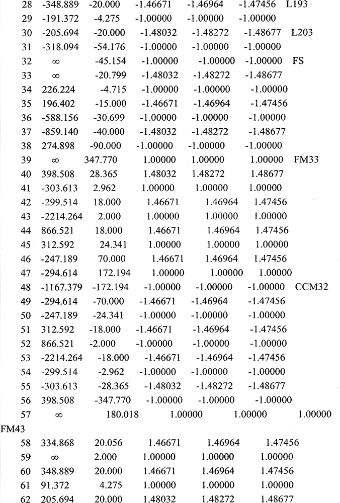

以下显示当各波长(g线、h线、i线)下的波面像差的rms值设为Wrms(g)、Wrms(h)、Wrms(i)时,各像高的值。 The following shows the value of each image height when the rms value of the wavefront aberration at each wavelength (g-line, h-line, i-line) is set to Wrms(g), Wrms(h), and Wrms(i). the
像高(mm) Wrms(g) Wrms(h) Wrms(i) Image height (mm) Wrms(g) Wrms(h) Wrms(i)
40.0 7.1mλ 5.6mλ 5.0mλ 40.0 7.1mλ 5.6mλ 5.0mλ
53.3 11.5mλ 3.3mλ 12.6mλ 53.3 11.5mλ 3.3mλ 12.6mλ
66.7 8.2mλ 4.5mλ 14.1mλ 66.7 8.2mλ 4.5mλ 14.1mλ
80.02 1.3mλ 24.7mλ 13.9mλ 80.02 1.3mλ 24.7mλ 13.9mλ
该实施例3的投影光学系统可对各波长下的波面像差进行良好的修正。 The projection optical system of the third embodiment can well correct the wavefront aberration at each wavelength. the
[产业上的可利用性] [Industrial availability]
本发明可适用于将光罩、光栅等的像投影于基板等上的投影光学系统、包括该投影光学系统的曝光装置、使用该曝光装置的曝光方法、使用该曝光装置的显示器的制造方法、光罩以及光罩的制造方法。 The present invention is applicable to a projection optical system for projecting an image of a mask, a grating, etc. on a substrate, etc., an exposure apparatus including the projection optical system, an exposure method using the exposure apparatus, a method of manufacturing a display using the exposure apparatus, A photomask and a method for manufacturing the photomask. the
Claims (6)
Applications Claiming Priority (4)
| Application Number | Priority Date | Filing Date | Title |
|---|---|---|---|
| JP2006-039446 | 2006-02-16 | ||
| JP2006039446 | 2006-02-16 | ||
| JP2007-014631 | 2007-01-25 | ||
| JP2007014631 | 2007-01-25 |
Related Parent Applications (1)
| Application Number | Title | Priority Date | Filing Date |
|---|---|---|---|
| CN2007800055642A Division CN101385123B (en) | 2006-02-16 | 2007-02-06 | Projection optical system, exposure apparatus and method, mask and method for manufacturing display |
Publications (2)
| Publication Number | Publication Date |
|---|---|
| CN101976018A CN101976018A (en) | 2011-02-16 |
| CN101976018B true CN101976018B (en) | 2013-01-30 |
Family
ID=38371384
Family Applications (2)
| Application Number | Title | Priority Date | Filing Date |
|---|---|---|---|
| CN2007800055642A Expired - Fee Related CN101385123B (en) | 2006-02-16 | 2007-02-06 | Projection optical system, exposure apparatus and method, mask and method for manufacturing display |
| CN2010105224975A Expired - Fee Related CN101976018B (en) | 2006-02-16 | 2007-02-06 | Photo-mask and manufacturing method thereof |
Family Applications Before (1)
| Application Number | Title | Priority Date | Filing Date |
|---|---|---|---|
| CN2007800055642A Expired - Fee Related CN101385123B (en) | 2006-02-16 | 2007-02-06 | Projection optical system, exposure apparatus and method, mask and method for manufacturing display |
Country Status (7)
| Country | Link |
|---|---|
| US (2) | US8305556B2 (en) |
| EP (1) | EP1986220A4 (en) |
| JP (2) | JP5453806B2 (en) |
| KR (1) | KR101415411B1 (en) |
| CN (2) | CN101385123B (en) |
| TW (1) | TWI424287B (en) |
| WO (1) | WO2007094198A1 (en) |
Families Citing this family (11)
| Publication number | Priority date | Publication date | Assignee | Title |
|---|---|---|---|---|
| US8208198B2 (en) * | 2004-01-14 | 2012-06-26 | Carl Zeiss Smt Gmbh | Catadioptric projection objective |
| US20080151365A1 (en) * | 2004-01-14 | 2008-06-26 | Carl Zeiss Smt Ag | Catadioptric projection objective |
| KR101391470B1 (en) | 2004-05-17 | 2014-05-07 | 칼 짜이스 에스엠티 게엠베하 | Catadioptric projection objective with intermediate images |
| US8917378B2 (en) | 2007-12-20 | 2014-12-23 | Nikon Corporation | Exposure method, exposure apparatus, and method for producing device with plurality of projection optical systems and pattern having first partial pattern area and second partial area having overlaid area with first partial pattern area |
| JP5392549B2 (en) * | 2009-05-12 | 2014-01-22 | 株式会社ニコン | Exposure method and apparatus, and device manufacturing method |
| KR102051842B1 (en) * | 2009-05-15 | 2019-12-04 | 가부시키가이샤 니콘 | Mobile apparatus, power transmission apparatus, exposure apparatus, and device manufacturing method |
| DE102009045217B3 (en) * | 2009-09-30 | 2011-04-07 | Carl Zeiss Smt Gmbh | Catadioptric projection lens |
| US8461556B2 (en) * | 2010-09-08 | 2013-06-11 | Varian Semiconductor Equipment Associates, Inc. | Using beam blockers to perform a patterned implant of a workpiece |
| CN103246158B (en) * | 2012-02-14 | 2015-03-25 | 旺宏电子股份有限公司 | Mask, its pattern arrangement method and exposure method |
| DE102017105580B4 (en) * | 2016-11-04 | 2025-10-02 | Carl Zeiss Meditec Ag | Surgical microscope |
| CN119036999B (en) * | 2024-07-25 | 2025-11-25 | 中国印钞造币集团有限公司 | Imaging methods, systems, electronic devices, and readable storage media for plate making and printing. |
Citations (5)
| Publication number | Priority date | Publication date | Assignee | Title |
|---|---|---|---|---|
| JPH08250399A (en) | 1995-03-14 | 1996-09-27 | Nikon Corp | Scanning exposure device |
| JPH11265848A (en) | 1997-12-20 | 1999-09-28 | Carl Zeiss:Fa | Projection aligner and exposure |
| EP1107064A2 (en) * | 1999-12-06 | 2001-06-13 | Olympus Optical Co., Ltd. | Exposure apparatus |
| CN1441461A (en) * | 2002-02-26 | 2003-09-10 | 株式会社东芝 | Mask base board and its producing method |
| JP2004335864A (en) * | 2003-05-09 | 2004-11-25 | Nikon Corp | Exposure apparatus and exposure method |
Family Cites Families (28)
| Publication number | Priority date | Publication date | Assignee | Title |
|---|---|---|---|---|
| JPS6442655A (en) * | 1987-08-11 | 1989-02-14 | Nec Corp | Structure of reticle |
| JPH05161588A (en) | 1991-12-16 | 1993-06-29 | Mitsubishi Electric Corp | Water level detector for dishwasher |
| US6157497A (en) * | 1993-06-30 | 2000-12-05 | Nikon Corporation | Exposure apparatus |
| US5729331A (en) * | 1993-06-30 | 1998-03-17 | Nikon Corporation | Exposure apparatus, optical projection apparatus and a method for adjusting the optical projection apparatus |
| JP3348467B2 (en) | 1993-06-30 | 2002-11-20 | 株式会社ニコン | Exposure apparatus and method |
| JPH0766113A (en) * | 1993-08-31 | 1995-03-10 | Sanyo Electric Co Ltd | Reticle and formation of verner for alignment thereof |
| JP3477838B2 (en) * | 1993-11-11 | 2003-12-10 | 株式会社ニコン | Scanning exposure apparatus and exposure method |
| JP4110606B2 (en) | 1998-02-12 | 2008-07-02 | 株式会社ニコン | Scanning exposure apparatus and exposure method |
| JP2000231184A (en) * | 1999-02-12 | 2000-08-22 | Toshiba Corp | Array substrate and manufacturing method thereof |
| JP2000331909A (en) * | 1999-05-19 | 2000-11-30 | Nikon Corp | Scanning exposure equipment |
| JP2001109169A (en) | 1999-10-13 | 2001-04-20 | Nikon Corp | Exposure apparatus, exposure method and mask |
| JP2001168003A (en) * | 1999-12-06 | 2001-06-22 | Olympus Optical Co Ltd | Aligner |
| KR100827874B1 (en) * | 2000-05-22 | 2008-05-07 | 가부시키가이샤 니콘 | Exposure apparatus, method for manufacturing thereof, method for exposing, method for manufacturing microdevice, and method for manufacturing device |
| TWI232348B (en) * | 2001-12-26 | 2005-05-11 | Pentax Corp | Projection aligner |
| US6898025B2 (en) * | 2002-06-04 | 2005-05-24 | Pentax Corporation | Projection aligner and optical system therefor |
| JP2004247487A (en) * | 2003-02-13 | 2004-09-02 | Canon Inc | Scanning exposure equipment |
| JP2004327660A (en) * | 2003-04-24 | 2004-11-18 | Nikon Corp | Scanning projection exposure apparatus, exposure method, and device manufacturing method |
| TWI282487B (en) * | 2003-05-23 | 2007-06-11 | Canon Kk | Projection optical system, exposure apparatus, and device manufacturing method |
| JP2005039211A (en) * | 2003-06-30 | 2005-02-10 | Canon Inc | Projection optical system, exposure apparatus, and device manufacturing method |
| JP2005024941A (en) * | 2003-07-03 | 2005-01-27 | Nikon Corp | Projection optical system, projection exposure apparatus, and projection exposure method |
| US6973375B2 (en) * | 2004-02-12 | 2005-12-06 | Mykrolis Corporation | System and method for flow monitoring and control |
| TWI271602B (en) * | 2004-03-31 | 2007-01-21 | Fujifilm Corp | A correcting method and an exposure method of exposure device, and an exposure device |
| KR101264936B1 (en) * | 2004-06-04 | 2013-05-15 | 가부시키가이샤 니콘 | Exposure apparatus exposure method and device producing method |
| JP4711437B2 (en) * | 2004-06-23 | 2011-06-29 | 株式会社ニコン | Projection optical system, exposure apparatus, and exposure method |
| JP2006039446A (en) | 2004-07-30 | 2006-02-09 | Ricoh Co Ltd | Image forming method, electrostatic image developing toner |
| JP2007014631A (en) | 2005-07-08 | 2007-01-25 | Sanyo Product Co Ltd | Game machine |
| JP4984810B2 (en) * | 2006-02-16 | 2012-07-25 | 株式会社ニコン | Exposure method, exposure apparatus, and photomask |
| JP5071382B2 (en) * | 2006-03-20 | 2012-11-14 | 株式会社ニコン | Scanning exposure apparatus and microdevice manufacturing method |
-
2007
- 2007-02-06 KR KR1020087013006A patent/KR101415411B1/en not_active Expired - Fee Related
- 2007-02-06 CN CN2007800055642A patent/CN101385123B/en not_active Expired - Fee Related
- 2007-02-06 EP EP07708092A patent/EP1986220A4/en not_active Withdrawn
- 2007-02-06 CN CN2010105224975A patent/CN101976018B/en not_active Expired - Fee Related
- 2007-02-06 WO PCT/JP2007/051974 patent/WO2007094198A1/en not_active Ceased
- 2007-02-06 JP JP2008500449A patent/JP5453806B2/en not_active Expired - Fee Related
- 2007-02-12 TW TW096105002A patent/TWI424287B/en not_active IP Right Cessation
-
2008
- 2008-08-12 US US12/190,260 patent/US8305556B2/en not_active Expired - Fee Related
-
2012
- 2012-09-26 US US13/627,526 patent/US8867019B2/en not_active Expired - Fee Related
-
2013
- 2013-04-08 JP JP2013080572A patent/JP2013178535A/en active Pending
Patent Citations (6)
| Publication number | Priority date | Publication date | Assignee | Title |
|---|---|---|---|---|
| JPH08250399A (en) | 1995-03-14 | 1996-09-27 | Nikon Corp | Scanning exposure device |
| US5715037A (en) * | 1995-03-14 | 1998-02-03 | Nikon Corporation | Scanning exposure apparatus |
| JPH11265848A (en) | 1997-12-20 | 1999-09-28 | Carl Zeiss:Fa | Projection aligner and exposure |
| EP1107064A2 (en) * | 1999-12-06 | 2001-06-13 | Olympus Optical Co., Ltd. | Exposure apparatus |
| CN1441461A (en) * | 2002-02-26 | 2003-09-10 | 株式会社东芝 | Mask base board and its producing method |
| JP2004335864A (en) * | 2003-05-09 | 2004-11-25 | Nikon Corp | Exposure apparatus and exposure method |
Also Published As
| Publication number | Publication date |
|---|---|
| EP1986220A4 (en) | 2010-08-18 |
| JP5453806B2 (en) | 2014-03-26 |
| WO2007094198A1 (en) | 2007-08-23 |
| US20130021589A1 (en) | 2013-01-24 |
| US20090021712A1 (en) | 2009-01-22 |
| KR101415411B1 (en) | 2014-07-04 |
| US8305556B2 (en) | 2012-11-06 |
| KR20080101867A (en) | 2008-11-21 |
| EP1986220A1 (en) | 2008-10-29 |
| TWI424287B (en) | 2014-01-21 |
| CN101385123A (en) | 2009-03-11 |
| JP2013178535A (en) | 2013-09-09 |
| HK1128061A1 (en) | 2009-10-16 |
| US8867019B2 (en) | 2014-10-21 |
| CN101385123B (en) | 2010-12-15 |
| JPWO2007094198A1 (en) | 2009-07-02 |
| CN101976018A (en) | 2011-02-16 |
| TW200732868A (en) | 2007-09-01 |
Similar Documents
| Publication | Publication Date | Title |
|---|---|---|
| CN101976018B (en) | Photo-mask and manufacturing method thereof | |
| KR100866818B1 (en) | Projection optical system and exposure apparatus comprising the same | |
| TWI443378B (en) | Reflection-refractive projection optical system, catadioptric optical device, scanning exposure device, and method of manufacturing micro-component | |
| KR102266723B1 (en) | Projection optical system, exposure apparatus, and article manufacturing method | |
| EP2003507A1 (en) | Scanning exposure apparatus, micro device manufacturing method, mask, projection optical apparatus and mask manufacturing method | |
| JP4779394B2 (en) | Projection optical system, exposure apparatus, and exposure method | |
| US8654307B2 (en) | Scanning type exposure apparatus, method of manufacturing micro-apparatus, mask, projection optical apparatus, and method of manufacturing mask | |
| KR20080106505A (en) | Projection optics, exposure apparatus, and device manufacturing method | |
| KR100522503B1 (en) | Projection optical system and projection exposure apparatus with the same, and device manufacturing method | |
| JP2003202494A (en) | Projection optical system, exposure apparatus, and device manufacturing method | |
| JP5360529B2 (en) | Projection optical system, exposure apparatus, and device manufacturing method | |
| HK1118382A (en) | Projection optical system, exposure device, exposure method, display manufacturing method, mask, and mask manufacturing method | |
| HK1128061B (en) | Projection optical system, exposure device and method, mask and display manufacturing method | |
| JP2004086110A (en) | Projection optical system, exposure apparatus and exposure method | |
| JP2004342711A (en) | Illumination optical device, exposure apparatus, and exposure method | |
| JP2009104184A (en) | Projection optical system, exposure apparatus, and device manufacturing method | |
| HK1123857A (en) | Reflective, refractive and projecting optical system; reflective, refractive and projecting device; scanning exposure device; and method of manufacturing micro device | |
| HK1124928A (en) | Scanning exposure apparatus, micro device manufacturing method, mask, projection optical apparatus and mask manufacturing method |
Legal Events
| Date | Code | Title | Description |
|---|---|---|---|
| C06 | Publication | ||
| PB01 | Publication | ||
| C10 | Entry into substantive examination | ||
| SE01 | Entry into force of request for substantive examination | ||
| C14 | Grant of patent or utility model | ||
| GR01 | Patent grant | ||
| CF01 | Termination of patent right due to non-payment of annual fee |
Granted publication date: 20130130 |