CN101964385B - Light emitting diode and making method thereof - Google Patents
Light emitting diode and making method thereof Download PDFInfo
- Publication number
- CN101964385B CN101964385B CN201010523853A CN201010523853A CN101964385B CN 101964385 B CN101964385 B CN 101964385B CN 201010523853 A CN201010523853 A CN 201010523853A CN 201010523853 A CN201010523853 A CN 201010523853A CN 101964385 B CN101964385 B CN 101964385B
- Authority
- CN
- China
- Prior art keywords
- layer
- emitting diode
- light
- bonding layer
- forming
- Prior art date
- Legal status (The legal status is an assumption and is not a legal conclusion. Google has not performed a legal analysis and makes no representation as to the accuracy of the status listed.)
- Expired - Fee Related
Links
Images


Classifications
-
- H—ELECTRICITY
- H10—SEMICONDUCTOR DEVICES; ELECTRIC SOLID-STATE DEVICES NOT OTHERWISE PROVIDED FOR
- H10H—INORGANIC LIGHT-EMITTING SEMICONDUCTOR DEVICES HAVING POTENTIAL BARRIERS
- H10H20/00—Individual inorganic light-emitting semiconductor devices having potential barriers, e.g. light-emitting diodes [LED]
- H10H20/80—Constructional details
- H10H20/83—Electrodes
- H10H20/831—Electrodes characterised by their shape
- H10H20/8314—Electrodes characterised by their shape extending at least partially onto an outer side surface of the bodies
-
- H—ELECTRICITY
- H10—SEMICONDUCTOR DEVICES; ELECTRIC SOLID-STATE DEVICES NOT OTHERWISE PROVIDED FOR
- H10H—INORGANIC LIGHT-EMITTING SEMICONDUCTOR DEVICES HAVING POTENTIAL BARRIERS
- H10H20/00—Individual inorganic light-emitting semiconductor devices having potential barriers, e.g. light-emitting diodes [LED]
- H10H20/01—Manufacture or treatment
- H10H20/011—Manufacture or treatment of bodies, e.g. forming semiconductor layers
- H10H20/018—Bonding of wafers
-
- H—ELECTRICITY
- H10—SEMICONDUCTOR DEVICES; ELECTRIC SOLID-STATE DEVICES NOT OTHERWISE PROVIDED FOR
- H10H—INORGANIC LIGHT-EMITTING SEMICONDUCTOR DEVICES HAVING POTENTIAL BARRIERS
- H10H20/00—Individual inorganic light-emitting semiconductor devices having potential barriers, e.g. light-emitting diodes [LED]
- H10H20/80—Constructional details
- H10H20/81—Bodies
- H10H20/815—Bodies having stress relaxation structures, e.g. buffer layers
-
- H—ELECTRICITY
- H10—SEMICONDUCTOR DEVICES; ELECTRIC SOLID-STATE DEVICES NOT OTHERWISE PROVIDED FOR
- H10H—INORGANIC LIGHT-EMITTING SEMICONDUCTOR DEVICES HAVING POTENTIAL BARRIERS
- H10H20/00—Individual inorganic light-emitting semiconductor devices having potential barriers, e.g. light-emitting diodes [LED]
- H10H20/80—Constructional details
- H10H20/85—Packages
- H10H20/857—Interconnections, e.g. lead-frames, bond wires or solder balls
-
- H—ELECTRICITY
- H10—SEMICONDUCTOR DEVICES; ELECTRIC SOLID-STATE DEVICES NOT OTHERWISE PROVIDED FOR
- H10H—INORGANIC LIGHT-EMITTING SEMICONDUCTOR DEVICES HAVING POTENTIAL BARRIERS
- H10H20/00—Individual inorganic light-emitting semiconductor devices having potential barriers, e.g. light-emitting diodes [LED]
- H10H20/80—Constructional details
- H10H20/85—Packages
- H10H20/858—Means for heat extraction or cooling
- H10H20/8581—Means for heat extraction or cooling characterised by their material
-
- H—ELECTRICITY
- H10—SEMICONDUCTOR DEVICES; ELECTRIC SOLID-STATE DEVICES NOT OTHERWISE PROVIDED FOR
- H10H—INORGANIC LIGHT-EMITTING SEMICONDUCTOR DEVICES HAVING POTENTIAL BARRIERS
- H10H20/00—Individual inorganic light-emitting semiconductor devices having potential barriers, e.g. light-emitting diodes [LED]
- H10H20/01—Manufacture or treatment
- H10H20/011—Manufacture or treatment of bodies, e.g. forming semiconductor layers
- H10H20/013—Manufacture or treatment of bodies, e.g. forming semiconductor layers having light-emitting regions comprising only Group III-V materials
- H10H20/0133—Manufacture or treatment of bodies, e.g. forming semiconductor layers having light-emitting regions comprising only Group III-V materials with a substrate not being Group III-V materials
- H10H20/01335—Manufacture or treatment of bodies, e.g. forming semiconductor layers having light-emitting regions comprising only Group III-V materials with a substrate not being Group III-V materials the light-emitting regions comprising nitride materials
-
- H10P90/1914—
Landscapes
- Led Devices (AREA)
Abstract
一种发光二极管及其形成方法,所述发光二极管的形成方法包括:分别提供半导体基底和蓝宝石基底,所述半导体基底上形成有第一键合层,所述蓝宝石基底上依次形成有牺牲层、发光二极管管芯和第二键合层;将所述第一键合层和第二键合层键合;去除所述牺牲层,将所述蓝宝石基底剥离。本发明增大了发光二极管的有效发光面积,改善了散热,提高了发光效率。
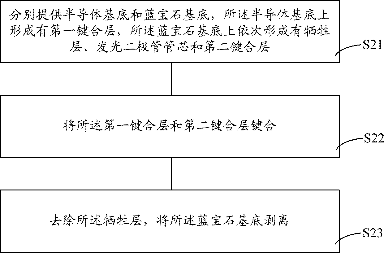
A light-emitting diode and its forming method, the forming method of the light-emitting diode comprising: respectively providing a semiconductor substrate and a sapphire substrate, a first bonding layer is formed on the semiconductor substrate, a sacrificial layer, The light-emitting diode tube core and the second bonding layer; bonding the first bonding layer and the second bonding layer; removing the sacrificial layer, and peeling off the sapphire substrate. The invention increases the effective light-emitting area of the light-emitting diode, improves heat dissipation and improves light-emitting efficiency.
Description
技术领域 technical field
本发明涉及半导体照明领域,尤其涉及一种发光二极管及其形成方法。The invention relates to the field of semiconductor lighting, in particular to a light emitting diode and a forming method thereof.
背景技术 Background technique
半导体发光二极管(LED,Light Emitting Diode)是一种半导体固体发光器件,主要是利用固体半导体芯片作为发光材料,在半导体中通过载流子发生复合放出过剩的能量而引起光子发射,直接发出红、黄、蓝、绿、青、橙、紫等色的光。Semiconductor light-emitting diode (LED, Light Emitting Diode) is a semiconductor solid-state light-emitting device, which mainly uses a solid semiconductor chip as a light-emitting material. In the semiconductor, the excess energy is released through the recombination of carriers in the semiconductor to cause photon emission, directly emitting red, Yellow, blue, green, blue, orange, purple and other colors of light.
发光二极管根据发光颜色的不同,分为单色发光二极管和白光发光二极管。二十世纪八十年代出现了超高亮度红色发光二极管,早期的红色发光二极管的衬底为不透明材料,发光效率为1-2lumens/watt(流明/瓦);之后对其进行了改进,采用透明的衬底;在所有的超高亮度红色发光二极管中,最好的模型的效率约为9lumens/watt(流明/瓦),光谱范围通常在650nm-640nm,驱动电流值通常在30mA-50mA,在1.5V电压时发光灰暗。随后开发了在GaP(磷化镓)衬底上形成的高效率红色发光二极管、橙红色发光二极管以及橙色发光二极管;之后又开发了超亮度橙红色发光二极管、橙色发光二极管、黄色发光二极管。第一个绿色发光二极管由GaP(磷化镓)形成,其效率为每瓦数十流明,最大驱动电流通常为30mA;随后出现了高效率绿色发光二极管,之后出现了绿色发光二极管。第一个超亮度宽波带GaN蓝色发光二极管在20世纪90年代由Nichia开发成功,光谱范围跨越紫色、蓝色和绿色区域,波峰宽度为450nm。第一个超亮度SiC蓝色发光二极管在20世纪90年代由Cree开发成功,光谱范围非常宽,尤其在淡蓝色(mid-blue)到紫色光谱范围内强度很强,波峰范围在428-430nm,最大驱动电流约为30mA,通常使用10mA。Light-emitting diodes are divided into monochromatic light-emitting diodes and white light-emitting diodes according to the different light-emitting colors. In the 1980s, ultra-high-brightness red light-emitting diodes appeared. The substrates of early red light-emitting diodes were opaque materials, and the luminous efficiency was 1-2lumens/watt (lumens/watt); In all ultra-high brightness red light-emitting diodes, the efficiency of the best model is about 9lumens/watt (lumen/watt), the spectral range is usually 650nm-640nm, and the driving current value is usually 30mA-50mA. When the voltage is 1.5V, the light is dim. Subsequently, high-efficiency red light-emitting diodes, orange-red light-emitting diodes, and orange light-emitting diodes formed on GaP (gallium phosphide) substrates were developed; and then ultra-brightness orange-red light-emitting diodes, orange light-emitting diodes, and yellow light-emitting diodes were developed. The first green LEDs were formed from GaP (gallium phosphide), which had an efficiency of tens of lumens per watt and a maximum drive current of typically 30mA; high-efficiency green LEDs followed, and green LEDs followed. The first ultra-brightness broadband GaN blue light-emitting diode was successfully developed by Nichia in the 1990s, with a spectral range spanning the violet, blue and green regions, and a peak width of 450nm. The first ultra-brightness SiC blue light-emitting diode was successfully developed by Cree in the 1990s. It has a very wide spectral range, especially in the light blue (mid-blue) to purple spectral range. The intensity is very strong, and the peak range is 428-430nm. , the maximum drive current is about 30mA, usually 10mA is used.
图1为现有技术的单色发光二极管结构的示意图,以蓝色发光二极管为例,参考图1,现有技术中的单色发光二极管的结构一般为在蓝宝石基底(Al2O3)10上形成材料为N型掺杂的氮化镓(n-GaN)的缓冲层11,在缓冲层11上形成材料为氮化镓铟(InGaN)的多量子阱有源层12,在多量子阱有源层12上形成材料为P型掺杂的氮化镓(p-GaN)的帽层13,其中,缓冲层11、多量子阱有源层12和帽层13共同构成了发光二极管管芯,此外帽层13上还形成有透明的金属接触层14。正电极15与所述帽层13电连接,为了将缓冲层11引出,在所述金属接触层14、帽层13、多量子阱有源层12和缓冲层11上形成凹槽16,在凹槽16的底部形成负电极17,所述负电极17与缓冲层11电连接,从而可以通过正电极15和负电极17向所述发光二极管管芯施加电压,使发光二极管发光。Fig. 1 is a schematic diagram of the structure of a monochromatic light-emitting diode in the prior art. Taking a blue light-emitting diode as an example, referring to Fig. 1, the structure of a monochromatic light-emitting diode in the prior art is generally on a sapphire substrate (Al 2 O 3 ) 10 A buffer layer 11 of N-type doped gallium nitride (n-GaN) is formed on the buffer layer 11, and a multi-quantum well active layer 12 whose material is indium gallium nitride (InGaN) is formed on the buffer layer 11. In the multi-quantum well On the active layer 12, a cap layer 13 made of p-type doped gallium nitride (p-GaN) is formed, wherein the buffer layer 11, the multi-quantum well active layer 12 and the cap layer 13 together constitute a light emitting diode die , in addition, a transparent metal contact layer 14 is formed on the cap layer 13 . Positive electrode 15 is electrically connected with described cap layer 13, in order to draw out buffer layer 11, form groove 16 on described metal contact layer 14, cap layer 13, MQW active layer 12 and buffer layer 11, in concave A negative electrode 17 is formed at the bottom of the groove 16, and the negative electrode 17 is electrically connected to the buffer layer 11, so that a voltage can be applied to the LED core through the positive electrode 15 and the negative electrode 17, so that the LED emits light.
现有技术的发光二极管结构多采用蓝宝石基底10,由于该材质为绝缘体,因此需要形成凹槽16,并通过负电极17将缓冲层11引出,凹槽16导致有效的发光面积减小。The light-emitting diode structure in the prior art mostly uses the sapphire substrate 10. Since the material is an insulator, a groove 16 needs to be formed, and the buffer layer 11 is led out through the negative electrode 17. The groove 16 reduces the effective light-emitting area.
发明内容 Contents of the invention
本发明解决的问题是提供一种发光二极管及其形成方法,增大发光二极管的有效发光面积。The problem to be solved by the present invention is to provide a light-emitting diode and its forming method, which can increase the effective light-emitting area of the light-emitting diode.
为解决上述问题,本发明提供一种发光二极管的形成方法,包括:In order to solve the above problems, the present invention provides a method for forming a light emitting diode, comprising:
分别提供半导体基底和蓝宝石基底,所述半导体基底上形成有第一键合层,所述蓝宝石基底上依次形成有牺牲层、发光二极管管芯和第二键合层;A semiconductor substrate and a sapphire substrate are respectively provided, a first bonding layer is formed on the semiconductor substrate, a sacrificial layer, a light-emitting diode die and a second bonding layer are sequentially formed on the sapphire substrate;
将所述第一键合层和第二键合层键合;bonding the first bonding layer and the second bonding layer;
去除所述牺牲层,将所述蓝宝石基底剥离。The sacrificial layer is removed, and the sapphire substrate is peeled off.
可选的,所述发光二极管的形成方法还包括:在剥离蓝宝石基底后暴露出的发光二极管管芯的表面形成连接电极。Optionally, the method for forming the light emitting diode further includes: forming connection electrodes on the exposed surface of the light emitting diode die after peeling off the sapphire substrate.
可选的,所述牺牲层的厚度为10nm至50nm。Optionally, the sacrificial layer has a thickness of 10 nm to 50 nm.
可选的,所述牺牲层的材料为磷化硼。Optionally, the material of the sacrificial layer is boron phosphide.
可选的,所述去除所述牺牲层包括:使用氯化氢气体刻蚀去除所述牺牲层。Optionally, the removing the sacrificial layer includes: using hydrogen chloride gas to etch and remove the sacrificial layer.
可选的,在所述蓝宝石基底和牺牲层之间还形成有缓冲层。Optionally, a buffer layer is also formed between the sapphire substrate and the sacrificial layer.
可选的,所述缓冲层的材料为氮化铝。Optionally, the material of the buffer layer is aluminum nitride.
可选的,所述第一键合层的材料为钯,所述第二键合层的材料为铟或银。Optionally, the material of the first bonding layer is palladium, and the material of the second bonding layer is indium or silver.
可选的,所述第一键合层的材料为钯,所述第二键合层为铟和钯的叠层结构,或银和钯的叠层结构。Optionally, the material of the first bonding layer is palladium, and the second bonding layer is a stacked structure of indium and palladium, or a stacked structure of silver and palladium.
可选的,所述第一键合层的材料为钯,所述第二键合层为铟的单层结构或铟和钯的叠层结构,所述键合的反应温度为180℃至220℃。Optionally, the material of the first bonding layer is palladium, the second bonding layer is a single-layer structure of indium or a stacked structure of indium and palladium, and the reaction temperature of the bonding is 180°C to 220°C. ℃.
可选的,所述第二键合层和发光二极管管芯之间还形成有接触电极层。Optionally, a contact electrode layer is further formed between the second bonding layer and the LED die.
可选的,所述接触电极层的材料为钛。Optionally, the material of the contact electrode layer is titanium.
可选的,所述接触电极层的厚度为2nm至10nm。Optionally, the contact electrode layer has a thickness of 2 nm to 10 nm.
可选的,所述发光二极管管芯包括依次位于所述牺牲层上的帽层、有源层和缓冲层。Optionally, the LED die includes a cap layer, an active layer and a buffer layer sequentially located on the sacrificial layer.
可选的,所述半导体基底为N型掺杂的硅衬底。Optionally, the semiconductor substrate is an N-type doped silicon substrate.
为解决上述问题,本发明提供了一种发光二极管,包括:In order to solve the above problems, the present invention provides a light emitting diode, comprising:
半导体基底;semiconductor substrate;
键合层,形成于所述半导体基底的表面上;a bonding layer formed on the surface of the semiconductor substrate;
发光二极管管芯,形成于所述键合层的表面上。The LED chip is formed on the surface of the bonding layer.
可选的,所述发光二极管管芯的表面上还形成有连接电极。Optionally, connection electrodes are also formed on the surface of the light emitting diode die.
可选的,所述键合层的材料为铟化钯或银化钯。Optionally, the material of the bonding layer is palladium indium or palladium silver.
可选的,还包括接触电极层,形成于所述键合层和发光二极管管芯之间。Optionally, a contact electrode layer is also included, formed between the bonding layer and the LED die.
可选的,所述接触电极层的材料为钛。Optionally, the material of the contact electrode layer is titanium.
可选的,所述接触电极层的厚度为2nm至10nm。Optionally, the contact electrode layer has a thickness of 2 nm to 10 nm.
可选的,所述发光二极管管芯包括依次位于所述键合层上的缓冲层、有源层和帽层。Optionally, the LED die includes a buffer layer, an active layer and a cap layer sequentially located on the bonding layer.
可选的,所述半导体基底为N型掺杂的硅衬底。Optionally, the semiconductor substrate is an N-type doped silicon substrate.
与现有技术相比,本发明具有以下优点:Compared with the prior art, the present invention has the following advantages:
本技术方案的发光二极管的形成方法中,分别提供半导体基底和蓝宝石基底,所述半导体基底上形成有第一键合层,所述蓝宝石基底上依次形成有牺牲层、发光二极管管芯和第二键合层,之后将所述第一键合层和第二键合层键合,并去除所述牺牲层,将所述蓝宝石基底剥离,从而将所述发光二极管管芯转移至所述半导体基底上,由于所述半导体基底具有良好的导电性,可以直接将所述发光二极管管芯的一极引出,并不需要形成凹槽,从而增大了有效的发光面积。In the method for forming a light-emitting diode according to the technical solution, a semiconductor substrate and a sapphire substrate are respectively provided, a first bonding layer is formed on the semiconductor substrate, a sacrificial layer, a light-emitting diode die, and a second bonding layer are sequentially formed on the sapphire substrate. bonding layer, then bonding the first bonding layer and the second bonding layer, removing the sacrificial layer, peeling off the sapphire substrate, thereby transferring the light emitting diode die to the semiconductor substrate In addition, since the semiconductor substrate has good conductivity, one pole of the light-emitting diode die can be directly drawn out without forming a groove, thereby increasing the effective light-emitting area.
此外,半导体基底较蓝宝石基底具有更好的导热性,将发光二极管管芯转移至半导体基底上,有助于发光过程中的散热,提高发光效率。In addition, the semiconductor substrate has better thermal conductivity than the sapphire substrate, and transferring the light-emitting diode die to the semiconductor substrate helps heat dissipation during the light-emitting process and improves luminous efficiency.
附图说明 Description of drawings
图1是现有技术的发光二极管的剖面结构示意图;Fig. 1 is a schematic cross-sectional structure diagram of a light emitting diode in the prior art;
图2是本发明实施例的发光二极管的形成方法的流程示意图;2 is a schematic flow chart of a method for forming a light emitting diode according to an embodiment of the present invention;
图3至图6是本发明实施例的发光二极管的形成方法对应的中间结构的剖面结构示意图。3 to 6 are cross-sectional schematic diagrams of intermediate structures corresponding to the method for forming a light emitting diode according to an embodiment of the present invention.
具体实施方式 Detailed ways
现有技术的发光二极管中,一般将发光二极管管芯形成在蓝宝石基底上,由于蓝宝石基底为绝缘材料,因此需要在发光二极管管芯上形成凹槽,以形成连接电极,导致有效的发光面积降低。In the light-emitting diodes of the prior art, the light-emitting diode die is generally formed on the sapphire substrate. Since the sapphire substrate is an insulating material, it is necessary to form grooves on the light-emitting diode die to form the connecting electrodes, resulting in a decrease in the effective light-emitting area. .
本技术方案的发光二极管的形成方法中,分别提供半导体基底和蓝宝石基底,所述半导体基底上形成有第一键合层,所述蓝宝石基底上依次形成有牺牲层、发光二极管管芯和第二键合层,之后将所述第一键合层和第二键合层键合,并去除所述牺牲层,将所述蓝宝石基底剥离,从而将所述发光二极管管芯转移至所述半导体基底上,由于所述半导体基底具有良好的导电性,可以直接将所述发光二极管管芯的一极引出,并不需要形成凹槽,从而增大了有效的发光面积。In the method for forming a light-emitting diode according to the technical solution, a semiconductor substrate and a sapphire substrate are respectively provided, a first bonding layer is formed on the semiconductor substrate, a sacrificial layer, a light-emitting diode die, and a second bonding layer are sequentially formed on the sapphire substrate. bonding layer, then bonding the first bonding layer and the second bonding layer, removing the sacrificial layer, peeling off the sapphire substrate, thereby transferring the light emitting diode die to the semiconductor substrate In addition, since the semiconductor substrate has good conductivity, one pole of the light-emitting diode die can be directly drawn out without forming a groove, thereby increasing the effective light-emitting area.
此外,半导体基底较蓝宝石基底具有更好的导热性,将发光二极管管芯转移至半导体基底上,有助于发光过程中的散热,提高发光效率。In addition, the semiconductor substrate has better thermal conductivity than the sapphire substrate, and transferring the light-emitting diode die to the semiconductor substrate helps heat dissipation during the light-emitting process and improves luminous efficiency.
为了使本领域技术人员可以更好的理解本发明的精神,下面结合附图详细说明本发明的具体实施例。In order to enable those skilled in the art to better understand the spirit of the present invention, specific embodiments of the present invention will be described in detail below in conjunction with the accompanying drawings.
在以下描述中阐述了具体细节以便于充分理解本发明。但是本发明能够以多种不同于在此描述的其它方式来实施,本领域技术人员可以在不违背本发明内涵的情况下做类似推广。因此本发明不受下面公开的具体实施方式的限制。In the following description, specific details are set forth in order to provide a thorough understanding of the present invention. However, the present invention can be implemented in many other ways than those described here, and those skilled in the art can make similar extensions without departing from the connotation of the present invention. Accordingly, the present invention is not limited to the specific embodiments disclosed below.
图2为本发明实施例的发光二极管的形成方法的流程示意图,包括:2 is a schematic flow chart of a method for forming a light emitting diode according to an embodiment of the present invention, including:
步骤S21,分别提供半导体基底和蓝宝石基底,所述半导体基底上形成有第一键合层,所述蓝宝石基底上依次形成有牺牲层、发光二极管管芯和第二键合层;Step S21, providing a semiconductor substrate and a sapphire substrate respectively, a first bonding layer is formed on the semiconductor substrate, a sacrificial layer, a light emitting diode die and a second bonding layer are sequentially formed on the sapphire substrate;
步骤S22,将所述第一键合层和第二键合层键合;Step S22, bonding the first bonding layer and the second bonding layer;
步骤S23,去除所述牺牲层,将所述蓝宝石基底剥离。Step S23 , removing the sacrificial layer, and peeling off the sapphire substrate.
下面结合图2和图3至图6对本发明实施例的发光二极管的形成方法进行详细说明。The method for forming the light emitting diode according to the embodiment of the present invention will be described in detail below with reference to FIG. 2 and FIG. 3 to FIG. 6 .
结合图2和图3,执行步骤S21,分别提供半导体基底和蓝宝石基底,所述半导体基底上形成有第一键合层,所述蓝宝石基底上依次形成有牺牲层、发光二极管管芯和第二键合层。2 and 3, step S21 is performed to provide a semiconductor substrate and a sapphire substrate respectively. A first bonding layer is formed on the semiconductor substrate, and a sacrificial layer, a light-emitting diode die, and a second bonding layer are sequentially formed on the sapphire substrate. bonding layer.
具体的,提供半导体基底20,所述半导体基底20的表面上形成有第一键合层21。所述半导体基底20的材质为半导体材料,可以是单晶硅,也可以是也可以是硅、锗、砷化镓或硅锗化合物,本实施例中具体为N型掺杂的硅衬底,其电阻率为0.01至0.1Ω·cm,所述第一键合层21的材料为钯(Pd)。在一具体实施例中,可以在所述半导体基底20的表面通过物理气相沉积(PVD)形成钯材料的第一键合层21。所述第一键合层21的厚度范围为80nm至120nm,本实施例中优选为100nm。Specifically, a
提供蓝宝石基底30,所述蓝宝石基底30的材料主要为Al2O3,其表面上依次形成有缓冲层31、牺牲层32、发光二极管管芯33、接触电极层34和第二键合层35。所述缓冲层31用于蓝宝石基底30和牺牲层32之间的应力缓冲和晶格匹配,改善二者的粘附性。本实施例中,所述牺牲层32的材料为磷化硼(BP),其形成方法为金属有机物化学气相沉积(MOCVD),其厚度为10nm至50nm;所述缓冲层31的材料为氮化铝(AlN),其形成方法为金属有机物化学气相沉积,其厚度为100nm至5000nm。A
所述发光二极管管芯33包括依次形成在所述牺牲层32之上的帽层33c、有源层33b和缓冲层33a。所述帽层33c的材料为p-GaN;所述有源层33b为多量子阱有源层,其材料为InGaN,当然在其他实施例中,也可为单量子阱有源层以及本领域技术人员公知的其他有源层;所述缓冲层33a的材料为n-GaN。所述帽层33c、有源层33b和缓冲层33a的形成方法都为金属有机物化学气相沉积。The LED die 33 includes a
所述接触电极层34的材料为钛(Ti),其形成方法为物理气相沉积,其厚度为2nm至10nm,本实施例中优选为5nm。所述接触电极层34主要用于降低第二键合层35与发光二极管管芯33之间的接触电阻,改善电接触。The
所述第二键合层35可以为铟(In)或银(Ag)的单层结构,或是铟和钯的叠层结构,或是银和钯的叠层结构,本实施例中,所述第二键合层35为叠层结构,包括依次形成在所述接触电极层34之上的钯薄膜35b和铟薄膜35a。所述第二键合层35的形成方法为物理气相沉积,其中,所述钯薄膜35b的厚度为80nm至120nm,本实施例中优选为100nm,所述铟薄膜35a的厚度为0.8μm至1.2μm,本实施例中优选为1μm。The second bonding layer 35 can be a single-layer structure of indium (In) or silver (Ag), or a stacked structure of indium and palladium, or a stacked structure of silver and palladium. In this embodiment, the The second bonding layer 35 is a laminated structure, including a palladium
需要说明的是,所述缓冲层32和接触电极层34是可选的,在其他实施例中,可以仅形成其中的一个或是二者都不形成,如所述牺牲层32直接形成在蓝宝石基底30上,所述第二键合层35直接形成在所述发光二极管管芯33上。It should be noted that the
结合图2和图4,执行步骤S22,将所述第一键合层和第二键合层键合。具体的,将所述第一键合层21和第二键合层35键合,使得第一键合层21和第二键合层35反应形成键合层36。本实施例中,第一键合层21的材料为钯,第二键合层35包括铟薄膜35a和钯薄膜35b,键合反应后生成的键合层36的材料为铟化钯(BdIn3)。所述键合的反应温度为180℃至220℃,优选为200℃。在键合过程中,还可以通入氮气或其他非活泼气体的等离子体,以降低键合反应的温度,提高键合速度。此外,所述第二键合层35还可以为铟的单层结构,相应键合的反应温度为180℃至220℃,类似的,也可以通入氮气或其他非活泼气体的等离子体,以降低键合反应的温度。Referring to FIG. 2 and FIG. 4 , step S22 is performed to bond the first bonding layer and the second bonding layer. Specifically, the
由于所述第二键合层35为叠层结构,包括铟薄膜35a和钯薄膜35b,因此在键合过程中,铟薄膜35a夹于钯薄膜35b和钯材料的第一键合层21之间,使得铟薄膜35a能够同时与钯薄膜35b和第一键合层21中的钯材料发生反应,进一步加快了键合的反应速率。Since the second bonding layer 35 is a laminated structure, including an indium film 35a and a
在其他实施例中,所述第二键合层35的材料可以为银的单层结构或者银和钯的叠层结构,键合后形成的键合层36的材料为银化钯,键合过程的反应温度要高于铟与钯的键合温度。In other embodiments, the material of the second bonding layer 35 can be a single-layer structure of silver or a laminated structure of silver and palladium, and the material of the
结合图2和图5,执行步骤S23,去除所述牺牲层,将所述蓝宝石基底剥离。具体的,去除所述牺牲层32,将蓝宝石基底30以及其上的缓冲层31与所述发光二极管管芯33剥离。本实施例中,所述牺牲层32的材料为磷化硼,去除的过程主要使用氯化氢(HCl)气体刻蚀,刻蚀的过程具有选择性,仅会去除所述牺牲层32,而不会对其他膜层造成影响。Referring to FIG. 2 and FIG. 5 , step S23 is performed to remove the sacrificial layer and peel off the sapphire substrate. Specifically, the
至此,通过键合和剥离过程,使得所述发光二极管管芯33从蓝宝石基底30上转移至了半导体基底20上。所述发光二极管管芯33的一端通过所述接触电极层34、键合层36和半导体基底20电连接,半导体基底20作为发光二极管的负电极,可以连接负电压;所述发光二极管管芯33的另一端暴露出来,可以直接施加正电压,使所述发光二极管管芯33发光,而不需要专门形成沟槽来制作电极,从而增大了有效的发光面积。此外,由于半导体基底20的导热性大大优于蓝宝石基底30的导热性,因此,在发光二极管管芯33发光过程中产生的热量可以及时通过半导体基底20散播出去,避免过热导致的发光效率下降的问题,有利于提高整个发光二极管的发光效率。So far, the LED die 33 has been transferred from the
至此,本实施例形成的发光二极管的结构包括:半导体基底20;键合层36,形成于所述半导体基底20的表面上;接触电极层34,形成在所述键合层36的表面上;发光二极管管芯33,形成在所述接触电极层34的表面上。其中,所述接触电极层34为可选的,即所述发光二极管管芯33可以直接形成在所述键合层36的表面上。So far, the structure of the light emitting diode formed in this embodiment includes: a
参考图6,在刻蚀剥离之后,本实施例还在剥离蓝宝石基底后发光二极管管芯33暴露出的表面上形成连接电极37,作为正电极。所述连接电极37的材料为金(Au)或镍(Ni),或是本领域技术人员公知的其他材料。此外,还可以将所述半导体基底20固定在互连基板38上,所述互连基板38的材料为铝或其他导电金属,使得半导体基底20和所述互连基板38电连接。在实际应用中,可以将多个发光二极管以及相应的外围电路共同连接在所述互连基板38上,以形成发光阵列。Referring to FIG. 6 , after the etching and stripping, in this embodiment, a connecting
至此,在图5的基础上,本实施例形成的发光二极管的结构还包括位于发光二极管管芯33上的连接电极37,以及与所述半导体基底20电连接的互连基板38。So far, on the basis of FIG. 5 , the structure of the light emitting diode formed in this embodiment further includes the
本发明虽然已以较佳实施例公开如上,但其并不是用来限定本发明,任何本领域技术人员在不脱离本发明的精神和范围内,都可以利用上述揭示的方法和技术内容对本发明技术方案做出可能的变动和修改,因此,凡是未脱离本发明技术方案的内容,依据本发明的技术实质对以上实施例所作的任何简单修改、等同变化及修饰,均属于本发明技术方案的保护范围。Although the present invention has been disclosed as above with preferred embodiments, it is not intended to limit the present invention, and any person skilled in the art can use the methods disclosed above and technical content to analyze the present invention without departing from the spirit and scope of the present invention. Possible changes and modifications are made in the technical solution. Therefore, any simple modification, equivalent change and modification made to the above embodiments according to the technical essence of the present invention, which do not depart from the content of the technical solution of the present invention, all belong to the technical solution of the present invention. protected range.
Claims (11)
Priority Applications (5)
| Application Number | Priority Date | Filing Date | Title |
|---|---|---|---|
| CN201010523853A CN101964385B (en) | 2010-10-28 | 2010-10-28 | Light emitting diode and making method thereof |
| EP11835460.4A EP2637221B1 (en) | 2010-10-28 | 2011-02-10 | Light emitting diode and forming method thereof |
| US13/881,723 US8969108B2 (en) | 2010-10-28 | 2011-02-10 | Light emitting diode and forming method thereof |
| PCT/CN2011/070901 WO2012055186A1 (en) | 2010-10-28 | 2011-02-10 | Light emitting diode and forming method thereof |
| US14/592,396 US9202985B2 (en) | 2010-10-28 | 2015-01-08 | Light emitting diode and forming method thereof |
Applications Claiming Priority (1)
| Application Number | Priority Date | Filing Date | Title |
|---|---|---|---|
| CN201010523853A CN101964385B (en) | 2010-10-28 | 2010-10-28 | Light emitting diode and making method thereof |
Publications (2)
| Publication Number | Publication Date |
|---|---|
| CN101964385A CN101964385A (en) | 2011-02-02 |
| CN101964385B true CN101964385B (en) | 2012-08-29 |
Family
ID=43517198
Family Applications (1)
| Application Number | Title | Priority Date | Filing Date |
|---|---|---|---|
| CN201010523853A Expired - Fee Related CN101964385B (en) | 2010-10-28 | 2010-10-28 | Light emitting diode and making method thereof |
Country Status (4)
| Country | Link |
|---|---|
| US (2) | US8969108B2 (en) |
| EP (1) | EP2637221B1 (en) |
| CN (1) | CN101964385B (en) |
| WO (1) | WO2012055186A1 (en) |
Families Citing this family (12)
| Publication number | Priority date | Publication date | Assignee | Title |
|---|---|---|---|---|
| CN101964385B (en) | 2010-10-28 | 2012-08-29 | 映瑞光电科技(上海)有限公司 | Light emitting diode and making method thereof |
| CN102903804B (en) * | 2011-07-25 | 2015-12-16 | 财团法人工业技术研究院 | Light-emitting element transfer method and light-emitting element array |
| US9306117B2 (en) | 2011-07-25 | 2016-04-05 | Industrial Technology Research Institute | Transfer-bonding method for light emitting devices |
| CN102569331B (en) * | 2011-12-09 | 2014-04-16 | 北京工业大学 | Negative feedback longitudinal integration white light-emitting diode without phosphor powder |
| CN103682020A (en) * | 2012-08-31 | 2014-03-26 | 展晶科技(深圳)有限公司 | Manufacture method for LED (Light emitting diode) grain |
| CN103996755B (en) * | 2014-05-21 | 2016-08-17 | 天津三安光电有限公司 | A kind of preparation method of iii-nitride light emitting devices assembly |
| CN104810444B (en) * | 2015-03-04 | 2018-01-09 | 华灿光电(苏州)有限公司 | LED epitaxial slice and preparation method thereof, light-emitting diode chip for backlight unit prepares and substrate recovery method |
| CN104993031B (en) * | 2015-06-12 | 2018-03-06 | 映瑞光电科技(上海)有限公司 | High pressure flip LED chips and its manufacture method |
| US9444019B1 (en) * | 2015-09-21 | 2016-09-13 | Epistar Corporation | Method for reusing a substrate for making light-emitting device |
| US10957818B2 (en) * | 2016-09-30 | 2021-03-23 | Intel Corporation | High performance light emitting diode and monolithic multi-color pixel |
| CN112968095A (en) * | 2020-11-18 | 2021-06-15 | 重庆康佳光电技术研究院有限公司 | Light emitting diode chip and preparation method thereof |
| CN114497322A (en) * | 2022-03-31 | 2022-05-13 | 江西兆驰半导体有限公司 | A method of fabricating a flip-chip structure |
Family Cites Families (19)
| Publication number | Priority date | Publication date | Assignee | Title |
|---|---|---|---|---|
| US20010042866A1 (en) * | 1999-02-05 | 2001-11-22 | Carrie Carter Coman | Inxalygazn optical emitters fabricated via substrate removal |
| TWI226139B (en) * | 2002-01-31 | 2005-01-01 | Osram Opto Semiconductors Gmbh | Method to manufacture a semiconductor-component |
| KR100483049B1 (en) * | 2003-06-03 | 2005-04-15 | 삼성전기주식회사 | A METHOD OF PRODUCING VERTICAL GaN LIGHT EMITTING DIODES |
| JP2006073619A (en) * | 2004-08-31 | 2006-03-16 | Sharp Corp | Nitride compound semiconductor light emitting device |
| US8101498B2 (en) * | 2005-04-21 | 2012-01-24 | Pinnington Thomas Henry | Bonded intermediate substrate and method of making same |
| US7273798B2 (en) | 2005-08-01 | 2007-09-25 | Avago Technologies Ecbu Ip (Singapore) Pte. Ltd. | Gallium nitride device substrate containing a lattice parameter altering element |
| US10873002B2 (en) * | 2006-10-20 | 2020-12-22 | Cree, Inc. | Permanent wafer bonding using metal alloy preform discs |
| CN101536202A (en) * | 2006-11-17 | 2009-09-16 | 3M创新有限公司 | High efficiency light emitting articles and methods of forming the same |
| EP2087533A2 (en) * | 2006-11-17 | 2009-08-12 | 3M Innovative Properties Company | Planarized led with optical extractor |
| US7795054B2 (en) * | 2006-12-08 | 2010-09-14 | Samsung Led Co., Ltd. | Vertical structure LED device and method of manufacturing the same |
| CN101005110A (en) * | 2007-01-12 | 2007-07-25 | 中国科学院上海微系统与信息技术研究所 | Method for realizing gallium nitride ELD vertical structure using metal bounding process |
| KR100765453B1 (en) * | 2007-03-20 | 2007-10-09 | (주)에피플러스 | Formation method of light emitting diode |
| JP2008263126A (en) * | 2007-04-13 | 2008-10-30 | Oki Data Corp | Semiconductor device, method for manufacturing semiconductor device, LED head, and image forming apparatus |
| JP2009099675A (en) * | 2007-10-15 | 2009-05-07 | Showa Denko Kk | Light emitting diode manufacturing method, light emitting diode, and lamp |
| US20090280588A1 (en) * | 2008-05-06 | 2009-11-12 | Leo Mathew | Method of forming an electronic device including removing a differential etch layer |
| JP2010219377A (en) * | 2009-03-18 | 2010-09-30 | Toshiba Corp | Semiconductor light-emitting device and method of manufacturing the same |
| CN101872813A (en) * | 2009-04-24 | 2010-10-27 | 刘胜 | Light-emitting diode chip and manufacturing method thereof |
| CN101599523A (en) * | 2009-06-01 | 2009-12-09 | 广东昭信光电科技有限公司 | The light emitting diode (LED) chip with vertical structure and the manufacture method thereof that adopt conducting polymer to shift |
| CN101964385B (en) | 2010-10-28 | 2012-08-29 | 映瑞光电科技(上海)有限公司 | Light emitting diode and making method thereof |
-
2010
- 2010-10-28 CN CN201010523853A patent/CN101964385B/en not_active Expired - Fee Related
-
2011
- 2011-02-10 EP EP11835460.4A patent/EP2637221B1/en active Active
- 2011-02-10 WO PCT/CN2011/070901 patent/WO2012055186A1/en not_active Ceased
- 2011-02-10 US US13/881,723 patent/US8969108B2/en not_active Expired - Fee Related
-
2015
- 2015-01-08 US US14/592,396 patent/US9202985B2/en not_active Expired - Fee Related
Also Published As
| Publication number | Publication date |
|---|---|
| US20150123162A1 (en) | 2015-05-07 |
| US9202985B2 (en) | 2015-12-01 |
| WO2012055186A1 (en) | 2012-05-03 |
| CN101964385A (en) | 2011-02-02 |
| EP2637221A1 (en) | 2013-09-11 |
| EP2637221A4 (en) | 2015-11-25 |
| US20130292640A1 (en) | 2013-11-07 |
| EP2637221B1 (en) | 2019-11-13 |
| US8969108B2 (en) | 2015-03-03 |
Similar Documents
| Publication | Publication Date | Title |
|---|---|---|
| CN101964385B (en) | Light emitting diode and making method thereof | |
| CN102201426B (en) | Light-emitting Diode And Its Making Method | |
| US9356213B2 (en) | Manufacturing method of a light-emitting device having a patterned substrate | |
| CN102270633B (en) | High-power flip-chip array LED chip and manufacturing method thereof | |
| CN102509731B (en) | Alternating current vertical light emitting element and manufacture method thereof | |
| TW200411953A (en) | Light emitting diode and method of making the same | |
| CN101807593A (en) | Light emitting device | |
| CN103066195A (en) | Inverted light emitting diode using graphene as thermal conductive layer | |
| CN107195734A (en) | A kind of micro LED preparation method | |
| WO2015003564A1 (en) | Gallium nitride based light emitting diode and manufacturing method thereof | |
| CN103151447B (en) | A kind of double-side diode structure and preparation method thereof | |
| CN101887938B (en) | LED chip and manufacturing method thereof | |
| TW201034252A (en) | Light emitting device | |
| TW200828611A (en) | Electroluminescent device, and fabrication method thereof | |
| TW201547053A (en) | Method of forming a light emitting device | |
| CN110444559A (en) | A kind of Micro-LED array and preparation method thereof | |
| CN103441212A (en) | LED (Light Emitting Diode) chip manufacturing technology, LED chip structure and LED chip packaging structure | |
| CN110335925A (en) | Chip structure and manufacturing method thereof | |
| CN202855792U (en) | Flip Chip LED | |
| CN108281522A (en) | A kind of light emitting diode of vertical structure and preparation method thereof | |
| TWM255514U (en) | Structure improvement of Gallium Indium Nitride light-emitting diode | |
| CN210052756U (en) | a chip structure | |
| CN108133990A (en) | Light emitting diode (LED) chip with vertical structure based on GaN material | |
| CN115548182A (en) | A kind of LED chip and its manufacturing method | |
| CN108365056A (en) | A kind of light emitting diode with vertical structure and its manufacturing method |
Legal Events
| Date | Code | Title | Description |
|---|---|---|---|
| C06 | Publication | ||
| PB01 | Publication | ||
| C10 | Entry into substantive examination | ||
| SE01 | Entry into force of request for substantive examination | ||
| C14 | Grant of patent or utility model | ||
| GR01 | Patent grant | ||
| TR01 | Transfer of patent right | ||
| TR01 | Transfer of patent right |
Effective date of registration: 20190425 Address after: 2000 Hongyin Road, Pudong New District, Shanghai 1889 Patentee after: SHANGHAI XIANYAO DISPLAY TECHNOLOGY Co.,Ltd. Address before: Room 101, Building 5, 200 Newton Road, Pudong New Area, Shanghai, 201203 Patentee before: ENRAYTEK OPTOELECTRONICS Co.,Ltd. |
|
| CF01 | Termination of patent right due to non-payment of annual fee | ||
| CF01 | Termination of patent right due to non-payment of annual fee |
Granted publication date: 20120829 |