CN101946220B - Electronic device with a flexible panel - Google Patents
Electronic device with a flexible panel Download PDFInfo
- Publication number
- CN101946220B CN101946220B CN2008801266908A CN200880126690A CN101946220B CN 101946220 B CN101946220 B CN 101946220B CN 2008801266908 A CN2008801266908 A CN 2008801266908A CN 200880126690 A CN200880126690 A CN 200880126690A CN 101946220 B CN101946220 B CN 101946220B
- Authority
- CN
- China
- Prior art keywords
- electronic installation
- display
- installation according
- touch
- layer
- Prior art date
- Legal status (The legal status is an assumption and is not a legal conclusion. Google has not performed a legal analysis and makes no representation as to the accuracy of the status listed.)
- Active
Links
Images


Classifications
-
- G—PHYSICS
- G06—COMPUTING OR CALCULATING; COUNTING
- G06F—ELECTRIC DIGITAL DATA PROCESSING
- G06F1/00—Details not covered by groups G06F3/00 - G06F13/00 and G06F21/00
- G06F1/16—Constructional details or arrangements
- G06F1/1601—Constructional details related to the housing of computer displays, e.g. of CRT monitors, of flat displays
-
- G—PHYSICS
- G06—COMPUTING OR CALCULATING; COUNTING
- G06F—ELECTRIC DIGITAL DATA PROCESSING
- G06F1/00—Details not covered by groups G06F3/00 - G06F13/00 and G06F21/00
- G06F1/16—Constructional details or arrangements
- G06F1/1613—Constructional details or arrangements for portable computers
-
- G—PHYSICS
- G06—COMPUTING OR CALCULATING; COUNTING
- G06F—ELECTRIC DIGITAL DATA PROCESSING
- G06F1/00—Details not covered by groups G06F3/00 - G06F13/00 and G06F21/00
- G06F1/16—Constructional details or arrangements
- G06F1/1613—Constructional details or arrangements for portable computers
- G06F1/1615—Constructional details or arrangements for portable computers with several enclosures having relative motions, each enclosure supporting at least one I/O or computing function
- G06F1/1624—Constructional details or arrangements for portable computers with several enclosures having relative motions, each enclosure supporting at least one I/O or computing function with sliding enclosures, e.g. sliding keyboard or display
-
- G—PHYSICS
- G06—COMPUTING OR CALCULATING; COUNTING
- G06F—ELECTRIC DIGITAL DATA PROCESSING
- G06F1/00—Details not covered by groups G06F3/00 - G06F13/00 and G06F21/00
- G06F1/16—Constructional details or arrangements
- G06F1/1613—Constructional details or arrangements for portable computers
- G06F1/1633—Constructional details or arrangements of portable computers not specific to the type of enclosures covered by groups G06F1/1615 - G06F1/1626
- G06F1/1637—Details related to the display arrangement, including those related to the mounting of the display in the housing
- G06F1/1647—Details related to the display arrangement, including those related to the mounting of the display in the housing including at least an additional display
- G06F1/165—Details related to the display arrangement, including those related to the mounting of the display in the housing including at least an additional display the additional display being small, e.g. for presenting status information
-
- G—PHYSICS
- G06—COMPUTING OR CALCULATING; COUNTING
- G06F—ELECTRIC DIGITAL DATA PROCESSING
- G06F1/00—Details not covered by groups G06F3/00 - G06F13/00 and G06F21/00
- G06F1/16—Constructional details or arrangements
- G06F1/1613—Constructional details or arrangements for portable computers
- G06F1/1633—Constructional details or arrangements of portable computers not specific to the type of enclosures covered by groups G06F1/1615 - G06F1/1626
- G06F1/1637—Details related to the display arrangement, including those related to the mounting of the display in the housing
- G06F1/1652—Details related to the display arrangement, including those related to the mounting of the display in the housing the display being flexible, e.g. mimicking a sheet of paper, or rollable
-
- G—PHYSICS
- G06—COMPUTING OR CALCULATING; COUNTING
- G06F—ELECTRIC DIGITAL DATA PROCESSING
- G06F1/00—Details not covered by groups G06F3/00 - G06F13/00 and G06F21/00
- G06F1/16—Constructional details or arrangements
- G06F1/1613—Constructional details or arrangements for portable computers
- G06F1/1633—Constructional details or arrangements of portable computers not specific to the type of enclosures covered by groups G06F1/1615 - G06F1/1626
- G06F1/1675—Miscellaneous details related to the relative movement between the different enclosures or enclosure parts
- G06F1/1683—Miscellaneous details related to the relative movement between the different enclosures or enclosure parts for the transmission of signal or power between the different housings, e.g. details of wired or wireless communication, passage of cabling
-
- G—PHYSICS
- G06—COMPUTING OR CALCULATING; COUNTING
- G06F—ELECTRIC DIGITAL DATA PROCESSING
- G06F3/00—Input arrangements for transferring data to be processed into a form capable of being handled by the computer; Output arrangements for transferring data from processing unit to output unit, e.g. interface arrangements
- G06F3/01—Input arrangements or combined input and output arrangements for interaction between user and computer
- G06F3/03—Arrangements for converting the position or the displacement of a member into a coded form
- G06F3/041—Digitisers, e.g. for touch screens or touch pads, characterised by the transducing means
- G06F3/0412—Digitisers structurally integrated in a display
-
- G—PHYSICS
- G06—COMPUTING OR CALCULATING; COUNTING
- G06F—ELECTRIC DIGITAL DATA PROCESSING
- G06F3/00—Input arrangements for transferring data to be processed into a form capable of being handled by the computer; Output arrangements for transferring data from processing unit to output unit, e.g. interface arrangements
- G06F3/01—Input arrangements or combined input and output arrangements for interaction between user and computer
- G06F3/03—Arrangements for converting the position or the displacement of a member into a coded form
- G06F3/041—Digitisers, e.g. for touch screens or touch pads, characterised by the transducing means
- G06F3/044—Digitisers, e.g. for touch screens or touch pads, characterised by the transducing means by capacitive means
- G06F3/0443—Digitisers, e.g. for touch screens or touch pads, characterised by the transducing means by capacitive means using a single layer of sensing electrodes
-
- G—PHYSICS
- G06—COMPUTING OR CALCULATING; COUNTING
- G06F—ELECTRIC DIGITAL DATA PROCESSING
- G06F3/00—Input arrangements for transferring data to be processed into a form capable of being handled by the computer; Output arrangements for transferring data from processing unit to output unit, e.g. interface arrangements
- G06F3/01—Input arrangements or combined input and output arrangements for interaction between user and computer
- G06F3/03—Arrangements for converting the position or the displacement of a member into a coded form
- G06F3/041—Digitisers, e.g. for touch screens or touch pads, characterised by the transducing means
- G06F3/044—Digitisers, e.g. for touch screens or touch pads, characterised by the transducing means by capacitive means
- G06F3/0444—Digitisers, e.g. for touch screens or touch pads, characterised by the transducing means by capacitive means using a single conductive element covering the whole sensing surface, e.g. by sensing the electrical current flowing at the corners
-
- H—ELECTRICITY
- H04—ELECTRIC COMMUNICATION TECHNIQUE
- H04M—TELEPHONIC COMMUNICATION
- H04M1/00—Substation equipment, e.g. for use by subscribers
- H04M1/02—Constructional features of telephone sets
- H04M1/0202—Portable telephone sets, e.g. cordless phones, mobile phones or bar type handsets
- H04M1/026—Details of the structure or mounting of specific components
- H04M1/0266—Details of the structure or mounting of specific components for a display module assembly
- H04M1/0268—Details of the structure or mounting of specific components for a display module assembly including a flexible display panel
-
- G—PHYSICS
- G06—COMPUTING OR CALCULATING; COUNTING
- G06F—ELECTRIC DIGITAL DATA PROCESSING
- G06F2203/00—Indexing scheme relating to G06F3/00 - G06F3/048
- G06F2203/041—Indexing scheme relating to G06F3/041 - G06F3/045
- G06F2203/04102—Flexible digitiser, i.e. constructional details for allowing the whole digitising part of a device to be flexed or rolled like a sheet of paper
-
- H—ELECTRICITY
- H04—ELECTRIC COMMUNICATION TECHNIQUE
- H04M—TELEPHONIC COMMUNICATION
- H04M2250/00—Details of telephonic subscriber devices
- H04M2250/22—Details of telephonic subscriber devices including a touch pad, a touch sensor or a touch detector
Landscapes
- Engineering & Computer Science (AREA)
- Theoretical Computer Science (AREA)
- General Engineering & Computer Science (AREA)
- Physics & Mathematics (AREA)
- Computer Hardware Design (AREA)
- Human Computer Interaction (AREA)
- General Physics & Mathematics (AREA)
- Mathematical Physics (AREA)
- Signal Processing (AREA)
- Computer Networks & Wireless Communication (AREA)
- Devices For Indicating Variable Information By Combining Individual Elements (AREA)
- Position Input By Displaying (AREA)
Abstract
Description
技术领域 technical field
本发明涉及一种具有柔性显示面板的电子装置。The invention relates to an electronic device with a flexible display panel.
背景技术 Background technique
在本领域中公知一种包括被设计为在搁置时的收缩状态与使用时的伸展状态之间交替的可收缩显示器的电子装置。例如,这种装置可以涉及移动电话或电子管理器(organizer),其中,显示器被配置为在备用状态下提供紧凑结构而在使用时为装置提供增大的显示区域的柔性可收缩体。可收缩显示器可以存放在电子装置的壳体内,例如,其可以绕适当的滚轴卷起。备选地,可收缩显示器可以绕电子装置的壳体卷绕。Electronic devices comprising a retractable display designed to alternate between a retracted state when resting and an extended state when in use are known in the art. For example, such a device may involve a mobile phone or an electronic organizer, wherein the display is configured as a flexible retractable body that provides a compact structure in a standby state and an increased display area for the device in use. The retractable display can be stored within the housing of the electronic device, eg, it can be rolled up on suitable rollers. Alternatively, the retractable display may wrap around the housing of the electronic device.
显示器越薄,其被配置得就越紧凑。实际上,已经发现,可以将显示器卷起的最小半径约为显示器厚度的50倍。如果试图将显示器卷到更小的半径,则显示器的各种功能层就会彼此相对移动,并且甚至会由于压力而损坏。这导致显示器不可用。具体地,这要求其中各个功能层相对于彼此需要进行良好排列(alignment)的显示器,例如,像素电极层和滤色片层之间的排列。The thinner the display is, the more compact it is configured. In fact, it has been found that the smallest radius at which a display can be rolled is about 50 times the thickness of the display. If an attempt is made to roll the display to a smaller radius, the various functional layers of the display can move relative to each other and can even be damaged by the pressure. This renders the display unusable. In particular, this requires displays in which the individual functional layers need to be well aligned relative to each other, for example between pixel electrode layers and color filter layers.
我们期望将触摸屏与显示器集成在一起。这使用户能够直观地与装置进行交互。We expect touchscreens to be integrated with displays. This enables the user to interact with the device intuitively.
如在US2004/0080267(美国专利第6,879,319B2号)中所公开的,图10(现有技术)示出了包括集成的OLED显示器和触摸屏的面板。OLED显示器14、12、16和22以及触摸屏52、54、58和60这两者分别具有延伸至边缘的光阻元件23、56。OLED显示器具有由位于OLED显示器的光阻元件23、56和触摸屏之间的粘合剂70固定的封装盖36。OLED显示器配置在玻璃或塑料的基板20上。Figure 10 (Prior Art) shows a panel comprising an integrated OLED display and touch screen, as disclosed in US2004/0080267 (US Patent No. 6,879,319 B2). Both OLED displays 14, 12, 16 and 22 and
OLED显示装置包括:基板20、位于基板外围处的驱动器23、薄膜晶体管(TFT)22、电极14、有机发光层12、第二电极16以及封装盖36。电阻线触摸屏构造在封装盖36上并且包括:电阻层52、间隔点(spacer dot)54、柔性顶层60以及导电层58。The OLED display device includes: a
发明内容 Contents of the invention
已知的面板的缺点在于,两个透明电极52、58吸收一部分光,这减弱了显示器的亮度。此外,由于附加的内部反射而降低了光质量。A disadvantage of the known panel is that the two
已知的集成显示器不适合在需要以紧凑形式存放面板的电子装置中使用。即使为装置中的各个层选择柔性材料,该装置也仍会具有阻止紧凑存放的厚度。Known integrated displays are not suitable for use in electronic devices where the panel needs to be stored in a compact form. Even if flexible materials are chosen for the various layers in the device, the device will still have a thickness that prevents compact storage.
此外,具有显示层的基板应足够坚硬以支持触敏层,从而使其被局部压缩以指出位置。Additionally, the substrate with the display layer should be rigid enough to support the touch-sensitive layer so that it is locally compressed to indicate position.
具体地,封装层36应足够坚硬以保证显示结构不被施加在触摸屏上的压力损坏。Specifically, the
这妨碍了显示层具有足够的柔性而在不使用时被配置为紧凑形状。This prevents the display layer from being flexible enough to be configured in a compact shape when not in use.
除OLED以外,可以想象其他显示效果。例如,像例如TN(扭曲向列型)、STN(超扭曲向列型)、以及非扭曲向列型这样的各种液晶显示效果均是众所周知的。类似于OLED,这些液晶显示效果不是多稳态的,并且在显示信息期间需要向其连续供电。Besides OLED, other display effects are conceivable. For example, various liquid crystal display effects such as TN (twisted nematic), STN (super twisted nematic), and non-twisted nematic are well known. Like OLEDs, these liquid crystal displays are not multi-stable and require continuous power to be supplied to them while information is being displayed.
对于移动显示应用,低功率显示方案的使用是非常优选的。这可以通过应用多稳态的显示效果来获得,即,将画面加载在显示器上并且即使在关闭电源时画面还保持在该显示器上。使用某些多稳态显示效果(像例如由E Ink公司或SiPix成像股份有限公司所提供的电泳、或者由Bridgestone公司所描述的液体状粉末(liquid-behavior-powder))是可行的。其他双/多稳态显示效果包括:CTLC(胆甾型结构液晶)和
此外,可以通过反射作用的应用将功耗保持为最小值,其中,将环境光用作光源,而不是使用与通常用在液晶显示器或者发射OLED中的功耗非多稳态透射显示效果相结合的耗电的背光。考虑在阳光环境下(其中,发射显示型很难读取)其可读性,反射光电作用也是有利的。Furthermore, power consumption can be kept to a minimum by the application of reflective effects, where ambient light is used as a light source, rather than in combination with the power-dissipating non-multistable transmissive display effects typically used in liquid crystal displays or emissive OLEDs. power-hungry backlight. Reflective optoelectronic action is also advantageous in view of its readability in sunlight environments (where emissive display types are difficult to read).
当考虑应用通过机械力来获得激活的触摸面板功能元件(例如使用电阻型触摸面板功能元件)时,显示效果必须对所施加的局部机械力不敏感。When considering the application of touch panel functions whose activation is achieved by mechanical force (for example using resistive touch panel functions), the display effect must be insensitive to the applied local mechanical force.
当施加局部压力时,会损害所有上述的多稳态显示效果。为了避免损害,我们可想到在显示效果层和机械触摸功能元件之间设置一坚硬的机械挡板(如,玻璃基板)。这将增加产品的重量和厚度,在便携式应用中,其不是优选的。此外,如玻璃基板的坚硬机械挡板的应用在高柔性显示装置中使用是不切实际的,其中,包括触觉传感器的显示器应该尽可能薄。此外,当考虑在装置外部把显示器卷起来的可卷绕显示器设计时,可以以仅在两个显示器边缘处夹紧显示器的这种方式来悬挂显示器。施加局部机械力来激活触摸功能元件在这种悬挂设计中是不可能。All of the aforementioned multi-stable display effects are compromised when localized pressure is applied. In order to avoid damage, it is conceivable to arrange a hard mechanical barrier (such as a glass substrate) between the display effect layer and the mechanical touch functional element. This would increase the weight and thickness of the product, which is not preferred in portable applications. Furthermore, the application of rigid mechanical barriers like glass substrates is impractical for use in highly flexible display devices, where the display including the tactile sensor should be as thin as possible. Furthermore, when considering a rollable display design where the display is rolled up outside the device, it is possible to hang the display in such a way that the display is clamped at only two display edges. Applying a localized mechanical force to activate touch functional elements is not possible in this suspension design.
本发明的实施例能够使显示面板在电子装置中的存放更紧凑。Embodiments of the present invention enable more compact storage of display panels in electronic devices.
根据一方面,电子装置包括:数据处理设备、柔性面板、以及用于将该面板至少配置成伸展形状和紧凑形状的设备。According to an aspect, an electronic device includes a data processing device, a flexible panel, and a device for configuring the panel at least into an extended shape and a compact shape.
柔性面板包括:Flexible panels include:
-显示结构,响应于来自数据处理设备的输出信号(Sout)。- Displaying the structure in response to an output signal (S out ) from the data processing device.
-触敏结构,配置为向数据处理设备提供输入信号(Sin),以指示在指向(pointing)装置接近面板的位置处的电容改变。- A touch sensitive structure configured to provide an input signal (S in ) to the data processing device to indicate a change in capacitance at a location where the pointing means approaches the panel.
当电子装置中的触敏结构指示在指向装置接近面板的位置处的电容改变时,就没有必要通过机械力压缩或者激活触敏结构。因此,触敏结构可以相当地薄。另外,当显示结构不需要提供允许压缩触敏结构的支持时,该显示结构可以相当地薄并且具有柔韧性。因此,面板中的显示结构和电容触敏结构的结合可以充分薄以允许面板的紧凑配置。When a touch-sensitive structure in an electronic device indicates a change in capacitance at a location where the pointing device approaches the panel, it is not necessary to compress or activate the touch-sensitive structure by mechanical force. Therefore, the touch-sensitive structure can be relatively thin. In addition, the display structure can be relatively thin and flexible when it does not need to provide support allowing compression of the touch-sensitive structure. Thus, the combination of display structures and capacitive touch-sensitive structures in the panel can be sufficiently thin to allow a compact configuration of the panel.
附图说明 Description of drawings
下文将参照附图更详细地描述这些和其他方面,其中:These and other aspects will be described in more detail below with reference to the accompanying drawings, in which:
图1A示意性地示出了根据本发明的具有伸展形状的柔性面板的电子装置,Figure 1A schematically shows an electronic device with a flexible panel in an extended shape according to the present invention,
图1B示意性地示出了将面板存放为紧凑形状的图1A的电子装置,Figure 1B schematically illustrates the electronic device of Figure 1A with the panel stored in a compact shape,
图2A和图2B分别示意性地示出了本发明的电子装置的第一示意性实施例和第二示意性实施例中的显示面板,2A and 2B schematically show the display panel in the first exemplary embodiment and the second exemplary embodiment of the electronic device of the present invention, respectively,
图3A、图3B以及图3C示意性地示出了根据本发明的电子装置的各个示意性实施例中的触敏结构,3A, 3B and 3C schematically illustrate touch-sensitive structures in various exemplary embodiments of electronic devices according to the present invention,
图4A和图4B分别示意性地示出了本发明的电子装置的其他示意性实施例中的显示面板,FIG. 4A and FIG. 4B schematically illustrate display panels in other exemplary embodiments of the electronic device of the present invention, respectively,
图5A和图5B分别示出了本发明的电子装置的示意性实施例中的显示面板中的电连接的截面图和前视图,5A and 5B show a cross-sectional view and a front view, respectively, of electrical connections in a display panel in an exemplary embodiment of an electronic device of the present invention,
图5C~图5E分别示出了根据该示意性实施例的基板上的显示结构、触敏结构以及显示面板,5C-5E respectively show the display structure, the touch-sensitive structure and the display panel on the substrate according to the exemplary embodiment,
图6示出了柔性面板的制造方法,Fig. 6 shows the manufacturing method of the flexible panel,
图7A~图7C分别示出了本发明的电子装置的另一示意性实施例中的基板上的显示结构、触敏结构以及显示面板,7A to 7C respectively show the display structure, touch-sensitive structure and display panel on the substrate in another exemplary embodiment of the electronic device of the present invention,
图8示意性地示出了本发明的具体示例性实施例中的电子电路的实施例,Figure 8 schematically illustrates an embodiment of an electronic circuit in a specific exemplary embodiment of the invention,
图8A示意性地示出了本发明的另一具体示例性实施例中的电子电路的实施例,Figure 8A schematically illustrates an embodiment of an electronic circuit in another specific exemplary embodiment of the invention,
图9示出了根据本发明的示意性实施例的电子装置的各个实例,Fig. 9 shows various examples of electronic devices according to exemplary embodiments of the present invention,
图10示出了现有技术的显示面板。FIG. 10 shows a prior art display panel.
具体实施方式 Detailed ways
在下文的详细描述中,为了提供本发明的透彻理解,阐述了许多具体细节。然而,本领域中的技术人员应该理解,不需要这些具体的细节也可以实践本发明。在其他的示例中,为了不使本发明的多个方面不清楚,没有详细地描述众所周知的方法、步骤以及组件。In the following detailed description, numerous specific details are set forth in order to provide a thorough understanding of the present invention. However, it will be understood by those skilled in the art that the present invention may be practiced without these specific details. In other instances, well-known methods, procedures, and components have not been described in detail so as not to obscure aspects of the invention.
本文参照作为本发明理想实施例(和中间结构)示意图的截面示图描述了本发明的实施例。因此,由例如制造技术和/或公差导致的示图形状的变化是可以预知的。因此,本发明的实施例不应当被解释为局限于本文所述的区域的特定形状和尺寸,而是包括由例如制造产生的形状的偏差。Embodiments of the invention are described herein with reference to cross-section illustrations that are schematic illustrations of idealized embodiments (and intermediate structures) of the invention. Accordingly, variations in the shapes of the illustrations resulting, for example, from manufacturing techniques and/or tolerances are to be expected. Thus, embodiments of the invention should not be construed as limited to the particular shapes and dimensions of regions described herein but are to include deviations in shapes that result, for example, from manufacturing.
除非另有定义,否则本文所使用的所有术语(包括技术和科学术语)均具有本发明所属领域中的普通技术人员通常所理解的相同的意义。应进一步理解,诸如那些在通常使用的字典中定义的术语,应解释为其意义与相关领域的背景中的意义一致,并且,不应以理想化的或过于正式的方式进行解释,除非本文这样清楚地定义。Unless defined otherwise, all terms (including technical and scientific terms) used herein have the same meaning as commonly understood by one of ordinary skill in the art to which this invention belongs. It should be further understood that terms such as those defined in commonly used dictionaries should be interpreted in such a way that their meanings are consistent with those in the context of the relevant field, and should not be interpreted in an idealized or overly formal manner, except as herein clearly defined.
应该理解,当将元件或者层称作“耦接至”另一元件或层时,其可以直接连接或者耦接至另一元件或层,或者可以存在中间元件或中间层。反之,当将元件称作被“连接至”另一元件或层时,不存在中间元件或中间层。贯穿全文,相同的数字表示相同的元件。如本文所使用的,术语“和/或”包括一个或多个所列相关项的任意组合或所有组合。It will be understood that when an element or layer is referred to as being "coupled to" another element or layer, it can be directly connected or coupled to the other element or layer or intervening elements or layers may be present. In contrast, when an element is referred to as being "connected to" another element or layer, there are no intervening elements or layers present. Like numbers refer to like elements throughout. As used herein, the term "and/or" includes any and all combinations of one or more of the associated listed items.
图1A和图1B示意性地示出了诸如移动电话或者PDA的电子装置1,包括:数据处理设备8和柔性面板3。电子装置进一步包括:用于将面板3至少配置为伸展形状(图1A)和紧凑形状(图1B)的设备4、5。在所示的实施例中,设备4、5包括用于以卷起状态紧凑地存放面板的壳体4。另外,该设备具有附接至面板的端部的并且包括诸如用户控制开关的控制电子组件的第二壳体5。例如,壳体4可以包括面板3可绕其卷绕的轴。图1B示出了面板3的状态,其中该面板紧凑地存放在壳体4中。如图1B所示,具有显示面板3的壳体4可以与电子装置分离。在另一实施例中,将显示面板的壳体4固定至电子装置,或者甚至集成在电子装置中。1A and 1B schematically show an
可选地,面板3绕电子装置1卷绕。Optionally, the
在图1B中所示的实施例中,面板作为具有至多20mm(优选地,至多10mm,更优选地,7.5mm或更小)的半径的卷存放在壳体4中。可选择地,面板绕装置缠绕,并且具有平坦部以及具有至多20mm(优选地,至多10mm,更优选地,7.5mm或更小)的半径的弯曲部。设置子显示器2以使用户能够观看一些基本信息,而不需要打开主显示面板3。In the embodiment shown in Figure IB, the panels are stored in the
图2A中示出了柔性面板3的实施例。如其中所示,面板包括配置在柔性基板21上的显示结构20和触敏结构22,柔性基板21(如PET(聚对苯二甲酸乙二醇酯)或PEN(聚萘二甲酸乙二酯)层)具有小于50μm(优选地,小于25μm,更优选地,小于15μm,如12.5μm)的厚度。An embodiment of a
显示结构20响应于来自数据处理设备的输出信号Sout。在所示的实施例中,显示结构20是基于反射的。其优点在于,显示器在阳光下完全可视。具体地,显示结构20包括多稳态元件(本文中为,电泳元件20a)层。通过独立电极20c和固定电极20d来控制电泳元件20a。独立电极20c由TFT层20b中的薄膜晶体管来驱动。电泳显示器的优点在于所需的功率仅用于改变图像内容,而不用于维持图像。例如,由E Ink公司或SiPix Imaging公司提供的电泳材料。这些材料对UV辐射相对不敏感,当将显示器与其他功能层集成时,其允许更宽范围的制造方法。使用双稳态元件的另一技术基于由Bridgestone公司提供的液体状粉末,如在从http://www.scientific.net所下载的由Hiroaki Wada等人在“Development of NovelB table Display using Titania Composite”中所描述的。The
然而,显示层可以基于另一显示技术,例如,CTLC(胆甾型结构液晶)或
柔性面板3进一步包括:触敏结构22,其至少包括具有导电结构的第一层16。层16配置为将输入信号Sin提供给数据处理设备8,以指示在指向装置接近面板的位置处的电容改变。The
同样从GB 1464095可获知电容式感测技术。在US 6452514中描述了电容式感测技术的新近实例。优选地,触敏结构包括电隔离层14,以防止在诸如手指或者指示笔的指向装置与第一层16之间的电阻触点。然而,当用户只维持指向装置和第一层16之间的空气层时,触敏结构也是起作用的。Capacitive sensing technology is also known from GB 1464095. A recent example of capacitive sensing technology is described in US6452514. Preferably, the touch-sensitive structure includes an electrically isolating
在电子装置的实施例中,触敏结构22至少包括:配置在第一层16中的互相电容耦合的第一和第二电导体,并且进一步包括第二电隔离层14。如图2A所示,第一层16面向显示结构20。因为互相电容耦合的电导体配置在同一层16中,所以厚度可以相当薄,其对于面板的总厚度是有利的。在优选实施例中,如图3A所示,第一电导体和第二电导体互相交错。例如,层16a应用第一电导体和第二电导体形成梳状(如,相互啮合的结构)的实施例。作为第二个实例,层16b具有双梳状形式的第一电导体,和蜿蜒其间的第二电导体。作为第三实例,层16c具有沿着螺线平行配置的第一电导体和第二电导体。在示意性备选实施例中,层可以具有更多个电导体。例如,要在面板的平面中识别的每个分离点的一对电导体,层16可以具有一对电导体。例如,每对电导体均可以识别用于特定选择的按钮。然而,对于用作指向装置,为了保持至层的连接的数量较低,优选地对整个层16使用一对共用电导体、或单个电导体。没有必要使用多个电导体。备选地,如图3B中所示,触敏层可以包括蜿蜒在层16d中的单条电阻线。In an embodiment of the electronic device, the touch-
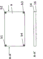
再次在另一实施例中,如图3C中所示的,应用均匀的导电触敏层16。图3C的上部示出了该实施例的前视图(图3C的上部)并且图3C的下部示出了沿A-A’的截面形式的该实施例。文中所示的触摸面板包括:(透明)基板14的每个角处的导电电极b1、b2、b3以及b4,该基板涂覆有层16中的透明导电结构,以形成等电位表面。电压通过导电电极b1、b2、b3以及b4施加至透明的导电结构16,以在其上形成等电位表面。当手指接触触摸面板时(即,14的最上层)时,其吸引小量电流至触点,产生电压降。从每个角流动的电流与至触点的距离成正比。触点的X/Y位置通过控制器来计算,并被传输至用户界面装置。In yet another embodiment, as shown in Figure 3C, a uniform conductive touch
当指向装置接近面板,而没有直接接触面板时,电容式触摸面板还能够检测电场的变化。以这种方式,在垂直于面板的方向上进行检测是可行的,从而允许另外的输入信息。Capacitive touch panels are also capable of detecting changes in the electric field when a pointing device approaches the panel without directly touching the panel. In this way, detection is possible in a direction perpendicular to the panel, allowing additional input information.
对于应用由层16中的一个或多个电导体形成的图案,可以有几种选择。For applying the pattern formed by one or more electrical conductors in
优选地,使用易溶于溶液的导电聚合物膜来形成具有导电结构的层16,这是因为在应用对例如氧化铟锡的传统溅射沉积中所需的高温或低压时,基板20会降级。可以通过众所周知的处理步骤将这种膜构造为制作电阻触摸面板部件所需的期望结构。例如,在使用光化学方法对高掺杂聚苯胺(PANI)层进行图案化的情况下,可以通过掩膜经由深度UV曝光进行图案化,产生导电区域(<1kΩ/)和非导电区域(>1010kΩ/),如在G.H.Gelinck等人的Appl.Phys.Lett.77,1487-1489(2000)中更详细地描述的,通过引证将其相关教导具体结合在此。如果需要,则可以在电泳薄片20和层16中的透明电结构之间设置附加层(未示出),例如,用作阻挡层或粘合层(参见图2B),或另一功能元件。代替聚苯胺,可以使用用于层16的其他透明导电层材料,例如聚噻吩、多吡咯或掺杂聚合物。除有机材料以外,还可以使用各种无机透明导电材料,如ITO(氧化铟锡)、IZO(氧化铟锌)、ATO(氧化锑锡)、或氧化锡。其他金属氧化物可以起作用,包括但不限于:氧化镍钨、铟掺杂氧化锌、氧化镁铟。此外,包含化合物的其他透明金属可认为是导电层。可以使用众所周知的溶液涂覆技术(如旋涂、喷涂、缝涂、或者印刷)来溅射、蒸发、电化学涂布、化学气相沉积或涂布无机材料作为纳米颗粒。优选地,这些纳米颗粒为纳米管的形式,这是因为其相对低的浓度已经导致良好的导电性。于是,层16中的颗粒对光的吸收相对较低。Preferably, a conductive polymer film that is readily soluble in solution is used to form the
优选地,以分离的过程将导电结构应用在层16中并且随后将层16应用至显示层。通常,对于像某些沉积步骤中所需的更低的压力、更高的温度或UV光的某些处理条件,膜14与显示结构相比更不敏感。Preferably, the conductive structure is applied in
优选地,使用粘合层13将诸如PET或PEN层的透明保护膜14或聚合物结构应用在触敏层16的顶部上。在优选的实施例中,粘合层为聚亚胺酯层。这种材料可以在相对低的温度下(小于70℃)固化。然而,也可以应用诸如UV固化粘合剂的其他粘合剂。透明保护膜14的厚度优选地为小于150μm,更优选地,25~50μm,最优选地,在12.5~25μm的范围内。可选地,顶部基板14可以设置有附加的具有光学功能的、机械保护或化学保护的涂层(15),如:防反射、防眩、硬化层、防污、UV保护、化学防护、防蒸气等。因而,这种层的应用是众所周知的。通常,附加层15的厚度基本小于膜14的厚度。Preferably, a transparent
在优选实施例中,如图2B中所示的,通过粘合层13将触敏结构22耦接至显示层20。与图2A中的那些相对应的部分具有相同的参考标号。In a preferred embodiment, touch
可以通过如印刷、光刻法、剥离、经由阴影掩膜的沉积等的各种传统方法来制造20和14上的导电母线和轨道。The conductive bus bars and tracks on 20 and 14 can be fabricated by various conventional methods such as printing, photolithography, lift-off, deposition through a shadow mask, and the like.
图4A和图4B示出了本发明的其他实施例。其中与图2A和图2B中的那些相对应的部分具有相同的参考标号。4A and 4B illustrate other embodiments of the present invention. Parts therein corresponding to those in FIGS. 2A and 2B have the same reference numerals.
在这些其他的实施例中,滤色片31应用在显示层20的顶部上。如果需要,可在进一步处理之前,将用于滤色片层的平面化层或保护层(如,负性抗蚀剂聚合物膜或者UV或热固化丙烯酸膜)32应用在滤色片31上。这种层防止具有多层的显示结构与触敏结构的化学相互作用。如图2A所示,可以通过相同的材料和相同的处理步骤来涂布触敏结构22的具有导电结构的层16。备选地,如图4B的实施例所示,可以交换粘合层13和层16的位置。在这种情况下,首先,平面化层32首先设置有具有导电结构的层16,并且最后,由经由粘合剂13的顶部基板14或具有附加涂层15的顶部基板14覆盖。In these other embodiments, a color filter 31 is applied on top of the
图4A和图4B的实施例具有附加的优点在于,与具有导电结构的层16配合执行触敏功能的前端基板14,还用作滤色片31的保护层。The embodiment of FIGS. 4A and 4B has the additional advantage that the
在US 6 850 355中同样更详细地描述了使用滤色片的电泳显示器。Electrophoretic displays using color filters are likewise described in more detail in US 6 850 355 .
图5A和图5B中示出了另外的实施例。图5A示意性地示出了面板的截面图,而图5B示意性地示出了面板的前视图。此处与图4A和图4B中的那些部分相对应的部分具有相同的参考标号。Additional embodiments are shown in Figures 5A and 5B. Fig. 5A schematically shows a cross-sectional view of the panel, while Fig. 5B schematically shows a front view of the panel. Parts here that correspond to those in FIGS. 4A and 4B have the same reference numerals.
在本文示出的实施例中,基板21具有在显示层20之外的至少一个方向上伸展的并且设置有导电元件24a、24b的伸展部21a,其中,上述两个导电元件将层16中的电导体16p的部分16x、16y耦接至伸展部21a的边缘21x处的各个触点25a、25b。为了清晰,将显示层20示为单层。然而,显示层可以由多重的子层组成,如参照图2A、2B以及4A、4B更详细地示出的。In the embodiment shown here, the
可以非常有效地制造根据本实施例的面板。优选地,图6中所示的这种方法包括以下步骤。Panels according to this embodiment can be manufactured very efficiently. Preferably, the method shown in Fig. 6 includes the following steps.
在步骤S1中,提供具有上述导电元件24a、24b的第一基板21。In step S1, the
在步骤S2中,将显示层20应用在所述第一基板21上。In step S2 , the
在步骤S3中,提供第二基板14。In step S3, a
在步骤S4中,将导电材料16p的图案应用在包括至少一个电导体的上述第二基板14上。In step S4, a pattern of electrically
在步骤S5中,通过面向导电材料16p的图案的显示层20将第一基板21粘附至第二基板14。优选地,至少部分电导体16p是免于粘合剂的,以得能够与基板21中的导电元件24a、24b抗性(resistive)接触。然而,可以设计成将电导体16p和导电元件24a、24b与作为电介质的非导电粘合剂进行电容连接。In step S5, the
在步骤S6中,基板24a(图5A和图5B)的伸展部设置有寻址显示层的地址解码元件28a、28b。地址解码元件包括:行解码器28a和列解码器28b。In step S6, the stretched portion of the
步骤S1~S6不需要必须以以上所提出的顺序来执行。备选地,可以在步骤S1和S2之前执行步骤S3和S4,或者可以与步骤S1和S2同时应用步骤S3、S4。Steps S1-S6 do not necessarily have to be performed in the order presented above. Alternatively, steps S3 and S4 may be performed before steps S1 and S2, or steps S3, S4 may be applied simultaneously with steps S1 and S2.
在图5A和图5B的实施例中,触敏结构具有第一层16,该第一层具有面向第一基板21的、蜿蜒的电导体形式(如图3B所示)的导电结构16p。将导电图案16p的第一部分16x和第二部分16y配置为相对并与第一基板21的伸展部21a的相应的导电元件24a、24b一部分电连接。其优点在于,可以很容易地制造具有触敏结构22的导电结构16p的层16至数据处理设备8的电连接。In the embodiment of FIGS. 5A and 5B , the touch-sensitive structure has a
通过导电粘合剂,导电图案16p的部分16x、16y与其相应的导电元件部分耦接。导电粘合剂是众所周知的,例如,压敏型粘合剂(PSA)。具体地,使用3M、类型9703的导电胶带用作压敏粘合剂。这是具有各向异性导电性的压敏粘合剂转印胶带。这是可以在室温与70℃之间的温度下应用的填充丙烯酸胶带。在24小时内建立粘性。可以使用的另一材料为Norland导电粘合剂NCA 130,其为可以通过UV光固化的并且包含用于固化没有被UV光曝光的区域的潜在的热催化剂的银填充(silver filled)各向同性导电粘合剂。可以选择各种备选的导电粘合剂。
图5A、5B中所示的电子装置的实施例中,基板24a的伸展部设置有用于寻址显示层的地址解码元件28a、28b。地址解码元件包括行解码器28a和列解码器28b。其优点在于,边缘21x处用于寻址显示层的触点25c、25d的数量是适度的。因此,这些触点可以相对较大,其能够简单并且快速地装配至其他组件。In the embodiment of the electronic device shown in Figures 5A, 5B, the extension of the
图5C示出了具有显示结构20的基板21的顶视图。图5D示出了具有包含导电结构的层16的触敏结构22的顶视图。图5E示出了集成在柔性显示面板3中的基板21、显示结构20以及触敏结构22。FIG. 5C shows a top view of the
如之前参照图3C所述的,图7A~图7C示出了怎样将另一触敏结构22(图7B)与基板21上的显示结构20(图7A)集成在显示面板3(图7C)中。在该实施例中,如图3C所示,触敏结构22具有包含触敏结构的层16。以在图5A~图5E中所示的类似的方式,将部分16q、16r、16s、16t电耦接至在基板21的伸展部中的电导体的相应部分24q、24r、24s、24t。As previously described with reference to FIG. 3C , FIGS. 7A to 7C show how to integrate another touch-sensitive structure 22 ( FIG. 7B ) with the display structure 20 ( FIG. 7A ) on the
在另一实施例中,通过分离的导线(例如,通过使用导线或使用分离的电线薄片(flex foil))来获得触敏结构的导电层16与装置的直接电接触,而不需要显示结构上的导电区域。In another embodiment, direct electrical contact between the
应注意,显示结构的固定电极20d还可以用作触敏结构的导电层16。在这种情况下,参照图2A,省略层20e并且用单个导电层18代替层16和20d。在这种情况下,电极18具有双重功能,在一侧上用作显示结构20中的用于显示效果的驱动电极,在另一侧上用作用于电容式触敏结构22的电极。电极18没有必要为均匀层。备选地,假设图案中的细节基本小于显示元件20a的尺寸或图案与该显示元件很好地排列,则可以以图案形式应用电极18,如图3A~图3C所示。It should be noted that the fixed
图8示意性地示出了耦接至共用电极18的电子电路的实施例。电子电路100包括由例如适当的应用软件控制的数据处理设备110。数据处理设备110控制用于驱动共用电极18的显示驱动器120。数据处理设备110进一步耦接至用于驱动共用电极18并从电极18读取输出信号的触敏驱动器130。开关元件140将显示驱动器120和触敏驱动器130交替地耦接至共用电极18。优选地,在1Hz~100Hz的频率范围内切换开关。在低于1Hz的频率处,不连续地更新显示信息,使其为用户可视。在高于100Hz的频率处,在触摸位置的处理期间可能出现干扰,这是因为切换开关元件140的频率太接近于触摸屏驱动器130驱动共用电极18的频率。当使用诸如电泳E Ink材料的多稳态显示效果时,关闭显示驱动系统将不会影响屏幕上的图像。因为多稳态性,所以图像得以保持。当在触敏模式下时,出现在共用电极上的信号也不会影响屏幕上的图像,这是因为电压可以相当小并且频率将超出电泳显示材料的响应带宽,通常至少高于因数10。FIG. 8 schematically shows an embodiment of an electronic circuit coupled to the
在另一实施例中,如图8A中所示,通过叠加元件145来代替开关元件140,该叠加元件将来自显示驱动器120和触摸屏驱动器130的驱动信号叠加为用于驱动共用电极18的叠加信号。In another embodiment, as shown in FIG. 8A , the switching
例如,显示驱动器120提供例如恒定电压,而触摸屏驱动器130提供高频信号。在连接至电极(如图7中所示的16q、16r、16s以及16t)的反馈线处测量输出信号,以指示在屏幕附近的指向目标的位置。假设高频信号的频率基本高于显示元件的响应频率或者在超过人类视觉系统的灵敏频率范围的范围内,则不会出现对显示图像上的触摸屏驱动信号的可视性的干扰。For example, the
图9示出了本发明的各种应用实施例。电子装置1A具有以含接合部9B的载体9A的形式存在的设备,接合部用于使显示器3绕电子装置的主壳体9缠绕。Fig. 9 shows various application embodiments of the present invention. The
电子装置1B具有:用于以卷的方式紧凑地存放显示面板3的第一壳体9D和用于包括数据处理设备的第二壳体9E。The
处于紧凑形状的显示器3仍具有可见部3A。可以添加机械保护单元9F来保护可见部3A。优选地,保护单元9F是透明的。The
同样地,电子装置1C具有:用于以卷的形式紧凑地存放显示面板3的第一壳体9D和包括数据处理设备的第二壳体9E。在该实施例中,通过第一壳体9D将显示面板完全地封装为其紧凑状态。Likewise, the
不需要触敏结构覆盖整个显示结构。例如,触敏结构可以用于仿真面板边缘处的选择按钮。在该实施例中,触敏结构仅需覆盖显示结构的小部分。面板可以设置有附加的支撑结构以支撑显示结构的上述小部分。There is no need for the touch-sensitive structure to cover the entire display structure. For example, touch-sensitive structures can be used to simulate selection buttons at the edge of a panel. In this embodiment, the touch sensitive structure need only cover a small portion of the display structure. The panel may be provided with additional support structures to support the aforementioned small parts of the display structure.
在权利要求中,单词“包括”不排除其他元件或者步骤,并且不定冠词“一(a)”或者“一(an)”不排除多个。单个组件或者其他单元可以实现权利要求中所列举的几项的功能。在相互不同的权利要求中列举的某些测量值的事实并不表示为了达到优点不可以使用这些测量的组合。权利要求中的任何参考标号不应解释为限制了范围。In the claims, the word "comprising" does not exclude other elements or steps and the indefinite article "a" or "an" does not exclude a plurality. A single component or other unit may fulfill the functions of several items recited in the claims. The mere fact that certain measures are recited in mutually different claims does not indicate that a combination of these measures cannot be used to advantage. Any reference signs in the claims should not be construed as limiting the scope.
Claims (22)
Applications Claiming Priority (3)
| Application Number | Priority Date | Filing Date | Title |
|---|---|---|---|
| US1359207P | 2007-12-13 | 2007-12-13 | |
| US61/013,592 | 2007-12-13 | ||
| PCT/NL2008/050797 WO2009075577A1 (en) | 2007-12-13 | 2008-12-12 | Electronic device with a flexible panel and method for manufacturing a flexible panel |
Publications (2)
| Publication Number | Publication Date |
|---|---|
| CN101946220A CN101946220A (en) | 2011-01-12 |
| CN101946220B true CN101946220B (en) | 2013-01-16 |
Family
ID=40527588
Family Applications (1)
| Application Number | Title | Priority Date | Filing Date |
|---|---|---|---|
| CN2008801266908A Active CN101946220B (en) | 2007-12-13 | 2008-12-12 | Electronic device with a flexible panel |
Country Status (4)
| Country | Link |
|---|---|
| US (2) | US9215301B2 (en) |
| CN (1) | CN101946220B (en) |
| TW (1) | TWI428869B (en) |
| WO (1) | WO2009075577A1 (en) |
Families Citing this family (76)
| Publication number | Priority date | Publication date | Assignee | Title |
|---|---|---|---|---|
| US20100156838A1 (en) * | 2008-12-18 | 2010-06-24 | Han Sang-Youl | Capacitive input display device |
| CN101924816B (en) * | 2009-06-12 | 2013-03-20 | 清华大学 | Flexible mobile phone |
| TWM368836U (en) * | 2009-07-01 | 2009-11-11 | Waltop Int Corp | Flexible tablet |
| US8576209B2 (en) | 2009-07-07 | 2013-11-05 | Semiconductor Energy Laboratory Co., Ltd. | Display device |
| TW201109769A (en) * | 2009-09-02 | 2011-03-16 | Ind Tech Res Inst | Multistable display system and method for writing image on multistable display |
| TWI396031B (en) * | 2009-10-02 | 2013-05-11 | Inventec Appliances Corp | Portable electronic device capable of containing electronic paper |
| GB2474689B (en) * | 2009-10-23 | 2015-08-26 | Plastic Logic Ltd | Electronic document reading devices |
| TWI410702B (en) * | 2010-02-10 | 2013-10-01 | Au Optronics Corp | Touch display panel |
| TWI410910B (en) * | 2010-08-02 | 2013-10-01 | Au Optronics Corp | Method of fabricating flexible display panel |
| US10831317B2 (en) * | 2010-08-20 | 2020-11-10 | Neodrón Limited | Electronic ink touch sensitive display |
| US20120062503A1 (en) * | 2010-09-14 | 2012-03-15 | Motorola-Mobility, Inc. | Device for integrating capactive touch with electrophoretic displays |
| US9213428B2 (en) | 2010-11-19 | 2015-12-15 | Blackberry Limited | Portable electronic device including flexible display |
| EP2456175B1 (en) * | 2010-11-19 | 2014-01-15 | BlackBerry Limited | Portable electronic device including flexible display |
| US8970512B2 (en) | 2010-12-22 | 2015-03-03 | Creator Technology B.V. | Touch screen display and method of driving the touch screen display with signal adjustment |
| TWI451181B (en) * | 2011-05-02 | 2014-09-01 | E Ink Holdings Inc | An electronic paper display apparatus with touch control function |
| US8953327B1 (en) * | 2011-05-26 | 2015-02-10 | iBlaidZ, Inc. | Self-winding membrane device |
| US9286812B2 (en) | 2011-06-07 | 2016-03-15 | Microsoft Technology Licensing, Llc | Flexible display extendable assembly |
| US20120313902A1 (en) * | 2011-06-10 | 2012-12-13 | Mao-Sung Wu | Capacitive touch structure |
| US20120313883A1 (en) * | 2011-06-10 | 2012-12-13 | Mao-Sung Wu | Capacitive touch device |
| EP2535791A3 (en) | 2011-06-17 | 2015-10-07 | Creator Technology B.V. | Electronic device with a touch sensitive panel, method for operating the electronic device, and display system |
| US8599158B2 (en) * | 2011-06-29 | 2013-12-03 | Nokia Corporation | Multi-surface touch sensitive apparatus and method |
| US10061356B2 (en) * | 2011-06-30 | 2018-08-28 | Samsung Display Co., Ltd. | Flexible display panel and display apparatus including the flexible display panel |
| KR101837714B1 (en) | 2011-08-10 | 2018-03-13 | 삼성디스플레이 주식회사 | Display device |
| US8711566B2 (en) | 2011-09-02 | 2014-04-29 | Microsoft Corporation | Expandable mobile device |
| US8665236B2 (en) | 2011-09-26 | 2014-03-04 | Apple Inc. | Electronic device with wrap around display |
| US10082826B1 (en) * | 2011-11-01 | 2018-09-25 | I-Blades, Inc. | Method and system for deploying a flexible device |
| KR20130056674A (en) * | 2011-11-22 | 2013-05-30 | 삼성전자주식회사 | Flexible display apparatus and method for providing user interface by using the same |
| TWI452553B (en) | 2011-12-30 | 2014-09-11 | Au Optronics Corp | Method of making a flexible display device |
| US9052414B2 (en) | 2012-02-07 | 2015-06-09 | Microsoft Technology Licensing, Llc | Virtual image device |
| US9354748B2 (en) | 2012-02-13 | 2016-05-31 | Microsoft Technology Licensing, Llc | Optical stylus interaction |
| US9158383B2 (en) | 2012-03-02 | 2015-10-13 | Microsoft Technology Licensing, Llc | Force concentrator |
| US9870066B2 (en) | 2012-03-02 | 2018-01-16 | Microsoft Technology Licensing, Llc | Method of manufacturing an input device |
| US8873227B2 (en) | 2012-03-02 | 2014-10-28 | Microsoft Corporation | Flexible hinge support layer |
| US9075566B2 (en) | 2012-03-02 | 2015-07-07 | Microsoft Technoogy Licensing, LLC | Flexible hinge spine |
| KR102014791B1 (en) * | 2012-03-27 | 2019-10-21 | 엘지전자 주식회사 | Optimization of application execution based on length of pulled out flexible display screen |
| US8724304B2 (en) * | 2012-04-20 | 2014-05-13 | Apple Inc. | Electronic devices with flexible displays having fastened bent edges |
| US20130300590A1 (en) | 2012-05-14 | 2013-11-14 | Paul Henry Dietz | Audio Feedback |
| US10031556B2 (en) | 2012-06-08 | 2018-07-24 | Microsoft Technology Licensing, Llc | User experience adaptation |
| US9019615B2 (en) | 2012-06-12 | 2015-04-28 | Microsoft Technology Licensing, Llc | Wide field-of-view virtual image projector |
| KR101383092B1 (en) * | 2012-06-27 | 2014-04-17 | 삼성디스플레이 주식회사 | Display device and driving method thereof |
| TWI461984B (en) * | 2012-07-12 | 2014-11-21 | Hannstouch Solution Inc | Flexible touch sensing display panel |
| US9355345B2 (en) | 2012-07-23 | 2016-05-31 | Microsoft Technology Licensing, Llc | Transparent tags with encoded data |
| US8952911B2 (en) * | 2012-08-08 | 2015-02-10 | Creator Technology B.V. | Electronic device with a touch sensitive panel, method for operating the electronic device, and display system |
| US8964379B2 (en) | 2012-08-20 | 2015-02-24 | Microsoft Corporation | Switchable magnetic lock |
| KR20150046325A (en) * | 2012-09-14 | 2015-04-29 | 유니-픽셀 디스플레이스, 인코포레이티드 | Foldable multi-touch surface |
| US9152173B2 (en) | 2012-10-09 | 2015-10-06 | Microsoft Technology Licensing, Llc | Transparent display device |
| TWI474246B (en) * | 2012-11-07 | 2015-02-21 | Henghao Technology Co Ltd | Touch device |
| KR102107134B1 (en) * | 2012-11-14 | 2020-05-06 | 삼성전자주식회사 | Method for arranging for list in flexable display an electronic device thereof |
| US9513748B2 (en) * | 2012-12-13 | 2016-12-06 | Microsoft Technology Licensing, Llc | Combined display panel circuit |
| US9261262B1 (en) | 2013-01-25 | 2016-02-16 | Steelcase Inc. | Emissive shapes and control systems |
| US9759420B1 (en) | 2013-01-25 | 2017-09-12 | Steelcase Inc. | Curved display and curved display support |
| US11327626B1 (en) | 2013-01-25 | 2022-05-10 | Steelcase Inc. | Emissive surfaces and workspaces method and apparatus |
| US9638835B2 (en) | 2013-03-05 | 2017-05-02 | Microsoft Technology Licensing, Llc | Asymmetric aberration correcting lens |
| US9904425B2 (en) | 2013-05-10 | 2018-02-27 | Nokia Technologies Oy | Meandering interconnect on a deformable substrate |
| CN105247597B (en) * | 2013-06-11 | 2018-04-10 | 英派尔科技开发有限公司 | Display devices and how to use them |
| TWI488087B (en) * | 2013-06-14 | 2015-06-11 | Au Optronics Corp | Input device |
| JP6121812B2 (en) * | 2013-06-25 | 2017-04-26 | 株式会社ジャパンディスプレイ | Liquid crystal display with touch panel |
| US9189028B2 (en) * | 2013-07-01 | 2015-11-17 | Serguei Nakhimov | Portable computer-communicator device with rollable display |
| KR101450638B1 (en) | 2013-10-31 | 2014-10-15 | 한밭대학교 산학협력단 | Pen-type mobile phone |
| US9337881B2 (en) * | 2013-11-22 | 2016-05-10 | Motorola Solutions, Inc. | Apparatus for providing information on a top section of a portable radio |
| US10120420B2 (en) | 2014-03-21 | 2018-11-06 | Microsoft Technology Licensing, Llc | Lockable display and techniques enabling use of lockable displays |
| GB2526298A (en) * | 2014-05-20 | 2015-11-25 | Nokia Technologies Oy | An apparatus and method wherein the apparatus comprises a flexible display and a flexible touch sensitive module |
| US10324733B2 (en) | 2014-07-30 | 2019-06-18 | Microsoft Technology Licensing, Llc | Shutdown notifications |
| US9684339B2 (en) | 2015-02-03 | 2017-06-20 | Microsoft Technology Licensing, Llc | Bendable display assembly |
| KR102304310B1 (en) * | 2015-02-13 | 2021-09-23 | 삼성디스플레이 주식회사 | Rollable display device |
| US10082913B2 (en) * | 2015-05-10 | 2018-09-25 | Microsoft Technology Licensing, Llc | Embroidered sensor assembly |
| WO2017006994A1 (en) * | 2015-07-09 | 2017-01-12 | シャープ株式会社 | Active matrix substrate, display device and production method |
| TWI634702B (en) | 2016-05-11 | 2018-09-01 | 財團法人工業技術研究院 | Structure constructed by sheet |
| CN106098735B (en) * | 2016-06-20 | 2020-10-09 | 武汉华星光电技术有限公司 | OLED display screen |
| TWI651021B (en) | 2016-11-28 | 2019-02-11 | 財團法人工業技術研究院 | Flexible electronic device |
| US10264213B1 (en) | 2016-12-15 | 2019-04-16 | Steelcase Inc. | Content amplification system and method |
| US10444912B2 (en) | 2016-12-30 | 2019-10-15 | Industrial Technology Research Institute | Sensing method of sensing device and stretchable sensor device |
| KR102504138B1 (en) * | 2018-01-04 | 2023-03-02 | 삼성디스플레이 주식회사 | Rollable display device |
| KR102518748B1 (en) * | 2018-01-05 | 2023-04-07 | 삼성디스플레이 주식회사 | Rollable display device |
| CN108111652B (en) * | 2018-02-09 | 2019-09-20 | 浙江工贸职业技术学院 | A kind of mobile phone that can adjust screen size |
| CN113301196B (en) * | 2021-05-24 | 2024-03-08 | 维沃移动通信有限公司 | Electronic equipment |
Citations (3)
| Publication number | Priority date | Publication date | Assignee | Title |
|---|---|---|---|---|
| WO2002047363A2 (en) * | 2000-12-05 | 2002-06-13 | E Ink Corporation | Portable eclectronic apparatus with additional electro-optical display |
| CN1672119A (en) * | 2002-07-23 | 2005-09-21 | 3M创新有限公司 | Thin face capacitive touch screen |
| CN1826576A (en) * | 2003-07-21 | 2006-08-30 | 皇家飞利浦电子股份有限公司 | Touch sensitive display for a portable device |
Family Cites Families (14)
| Publication number | Priority date | Publication date | Assignee | Title |
|---|---|---|---|---|
| US5528267A (en) * | 1988-12-19 | 1996-06-18 | Sharp Kabushiki Kaisha | Tablet integrated with display |
| JP2004519008A (en) * | 2001-02-08 | 2004-06-24 | コーニンクレッカ フィリップス エレクトロニクス エヌ ヴィ | Display cell manufacturing method |
| KR100642183B1 (en) | 2001-08-22 | 2006-11-06 | 샤프 가부시키가이샤 | Touch sensor, display device with touch sensor, and location data generation method |
| US7050835B2 (en) * | 2001-12-12 | 2006-05-23 | Universal Display Corporation | Intelligent multi-media display communication system |
| AU2003302796A1 (en) * | 2002-12-10 | 2004-06-30 | Koninklijke Philips Electronics N.V. | Display device and electronic appliance for use in combination therewith |
| US8068186B2 (en) * | 2003-10-15 | 2011-11-29 | 3M Innovative Properties Company | Patterned conductor touch screen having improved optics |
| US7208691B2 (en) * | 2004-11-12 | 2007-04-24 | Eastman Kodak Company | Touch screen having undercut spacer dots |
| US20070085837A1 (en) * | 2005-10-17 | 2007-04-19 | Eastman Kodak Company | Touch input device with display front |
| KR20070063314A (en) * | 2005-12-14 | 2007-06-19 | 삼성전자주식회사 | Display device and manufacturing method |
| US8477250B2 (en) * | 2005-12-16 | 2013-07-02 | Creator Technology B.V. | Circular displays |
| US7639237B2 (en) * | 2006-03-03 | 2009-12-29 | Perkins Michael T | Roll-out touch screen support system (ROTS3) |
| US8373664B2 (en) * | 2006-12-18 | 2013-02-12 | Cypress Semiconductor Corporation | Two circuit board touch-sensor device |
| EP2026178A1 (en) * | 2007-08-10 | 2009-02-18 | IEE INTERNATIONAL ELECTRONICS & ENGINEERING S.A. | Touchpad with strip-shaped input |
| KR101002308B1 (en) * | 2008-09-12 | 2010-12-17 | 엘지디스플레이 주식회사 | Liquid crystal display |
-
2008
- 2008-12-12 CN CN2008801266908A patent/CN101946220B/en active Active
- 2008-12-12 WO PCT/NL2008/050797 patent/WO2009075577A1/en not_active Ceased
- 2008-12-12 US US12/747,854 patent/US9215301B2/en active Active
- 2008-12-15 TW TW097148873A patent/TWI428869B/en not_active IP Right Cessation
-
2015
- 2015-11-16 US US14/942,821 patent/US10572074B2/en active Active
Patent Citations (3)
| Publication number | Priority date | Publication date | Assignee | Title |
|---|---|---|---|---|
| WO2002047363A2 (en) * | 2000-12-05 | 2002-06-13 | E Ink Corporation | Portable eclectronic apparatus with additional electro-optical display |
| CN1672119A (en) * | 2002-07-23 | 2005-09-21 | 3M创新有限公司 | Thin face capacitive touch screen |
| CN1826576A (en) * | 2003-07-21 | 2006-08-30 | 皇家飞利浦电子股份有限公司 | Touch sensitive display for a portable device |
Also Published As
| Publication number | Publication date |
|---|---|
| US20110043479A1 (en) | 2011-02-24 |
| US10572074B2 (en) | 2020-02-25 |
| TWI428869B (en) | 2014-03-01 |
| US9215301B2 (en) | 2015-12-15 |
| WO2009075577A1 (en) | 2009-06-18 |
| TW200933558A (en) | 2009-08-01 |
| CN101946220A (en) | 2011-01-12 |
| US20160077633A1 (en) | 2016-03-17 |
Similar Documents
| Publication | Publication Date | Title |
|---|---|---|
| CN101946220B (en) | Electronic device with a flexible panel | |
| CN103576983B (en) | Electronic display unit and image display system | |
| EP2843519B1 (en) | Touch window and touch device including the same | |
| KR102456154B1 (en) | Sensor, touch sensor and display device | |
| CN102707831B (en) | Touch pad and the touch-screen with this touch pad | |
| CN102681723B (en) | Touch screen | |
| EP2473902B1 (en) | Touch screen and method for manufacturing a touch screen | |
| JPWO2016151426A1 (en) | Display device, electronic device, and system | |
| KR20120076365A (en) | Electro-optic displays with touch sensors | |
| CN103415830A (en) | Touch panel, method for manufacturing the same, and liquid crystal display device including the touch panel | |
| GB2559575A (en) | Touch sensor | |
| WO2013084087A1 (en) | System and method for identifying the shape of a display device | |
| JP2015118682A (en) | Touch panel | |
| CN103941896B (en) | Touch panel and touch display device | |
| CN107621902A (en) | Pressure sensor and display device including same | |
| CN111124171B (en) | Pressure sensor and display device having the same |
Legal Events
| Date | Code | Title | Description |
|---|---|---|---|
| C06 | Publication | ||
| PB01 | Publication | ||
| C10 | Entry into substantive examination | ||
| SE01 | Entry into force of request for substantive examination | ||
| ASS | Succession or assignment of patent right |
Owner name: CREATOR TECHNOLOGY CO., LTD. Free format text: FORMER OWNER: KONINKL PHILIPS ELECTRONICS NV Effective date: 20110720 |
|
| C41 | Transfer of patent application or patent right or utility model | ||
| COR | Change of bibliographic data |
Free format text: CORRECT: ADDRESS; FROM: EINDHOVEN, NETHERLANDS TO: BREDA, NETHERLANDS |
|
| TA01 | Transfer of patent application right |
Effective date of registration: 20110720 Address after: Holland buleda Applicant after: Creator Technology B. V. Address before: Holland Ian Deho Finn Applicant before: Koninkl Philips Electronics NV |
|
| C14 | Grant of patent or utility model | ||
| GR01 | Patent grant | ||
| C41 | Transfer of patent application or patent right or utility model | ||
| TR01 | Transfer of patent right |
Effective date of registration: 20160414 Address after: Gyeonggi Do, South Korea Patentee after: Samsung Electronics Co., Ltd. Address before: Holland buleda Patentee before: Creator Technology B. V. |