CN101888554B - VLSI (Very Large Scale Integration) structure design method for parallel flowing motion compensating filter - Google Patents
VLSI (Very Large Scale Integration) structure design method for parallel flowing motion compensating filter Download PDFInfo
- Publication number
- CN101888554B CN101888554B CN 201010222854 CN201010222854A CN101888554B CN 101888554 B CN101888554 B CN 101888554B CN 201010222854 CN201010222854 CN 201010222854 CN 201010222854 A CN201010222854 A CN 201010222854A CN 101888554 B CN101888554 B CN 101888554B
- Authority
- CN
- China
- Prior art keywords
- reference pixel
- pixel data
- data
- memory
- block
- Prior art date
- Legal status (The legal status is an assumption and is not a legal conclusion. Google has not performed a legal analysis and makes no representation as to the accuracy of the status listed.)
- Expired - Fee Related
Links
Images


Landscapes
- Compression Or Coding Systems Of Tv Signals (AREA)
Abstract
本发明公开了一种并行流水运动补偿滤波器VLSI结构设计方法。采用运动补偿模块亮度像素点与色度像素点并行计算的方式,采用自适应块内在流水线处理方式,减少整个解码的处理时间,提高了系统吞吐量。采用对片上存储器分层构架设计,对访问方式做了进一步优化,减少对片外存储器的访问。采用参考像素的数据复用技术,采用更新子宏块处理技术,显著节约了读取数据所用时间,减少了数据读取带宽,从而提高解码器的解码效率,提高解码性能。
The invention discloses a VLSI structure design method of a parallel pipeline motion compensation filter. The method of parallel calculation of luma pixel and chroma pixel of the motion compensation module is adopted, and the internal pipeline processing method of adaptive block is adopted, which reduces the processing time of the whole decoding and improves the system throughput. The layered architecture design of the on-chip memory is adopted, and the access method is further optimized to reduce the access to the off-chip memory. Using the data multiplexing technology of reference pixels and the update sub-macroblock processing technology can significantly save the time for reading data and reduce the bandwidth of data reading, thereby improving the decoding efficiency of the decoder and improving the decoding performance.
Description
技术领域 technical field
本发明属于视频解码领域,特别涉及一种并行流水运动补偿滤波器VLSI结构设计方法。The invention belongs to the field of video decoding, in particular to a VLSI structure design method of a parallel pipeline motion compensation filter.
背景技术 Background technique
H.264视频编解码标准是当前国际上主流的编解码标准。作为新一代视频编码标准,H.264视频编码标准与过去的视频编码标准相比,编码构架基本相同,但是编码效率有了大幅度的提高。其代价是运算的过程更加复杂,计算量更大,这些都增大了视频解码器硬件实现的难度。所以,在设计视频解码芯片时,应当致力于提高解码效率,减少面积和功耗。但是,在视频解码领域中,设备的功耗与片上面积总是受到各种限制。既需要实现更复杂的解码算法,提高效率,又要减少面积、降低功耗,所以仍然存在许多挑战。运动补偿是利用参考图像恢复当前图像的一种技术,用来重构时间冗余信息,进而恢复出整个视频序列。在H.264的整个解码过程中,运动补偿占用的时间很高,该模块的特点是数据读取耗时,且计算量很大。H.264解码运动补偿运算所消耗的时间最多。特别是针对高清和超高清视频解码应用,设计高效实时的运动补偿滤波器成为研究热点。The H.264 video codec standard is currently the mainstream codec standard in the world. As a new generation of video coding standard, H.264 video coding standard has basically the same coding framework as previous video coding standards, but the coding efficiency has been greatly improved. The price is that the calculation process is more complicated and the calculation amount is larger, which increases the difficulty of hardware implementation of the video decoder. Therefore, when designing a video decoding chip, efforts should be made to improve decoding efficiency and reduce area and power consumption. However, in the field of video decoding, the power consumption and on-chip area of the device are always subject to various constraints. It is necessary to implement more complex decoding algorithms to improve efficiency, but also to reduce area and power consumption, so there are still many challenges. Motion compensation is a technology that uses reference images to restore the current image, which is used to reconstruct temporal redundant information, and then restore the entire video sequence. During the entire decoding process of H.264, motion compensation takes a lot of time. The characteristic of this module is that data reading is time-consuming and the amount of calculation is large. H.264 decoding motion compensation operation consumes the most time. Especially for high-definition and ultra-high-definition video decoding applications, designing efficient and real-time motion compensation filters has become a research hotspot.
发明内容 Contents of the invention
针对上述现有技术不足,本发明目的在于提供一种并行流水运动补偿滤波器VLSI结构设计方法。利用并行处理和数据复用的计算方式进行解码运动补偿,减少整个解码的处理时间,从而提高解码器的解码效率,提高解码性能。In view of the above-mentioned deficiencies in the prior art, the purpose of the present invention is to provide a VLSI structure design method of a parallel pipeline motion compensation filter. Using parallel processing and data multiplexing calculation methods to perform decoding motion compensation, reduce the processing time of the entire decoding, thereby improving the decoding efficiency of the decoder and improving the decoding performance.
为了实现上述任务,本发明采用的技术解决方案是:In order to realize above-mentioned task, the technical solution that the present invention adopts is:
从片外存储器的读取已解码出来的一个宏块的运动矢量与块划分类型控制流信息,存放到片上存储器上;Read the decoded motion vector and block division type control flow information of a macroblock from the off-chip memory, and store it in the on-chip memory;
根据已存放到片上存储器的这些控制流信息,从片外存储器读取需要运动补偿所对应子块的参考像素数据,并存放在分层片上存储器的参考像素数据存储器层,进行运动补偿,运动补偿分为亮度分量和色度分量两大模块,色度分量包括U分量和V分量,亮度分量采用六抽头滤波运算,色度分量采用双线性插值滤波运算,整个处理过程是将亮度和色度分量进行并行流水处理,亮度分量参考像素数据从片外存储器读取完毕之后,直接进入色度的U分量参考像素数据的读取阶段,亮度分量的运算和色度的U分量参考像素数据读取在同一时刻开始进行,色度的U分量运算完毕后,紧接着进行色度的V分量参考像素读取和运算,当完成色度的两个分量的运算之后,再次进行亮度分量参考像素数据的读取,一个宏块运动补偿完毕,再次从片外存储器读取下一个宏块的控制流信息,用于该宏块运动补偿。According to the control flow information that has been stored in the on-chip memory, read the reference pixel data of the corresponding sub-block that needs motion compensation from the off-chip memory, and store it in the reference pixel data memory layer of the layered on-chip memory for motion compensation and motion compensation It is divided into two modules: luminance component and chroma component. The chroma component includes U component and V component. The luminance component adopts six-tap filter operation, and the chroma component adopts bilinear interpolation filter operation. The components are processed in parallel pipeline. After the brightness component reference pixel data is read from the off-chip memory, it directly enters the reading stage of the U component reference pixel data of the chroma, and the operation of the brightness component and the U component reference pixel data of the chroma are read. Start at the same time. After the U component of the chroma is calculated, the reference pixel of the V component of the chroma is read and calculated. After the calculation of the two components of the chroma is completed, the reference pixel data of the luminance component is read again. Read, after the motion compensation of a macro block is completed, the control flow information of the next macro block is read from the off-chip memory again for the motion compensation of the macro block.
所述运动矢量描述了当前块运动估计运算的结果,运动越剧烈,运动矢量数值越大,块划分类型代表当前块的长和宽。The motion vector describes the result of the motion estimation operation of the current block. The more severe the motion, the larger the value of the motion vector, and the block division type represents the length and width of the current block.
所述的分层片上存储器分为三层,包括参考像素数据存储器层、中间结果存储器层及数据复用存储器层,参考像素数据存储器层分为亮度和色度存储片,存放从片外存储器读取的亮度和色度参考像素数据,亮度运算过程中经常碰到需要保存中间结果的情况,需要将这些数据存放于中间结果存储器层上,作为下一次滤波运算的输入量,子宏块亮度和色度分量运算完毕,再次进行亮度分量参考像素数据的读取,子宏块的亮度参考像素数据从片外存储器的读取与更新十分耗时,而相邻的子宏块的参考像素有着很大程度的交叠,在更新参考帧数据时应该合理的安排更新顺序,复用片上存储器中已有的上一个子宏块的参考像素数据,存放到分层片上存储器的数据复用存储器层上,在当前子宏块运动补偿运算完毕,下一子宏块运动补偿运算开始时,先进行判断,如果可以实现数据复用,则先将数据复用存储器的数据写入参考像素数据存储器中,再从片外存储器读取其余参考像素。The layered on-chip memory is divided into three layers, including a reference pixel data memory layer, an intermediate result memory layer, and a data multiplexing memory layer. The fetched luminance and chrominance refer to pixel data. In the process of luminance calculation, intermediate results are often needed to be saved. These data need to be stored on the intermediate result memory layer as the input of the next filtering operation. The sub-macroblock luminance and After the calculation of the chrominance component is completed, read the reference pixel data of the luma component again. It is very time-consuming to read and update the luma reference pixel data of the sub-macroblock from the off-chip memory, and the reference pixels of the adjacent sub-macroblocks have a large For a large degree of overlap, the update order should be arranged reasonably when updating the reference frame data, and the reference pixel data of the previous sub-macroblock existing in the on-chip memory is multiplexed and stored in the data multiplexing memory layer of the layered on-chip memory , when the motion compensation calculation of the current sub-macroblock is completed and the motion compensation calculation of the next sub-macroblock starts, a judgment is made first, and if data multiplexing can be realized, the data in the data multiplexing memory is first written into the reference pixel data memory, The remaining reference pixels are then read from off-chip memory.
本发明实现色度和亮度的并行解码,提高并行解码的效率和速度,减少对片外存储器的访问,节约了读取数据所用时间,减少了数据带宽,以实现实时高清视频解码,适应高清视频应用的发展。The invention realizes parallel decoding of chroma and brightness, improves the efficiency and speed of parallel decoding, reduces access to off-chip memory, saves the time used for reading data, and reduces data bandwidth, so as to realize real-time high-definition video decoding and adapt to high-definition video application development.
附图说明 Description of drawings
图1是运动补偿模块的体系架构示意图。FIG. 1 is a schematic diagram of the architecture of the motion compensation module.
图2是运动补偿内在流水线计算处理示意图。Fig. 2 is a schematic diagram of motion compensation internal pipeline calculation processing.
图3是亮度分量的三层存储器结构示意图。FIG. 3 is a schematic diagram of a three-layer memory structure of a luminance component.
图4是更新处理顺序数据复用示意图。Fig. 4 is a schematic diagram of sequential data multiplexing in update processing.
图4(a)表示第1个8x8块参考像素。Figure 4(a) shows the first 8x8 block reference pixels.
图4(b)表示第2个8x8块参考像素。Figure 4(b) shows the second 8x8 block reference pixels.
图4(c)表示第1个8x8块和第2个8x8块的公共参考像素。Figure 4(c) shows the common reference pixels of the first 8x8 block and the second 8x8 block.
图4(d)表示第2个8x8块参考像素。Figure 4(d) shows the second 8x8 block reference pixels.
图4(e)表示第4个8x8块参考像素。Figure 4(e) shows the 4th 8x8 block reference pixels.
图4(f)表示第2个8x8块和第4个8x8块公共参考像素。Figure 4(f) shows the common reference pixels of the 2nd 8x8 block and the 4th 8x8 block.
具体实施方式Detailed ways
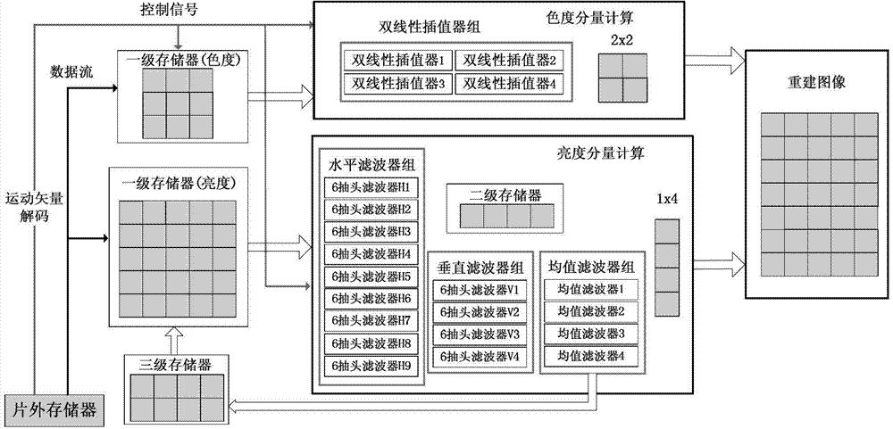
图1所示是运动补偿模块的整体架构设计图。在图中可以看到,本模块可大致分为三个部分。下面分别做以介绍。Figure 1 shows the overall architecture design of the motion compensation module. As can be seen in the figure, this module can be roughly divided into three parts. The following are introduced separately.
第一部分是模块输入输出接口。其中,输入接口是片外存储器,从中读取参考帧像素数据、运动矢量与块划分类型等信息。输出接口是向外存中写入重构好的当前帧数据,其中包含亮度与色度两个分量的数值。The first part is the module input and output interface. Among them, the input interface is an off-chip memory, from which information such as reference frame pixel data, motion vector and block division type is read. The output interface is to write the reconstructed current frame data into the external memory, which contains the values of two components of brightness and chrominance.
第二部分是分层的片上存储器,用来存放从外存读取的所需数据。为了减少读取带宽、提高数据复用率,同时,为了实现自适应的大小可变块处理,本文采用了三层片上缓存器结构,包括参考像素数据存储器层、中间结果存储器层及数据复用存储器层。第一层片上存储器作为参考像素数据存储器层,存放读入的参考帧数据,第二层片上存储器作为中间结果存储器层,存放滤波器运算的中间结果,第三层片上存储器作为数据复用存储器层,存放部分参考像素,以便重写到第一层片上存储器中参与下次运算。The second part is the hierarchical on-chip memory, which is used to store the required data read from the external memory. In order to reduce the read bandwidth and improve the data multiplexing rate, at the same time, in order to realize the self-adaptive variable size block processing, this paper adopts a three-layer on-chip buffer structure, including the reference pixel data memory layer, the intermediate result memory layer and data multiplexing storage layer. The first layer of on-chip memory is used as a reference pixel data memory layer to store the read-in reference frame data, the second layer of on-chip memory is used as an intermediate result memory layer to store intermediate results of filter operations, and the third layer of on-chip memory is used as a data multiplexing memory layer , storing part of the reference pixels so as to be rewritten into the first layer of on-chip memory to participate in the next operation.
第三部分是插值滤波器组,具体分为亮度运算和色度运算两大子模块。其中亮度部分的插值运算采用6抽头滤波器实现,多个6抽头滤波器构成了滤波器组,并且由水平滤波器组与垂直滤波器组进一步组成双滤波器组实现并行运算。这一设计结构能够在子宏块级别实现流水线处理,减少了整个宏块的插值计算时间。而色度部分的插值运算由双线性插值器实现,也采用了多个滤波器构成的滤波器组的设计结构。在整个运算的过程中,亮度与色度实现了并行化处理,从而减少整个解码时间,提高了运算效率。在处理过程中,无论亮度还是色度,都采用自适应可变块大小流水线方式进行处理。The third part is the interpolation filter bank, which is specifically divided into two sub-modules of luma operation and chroma operation. Among them, the interpolation operation of the luminance part is realized by a 6-tap filter, and a plurality of 6-tap filters constitute a filter bank, and a double filter bank is further composed of a horizontal filter bank and a vertical filter bank to realize parallel operation. This design structure can implement pipeline processing at the sub-macroblock level, reducing the interpolation calculation time of the entire macroblock. The interpolation operation of the chroma part is realized by a bilinear interpolator, and a design structure of a filter bank composed of multiple filters is also adopted. During the entire operation process, the brightness and chrominance are processed in parallel, thereby reducing the entire decoding time and improving the operation efficiency. In the process of processing, regardless of brightness or chrominance, the adaptive variable block size pipeline is used for processing.
图2所示是运动补偿流水计算处理示意图。FIG. 2 is a schematic diagram of motion compensation flow calculation processing.
视频处理分为YUV三个分量。按照H.264中的规定,Y分量采用六抽头滤波器进行计算,UV分量采用双线性插值进行计算。从图中可以看到,在Y分量进行运算的同时,U分量就已经开始读取参考数据了。这一结构可以节约计算时间。在以前的串行运算结构中,都是在亮度分量运算完毕后,才读取色度分量的数据进行运算的。Video processing is divided into three components of YUV. According to the regulations in H.264, the Y component is calculated using a six-tap filter, and the UV component is calculated using bilinear interpolation. It can be seen from the figure that while the Y component is operating, the U component has already started to read the reference data. This structure saves computation time. In the previous serial operation structure, the data of the chrominance component is read for operation after the operation of the luminance component is completed.
图3所示是亮度分量的三层存储器结构示意图。FIG. 3 is a schematic diagram of the three-layer memory structure of the brightness component.
从图中可以看到,整个处理过程包含三层存储器。每一层都担负着各自不同的功能。As can be seen from the figure, the entire processing process includes three layers of memory. Each layer is responsible for its own different functions.
首先,从片外存储器读取当前宏块解码所需要的数据,存放在第一层参考像素数据存储器层中,分为亮度存储片与色度存储片两个部分,具体包括参考帧像素数据、块类型划分、子宏块运动矢量等等。接下来,参考数据存储器中的数据作为输入,在滤波器组中进行运算。计算过程中经常碰到需要保存中间结果的情况,需要将这些数据存放于中间结果存储器层上,作为下一次滤波运算的输入量。在运算完毕后,重建好的像素点作为最终结果写到外部存储器上。为了实现数据的复用,加入了第三层片上存储器-数据复用存储器层,用来存储部分参考帧数据。这些数据可能用于下一个子宏块的运算。在当前子宏块运算完毕,下一子宏块运算开始时,先进行判断,如果可以实现数据复用,则先将第三层存储器的数据写入第一层存储器中,从而减少从外存读取数据的时间。不同层级的存储器之间协调工作,优化了整个模块的性能。First, read the data required for decoding the current macroblock from the off-chip memory, and store it in the first layer of reference pixel data memory layer, which is divided into two parts: luminance storage slice and chrominance storage slice, specifically including reference frame pixel data, Block type division, sub-macroblock motion vectors, etc. Next, refer to the data in the data memory as input, and perform operations in the filter bank. In the calculation process, it is often encountered that intermediate results need to be saved, and these data need to be stored on the intermediate result storage layer as the input of the next filtering operation. After the operation is completed, the reconstructed pixels are written to the external memory as the final result. In order to achieve data multiplexing, a third layer of on-chip memory-data multiplexing memory layer is added to store part of the reference frame data. These data may be used for the operation of the next sub-macroblock. When the operation of the current sub-macroblock is completed and the operation of the next sub-macroblock starts, a judgment is made first. If data multiplexing can be realized, the data of the third-level memory is first written into the first-level memory, thereby reducing the number of external storage operations. The time to read the data. The coordination between different levels of memory optimizes the performance of the entire module.
图4所示是更新处理顺序数据复用示意图。FIG. 4 is a schematic diagram of sequential data multiplexing in update processing.
运动补偿读取与更新数据十分耗时。但经过分析,发现这些子宏块的参考像素有着很大程度的交叠。因此,在更新参考帧数据时应该合理的安排更新顺序,尽量复用片上存储器中已有的数据,从而减少数据读取的时间。Reading and updating data for motion compensation is time consuming. However, after analysis, it is found that the reference pixels of these sub-macroblocks overlap to a large extent. Therefore, when updating the reference frame data, the update sequence should be arranged reasonably, and the existing data in the on-chip memory should be reused as much as possible, thereby reducing the time for data reading.
图4(a)、图4(b)、图4(c)中展示了处理前两个8x8子宏块时所需要的参考像素块,以及二者之间共有的参考数据区域。在第2个子宏块进行运动补偿时,不必读入所有参考帧数据,而是保存第1个子宏块参考数据中可以被复用部分(5x13像素块),仅更新右侧8x13块的数据。这样一来,更新数据的数量从13x13字节下降到8x13字节,降低了近40%,读取数据所需时间显著缩短。因此,在第一个8x8子块处理完毕时,右侧5x13的像素块数据将被保存在第3层片上存储器中,供处理下一个子块更新参考数据时取用。Fig. 4(a), Fig. 4(b) and Fig. 4(c) show the reference pixel blocks required for processing the first two 8x8 sub-macroblocks, and the shared reference data area between them. When performing motion compensation on the second sub-macroblock, it is not necessary to read all the reference frame data, but save the multiplexed part (5x13 pixel block) of the reference data of the first sub-macroblock, and only update the data of the 8x13 block on the right . In this way, the amount of update data is reduced from 13x13 bytes to 8x13 bytes, which is reduced by nearly 40%, and the time required to read data is significantly shortened. Therefore, when the first 8x8 sub-block is processed, the data of the 5x13 pixel block on the right side will be stored in the on-chip memory of the third layer, which can be accessed when processing the next sub-block to update the reference data.
为了进一步提高数据复用率,可以改变子宏块的处理顺序,在处理完第2个子宏块之后,先行处理第4个子宏块。图4(d)、图4(e)、图4(f)展示了这两个子宏块时所需要的参考像素块,以及二者之间共有的参考数据区域。由于第2个子宏块和第4个子宏块在空间上是相邻的,所以共用的像素点数多,大小仍为5x13的块。这样一来,处理完第4个子宏块后,再去处理第3个子宏块,此时复用的参考像素是第4个子宏块左侧5x13像素块。由于调整了子宏块的处理顺序,不仅是参考像素的读入顺序需要做改变,相应的当前子块运动矢量等等都需要做调整。In order to further improve the data multiplexing rate, the processing order of the sub-macroblocks can be changed, and after the second sub-macroblock is processed, the fourth sub-macroblock is processed first. FIG. 4(d), FIG. 4(e), and FIG. 4(f) show the reference pixel blocks required by these two sub-macroblocks, and the reference data area shared between them. Since the second sub-macroblock and the fourth sub-macroblock are spatially adjacent, the number of shared pixels is large, and the size is still a 5x13 block. In this way, after the fourth sub-macroblock is processed, the third sub-macroblock is processed. At this time, the reference pixel for multiplexing is the 5×13 pixel block on the left side of the fourth sub-macroblock. Due to the adjustment of the processing order of the sub-macroblocks, not only the reading order of the reference pixels needs to be changed, but also the corresponding current sub-block motion vector and the like need to be adjusted.
本发明提供了一种并行流水运动补偿滤波器VLSI结构设计方法,可以实现运动补偿模块亮度像素点与色度像素点并行流水计算,节约了总体的计算时间。另外,提出分层存储器构架设计,对访问方式做了进一步优化,提高了片上数据的复用率,从而显著节约了读取数据所用时间,同时减少了数据带宽。The invention provides a VLSI structural design method of a parallel pipeline motion compensation filter, which can realize the parallel pipeline calculation of brightness pixels and chrominance pixels of a motion compensation module, and save overall calculation time. In addition, a hierarchical memory architecture design is proposed, the access method is further optimized, and the data reuse rate on the chip is improved, thereby significantly saving the time for reading data and reducing the data bandwidth.
为了实现上述任务,本发明采用的技术解决方案是:In order to realize above-mentioned task, the technical solution that the present invention adopts is:
1)通过“并行技术”,实现亮度分量与色度分量的并行运动补偿解码,提高解码速度和效率;1) Through "parallel technology", realize parallel motion compensation decoding of luma component and chrominance component, improve decoding speed and efficiency;
2)通过“内在流水线技术”,提高系统吞吐量,不增加数据带宽。2) Through the "intrinsic pipeline technology", the system throughput is improved without increasing the data bandwidth.
3)通过“分层片上存储技术”,减少对片外存储的访问,实现三层片上存储器结构对数据进行复用。3) Through the "layered on-chip storage technology", the access to off-chip storage is reduced, and the three-layer on-chip memory structure is used to multiplex data.
4)通过“数据复用技术”,减少模块读取参考像素的时间。4) Through "data multiplexing technology", reduce the time for the module to read reference pixels.
5)通过“更新处理子宏块顺序技术”,实现了最大化的复用参考像素数据。5) Through the "updating and processing sub-macroblock sequence technology", the maximum multiplexing of reference pixel data is realized.
所述的“并行技术”是对亮度和色度运动补偿运算时间并行处理。由于亮度分量的处理与色度分量的处理二者之前没有数据依赖关系,所以可以将亮度和色度进行并行处理。在不增加数据读取带宽的条件下,可以在亮度分量数据准备完毕之后,直接进入色度分量数据的准备和运算阶段。通过亮度和色度同时运算,进一步缩短整个宏块的计算时间。The "parallel technique" mentioned is the time-parallel processing of luma and chrominance motion compensation calculations. Since there is no data dependency between the processing of the luma component and the processing of the chrominance component, the luma and chrominance can be processed in parallel. Under the condition of not increasing the data reading bandwidth, the preparation and calculation phase of the chrominance component data can be directly entered after the preparation of the luminance component data is completed. The calculation time of the whole macroblock is further shortened by simultaneous operation of luma and chrominance.
所述“内在流水线技术”是指系统采用自适应块的运算处理的流水线技术,分别对亮度和色度的读取数据进行的流水操作,提高了系统的吞吐量,减少了运算解码时间,提高了许多功能块的复用率。处理每一个子块的过程是分为两个部分:数据读取和数据运算,运算采用并行处理,而读取则是采用流水线处理。对亮度和色度分量的分别流水读取参考像素,在亮度分量数据准备完毕,并开始运动补偿运算时对色度的参考像素读取,实现流水,并且不增加数据带宽。对于亮度分量,当目前像素块大于或等于8x8大小时,按照8x8大小块进行处理,运算需要迭代4次;当小于8x8时,按照4x4块进行处理,运算需要迭代16次。对于色度分量,当目前像素块大小在4x4以上时,按照4x4块进行处理,迭代4次完成;当块大小在4x4以下是按照2x2块进行处理,迭代16次完成。The "intrinsic pipeline technology" refers to the pipeline technology that the system adopts the arithmetic processing of adaptive blocks, and the pipeline operation is performed on the read data of brightness and chrominance respectively, which improves the throughput of the system, reduces the operation and decoding time, and improves Reusability of many function blocks. The process of processing each sub-block is divided into two parts: data reading and data operation. The operation adopts parallel processing, while the reading adopts pipeline processing. Read the reference pixels for the luma and chroma components separately, and read the reference pixels for the chroma when the luma component data is ready and the motion compensation operation is started, so as to realize pipeline without increasing the data bandwidth. For the luminance component, when the current pixel block is greater than or equal to 8x8, it is processed according to the 8x8 size block, and the operation needs to be iterated 4 times; when it is smaller than 8x8, it is processed according to the 4x4 block, and the operation needs to be iterated 16 times. For the chrominance component, when the current pixel block size is above 4x4, it is processed as a 4x4 block, and iteratively completes 4 times; when the block size is less than 4x4, it is processed as a 2x2 block, and iteratively completes 16 times.
所述“分层片上存储技术”是指,一个宏块的参考像素都存放在片外存储器的话,则对片外存储器带宽是一个严重的负担。并且不断的访问片外存储器会产生极大的功耗。“分层片上存储器技术”的第一层片上存储器解决了不断访问片外的问题。为了增加系统的吞吐量,把计算过程中经常需要保存的中间结果,存放于第二层存储器上,作为下一次滤波运算的输入量。为了实现数据的复用,加入了第三层片上存储器,用来存储部分参考帧数据。不同层级的存储器之间协调工作,优化了整个模块的性能。The "hierarchical on-chip storage technology" means that if the reference pixels of a macroblock are all stored in the off-chip memory, it will impose a serious burden on the bandwidth of the off-chip memory. And the continuous access to the off-chip memory will generate huge power consumption. The first layer of on-chip memory of "layered on-chip memory technology" solves the problem of continuous access to off-chip. In order to increase the throughput of the system, the intermediate results that often need to be saved during the calculation process are stored in the second layer of memory as the input of the next filtering operation. In order to achieve data multiplexing, a third layer of on-chip memory is added to store part of the reference frame data. The coordination between different levels of memory optimizes the performance of the entire module.
所述“数据复用技术”是指,运动补偿处理的第一步是读取大量的参考帧数据,以供后边滤波器组进行运算。每次运动补偿之前,都需要先将参考帧数据写入片上存储器。每个子宏块运算完毕后,对片上参考帧数据进行更新,用于下一个子宏块的计算。读取与更新数据十分耗时。但经过分析,发现这些子宏块的参考像素有着很大程度的交叠。因此,在更新参考帧数据时应该合理的安排更新顺序,尽量复用片上存储器中已有的数据,从而减少数据读取的时间。The "data multiplexing technology" means that the first step in the motion compensation process is to read a large amount of reference frame data for the subsequent filter bank to perform calculations. Before each motion compensation, the reference frame data needs to be written into the on-chip memory. After the operation of each sub-macroblock is completed, the on-slice reference frame data is updated for calculation of the next sub-macroblock. Reading and updating data is time consuming. However, after analysis, it is found that the reference pixels of these sub-macroblocks overlap to a large extent. Therefore, when updating the reference frame data, the update sequence should be arranged reasonably, and the existing data in the on-chip memory should be reused as much as possible, thereby reducing the time for data reading.
所述“更新处理子宏块顺序技术”是对子宏块处理顺序进行合理的安排,更充分的复用参考块的像素数据。以往的子宏块处理是“Z”字型扫描处理,第2子宏块和第3子宏块空间不相邻,无法复用参考像素。本发明更新了处理顺序,在处理完第2个子宏块之后,先行处理第4个子宏块。由于第2个子宏块和第4个子宏块在空间上是相邻的,所以可以复用共用的像素值。这样在最理想的情况下,可以三次复用已有的参考像素的值,极大的缩短了读取参考像素的时间。The "updating and processing sub-macroblock order technology" is to reasonably arrange the sub-macroblock processing order, and more fully multiplex the pixel data of the reference block. The previous sub-macroblock processing is "Z"-shaped scanning processing, the second sub-macroblock and the third sub-macroblock are not adjacent in space, and reference pixels cannot be reused. The present invention updates the processing sequence, and after the second sub-macroblock is processed, the fourth sub-macroblock is processed first. Since the second sub-macroblock and the fourth sub-macroblock are spatially adjacent, shared pixel values can be multiplexed. In this way, in the most ideal case, the value of the existing reference pixel can be multiplexed three times, which greatly shortens the time for reading the reference pixel.
Claims (2)
Priority Applications (1)
| Application Number | Priority Date | Filing Date | Title |
|---|---|---|---|
| CN 201010222854 CN101888554B (en) | 2010-07-09 | 2010-07-09 | VLSI (Very Large Scale Integration) structure design method for parallel flowing motion compensating filter |
Applications Claiming Priority (1)
| Application Number | Priority Date | Filing Date | Title |
|---|---|---|---|
| CN 201010222854 CN101888554B (en) | 2010-07-09 | 2010-07-09 | VLSI (Very Large Scale Integration) structure design method for parallel flowing motion compensating filter |
Publications (2)
| Publication Number | Publication Date |
|---|---|
| CN101888554A CN101888554A (en) | 2010-11-17 |
| CN101888554B true CN101888554B (en) | 2013-05-22 |
Family
ID=43074235
Family Applications (1)
| Application Number | Title | Priority Date | Filing Date |
|---|---|---|---|
| CN 201010222854 Expired - Fee Related CN101888554B (en) | 2010-07-09 | 2010-07-09 | VLSI (Very Large Scale Integration) structure design method for parallel flowing motion compensating filter |
Country Status (1)
| Country | Link |
|---|---|
| CN (1) | CN101888554B (en) |
Families Citing this family (6)
| Publication number | Priority date | Publication date | Assignee | Title |
|---|---|---|---|---|
| RU2643647C1 (en) | 2011-07-15 | 2018-02-02 | ДжиИ Видео Компрешн, ЭлЭлСи | Sample array encoding for low delay |
| CN103458245B (en) * | 2013-08-30 | 2016-12-28 | 上海高清数字科技产业有限公司 | The flowing water method for designing of decoder motion compensation module and system |
| CN108769684B (en) * | 2018-06-06 | 2022-03-22 | 郑州云海信息技术有限公司 | Image processing method and device based on WebP image compression algorithm |
| CN110209506B (en) * | 2019-05-09 | 2021-08-17 | 上海联影医疗科技股份有限公司 | Data processing system, method, computer device, and readable storage medium |
| CN111784557A (en) * | 2020-06-30 | 2020-10-16 | 安徽寒武纪信息科技有限公司 | Method and device for processing image data, board card and readable storage medium |
| CN112799726B (en) * | 2021-01-26 | 2024-01-30 | 上海寒武纪信息科技有限公司 | Data processing device, method and related product |
Citations (3)
| Publication number | Priority date | Publication date | Assignee | Title |
|---|---|---|---|---|
| CN1835587A (en) * | 2006-04-13 | 2006-09-20 | 上海交通大学 | Method of realizing VLSI of brightness interpolator based on AVS movement compensation |
| CN1874517A (en) * | 2006-06-19 | 2006-12-06 | 西安交通大学 | Control method for decoding MPEG2 video based on multiple pipeline control and optimizes buffer |
| CN101399977A (en) * | 2007-09-29 | 2009-04-01 | 智多微电子(上海)有限公司 | Method and device for controlling data parallelly reading and writing of internal memory in decoding device |
Family Cites Families (1)
| Publication number | Priority date | Publication date | Assignee | Title |
|---|---|---|---|---|
| JP4658563B2 (en) * | 2004-10-13 | 2011-03-23 | パナソニック株式会社 | Image data processing apparatus and image data processing method |
-
2010
- 2010-07-09 CN CN 201010222854 patent/CN101888554B/en not_active Expired - Fee Related
Patent Citations (3)
| Publication number | Priority date | Publication date | Assignee | Title |
|---|---|---|---|---|
| CN1835587A (en) * | 2006-04-13 | 2006-09-20 | 上海交通大学 | Method of realizing VLSI of brightness interpolator based on AVS movement compensation |
| CN1874517A (en) * | 2006-06-19 | 2006-12-06 | 西安交通大学 | Control method for decoding MPEG2 video based on multiple pipeline control and optimizes buffer |
| CN101399977A (en) * | 2007-09-29 | 2009-04-01 | 智多微电子(上海)有限公司 | Method and device for controlling data parallelly reading and writing of internal memory in decoding device |
Non-Patent Citations (2)
| Title |
|---|
| JP特开2006-115092A 2006.04.27 |
| 忻晟,周军.H.264/AVC运动补偿的VLSI优化实现.《电视技术》.2009,第33卷(第7期),24-27. * |
Also Published As
| Publication number | Publication date |
|---|---|
| CN101888554A (en) | 2010-11-17 |
Similar Documents
| Publication | Publication Date | Title |
|---|---|---|
| CN101888554B (en) | VLSI (Very Large Scale Integration) structure design method for parallel flowing motion compensating filter | |
| KR20210132708A (en) | Loop filtering implementation method, apparatus and computer storage medium | |
| US8542744B2 (en) | Methods and apparatus for providing a scalable deblocking filtering assist function within an array processor | |
| KR20060060919A (en) | Deblocking Filter and Filtering Method to Eliminate Blocking Effect in H.264 / MFP-4 | |
| CN109495743B (en) | A Parallelized Video Coding Method Based on Heterogeneous Multiprocessing Platform | |
| CN110337002B (en) | HEVC (high efficiency video coding) multi-level parallel decoding method on multi-core processor platform | |
| CN101115207B (en) | Method and device for implementing intra prediction based on correlation between prediction points | |
| CN1589028B (en) | Predicting device and method based on pixel flowing frame | |
| CN104253998B (en) | Hardware on-chip storage method of deblocking effect filter applying to HEVC (High Efficiency Video Coding) standard | |
| CN102572430A (en) | Method for implementing H.264 deblocking filter algorithm based on reconfigurable technique | |
| CN101635849B (en) | Loop filtering method and loop filter | |
| CN101252691B (en) | Method for multi-processor to parallel implement high-definition picture filtering | |
| CN100446573C (en) | VLSI Realization Device of Deblocking Filter Based on AVS | |
| CN101256668B (en) | Method for implementing video filtering to working balanced multiple nucleus | |
| Fang et al. | A hardware-efficient deblocking filter design for HEVC | |
| KR101031493B1 (en) | Motion compensator for decoder based on H. Dot 264 standard and its interpolation calculation method | |
| CN102420989A (en) | Intra-frame prediction method and device | |
| Chung et al. | Low power architecture design and hardware implementations of deblocking filter in H. 264/AVC | |
| Du et al. | Dense-connected residual network for video super-resolution | |
| KR100729241B1 (en) | Deblocking Filter | |
| Nadeem et al. | A high-throughput, area-efficient hardware accelerator for adaptive deblocking filter in H. 264/AVC | |
| Ayadi et al. | A novel deblocking filter architecture for H. 264/AVC | |
| US8284836B2 (en) | Motion compensation method and apparatus to perform parallel processing on macroblocks in a video decoding system | |
| CN103731674A (en) | H.264 two-dimensional parallel post-processing block removing filter hardware achieving method | |
| CN102186082B (en) | H.264 protocol based optimized decoding method for intra-frame coding compression technology |
Legal Events
| Date | Code | Title | Description |
|---|---|---|---|
| C06 | Publication | ||
| PB01 | Publication | ||
| C10 | Entry into substantive examination | ||
| SE01 | Entry into force of request for substantive examination | ||
| C14 | Grant of patent or utility model | ||
| GR01 | Patent grant | ||
| CF01 | Termination of patent right due to non-payment of annual fee | ||
| CF01 | Termination of patent right due to non-payment of annual fee |
Granted publication date: 20130522 Termination date: 20190709 |