CN101881659A - Electromagnetic wave detection device - Google Patents
Electromagnetic wave detection device Download PDFInfo
- Publication number
- CN101881659A CN101881659A CN201010209989.9A CN201010209989A CN101881659A CN 101881659 A CN101881659 A CN 101881659A CN 201010209989 A CN201010209989 A CN 201010209989A CN 101881659 A CN101881659 A CN 101881659A
- Authority
- CN
- China
- Prior art keywords
- carbon nano
- electromagnetic wave
- wave detection
- carbon nanotube
- nano tube
- Prior art date
- Legal status (The legal status is an assumption and is not a legal conclusion. Google has not performed a legal analysis and makes no representation as to the accuracy of the status listed.)
- Granted
Links
Images


Classifications
-
- G—PHYSICS
- G01—MEASURING; TESTING
- G01J—MEASUREMENT OF INTENSITY, VELOCITY, SPECTRAL CONTENT, POLARISATION, PHASE OR PULSE CHARACTERISTICS OF INFRARED, VISIBLE OR ULTRAVIOLET LIGHT; COLORIMETRY; RADIATION PYROMETRY
- G01J5/00—Radiation pyrometry, e.g. infrared or optical thermometry
- G01J5/02—Constructional details
- G01J5/0225—Shape of the cavity itself or of elements contained in or suspended over the cavity
- G01J5/023—Particular leg structure or construction or shape; Nanotubes
Landscapes
- Chemical & Material Sciences (AREA)
- Engineering & Computer Science (AREA)
- Nanotechnology (AREA)
- Physics & Mathematics (AREA)
- General Physics & Mathematics (AREA)
- Spectroscopy & Molecular Physics (AREA)
- Carbon And Carbon Compounds (AREA)
Abstract
本发明涉及一种电磁波检测装置,其包括至少一个电磁波检测单元,其中,该每个电磁波检测单元包括:一第一碳纳米管结构,该第一碳纳米管结构包括多个沿第一方向排列的碳纳米管;两个第一电极相互间隔且分别与该第一碳纳米管结构电连接;一第二碳纳米管结构,该第二碳纳米管结构包括多个沿第二方向排列的碳纳米管,该第二碳纳米管结构与该第一碳纳米管结构相对且间隔设置,且该第一方向与第二方向垂直;及两个第二电极相互间隔且分别与该第二碳纳米管结构电连接。
The present invention relates to an electromagnetic wave detection device, which includes at least one electromagnetic wave detection unit, wherein each electromagnetic wave detection unit includes: a first carbon nanotube structure, and the first carbon nanotube structure includes a plurality of carbon nanotubes; two first electrodes are spaced from each other and electrically connected to the first carbon nanotube structure; a second carbon nanotube structure, the second carbon nanotube structure includes a plurality of carbon arranged along the second direction Nanotubes, the second carbon nanotube structure is opposite to the first carbon nanotube structure and arranged at intervals, and the first direction is perpendicular to the second direction; and two second electrodes are spaced from each other and are respectively connected to the second carbon nanotube structure The tube structure is electrically connected.
Description
技术领域technical field
本发明涉及一种电磁波检测装置,尤其涉及一种基于碳纳米管的电磁波检测装置。The invention relates to an electromagnetic wave detection device, in particular to an electromagnetic wave detection device based on carbon nanotubes.
背景技术Background technique
在现有技术中,用于检测电磁波某一偏振方向的强度的检测装置通常包括一偏振片及一设置在偏振片之后的光敏介质。该偏振片由一组平行且间隔设置的丝线结构组成。其具体的检测过程为,当电磁波入射到所述偏振片时,振动方向平行于丝线结构的电磁波被该偏振片吸收,而振动方向垂直于该丝线结构的电磁波则会通过该偏振片并照射到所述光敏介质,所述光敏介质经该偏振电磁波照射之后,其电阻将发生变化,通过检测该电阻的变化值即可检测出所述偏振电磁波的强度。In the prior art, a detection device for detecting the intensity of a certain polarization direction of electromagnetic waves usually includes a polarizer and a photosensitive medium arranged behind the polarizer. The polarizer is composed of a group of parallel and spaced wire structures. The specific detection process is that when the electromagnetic wave is incident on the polarizer, the electromagnetic wave whose vibration direction is parallel to the wire structure is absorbed by the polarizer, while the electromagnetic wave whose vibration direction is perpendicular to the wire structure will pass through the polarizer and irradiate to the polarizer. For the photosensitive medium, after the photosensitive medium is irradiated by the polarized electromagnetic wave, its resistance will change, and the intensity of the polarized electromagnetic wave can be detected by detecting the change value of the resistance.
请参见“Review of passive imaging polarimetry for remote sensingapplications”,Applied optics,J.Scott Tyo et al,Vol.45,No.22,P(5453-5469),2006。为实现同时检测电磁波两个不同偏振方向的强度,该文献揭示一电磁波检测装置,其包括并排的设置在同一平面内的两个偏振片,以及分别设置在该两个偏振片后的两个光敏介质,该两个偏振片中的丝线结构相互垂直。在检测的过程中,采用两束相同的电磁波分别照射该两个偏振片,由于该两个偏振片的丝线结构排列方向不同,因此通过该两个偏振片的电磁波的偏振方向也不同,当该两束具有不同偏振方向的电磁波分别照射到与其相对的光敏介质之后,该两个光敏介质的电阻发生改变,通过检测该两个光敏介质的电阻变化值即可同时获得上述电磁波两个不同偏振方向的强度。See "Review of passive imaging polarimetry for remote sensing applications", Applied optics, J. Scott Tyo et al, Vol.45, No.22, P(5453-5469), 2006. In order to simultaneously detect the intensity of two different polarization directions of electromagnetic waves, this document discloses an electromagnetic wave detection device, which includes two polarizers arranged side by side in the same plane, and two photosensitive sensors respectively arranged behind the two polarizers. medium, the wire structures in the two polarizers are perpendicular to each other. During the detection process, two beams of the same electromagnetic wave are used to irradiate the two polarizers respectively. Since the wire structures of the two polarizers are arranged in different directions, the polarization directions of the electromagnetic waves passing through the two polarizers are also different. After two beams of electromagnetic waves with different polarization directions are irradiated on the photosensitive medium opposite to it, the resistance of the two photosensitive media changes, and the two different polarization directions of the above electromagnetic waves can be obtained simultaneously by detecting the resistance change value of the two photosensitive media. Strength of.
然而,上述电磁波检测装置为能测得入射电磁波两个偏振方向的强度需要两个光敏介质,增加了制造成本和体积,且测试时需要两束电磁波,限制了其在实践中的广泛应用。However, the above-mentioned electromagnetic wave detection device requires two photosensitive media to measure the intensity of the two polarization directions of the incident electromagnetic wave, which increases the manufacturing cost and volume, and requires two beams of electromagnetic waves during the test, which limits its wide application in practice.
发明内容Contents of the invention
有鉴于此,确有必要提供一种可同时检测同一束电磁波两个偏振方向的强度的电磁波检测装置,该电磁波检测装置具有较小的体积且成本较低。In view of this, it is indeed necessary to provide an electromagnetic wave detection device capable of simultaneously detecting the intensity of two polarization directions of the same beam of electromagnetic waves, the electromagnetic wave detection device has a small volume and low cost.
一种电磁波检测装置,其包括至少一个电磁波检测单元,其中,每个电磁波检测单元包括:一第一碳纳米管结构,该第一碳纳米管结构包括多个沿第一方向排列的碳纳米管;两个第一电极相互间隔且分别与该第一碳纳米管结构电连接;一第二碳纳米管结构,该第二碳纳米管结构包括多个沿第二方向排列的碳纳米管,该第二碳纳米管结构与该第一碳纳米管结构相对且间隔设置,且该第一方向与第二方向垂直;及两个第二电极相互间隔且分别与该第二碳纳米管结构电连接。An electromagnetic wave detection device, which includes at least one electromagnetic wave detection unit, wherein each electromagnetic wave detection unit includes: a first carbon nanotube structure, and the first carbon nanotube structure includes a plurality of carbon nanotubes arranged along a first direction ; two first electrodes are spaced from each other and are respectively electrically connected to the first carbon nanotube structure; a second carbon nanotube structure, the second carbon nanotube structure includes a plurality of carbon nanotubes arranged along a second direction, the The second carbon nanotube structure is opposite to the first carbon nanotube structure and arranged at intervals, and the first direction is perpendicular to the second direction; and two second electrodes are spaced apart from each other and electrically connected to the second carbon nanotube structure respectively. .
一种电磁波检测装置,其包括:多个按行及列排布的电磁波检测单元,其中,该每个电磁波检测单元包括:一第一碳纳米管结构,该第一碳纳米管结构包括多个沿第一方向排列的碳纳米管;两个第一电极相互间隔且分别与该第一碳纳米管结构电连接;一第二碳纳米管结构,该第二碳纳米管结构包括多个沿第二方向排列的碳纳米管,该第二碳纳米管结构与该第一碳纳米管结构相对且间隔设置,且该第一方向与第二方向垂直;及两个第二电极相互间隔且分别与该第二碳纳米管结构电连接;多个相互平行且间隔设置的第一导电条,该第一导电条包括两个相互平行且间隔设置的第一导电线,该一第一导电线与一行的每个电磁波检测单元的一第一电极电连接,该另一第一导电线与另一行的每个电磁波检测单元的一第二电极电连接;以及多个相互平行且间隔设置的第二导电条,该第二导电条包括两个相互平行且间隔设置的第二导电线,该一第二导电线与一列的每个电磁波检测单元的另一第一电极电连接,该另一第二导电线与另一列的多个电磁波检测单元的另一第二电极电连接。An electromagnetic wave detection device, which includes: a plurality of electromagnetic wave detection units arranged in rows and columns, wherein each electromagnetic wave detection unit includes: a first carbon nanotube structure, and the first carbon nanotube structure includes a plurality of Carbon nanotubes arranged along the first direction; two first electrodes are spaced from each other and electrically connected to the first carbon nanotube structure; a second carbon nanotube structure, the second carbon nanotube structure includes a plurality of Carbon nanotubes arranged in two directions, the second carbon nanotube structure is opposite to the first carbon nanotube structure and arranged at intervals, and the first direction is perpendicular to the second direction; and two second electrodes are spaced apart from each other and respectively connected to the second direction The second carbon nanotube structure is electrically connected; a plurality of first conductive strips parallel to each other and spaced apart, the first conductive strips include two first conductive lines parallel to each other and spaced apart, the first conductive line is connected to a row A first electrode of each electromagnetic wave detection unit of each electromagnetic wave detection unit is electrically connected, and the other first conductive line is electrically connected with a second electrode of each electromagnetic wave detection unit of another row; and a plurality of second conductive wires arranged in parallel and spaced apart The second conductive strip includes two second conductive wires arranged parallel to each other at intervals, the second conductive wire is electrically connected to the other first electrode of each electromagnetic wave detection unit in a column, and the other second conductive wire The wire is electrically connected to another second electrode of the plurality of electromagnetic wave detection units in another column.
相较于现有技术,本发明提供的电磁波检测装置中相对设置的第一碳纳米管结构和第二碳纳米管结构分别包括多个沿同一方向排列的碳纳米管,且该第二碳纳米管结构包括的多个碳纳米管与第一碳纳米管结构中包括的多个碳纳米管相互垂直,因此该第一碳纳米管结构和第二碳纳米管结构即可使入射电磁波发生偏振,还可同时分别通过自身电阻的变化检测被吸收的具有一定偏振方向的电磁波的强度,即无需额外的光敏元件,体积较小且成本较低。Compared with the prior art, the first carbon nanotube structure and the second carbon nanotube structure oppositely arranged in the electromagnetic wave detection device provided by the present invention respectively include a plurality of carbon nanotubes arranged in the same direction, and the second carbon nanotube structure The plurality of carbon nanotubes included in the tube structure are perpendicular to the plurality of carbon nanotubes included in the first carbon nanotube structure, so the first carbon nanotube structure and the second carbon nanotube structure can polarize incident electromagnetic waves, It can also detect the intensity of the absorbed electromagnetic wave with a certain polarization direction through the change of its own resistance at the same time, that is, no additional photosensitive element is needed, and the volume is small and the cost is low.
附图说明Description of drawings
图1为本发明第一实施例提供的电磁波检测装置结构示意图。FIG. 1 is a schematic structural diagram of an electromagnetic wave detection device provided by a first embodiment of the present invention.
图2为本发明第一实施例提供的电磁波检测装置中碳纳米管拉膜局部放大结构示意图。Fig. 2 is a schematic diagram of a partially enlarged structure of a carbon nanotube stretched film in the electromagnetic wave detection device provided by the first embodiment of the present invention.
图3为本发明第一实施例提供的电磁波检测装置中碳纳米管拉膜的扫描电镜照片。Fig. 3 is a scanning electron micrograph of a carbon nanotube drawn film in the electromagnetic wave detection device provided by the first embodiment of the present invention.
图4为本发明第一实施例提供的电磁波检测装置中的一个碳纳米管线状结构在一个平面内有序弯折的示意图。Fig. 4 is a schematic diagram of orderly bending of a carbon nanotube linear structure in a plane in the electromagnetic wave detection device provided by the first embodiment of the present invention.
图5为本发明第一实施例提供的电磁波检测装置中的多个碳纳米管线状结构在一个平面内相互平行排列的示意图。Fig. 5 is a schematic diagram of a plurality of carbon nanotube linear structures arranged parallel to each other in a plane in the electromagnetic wave detection device provided by the first embodiment of the present invention.
图6为本发明第一实施例用具有不同强度的电磁波照射电磁波检测装置中的碳纳米管结构时,碳纳米管结构的电阻变化率随温度变化的曲线图。6 is a graph showing the change rate of resistance of the carbon nanotube structure as a function of temperature when electromagnetic waves with different intensities are used to irradiate the carbon nanotube structure in the electromagnetic wave detection device according to the first embodiment of the present invention.
图7为本发明第一实施例提供的碳纳米管结构的电阻变化率与入射电磁波的偏振方向和碳纳米管结构中碳纳米管长度方向之间的夹角的关系。7 shows the relationship between the resistance change rate of the carbon nanotube structure provided by the first embodiment of the present invention and the angle between the polarization direction of the incident electromagnetic wave and the length direction of the carbon nanotube in the carbon nanotube structure.
图8为本发明第一实施例在真空和非真空环境下,用不同强度的电磁波照射电磁波检测装置中的碳纳米管结构时,碳纳米管结构的电阻变化率随温度变化的曲线图。8 is a graph showing the resistance change rate of the carbon nanotube structure as a function of temperature when the carbon nanotube structure in the electromagnetic wave detection device is irradiated with electromagnetic waves of different intensities in vacuum and non-vacuum environments according to the first embodiment of the present invention.
图9为本发明第二实施例提供的电磁波检测装置结构示意图。FIG. 9 is a schematic structural diagram of an electromagnetic wave detection device provided by a second embodiment of the present invention.
主要元件符号说明Description of main component symbols
电磁波检测装置 10,20Electromagnetic
第一碳纳米管结构 12,22The first
第二碳纳米管结构 14,24Second
碳纳米管片段 143Carbon nanotube fragments 143
碳纳米管 145Carbon Nanotubes 145
第一电极 16,26
支撑体 17,27
第二电极 18,28
第一信号检测装置 19First
第二信号检测装置 21Second signal detection device 21
电磁波检测单元 200Electromagnetic
第一导电条 260The first
第一导电线 2600First
第二导电条 280The second
第二导电线 2800Second
具体实施方式Detailed ways
以下将结合附图详细说明本发明实施例的电磁波检测装置。The electromagnetic wave detecting device of the embodiment of the present invention will be described in detail below with reference to the accompanying drawings.
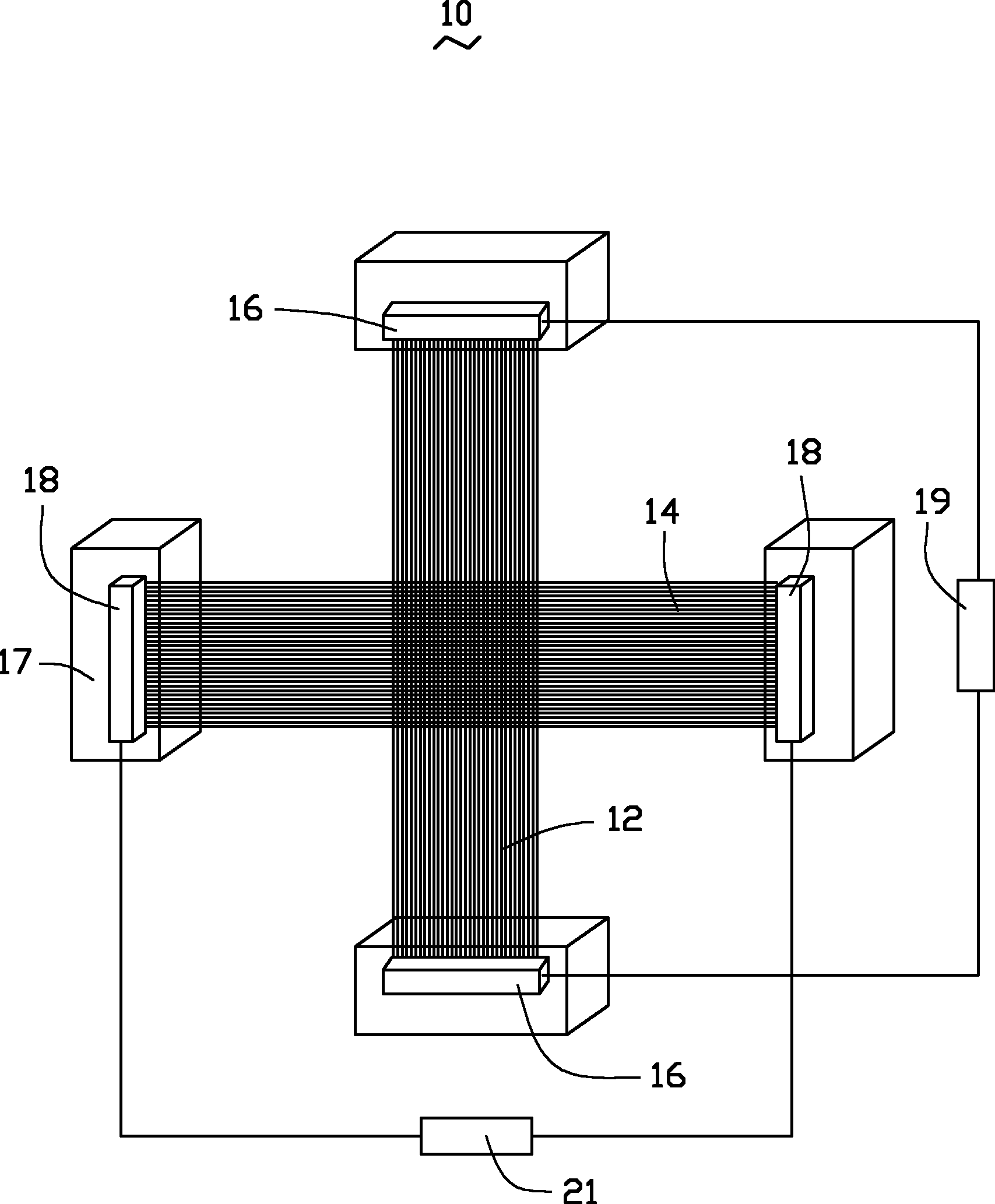
请参阅图1,本发明第一实施例提供一种电磁波检测装置10,其包括:一第一碳纳米管结构12,一第二碳纳米管结构14,两个第一电极16,及两个第二电极18。该第一碳纳米管结构12和第二碳纳米管结构14相对且间隔设置,所述第一碳纳米管结构12包括多个沿第一方向排列的碳纳米管,所述第二碳纳米管结构14包括多个沿第二方向排列的碳纳米管,且该第一方向基本垂直于该第二方向。该两个第一电极16相互间隔且分别与该第一碳纳米管结构12电连接,从一个第一电极16至另一个第一电极16的方向为该第一方向。该两个第二电极18相互间隔且分别与该第二碳纳米管结构12电连接,从一个第二电极18至另一个第二电极18的方向为该第二方向。所述电磁波检测装置10在使用时,待测的电磁波的入射方向优选为垂直于该第一碳纳米管结构12和第二碳纳米管结构14所在的平面,该第一碳纳米管结构12和第二碳纳米管结构14设置在该电磁波的传播路线上,该待测电磁波依次入射至该第一碳纳米管结构12及第二碳纳米管结构14。Please refer to Fig. 1, the first embodiment of the present invention provides an electromagnetic
所谓沿同一方向(第一方向或第二方向)排列是指多数碳纳米管的排列方向基本平行于该方向,如基本沿该方向择优取向排列。所谓择优取向是指大多数碳纳米管的整体延伸方向基本为该方向。而且,所述大多数碳纳米管的整体延伸方向基本平行于该碳纳米管结构的表面。当然,所述第一、第二碳纳米管结构12、14中存在少数随机排列的碳纳米管,这些碳纳米管不会对第一、第二碳纳米管结构12、14中大多数碳纳米管的整体取向排列构成明显影响。所述碳纳米管包括单壁碳纳米管、双壁碳纳米管及多壁碳纳米管中的一种或多种。所述单壁碳纳米管的直径为0.5纳米~10纳米,双壁碳纳米管的直径为1.0纳米~15纳米,多壁碳纳米管的直径为1.5纳米~50纳米。The so-called arrangement along the same direction (the first direction or the second direction) means that the arrangement direction of most carbon nanotubes is basically parallel to the direction, such as the preferential orientation arrangement basically along the direction. The so-called preferred orientation means that the overall extension direction of most carbon nanotubes is basically this direction. Moreover, the overall extension direction of the majority of carbon nanotubes is substantially parallel to the surface of the carbon nanotube structure. Of course, there are a small number of randomly arranged carbon nanotubes in the first and second
具体地,所述第一、第二碳纳米管结构12、14的整体形状为片状,可包括至少一碳纳米管膜、至少一碳纳米管线状结构或其组合。Specifically, the overall shape of the first and second
所述碳纳米管膜包括碳纳米管拉膜、带状碳纳米管膜或长碳纳米管膜。The carbon nanotube film includes a carbon nanotube drawn film, a ribbon carbon nanotube film or a long carbon nanotube film.
所述碳纳米管拉膜通过拉取一碳纳米管阵列直接获得,优选为通过拉取一超顺排碳纳米管阵列直接获得。该碳纳米管拉膜中的碳纳米管首尾相连地沿同一个方向择优取向排列,且为一自支撑结构,所述自支撑为碳纳米管拉膜不需要大面积的载体支撑,而只要相对两边提供支撑力即能整体上悬空而保持自身膜状状态,即将该碳纳米管拉膜置于(或固定于)间隔一定距离设置的两个支撑体上时,位于两个支撑体之间的碳纳米管拉膜能够悬空保持自身膜状状态。所述自支撑主要通过碳纳米管拉膜中存在连续的通过范德华力首尾相连延伸排列的碳纳米管而实现。请参阅图2及图3,具体地,每一碳纳米管拉膜包括多个连续且定向排列的碳纳米管片段143,该多个碳纳米管片段143通过范德华力首尾相连,每一碳纳米管片段143包括多个大致相互平行的碳纳米管145,该多个相互平行的碳纳米管145通过范德华力紧密结合。该碳纳米管片段143具有任意的宽度、厚度、均匀性及形状。所述碳纳米管拉膜的厚度为0.5纳米~100微米。所述碳纳米管拉膜及其制备方法请参见范守善等人于2007年2月9日申请的,于2008年8月13公开的第CN101239712A号中国大陆公开专利申请。The carbon nanotube drawn film is directly obtained by drawing a carbon nanotube array, preferably directly obtained by drawing a super-aligned carbon nanotube array. The carbon nanotubes in the carbon nanotube drawn film are arranged end-to-end along the same direction, and are a self-supporting structure. The self-supporting carbon nanotube drawn film does not need a large-area carrier support, but only relatively The supporting force provided by both sides means that it can be suspended in the air as a whole and maintain its own film state, that is, when the carbon nanotube stretched film is placed (or fixed) on two supports arranged at a certain distance, the space between the two supports The carbon nanotube stretched film can be suspended in the air to maintain its own film state. The self-supporting is mainly realized by the presence of continuous carbon nanotubes arranged end-to-end by van der Waals force in the carbon nanotube stretched film. Please refer to Fig. 2 and Fig. 3, specifically, each carbon nanotube stretched film includes a plurality of continuous and aligned carbon nanotube segments 143, and the plurality of carbon nanotube segments 143 are connected end to end by van der Waals force, and each carbon nanotube The tube segment 143 includes a plurality of carbon nanotubes 145 substantially parallel to each other, and the plurality of parallel carbon nanotubes 145 are closely combined by van der Waals force. The carbon nanotube segment 143 has any width, thickness, uniformity and shape. The thickness of the carbon nanotube drawn film is 0.5 nanometers to 100 micrometers. For the carbon nanotube drawn film and its preparation method, please refer to the Chinese mainland patent application No. CN101239712A filed on February 9, 2007 by Fan Shoushan et al. and published on August 13, 2008.
所述带状碳纳米管膜为通过将一狭长的碳纳米管阵列沿垂直于碳纳米管阵列长度方向倾倒在一基底表面而获得。该带状碳纳米管膜包括多个择优取向排列的碳纳米管。所述多个碳纳米管之间基本互相平行并排排列,且通过范德华力紧密结合,该多个碳纳米管具有大致相等的长度,且其长度可达到毫米量级。所述带状碳纳米管膜的宽度与碳纳米管的长度相等,故该带状碳纳米管阵列中至少有一个碳纳米管从带状碳纳米管膜的一端延伸至另一端,从而跨越整个带状碳纳米管膜。带状碳纳米管膜的宽度受碳纳米管的长度限制,优选地,该碳纳米管的长度为1毫米~10毫米。该所述带状碳纳米管膜的结构及其制备方法请参见范守善等人于2008年5月28日申请的第200810067529.X号中国大陆专利申请。The strip-shaped carbon nanotube film is obtained by pouring a long and narrow carbon nanotube array on the surface of a substrate along a direction perpendicular to the length of the carbon nanotube array. The ribbon-shaped carbon nanotube film includes a plurality of carbon nanotubes arranged in preferred orientations. The plurality of carbon nanotubes are basically arranged parallel to each other, and are tightly combined by van der Waals force. The plurality of carbon nanotubes have approximately equal lengths, and the lengths can reach the order of millimeters. The width of the ribbon-shaped carbon nanotube film is equal to the length of the carbon nanotube, so at least one carbon nanotube in the ribbon-shaped carbon nanotube array extends from one end of the ribbon-shaped carbon nanotube film to the other end, thus spanning the entire Ribbon carbon nanotube film. The width of the strip-shaped carbon nanotube film is limited by the length of the carbon nanotubes. Preferably, the length of the carbon nanotubes is 1 mm to 10 mm. For the structure and preparation method of the strip-shaped carbon nanotube film, please refer to the Chinese mainland patent application No. 200810067529.X filed on May 28, 2008 by Fan Shoushan et al.
所述长碳纳米管膜为通过放风筝法获得,具体为,使碳纳米管沿着碳源气体的气流方向生长,当停止通入碳源气体之后,该沿气流方向形成的超长碳纳米管将平行且间隔地倾倒至一接受基底上构成一长碳纳米管膜。该长碳纳米管膜包括多个平行于碳纳米管膜表面的超长碳纳米管,且该多个碳纳米管彼此基本平行排列。所述多个碳纳米管的长度可大于10厘米。所述碳纳米管膜中相邻两个超长碳纳米管之间的距离小于5微米。所述长碳纳米管膜的结构及其制备方法请参见范守善等人于2008年2月1日申请的第200810066048.7号中国大陆专利申请。The long carbon nanotube film is obtained by the kite-flying method, specifically, the carbon nanotubes are grown along the gas flow direction of the carbon source gas, and when the carbon source gas is stopped, the ultra-long carbon nanotubes formed along the gas flow direction The tubes will be poured parallel and spaced onto a receiving substrate to form a long carbon nanotube film. The long carbon nanotube film includes a plurality of ultra-long carbon nanotubes parallel to the surface of the carbon nanotube film, and the plurality of carbon nanotubes are arranged substantially parallel to each other. The length of the plurality of carbon nanotubes may be greater than 10 centimeters. The distance between two adjacent ultra-long carbon nanotubes in the carbon nanotube film is less than 5 microns. For the structure and preparation method of the long carbon nanotube film, please refer to the Chinese mainland patent application No. 200810066048.7 filed on February 1, 2008 by Fan Shoushan et al.
上述碳纳米管拉膜、带状碳纳米管膜或长碳纳米管膜为多个时,可共面且无间隙铺设或/和层叠铺设,从而制备不同面积与厚度的第一、第二碳纳米管结构12、14。在由多个共面且无间隙铺设和/或相互层叠的碳纳米管膜组成的碳纳米管结构中,相邻两个碳纳米管膜中的碳纳米管的排列方向相同。When there are multiple carbon nanotube films, strip-shaped carbon nanotube films or long carbon nanotube films, they can be laid coplanarly and without gaps or/and stacked to prepare first and second carbon nanotubes with different areas and thicknesses. Nanotube structures12,14. In a carbon nanotube structure composed of multiple coplanar carbon nanotube films laid and/or stacked with each other without gaps, the arrangement directions of the carbon nanotubes in two adjacent carbon nanotube films are the same.
所述碳纳米管线状结构包括至少一碳纳米管线。当该碳纳米管线状结构包括多个碳纳米管线时,该多个碳纳米管线可相互平行组成束状结构或相互扭转组成绞线结构。该碳纳米管线可以为非扭转的碳纳米管线或扭转的碳纳米管线。所述碳纳米管线状结构可为单根或多根。请参阅图4,当为单根时,该单根碳纳米管线状结构可在一平面内有序弯折成一膜状结构,且除弯折部分之外,该碳纳米管线状结构其它部分可看作并排且相互平行排列;请参阅图5,当为多根时,该多根碳纳米管线状结构可共面且沿一个方向平行排列或堆叠且沿一个方向平行排列设置。The carbon nanotube wire structure includes at least one carbon nanotube wire. When the carbon nanotube wire structure includes a plurality of carbon nanotube wires, the plurality of carbon nanotube wires can be parallel to each other to form a bundle structure or twisted to form a strand structure. The carbon nanotube wire can be a non-twisted carbon nanotube wire or a twisted carbon nanotube wire. The carbon nanotube linear structure can be single or multiple. Please refer to Figure 4, when it is single, the single carbon nanotube linear structure can be orderly bent into a film-like structure in a plane, and except for the bent part, other parts of the carbon nanotube linear structure can be Considered as being arranged side by side and parallel to each other; please refer to Figure 5, when there are multiple carbon nanotube linear structures, the multiple carbon nanotube linear structures can be coplanar and arranged in parallel along one direction or stacked and arranged in parallel along one direction.
所述非扭转的碳纳米管线包括多个沿该非扭转的碳纳米管线长度方向排列的碳纳米管。具体地,该非扭转的碳纳米管线包括多个碳纳米管片段,该多个碳纳米管片段通过范德华力首尾相连,每一碳纳米管片段包括多个相互平行并通过范德华力紧密结合的碳纳米管。该碳纳米管片段具有任意的长度、厚度、均匀性及形状。该非扭转的碳纳米管线长度不限,直径为0.5纳米~100微米。该非扭转的碳纳米管线为将碳纳米管拉膜通过有机溶剂处理得到。具体地,将有机溶剂浸润所述碳纳米管拉膜的整个表面,在挥发性有机溶剂挥发时产生的表面张力的作用下,碳纳米管拉膜中的相互平行的多个碳纳米管通过范德华力紧密结合,从而使碳纳米管拉膜收缩为一非扭转的碳纳米管线。该有机溶剂为挥发性有机溶剂,如乙醇、甲醇、丙酮、二氯乙烷或氯仿,本实施例中采用乙醇。通过有机溶剂处理的非扭转碳纳米管线与未经有机溶剂处理的碳纳米管膜相比,比表面积减小,粘性降低。The non-twisted carbon nanotube wire includes a plurality of carbon nanotubes arranged along the length direction of the non-twisted carbon nanotube wire. Specifically, the non-twisted carbon nanotube wire includes a plurality of carbon nanotube segments, the plurality of carbon nanotube segments are connected end to end by van der Waals force, and each carbon nanotube segment includes a plurality of carbon nanotube segments that are parallel to each other and closely combined by van der Waals force. nanotube. The carbon nanotube segment has any length, thickness, uniformity and shape. The length of the non-twisted carbon nanotubes is not limited, and the diameter is 0.5 nanometers to 100 microns. The non-twisted carbon nanotube wire is obtained by treating a drawn carbon nanotube film with an organic solvent. Specifically, the organic solvent is soaked into the entire surface of the carbon nanotube film, and under the action of the surface tension generated when the volatile organic solvent volatilizes, a plurality of carbon nanotubes in the carbon nanotube film that are parallel to each other pass through the van der Waals film. The force is closely combined, so that the carbon nanotube film shrinks into a non-twisted carbon nanotube wire. The organic solvent is a volatile organic solvent, such as ethanol, methanol, acetone, dichloroethane or chloroform, and ethanol is used in this embodiment. Compared with the carbon nanotube film without organic solvent treatment, the non-twisted carbon nanotube wire treated by organic solvent has a smaller specific surface area and lower viscosity.
所述扭转的碳纳米管线包括多个绕该扭转的碳纳米管线轴向螺旋排列并沿线的一端向另一端延伸的碳纳米管。具体地,该扭转的碳纳米管线包括多个碳纳米管片段,该多个碳纳米管片段通过范德华力首尾相连,每一碳纳米管片段包括多个相互平行并通过范德华力紧密结合的碳纳米管。该碳纳米管片段具有任意的长度、厚度、均匀性及形状。该扭转的碳纳米管线长度不限,直径为0.5纳米~100微米。所述扭转的碳纳米管线为采用一机械力将所述碳纳米管拉膜两端沿相反方向扭转获得。进一步地,可采用一挥发性有机溶剂处理该扭转的碳纳米管线。在挥发性有机溶剂挥发时产生的表面张力的作用下,处理后的扭转的碳纳米管线中相邻的碳纳米管通过范德华力紧密结合,使扭转的碳纳米管线的比表面积减小,密度及强度增大。The twisted carbon nanotube wire includes a plurality of carbon nanotubes arranged helically around the twisted carbon nanotube wire axially and extending from one end to the other end of the wire. Specifically, the twisted carbon nanotube wire includes a plurality of carbon nanotube segments, the plurality of carbon nanotube segments are connected end to end by van der Waals force, and each carbon nanotube segment includes a plurality of carbon nanotubes that are parallel to each other and closely combined by van der Waals force. Tube. The carbon nanotube segment has any length, thickness, uniformity and shape. The length of the twisted carbon nanotubes is not limited, and the diameter is 0.5 nanometers to 100 microns. The twisted carbon nanotube wire is obtained by using a mechanical force to twist the two ends of the carbon nanotube film in opposite directions. Further, the twisted carbon nanotubes can be treated with a volatile organic solvent. Under the action of the surface tension generated when the volatile organic solvent volatilizes, the adjacent carbon nanotubes in the treated twisted carbon nanotubes are closely combined by van der Waals force, so that the specific surface area of the twisted carbon nanotubes is reduced, and the density and Increased strength.
所述碳纳米管线状结构及其制备方法请参见范守善等人于2002年9月16日申请的,于2008年8月20日公告的第CN100411979C号中国大陆公告专利,以及范守善等人于2005年12月16日申请的,于2007年6月20日公开的第CN1982209A号中国大陆公开专利申请。For the linear structure of carbon nanotubes and the preparation method thereof, please refer to the CN100411979C patent issued by Fan Shoushan et al. on September 16, 2002 and announced on August 20, 2008, and the patent issued by Fan Shoushan et al. in 2005. Applied on December 16th, the Chinese mainland published patent application No. CN1982209A published on June 20, 2007.
该碳纳米管线状结构具有较大的强度,从而提高了该电磁波检测装置10的使用寿命和稳定性。The carbon nanotube linear structure has greater strength, thereby improving the service life and stability of the electromagnetic
若所述第一、第二碳纳米管结构12、14为碳纳米管膜或碳纳米管线状结构的组合时,所述碳纳米管膜中碳纳米管与碳纳米管线状结构沿相同方向排列。If the first and second
可以理解,上述碳纳米管结构均包括多个基本沿相同方向平行排列的碳纳米管、至少一个碳纳米管线状结构或其组合。该碳纳米管结构不限于上述列举的各种形式的纯的碳纳米管膜及碳纳米管线状结构,只要碳纳米管结构包括的碳纳米管基本沿同一方向排列,均在本发明保护的范围内。如,该碳纳米管结构还可为含有其他复合材料的碳纳米管复合膜及碳纳米管复合线状结构,其中所述复合材料为透光性有机聚合物,该有机聚合物可为聚甲基丙烯酸甲酯、聚碳酸酯、聚丙烯酸乙酯或聚丙烯酸丁酯等。It can be understood that the above-mentioned carbon nanotube structures all include a plurality of carbon nanotubes arranged in parallel substantially along the same direction, at least one carbon nanotube linear structure or a combination thereof. The carbon nanotube structure is not limited to the various forms of pure carbon nanotube films and carbon nanotube linear structures listed above, as long as the carbon nanotubes included in the carbon nanotube structure are basically arranged in the same direction, it is within the protection scope of the present invention Inside. For example, the carbon nanotube structure can also be a carbon nanotube composite film and a carbon nanotube composite linear structure containing other composite materials, wherein the composite material is a light-transmitting organic polymer, and the organic polymer can be polyformaldehyde. methyl acrylate, polycarbonate, polyethyl acrylate or polybutyl acrylate, etc.
由于碳纳米管对电磁波的吸收接近绝对黑体,从而使碳纳米管对于各种波长的电磁波具有均一的吸收特性,即该碳纳米管结构可测量红外线、可见光、紫外线等不同波长范围的电磁波。进一步地,碳纳米管在吸收了如激光等电磁波的能量后温度上升,从而使碳纳米管结构的电阻也相应发生了变化,该碳纳米管结构可以检测从微瓦到千瓦的电磁波强度范围。另外,由于碳纳米管具有较小的热容和较大的散热面积,因此,其对电磁波的响应速度也较快。因此,该碳纳米管结构可用于检测电磁波的强度变化。Since the absorption of electromagnetic waves by carbon nanotubes is close to that of an absolute black body, carbon nanotubes have uniform absorption characteristics for electromagnetic waves of various wavelengths, that is, the carbon nanotube structure can measure electromagnetic waves of different wavelength ranges such as infrared rays, visible light, and ultraviolet rays. Furthermore, the temperature of carbon nanotubes rises after absorbing the energy of electromagnetic waves such as lasers, so that the resistance of the carbon nanotube structure also changes accordingly. The carbon nanotube structure can detect electromagnetic wave intensities ranging from microwatts to kilowatts. In addition, since carbon nanotubes have a smaller heat capacity and a larger heat dissipation area, their response speed to electromagnetic waves is also faster. Therefore, the carbon nanotube structure can be used to detect intensity changes of electromagnetic waves.
另外,由于所述第一、第二碳纳米管结构12、14包括的多个碳纳米管、碳纳米管线状结构或其组合均沿同一方向平行排列,因此,当一电磁波信号首先入射至第一碳纳米管结构12时,振动方向平行于碳纳米管长度方向(第一方向)的电磁波信号被吸收,垂直于碳纳米管长度方向的电磁波信号能透过该第一碳纳米管结构12,使原电磁波信号变为偏振方向垂直于第一方向的偏振电磁波信号。由于该第一碳纳米管结构12吸收了偏振方向平行于碳纳米管长度方向的部分电磁波,因此该第一碳纳米管结构12的温度上升,且电阻发生相应改变。之后,该偏振方向垂直于第一方向的偏振电磁波信号入射至第二碳纳米管结构14。由于第二碳纳米管结构14中的多个碳纳米管与第一碳纳米管结构12中的多个碳纳米管相互垂直设置,即第二碳纳米管结构14中的碳纳米管的长度方向(第二方向)垂直于第一碳纳米管结构12中的碳纳米管的长度方向(第一方向),因此,该偏振方向垂直于第一方向的偏振电磁波信号被吸收,且第二碳纳米管结构12的温度升高,电阻也相应发生改变。可见,该第一碳纳米管结构12和第二碳纳米管结构14可分别吸收入射电磁波中两个偏振方向相互垂直的电磁波,且均会因吸收电磁波而引起温度升高,并导致电阻的改变。该第一碳纳米管结构12电阻的改变可被连接于第一电极16的第一信号检测装置19检测。该第二碳纳米管结构14电阻的改变可被连接于第二电极18的第二信号检测装置21检测。In addition, since the first and second
请参阅图6至图8,其中,图6中的R(300K)指该第一碳纳米管结构12或第二碳纳米管结构14在温度为300K时的电阻,R(T)指该第一碳纳米管结构12或第二碳纳米管结构14在不同温度T时的电阻,图7和图8中的Rdark指第一碳纳米管结构12或第二碳纳米管结构14未被电磁波照射时的电阻,RIR指第一碳纳米管结构12或第二碳纳米管结构14被电磁波照射时的电阻。从该图6至图8可以发现,该电阻的变化规律具体为该第一、第二碳纳米管结构12、14对电磁波的吸收越强烈,该第一、第二碳纳米管结构12、14的温度越高,其电阻越小;相反,该第一、第二碳纳米管结构12、14对电磁波的吸收越微弱,该第一、第二碳纳米管结构12、14的温度越低,其电阻越大。根据该电阻变化规律,该第一、第二碳纳米管结构12、14可以检测电磁波的强度。可见,该第一、第二碳纳米管结构12、14不仅可使入射电磁波发生偏振,还可以同时通过自身电阻的变化检测被吸收的具有一定偏振方向的电磁波的强度,因此,相比于传统的电磁波检测装置,该电磁波检测装置10无需额外的光敏元件,体积较小且成本较低。Please refer to FIG. 6 to FIG. 8, wherein R (300K) in FIG. 6 refers to the resistance of the first
另外,上述第一、第二碳纳米管结构12、14的厚度不宜太厚,太厚则使整个第一、第二碳纳米管结构12、14的单位面积热容增大,从而使该第一、第二碳纳米管结构12、14相应于入射电磁波的照射而引起的电阻变化所需反应时间较长,有可能降低该电磁波检测装置的灵敏度与稳定性。另外,该第一、第二碳纳米管结构12、14的厚度越小,单位面积热容越小,且整个电磁波检测装置10的灵敏度越高。该第一、第二碳纳米管结构12、14的单位面积热容可小于2×10⁻⁴焦耳每平方厘米开尔文,优选地,该单位面积热容小于1.7×10⁻⁶焦耳每平方厘米开尔文。但若其厚度太薄则也会使该第一、第二碳纳米管结构12、14的强度变差,在探测过程中容易损坏,影响该电磁波检测装置10的使用寿命。优选地,所述第一、第二碳纳米管结构12、14的厚度为0.5纳米~1毫米。本实施例中,所述第一、第二碳纳米管结构12、14均由15层相互层叠的碳纳米管拉膜组成。In addition, the thickness of the above-mentioned first and second
所述两个第一电极16和两个第二电极18由导电材料形成,具体为,该第一电极16和第二电极18的材料可选择为金属、导电聚合物、导电胶、金属性碳纳米管、铟锡氧化物等。该两个第一电极16和两个第二电极18的具体形状结构不限,具体地,该第一电极16和第二电极18可选择为层状、棒状、块状或其它形状。本实施例中,所述两个第一电极16为相互平行且间隔地设置于所述第一碳纳米管结构12的表面的块状铜电极,其中,所述第一碳纳米管结构12中的碳纳米管沿一第一电极16向另一第一电极16延伸。所述两个第二电极18也为相互平行且间隔地设置于所述第二碳纳米管结构14的表面的块状铜电极,其中,所述第二碳纳米管结构14中的碳纳米管沿其中一第二电极18向另一第二电极18延伸。由于碳纳米管具有极大的比表面积,在范德华力的作用下,该第一、第二碳纳米管结构12、14本身有很好的粘附性,故所述两个第一电极16和两个第二电极18可分别与所述第一碳纳米管结构16和第二碳纳米管结构18之间直接粘附固定,并形成很好的电接触。另外,也可以采用导电粘结层分别将所述两个第一电极16固定于第一碳纳米管结构12的表面,将两个第二电极18固定于第二碳纳米管结构14的表面。The two
此外,所述电磁波检测装置10进一步包括一用于支撑所述第一碳纳米管结构12和第二碳纳米管结构14的支撑体17。该支撑体17的形状不限,仅需使该第一、第二碳纳米管结构12、14相互间隔并悬空设置即可。所述支撑体17的材料为绝热材料,如玻璃、陶瓷等。本实施例中,该支撑体17由四个长方体形状的陶瓷元件组成。其中两个陶瓷元件分别支撑所述第一碳纳米管结构12的两端,具体为使该第一碳纳米管结构12的两端分别设置于该两个陶瓷元件的表面,即,该第一碳纳米管结构12的两端分别通过所述第一电极16和陶瓷元件夹持;另外两个陶瓷元件分别支撑所述第二碳纳米管结构14的两端,具体为使该第二碳纳米管结构14两端分别设置于该两个陶瓷元件的表面,即该第二碳纳米管结构14两端分别通过所述第二电极18和陶瓷元件夹持。该两对支撑体17具有不同的高度,从而使第一、第二碳纳米管结构12,14相互间隔。In addition, the electromagnetic
进一步地,为了定量的测定电磁波两个不同偏振方向的强度,可设置一与所述两个第一电极16电连接的第一信号测量装置19;同时,可进一步设置一与所述两个第二电极18电连接的第二信号测量装置21。该第一信号测量装置19和第二信号测量装置21可以为一电流测量装置或电压测量装置,本实施例中所述的第一信号测量装置19和第二信号测量装置21均为一电流测量装置。Further, in order to quantitatively measure the intensity of two different polarization directions of electromagnetic waves, a first
在应用中,采用所述电磁波检测装置10测量电磁波信号两个不同偏振方向的强度的方法为:S1,测量所述第一、第二碳纳米管结构12、14在未被电磁波照射时的电阻值Rdark;S2,在相同的条件下用多个强度已知且不同的电磁波分别照射所述第一、第二碳纳米管结构12、14,同时测得用该具有不同强度的电磁波照射该第一、第二碳纳米管结构12、14时,该第一、第二碳纳米管结构12、14的电阻变化率(Rdark-RIR)/Rdark,其中RIR为该第一、第二碳纳米管结构12、14被电磁波照射时的电阻值,从而拟合出一条第一、第二碳纳米管结构12、14的电阻变化率与入射电磁波强度之间的关系曲线;S3,在该相同的条件下用一待测的电磁波信号照射该电磁波检测装置10,用所述第一信号测量装置19和第二信号测量装置21分别测出此时第一、第二碳纳米管结构12、14的电阻变化率,根据上述已拟合出的第一、第二碳纳米管结构12、14的电阻变化率与入射电磁波强度之间的关系曲线,即可推出该待测电磁波两个不同偏振方向的强度。In application, the method of using the electromagnetic wave detection device 10 to measure the intensity of two different polarization directions of the electromagnetic wave signal is: S1, measure the resistance of the first and second carbon nanotube structures 12, 14 when they are not irradiated by electromagnetic waves value R dark ; S2, under the same condition, irradiate the first and second carbon nanotube structures 12, 14 with a plurality of electromagnetic waves with known and different intensities respectively, and at the same time measure that the electromagnetic waves with different intensities irradiate the For the first and second carbon nanotube structures 12 and 14, the resistance change rate (R dark -R IR )/R dark of the first and second carbon nanotube structures 12 and 14, wherein R IR is the first and second carbon nanotube structures 12 and 14 The resistance value of the second carbon nanotube structure 12, 14 when it is irradiated by electromagnetic waves, thereby fitting out a relationship curve between the resistance change rate of the first and second carbon nanotube structures 12, 14 and the intensity of the incident electromagnetic wave; S3, Under the same conditions, irradiate the electromagnetic wave detection device 10 with an electromagnetic wave signal to be measured, and measure the first and second carbon nanotube structures at this time with the first signal measuring device 19 and the second signal measuring device 21 respectively. The resistance change rate of 12,14, according to the relationship curve between the resistance change rate of the above-mentioned first and second
在上述步骤S1和S2中,由于本实施例所述第一碳纳米管结构12和第二碳纳米管结构14相同,均由15层的碳纳米管拉膜构成,因此仅需拟合出一条碳纳米管结构的电阻变化率(Rdark-RIR)/Rdark随入射电磁波的强度变化关系曲线即可。请参阅图7,本实施例在真空和非真空环境下分别拟合出了两条碳纳米管结构的电阻变化率同入射电磁波的强度之间的关系曲线。从图中可以发现,在真空环境下该第一、第二碳纳米管结构12、14对电磁波的响应较在非真空环境下的响应更灵敏。In the above-mentioned steps S1 and S2, since the first
在上述S3步骤中,所述待测电磁波直接照射该第一碳纳米管结构12,此时,该电磁波中偏振方向与该第一碳纳米管结构12中的碳纳米管长度方向相同的电磁波被吸收,而电磁波中偏振方向与碳纳米管长度方向垂直的电磁波则透过,因而,该第一碳纳米管结构12因吸收了部分电磁波而发生电阻变化;另外,所述透过第一碳纳米管结构12的电磁波则会照射到第二碳纳米管结构14上,由于该第二碳纳米管结构14中的碳纳米管排列方向与第一碳纳米管结构14中碳纳米管的排列方向相互垂直,因此,入射至其上的电磁波的偏振方向与该第二碳纳米管结构14中的碳纳米管排列方向相同,且被该第二碳纳米管结构14吸收,从而引起该第二碳纳米管结构14的电阻也发生变化。通过测量该第一碳纳米管结构12和第二碳纳米管结构14的电阻变化率即可同时获得该上述待测电磁波两个不同偏振方向的强度。In the above S3 step, the electromagnetic wave to be measured directly irradiates the first
请参阅图9,本发明第二实施例提供一种电磁波检测装置20,其包括多个按行和列排布的电磁波检测单元200。该每个电磁波检测单元200包括一第一碳纳米管结构22,一第二碳纳米管结构24,两个第一电极26,及两个第二电极28。该第一碳纳米管结构22和第二碳纳米管结构24相对并间隔设置,所述第一碳纳米管结构22包括多个沿第一方向排列的碳纳米管,所述第二碳纳米管结构24包括多个沿第二方向排列的碳纳米管,且该第一方向基本垂直于该第二方向。该两个第一电极26相互间隔且分别与该第一碳纳米管结构22电连接,从一个第一电极26至另一个第一电极26的方向为该第一方向。该两个第二电极28相互间隔且分别与该第二碳纳米管结构24电连接,从一个第二电极28至另一个第二电极28的方向为该第二方向。进一步地,该每个电磁波检测单元22还可包括用于支撑所述第一碳纳米管结构22和第二碳纳米管结构24的支撑体27。Referring to FIG. 9 , the second embodiment of the present invention provides an electromagnetic
本实施例与第一实施例基本相同,其区别在于本实施例的电磁波检测装置20为由多个阵列排布的电磁波检测单元200组成,且每个电磁波检测单元200与上述第一实施例的电磁波检测装置10的结构相同。This embodiment is basically the same as the first embodiment, the difference is that the electromagnetic
该多个电磁波检测单元200可以具有各自的第一方向及第二方向,不同的电磁波检测单元200的第一方向可以相同或不同,只要使每个电磁波检测单元200内部的第一方向基本垂直于第二方向即可。即仅需使每个电磁波检测单元200中的第一碳纳米管结构22中的多个碳纳米管排列方向基本垂直于第二碳纳米管结构22中的多个碳纳米管排列方向即可。当不同的电磁波检测单元200中的多个第一碳纳米管结构22中的碳纳米管排列方向不同,且有一相同的电磁波分别照射该多个电磁波检测单元200时,该多个电磁波检测单元200可同时检测该电磁波多个不同偏振方向的强度。其具体的检测原理及检测方法与第一实施例相同,在此不再赘述。The plurality of electromagnetic
该多个电磁波检测单元200中的多个第一电极26和多个第二电极28的设置方式不限。本实施例中,该电磁波检测装置20进一步包括多个第一导电条260和多个第二导电条280,该每个第一导电条260包括两个相互平行且间隔设置的第一导电线2600,该每个第二导电条280包括两个相互平行且间隔设置的第二导电线2800。该多个第一导电条260相互平行且间隔设置,该多个第二导电条280相互平行且间隔设置,且该多个第一导电条260和多个第二导电条280相互正交设置,从而形成多个按行和列排列的矩形网格,且在该第一导电条260和第二导电条280相互交叉的位置采用一绝缘片(图未示)间隔,以避免该第一导电条260和第二导电条280因电接触而发生短路。所述多个电磁波检测单元200一一对应的设置在该多个网格中,从而形成阵列结构。该每个第一导电条260中的一第一导电线2600与相邻一行的每个电磁波检测单元200的一第一电极26电连接,该另一第一导电线2600与相邻的另一行的每个电磁波检测单元200的一第二电极28电连接,同时,该每个第二导电条280中的一第二导电线2800与相邻一列的每个电磁波检测单元200的另一第一电极26电连接,该另一第二导电线2800与相邻的另一列的多个电磁波检测单元200的另一第二电极28电连接。可见,该每个电磁波检测单元200中的两个第一电极26分别与一第一导电线2600和一第二导电线2800电连接,两个第二电极28分别与另一第一导电线和另一第二导电线2800电连接。该与第一电极26电连接的第一导电线2600和与第二电极28电连接的第一导电线2600相邻且通过该电磁波检测单元200间隔,该与第一电极26电连接的第二导电线2800和与第二电极电连接的第二导电线2800相邻且通过该电磁波检测单元200间隔。该多个第一导电条260和多个第二导电条280的设置目的为便于该多个电磁波检测单元200与外部控制电路电连接。The arrangement of the plurality of first electrodes 26 and the plurality of
由于该电磁波检测装置20包括多个阵列排布的电磁波检测单元200,且每个电磁波检测单元200中均包括两个第一、第二碳纳米管结构22、24,该第一、第二碳纳米管结构22、24中的碳纳米管还可感测红外线,因此该电磁波检测装置20还可用于红外偏振成像。Since the electromagnetic
另外,本领域技术人员还可在本发明精神内做其他变化,当然,这些依据本发明精神所做的变化,都应包含在本发明所要求保护的范围之内。In addition, those skilled in the art can also make other changes within the spirit of the present invention. Of course, these changes made according to the spirit of the present invention should be included within the scope of protection claimed by the present invention.
Claims (19)
Priority Applications (2)
| Application Number | Priority Date | Filing Date | Title |
|---|---|---|---|
| CN201010209989.9A CN101881659B (en) | 2010-06-25 | 2010-06-25 | Electromagnetic wave detector |
| US12/964,005 US8305566B2 (en) | 2010-06-25 | 2010-12-09 | Apparatus for detecting electromagnetic waves |
Applications Claiming Priority (1)
| Application Number | Priority Date | Filing Date | Title |
|---|---|---|---|
| CN201010209989.9A CN101881659B (en) | 2010-06-25 | 2010-06-25 | Electromagnetic wave detector |
Publications (2)
| Publication Number | Publication Date |
|---|---|
| CN101881659A true CN101881659A (en) | 2010-11-10 |
| CN101881659B CN101881659B (en) | 2013-07-31 |
Family
ID=43053729
Family Applications (1)
| Application Number | Title | Priority Date | Filing Date |
|---|---|---|---|
| CN201010209989.9A Active CN101881659B (en) | 2010-06-25 | 2010-06-25 | Electromagnetic wave detector |
Country Status (2)
| Country | Link |
|---|---|
| US (1) | US8305566B2 (en) |
| CN (1) | CN101881659B (en) |
Cited By (1)
| Publication number | Priority date | Publication date | Assignee | Title |
|---|---|---|---|---|
| CN102065592A (en) * | 2010-11-23 | 2011-05-18 | 清华大学 | Micro heating device |
Families Citing this family (2)
| Publication number | Priority date | Publication date | Assignee | Title |
|---|---|---|---|---|
| CN104183785B (en) * | 2014-06-27 | 2016-05-11 | 京东方科技集团股份有限公司 | A kind of method for packing, OLED display floater and OLED display unit of OLED device |
| US11092623B2 (en) | 2018-12-11 | 2021-08-17 | Electronics And Telecommunications Research Institute | Current sensor for measuring alternating electromagnetic wave and a current breaker using the same |
Citations (4)
| Publication number | Priority date | Publication date | Assignee | Title |
|---|---|---|---|---|
| US20080170982A1 (en) * | 2004-11-09 | 2008-07-17 | Board Of Regents, The University Of Texas System | Fabrication and Application of Nanofiber Ribbons and Sheets and Twisted and Non-Twisted Nanofiber Yarns |
| CN101610613A (en) * | 2008-06-18 | 2009-12-23 | 清华大学 | Line heat source |
| US20100039015A1 (en) * | 2007-12-29 | 2010-02-18 | Tsinghua University | Thermionic emission device |
| US20100122980A1 (en) * | 2008-06-13 | 2010-05-20 | Tsinghua University | Carbon nanotube heater |
Family Cites Families (7)
| Publication number | Priority date | Publication date | Assignee | Title |
|---|---|---|---|---|
| CN100411979C (en) | 2002-09-16 | 2008-08-20 | 清华大学 | A carbon nanotube rope and its manufacturing method |
| CN100500556C (en) | 2005-12-16 | 2009-06-17 | 清华大学 | Carbon nano-tube filament and its production |
| CN101497436B (en) | 2008-02-01 | 2015-06-03 | 清华大学 | Carbon nano-tube thin-film structure and preparation method thereof |
| CN101591015B (en) | 2008-05-28 | 2013-02-13 | 清华大学 | Preparation method of banded carbon nano tube film |
| US20100126985A1 (en) | 2008-06-13 | 2010-05-27 | Tsinghua University | Carbon nanotube heater |
| CN101846549B (en) * | 2009-03-25 | 2011-12-14 | 清华大学 | Electromagnetic wave detection device and detection method |
| WO2011148425A1 (en) * | 2010-05-27 | 2011-12-01 | パナソニック株式会社 | Thermoelectric conversion device, radiation detector, and radiation detection method using same |
-
2010
- 2010-06-25 CN CN201010209989.9A patent/CN101881659B/en active Active
- 2010-12-09 US US12/964,005 patent/US8305566B2/en active Active
Patent Citations (4)
| Publication number | Priority date | Publication date | Assignee | Title |
|---|---|---|---|---|
| US20080170982A1 (en) * | 2004-11-09 | 2008-07-17 | Board Of Regents, The University Of Texas System | Fabrication and Application of Nanofiber Ribbons and Sheets and Twisted and Non-Twisted Nanofiber Yarns |
| US20100039015A1 (en) * | 2007-12-29 | 2010-02-18 | Tsinghua University | Thermionic emission device |
| US20100122980A1 (en) * | 2008-06-13 | 2010-05-20 | Tsinghua University | Carbon nanotube heater |
| CN101610613A (en) * | 2008-06-18 | 2009-12-23 | 清华大学 | Line heat source |
Cited By (3)
| Publication number | Priority date | Publication date | Assignee | Title |
|---|---|---|---|---|
| US8492682B2 (en) | 2010-11-22 | 2013-07-23 | Tsinghua University | Micro heater |
| CN102065592A (en) * | 2010-11-23 | 2011-05-18 | 清华大学 | Micro heating device |
| CN102065592B (en) * | 2010-11-23 | 2013-03-20 | 清华大学 | Micro heating device |
Also Published As
| Publication number | Publication date |
|---|---|
| US8305566B2 (en) | 2012-11-06 |
| US20110317155A1 (en) | 2011-12-29 |
| CN101881659B (en) | 2013-07-31 |
Similar Documents
| Publication | Publication Date | Title |
|---|---|---|
| CN101846549B (en) | Electromagnetic wave detection device and detection method | |
| CN101893659B (en) | Method and device for detecting polarization direction of electromagnetic wave | |
| CN101848564B (en) | Heating element | |
| US8811632B2 (en) | Thermoacoustic device | |
| CN101459019B (en) | Thermal electron source | |
| CN101819335B (en) | Thermochromatic element and thermochromatic display device | |
| TWI429296B (en) | speaker | |
| CN101871818A (en) | Infrared detector | |
| CN101894903B (en) | Photoelectric conversion device | |
| CN102056065A (en) | Sound production device | |
| CN101881659B (en) | Electromagnetic wave detector | |
| CN101626639A (en) | Plane heat source | |
| CN107726971A (en) | Strain transducer | |
| US8081287B2 (en) | Liquid crystal display with carbon nanotube heating element | |
| TWI615599B (en) | Device and method for detecting light wavelength | |
| CN101771922B (en) | Sounding device | |
| TWI397701B (en) | Device and method for detecting electromagnetic wave | |
| CN101610613B (en) | Line heat source | |
| CN103841506B (en) | The preparation method of thermophone array | |
| TWI414797B (en) | Electromagnetic wave detecting device | |
| CN101636004A (en) | Plane heat source | |
| CN103841504B (en) | Thermophone array | |
| TWI400436B (en) | Method and device for measuring a polarizing direction of an electromagnetic wave | |
| CN103901247B (en) | Potential difference measurements method | |
| TW201736809A (en) | Image sensor |
Legal Events
| Date | Code | Title | Description |
|---|---|---|---|
| C06 | Publication | ||
| PB01 | Publication | ||
| C10 | Entry into substantive examination | ||
| SE01 | Entry into force of request for substantive examination | ||
| C14 | Grant of patent or utility model | ||
| GR01 | Patent grant |