CN101860252B - Three-level converter for optimizing device overcurrent protection and enlarging system safety operation area - Google Patents
Three-level converter for optimizing device overcurrent protection and enlarging system safety operation area Download PDFInfo
- Publication number
- CN101860252B CN101860252B CN201010162953XA CN201010162953A CN101860252B CN 101860252 B CN101860252 B CN 101860252B CN 201010162953X A CN201010162953X A CN 201010162953XA CN 201010162953 A CN201010162953 A CN 201010162953A CN 101860252 B CN101860252 B CN 101860252B
- Authority
- CN
- China
- Prior art keywords
- switching device
- converter
- overcurrent protection
- phase
- current
- Prior art date
- Legal status (The legal status is an assumption and is not a legal conclusion. Google has not performed a legal analysis and makes no representation as to the accuracy of the status listed.)
- Expired - Fee Related
Links
Images


Landscapes
- Inverter Devices (AREA)
- Dc-Dc Converters (AREA)
Abstract
优化器件过流保护扩大系统安全运行区的三电平变换器属于电力电子变换器技术领域,其特征在于:将常规具有器件过流保护功能的驱动电路用于三电平变换器,针对位于变换器不同拓扑位置开关器件的驱动电路,进行过流保护参数相互关联的合理设置,从而避免驱动过流保护动作时发生单个器件承受全边直流母线电压的现象,保证开关器件及变换器的安全、正常工作。本发明依据开关器件特性、变换器换流过程来确定过流保护的阈值,充分利用开关器件的关断电流能力,扩大变换器系统安全运行区域,同时不需要改变变换器的控制系统,具有易于实现、可靠性高的优点。
The three-level converter that optimizes device over-current protection and expands the safe operating area of the system belongs to the technical field of power electronic converters, and is characterized in that: the conventional drive circuit with device over-current protection function is used for the three-level converter, and is aimed at the conversion The driving circuits of switching devices in different topological positions of the switch, and reasonably set the over-current protection parameters related to each other, so as to avoid the phenomenon that a single device bears the full-side DC bus voltage when driving the over-current protection action, and ensure the safety of switching devices and converters. normal work. The present invention determines the threshold value of the overcurrent protection according to the characteristics of the switching device and the commutation process of the converter, fully utilizes the ability of the switching device to shut off the current, and expands the safe operation area of the converter system, and does not need to change the control system of the converter at the same time. The advantages of realization and high reliability.
Description
技术领域 technical field
本发明属于电力电子应用技术领域,适用于基于电力电子开关器件IGBT、IGCT或MOSFET等的三电平变换器,避免单个开关器件驱动过流保护直接用于变换器发生器件承受全边直流母线电压等现象,保证开关器件及变换器的安全、正常工作。The invention belongs to the technical field of power electronics application, is applicable to a three-level converter based on power electronic switching devices such as IGBT, IGCT or MOSFET, and avoids driving overcurrent protection of a single switching device to be directly used in the converter generating device to withstand full-side DC bus voltage and other phenomena to ensure the safety and normal operation of switching devices and converters.
背景技术 Background technique
目前,电力电子变换器应用范围非常广泛,可以覆盖到发电、输电、储电和用电的所有应用领域,成为例如电机变频调速节能、电能质量控制、高品质电源、新能源发电等应用的基础,但由于电力电子器件的水平有限,开关速度和容量存在矛盾,所以高性能的开关器件和变换器拓扑综合考虑成为一种理想解决办法。近10年来,三电平变换器得到快速的发展,如用于电力系统电能质量控制的基于高压IGBT的三电平变换器、用于高压高性能变频调速的基于IGCT的三电平变换器、用于高效率新能源并网发电的基于MOSFET的三电平变换器等。这类变换器的优点之一是,主电路中的每个开关器件只承受一半的直流母线电压,可充分利用器件的电压等级,无需动态均压电路。At present, the application range of power electronic converters is very wide, covering all application fields of power generation, power transmission, power storage and power consumption. However, due to the limited level of power electronic devices, there is a contradiction between switching speed and capacity, so the comprehensive consideration of high-performance switching devices and converter topology has become an ideal solution. In the past 10 years, three-level converters have developed rapidly, such as high-voltage IGBT-based three-level converters for power system power quality control, and IGCT-based three-level converters for high-voltage high-performance frequency control. , MOSFET-based three-level converters for high-efficiency new energy grid-connected power generation, etc. One of the advantages of this type of converter is that each switching device in the main circuit only bears half of the DC bus voltage, which can fully utilize the voltage level of the device without a dynamic voltage equalization circuit.
但是,将传统的两电平变换器所使用的单个开关器件驱动过流保护直接用于该类变换器中,在某些特定条件下,将破坏上述的优点,甚至直接造成开关器件损坏。在传统的两电平变换器所使用的驱动电路中,其过流保护功能只考虑所驱动器件本身,不需要考虑与其他器件的关系。而在三电平变换器中,变换器拓扑不再像两电平电路那样具有完美的对称性,变换器中存在“内管”和“外管”之分,两者之间的开关动作存在关联,流经“外管”的电流一定要流经“内管”,这种拓扑上的关联,决定了传统的独立开关器件驱动过流保护直接使用将存在破坏变换器安全运行的风险,本发明正是通过一种优化器件过流保护解决该问题,并依据参数的选择来扩大变换器安全运行区,实现优化器件过流保护扩大系统安全运行区的三电平变换器。However, directly applying the single switching device drive overcurrent protection used in traditional two-level converters to this type of converter will destroy the above advantages and even directly cause damage to the switching device under certain specific conditions. In the driving circuit used in the traditional two-level converter, its overcurrent protection function only considers the driven device itself, and does not need to consider the relationship with other devices. In the three-level converter, the converter topology no longer has the perfect symmetry like the two-level circuit. There are "inner tube" and "outer tube" in the converter, and the switching action between the two exists Correlation, the current flowing through the "outer tube" must flow through the "inner tube". This topological correlation determines that the direct use of traditional independent switching devices to drive over-current protection will have the risk of destroying the safe operation of the converter. The invention solves this problem through an optimized device over-current protection, and expands the safe operation area of the converter according to the selection of parameters to realize a three-level converter that optimizes the device over-current protection and expands the system's safe operation area.
发明内容Contents of the invention
本发明的目的在于扩大三电平变换器的系统运行区。The object of the present invention is to enlarge the system operating area of a three-level converter.
本发明的特征在于,The present invention is characterized in that,
在任何相,上半臂由第一开关器件(TX1)和第二开关器件(TX2)IGBT模块串联而成,下半臂由第三开关器件(TX3)和第四开关器件(TX4)IGBT模块串联而成。In any phase, the upper half arm is composed of the first switching device (T X1 ) and the second switching device (T X2 ) IGBT modules connected in series, and the lower half arm is composed of the third switching device (T X3 ) and the fourth switching device (T X4 ) IGBT modules are connected in series.
所述第二开关器件(TX2)的发射极和第三开关器件(TX3)的集电极相连,构成输出端。The emitter of the second switching device (T X2 ) is connected to the collector of the third switching device (T X3 ), forming an output terminal.
在所述第四开关器件(TX4)和第三开关器件(TX3)的串接点到第二开关器件(TX2)和第一开关器件(TX1)的串接点之间依次正向串接有两个箝位二极管。Between the series connection point of the fourth switching device (T X4 ) and the third switching device (T X3 ) to the series connection point of the second switching device (T X2 ) and the first switching device (T X1 ) There are two clamping diodes connected.
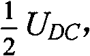
在所述第二开关器件(TX2)的发射极和第一开关器件(TX1)的集电极之间,在所述第四开关器件(TX4)的发射极和第三开关器件(TX3)的集电极之间,各输入半边直流母线电压 Between the emitter of the second switching device (T X2 ) and the collector of the first switching device (T X1 ), between the emitter of the fourth switching device (T X4 ) and the third switching device (T Between the collectors of X3 ), each half of the input DC bus voltage
在所述各开关器件(TX1、TX2、TX3、TX4)的栅极分别输入一个由外部驱动电路输入的PWM驱动信号。A PWM driving signal input by an external driving circuit is respectively input to the gates of the switching devices (T X1 , T X2 , T X3 , T X4 ).
所述第二开关器件(TX2)和第三开关器件(TX3)对应的所述驱动电路的过流保护阈值设置为IIN,而IIN=k1IC,其中,IC为所述第二开关器件(TX2)和第三开关器件(TX3)最大可关断电流值,0.8≤k1≤0.95。The overcurrent protection threshold of the drive circuit corresponding to the second switching device (T X2 ) and the third switching device (T X3 ) is set to I IN , and I IN =k 1 IC , where IC is the The maximum turn-off current values of the second switch device (T X2 ) and the third switch device (T X3 ) are 0.8≤k 1 ≤0.95.
所述第一开关器件(TX1)和第四开关器件(TX4)对应的所述驱动电路的过流保护阈值设置为IEX,而IEX=k2IIN,0.9≤k2≤0.95。The overcurrent protection threshold of the drive circuit corresponding to the first switching device (T X1 ) and the fourth switching device (T X4 ) is set to I EX , and I EX =k 2 I IN , 0.9≤k 2 ≤0.95 .
所述X为U、V、W各相的代码,The X is the code of each phase of U, V, W,
对于U相,所述X=U,For phase U, the X=U,
对于V相,所述X=V,For V phase, the X=V,
对于W相,所述X=W。For the W phase, the X=W.
本发明的效果是避免单个开关器件驱动过流保护动作时,发生器件承受全边直流母线电压现象,保证开关器件及变换器的安全、正常工作,并可以调整相应系数来扩大变换器系统安全运行区。The effect of the present invention is to avoid the phenomenon that the device bears the full-side DC bus voltage when a single switching device drives the overcurrent protection action, ensure the safety and normal operation of the switching device and the converter, and can adjust the corresponding coefficients to expand the safe operation of the converter system district.
附图说明Description of drawings
图1.本发明系统结构示意图;Fig. 1. Schematic diagram of system structure of the present invention;
图2.单个开关承受全边母线电压现象的情况之一及采用本发明器件过流保护的情况;Figure 2. One of the situations where a single switch bears the full-side bus voltage phenomenon and the situation of using the device overcurrent protection of the present invention;
图3.单个开关承受全边母线电压现象的情况之二及采用本发明器件过流保护的情况。Fig. 3. The second case where a single switch bears the full-side bus voltage phenomenon and the case of using the device overcurrent protection of the present invention.
具体实施方式 Detailed ways
本发明是一种优化器件过流保护扩大系统安全运行区的三电平变换器,适用于基于电力电子开关器件IGBT、IGCT或MOSFET等变换器。将常规单个开关器件的驱动电路用于变换器时,通过不同拓扑位置的开关器件驱动过流保护参数相关联的合理设置,从而避免单个开关器件驱动过流保护动作时发生器件承受全边直流母线电压的现象,保证开关器件及变换器的安全、正常工作。本发明依据开关器件特性、变换器换流过程来确定过流保护的阈值,充分利用开关器件的关断电流能力,扩大变换器系统安全运行区,同时不需要改变变换器的控制系统,具有易于实现、可靠性高的优点。基于IGBT的变换器拓扑如图1所示(基于IGCT和MOSFET等器件的电路在此不赘述),其中驱动电路从变换器的控制系统接收12路PWM驱动脉冲,向12个开关器件(IGBT或者IGCT、MOSFET)发出12路PWM驱动信号,每路驱动电路能够检测对应开关器件电流状态,当流过器件的电流达到设定阈值时能够主动关闭对应的开关器件,即每个驱动电路是能对单个器件进行过流保护的常规驱动电路。The invention is a three-level converter which optimizes device overcurrent protection and expands the safe operation area of the system, and is suitable for converters based on power electronic switching devices such as IGBT, IGCT or MOSFET. When the drive circuit of a conventional single switching device is used in the converter, the switching devices in different topological positions are used to drive the reasonable settings associated with the overcurrent protection parameters, so as to avoid the device from being subjected to the full-side DC bus when the single switching device drives the overcurrent protection action Voltage phenomenon, to ensure the safety and normal operation of switching devices and converters. The present invention determines the threshold value of the overcurrent protection according to the characteristics of the switching device and the commutation process of the converter, fully utilizes the ability of the switching device to shut off the current, and expands the safe operation area of the converter system, and does not need to change the control system of the converter at the same time. The advantages of realization and high reliability. The IGBT-based converter topology is shown in Figure 1 (circuits based on IGCT and MOSFET devices are not described here), in which the drive circuit receives 12 PWM drive pulses from the control system of the converter, and supplies 12 switching devices (IGBT or IGCT, MOSFET) send out 12 channels of PWM drive signals, each drive circuit can detect the current state of the corresponding switching device, and when the current flowing through the device reaches the set threshold, it can actively turn off the corresponding switching device, that is, each drive circuit can control Conventional drive circuit for overcurrent protection of a single device.
则本发明按照以下步骤实现的器件过流保护:Then the device overcurrent protection that the present invention realizes according to the following steps:
步骤1:根据12个开关器件的用户手册,确定开关器件的最大可关断电流值为IC,一般的12个开关器件为相同型号,其最大可关断电流能力是器件的最主要性能,是器件标识的主要参数,如1200伏600安的IGBT,指的就是在一定温度条件下,其最大可关断电流为600A;Step 1: According to the user manuals of the 12 switching devices, determine the maximum turn-off current value I C of the switching devices. Generally, the 12 switching devices are of the same type, and their maximum turn-off current capability is the most important performance of the device. It is the main parameter of device identification, such as 1200V 600A IGBT, which means that under certain temperature conditions, its maximum turn-off current is 600A;
步骤2:将图1所示的变换器中的“内管”,即TU2、TU3、TV2、TV3、TW2和TW3这6只开关器件对应的驱动电路的过流保护阈值设置相同,均为IIN,而IIN=k1IC,其中0.8≤k1≤0.95,考虑驱动电路检测到过流与开关器件关断动作完成之间存在时间延迟,在该延迟内,器件中的电流仍在增大,为保证器件安全关断,其过流保护设定值IIN要比器件最大可关断电流IC小,系数k1越接近1,对驱动电路要求越高;Step 2: Set the "inner tube" in the converter shown in Figure 1, that is, the six switching devices T U2 , T U3 , T V2 , T V3 , T W2 and T W3 to the overcurrent protection threshold of the drive circuit corresponding to The settings are the same, both are I IN , and I IN =k 1 I C , where 0.8≤k 1 ≤0.95, considering that there is a time delay between the drive circuit detecting overcurrent and the completion of the switching device’s turn-off action, within this delay, The current in the device is still increasing. In order to ensure the safe shutdown of the device, its overcurrent protection setting value I IN should be smaller than the maximum shutdown current I C of the device. The closer the coefficient k 1 is to 1, the higher the requirements for the driving circuit ;
步骤3:将变换器中的“外管”,即TU1、TU4、TV1、TV4、TW1和TW4这6只开关器件对应的驱动电路的过流保护阈值设置相同,均为IEX,而IEX=k2IIN,其中0.9≤k2≤0.95,外管对应的驱动电路过流保护阈值要比内管的小,即内管和外管中流经相同电流,该电流在不断增加的过程中,保证外管先进行过流保护关断动作,否则可能发生内管承受全边直流母线电压的现象,考虑到各驱动电路参数设置的分散性,内管和外管的过流保护阈值之间有一定的差距,用系数k2表示,其越接近1,对驱动电路的参数设置的准确度要求越高,在使用相同开关器件条件下,k1·k2越接近1,系统可输出的最大电流越大,变换器系统安全运行区域越大。Step 3: Set the "outer tube" in the converter, that is, the overcurrent protection thresholds of the drive circuits corresponding to the six switching devices T U1 , T U4 , T V1 , T V4 , T W1 and T W4 to be the same, all of which are I EX , and I EX =k 2 I IN , where 0.9≤k 2 ≤0.95, the overcurrent protection threshold of the drive circuit corresponding to the outer tube is smaller than that of the inner tube, that is, the same current flows through the inner tube and the outer tube, and the current is In the process of continuous increase, ensure that the outer tube performs the over-current protection shut-off action first, otherwise the phenomenon that the inner tube may bear the full-side DC bus voltage may occur. Considering the dispersion of the parameter settings of each drive circuit, the over-current There is a certain gap between the current protection thresholds, expressed by the coefficient k 2 , the closer it is to 1, the higher the accuracy of the parameter setting of the drive circuit is, and the closer k 1 k 2 is to 1 under the condition of using the same switching device , the larger the maximum current that the system can output, the larger the safe operating area of the converter system.
上述步骤和关键参数确定具有以下特征:The above steps and determination of key parameters have the following characteristics:
1.变换器系统的最大可输出电流跟IC、k1和k2密切相关,其中IC为变换器中开关器件的最大可关断电流,k1为驱动电路保护动作带来的电流折算系数,k2为不同拓扑位置电流折算系数,k1和k2的合理选择,能够扩大系统安全运行区;1. The maximum output current of the converter system is closely related to I C , k 1 and k 2 , where I C is the maximum turn-off current of the switching device in the converter, and k 1 is the current conversion brought by the protection action of the drive circuit Coefficient, k 2 is the current conversion coefficient of different topological positions, reasonable selection of k 1 and k 2 can expand the safe operating area of the system;
2.内管和外管使用了不同的电流保护阈值,即使用了系数k2,保证了开关器件保护动作之间的相互关系,避免了过流保护动作时单个开关器件承受全边母线电压而造成损坏;2. The inner tube and the outer tube use different current protection thresholds, that is, the coefficient k 2 is used to ensure the mutual relationship between the protection actions of the switching devices, and to avoid the failure of a single switching device to bear the full-side bus voltage during the over-current protection action. cause damage;
3.除了脉冲信号,该方法不需要附加的变换器状态识别;3. In addition to the pulse signal, the method does not require additional converter state identification;
4.器件过流保护只在驱动电路中实现,不需要改变一般变换器的控制系统,实现简单,可靠性高。4. Device overcurrent protection is only implemented in the drive circuit, without changing the control system of the general converter, which is simple to implement and highly reliable.
通过分析可以证明本发明的中器件过流保护作用,为说明方便,采用“1”和“0”来表示开关器件驱动信号的状态,“1”表示让开关器件导通,“0”表示让开关器件阻断。Through analysis, it can be proved that the device overcurrent protection function of the present invention is convenient. For the convenience of explanation, "1" and "0" are used to represent the state of the switching device driving signal, "1" means to make the switching device conduct, and "0" means to let The switching device blocks.
图1是本发明系统结构示意图。Fig. 1 is a schematic diagram of the system structure of the present invention.
图2是单个开关承受全边母线电压现象情况之一及采用本发明器件过流保护的情况。对于变换器的一个桥臂,比如U相桥臂,当桥臂处于“1100”状态,即TU1、TU2导通,TU3、TU4阻断,如图中(a)所示,当流经开关器件的电流发生过流时,直接使用常规驱动电路并且TU1、TU2使用一样的过流保护阈值设置,存在以下两种情况:Fig. 2 is one of the situations where a single switch bears the full-side bus voltage and the situation where the device overcurrent protection of the present invention is adopted. For a bridge arm of the converter, such as the U-phase bridge arm, when the bridge arm is in the "1100" state, that is, T U1 and T U2 are on, and T U3 and T U4 are off, as shown in (a) in the figure, when When the current flowing through the switching device is over-current, the conventional drive circuit is used directly and T U1 and T U2 use the same over-current protection threshold setting, there are the following two situations:
1)由于驱动电路参数的发散性,有可能造成TU2的保护动作先执行,TU2关断,保护动作完成时则形成如图中(b)所示的情况,此时TU2将承受全边直流母线电压;1) Due to the divergence of the drive circuit parameters, it may cause the protection action of T U2 to be executed first, and T U2 is turned off. When the protection action is completed, the situation shown in (b) in the figure will be formed. At this time, T U2 will bear the full load. Side DC bus voltage;
2)即使TU1、TU2同时保护动作,保护动作完后形成如图中(d)所示情况,在(a)向(d)的动作中存在两器件同时动作,有一个器件承受大于半边直流母线电压的情况,同时输出电压存在全边直流母线电压的跳跃。2) Even if T U1 and T U2 are protected at the same time, the situation shown in (d) in the figure will be formed after the protection action is completed. In the action from (a) to (d), there are two devices that operate at the same time, and one device withstands more than half of the load. In the case of DC bus voltage, at the same time, the output voltage has a full-side DC bus voltage jump.
这两种情况都损失了三电平变换器的优点,甚至造成器件过压损坏。而在本发明中,确保了此时外管TU1先于内管TU2动作关断,形成如图中(c)所示的状态,如果电流继续增加触发TU2保护动作,或者由控制系统封锁所有脉冲,形成如图中(d)所示情况,在采用本发明的过流保护策略形成的(a)到(c)到(d)的过程中,无器件承受过压的现象,同时输出电压不存在全边直流母线电压的跳跃。In both cases, the advantages of the three-level converter are lost, and even the device is damaged due to overvoltage. In the present invention, it is ensured that the outer tube T U1 is turned off before the inner tube T U2 at this time, forming a state as shown in (c) in the figure. If the current continues to increase, the protection action of T U2 is triggered, or the control system All pulses are blocked to form the situation shown in (d) in the figure. In the process of (a) to (c) to (d) formed by the overcurrent protection strategy of the present invention, no device is subjected to overvoltage, and at the same time There is no jump in the output voltage of the full-side DC bus voltage.
图3是单个开关承受全边母线电压现象情况之二及采用本发明器件过流保护的情况。对于三电平变换器的一个桥臂,比如U相桥臂,当桥臂处于“0011”状态,即TU1、TU2阻断,TU3、TU4导通,如图中(a)所示。当流经开关器件的电流发生过流时,直接使用常规驱动电路并且TU3、TU4使用一样的过流保护阈值设置,同样存在可能使器件承受过压的两种情况,即从(a)到(b)或者(a)到(d)的情况,而在本发明中,器件过流保护形成的(a)到(c)到(d)的过程中,无器件承受过压的现象,详细分析与跟“1100”状态类似,不再赘述。Fig. 3 is the second situation of a single switch bearing the full-side bus voltage phenomenon and the situation of using the device overcurrent protection of the present invention. For a bridge arm of a three-level converter, such as the U-phase bridge arm, when the bridge arm is in the "0011" state, that is, T U1 and T U2 are blocked, and T U3 and T U4 are turned on, as shown in (a) in the figure Show. When the current flowing through the switching device is over-current, use the conventional drive circuit directly and use the same over-current protection threshold setting for T U3 and T U4 , and there are also two situations that may cause the device to withstand overvoltage, that is, from (a) In the case of (b) or (a) to (d), in the present invention, in the process of (a) to (c) to (d) formed by the device overcurrent protection, there is no phenomenon that the device is subjected to overvoltage, The detailed analysis is similar to the "1100" state, so I won't repeat it here.
虽然,在所有器件过流保护阈值设置为一样的方式中,不是每一台变换器每次保护动作都发生器件承受过压的情况,但其仍是一个巨大隐患,而在本发明中,优化的器件过流保护避免了这一情况。同时在本发明中,根据器件特性来确定IC,根据三电平不同的拓扑位置来确定内管和外管的过流保护阈值,使用了两个关键系数,k1为驱动电路保护动作带来的电流折算系数,k2为不同拓扑位置电流折算系数,k1和k2的合理选择,扩大了系统安全运行区。Although, in the way in which the overcurrent protection thresholds of all devices are set to be the same, not every converter will suffer from overvoltage every time the protection action occurs, but it is still a huge hidden danger, and in the present invention, the optimized The device overcurrent protection avoids this situation. At the same time, in the present invention, IC is determined according to the characteristics of the device, and the overcurrent protection thresholds of the inner tube and the outer tube are determined according to the different topological positions of the three levels. Two key coefficients are used, and k 1 is the driving circuit protection action band K 2 is the current conversion coefficient of different topological positions, and the reasonable selection of k 1 and k 2 expands the safe operation area of the system.
Claims (1)
Priority Applications (1)
| Application Number | Priority Date | Filing Date | Title |
|---|---|---|---|
| CN201010162953XA CN101860252B (en) | 2010-04-28 | 2010-04-28 | Three-level converter for optimizing device overcurrent protection and enlarging system safety operation area |
Applications Claiming Priority (1)
| Application Number | Priority Date | Filing Date | Title |
|---|---|---|---|
| CN201010162953XA CN101860252B (en) | 2010-04-28 | 2010-04-28 | Three-level converter for optimizing device overcurrent protection and enlarging system safety operation area |
Publications (2)
| Publication Number | Publication Date |
|---|---|
| CN101860252A CN101860252A (en) | 2010-10-13 |
| CN101860252B true CN101860252B (en) | 2012-07-18 |
Family
ID=42945950
Family Applications (1)
| Application Number | Title | Priority Date | Filing Date |
|---|---|---|---|
| CN201010162953XA Expired - Fee Related CN101860252B (en) | 2010-04-28 | 2010-04-28 | Three-level converter for optimizing device overcurrent protection and enlarging system safety operation area |
Country Status (1)
| Country | Link |
|---|---|
| CN (1) | CN101860252B (en) |
Families Citing this family (8)
| Publication number | Priority date | Publication date | Assignee | Title |
|---|---|---|---|---|
| US8730691B2 (en) * | 2011-05-11 | 2014-05-20 | Eaton Corporation | Power conversion apparatus and methods employing variable-level inverters |
| CN102427219B (en) * | 2011-10-11 | 2014-04-02 | 常州联力自动化科技有限公司 | Short circuit protection system and safe closing control method of three-level converter power tube |
| CN103001517B (en) * | 2012-11-14 | 2015-03-25 | 国网智能电网研究院 | Modular multi-level voltage source converter submodule device and control method thereof |
| CN104883084B (en) * | 2015-05-26 | 2017-10-03 | 清华大学 | A kind of neutral point clamp type cascaded H-bridges mixed multi-level current transformer |
| CN106452136B (en) * | 2016-06-20 | 2019-04-02 | 清华大学 | A multi-port power electronic converter for energy internet |
| CN106787872B (en) * | 2016-12-12 | 2019-06-04 | 全球能源互联网研究院有限公司 | A Method for Determining Safe Operating Areas of H-Bridge Modules and Cascaded Multilevel Converters |
| CN111239470A (en) * | 2019-12-27 | 2020-06-05 | 西安工程大学 | Method for monitoring current of IGBT module integrated shunt in real time |
| CN114421796A (en) * | 2021-12-31 | 2022-04-29 | 深圳市禾望科技有限公司 | I-type three-level topological overcurrent sealing wave control method |
Family Cites Families (5)
| Publication number | Priority date | Publication date | Assignee | Title |
|---|---|---|---|---|
| JP2005012913A (en) * | 2003-06-19 | 2005-01-13 | Hitachi Ltd | Power converter |
| GB0402319D0 (en) * | 2004-02-03 | 2004-03-10 | M & Fc Holdings Llc | Wide range power supply for polyphase electricity meter |
| CN100442620C (en) * | 2005-02-03 | 2008-12-10 | 昂宝电子(上海)有限公司 | Systems and methods for multi-threshold overcurrent protection of switching power converters |
| JP4438833B2 (en) * | 2007-07-04 | 2010-03-24 | トヨタ自動車株式会社 | Abnormality detection apparatus and abnormality detection method for power converter |
| CN101470142B (en) * | 2007-12-27 | 2011-03-09 | 英业达股份有限公司 | Overcurrent detection circuit, step-down converter and overcurrent detection method |
-
2010
- 2010-04-28 CN CN201010162953XA patent/CN101860252B/en not_active Expired - Fee Related
Also Published As
| Publication number | Publication date |
|---|---|
| CN101860252A (en) | 2010-10-13 |
Similar Documents
| Publication | Publication Date | Title |
|---|---|---|
| CN101860252B (en) | Three-level converter for optimizing device overcurrent protection and enlarging system safety operation area | |
| CN104009446B (en) | A kind of DC transmission protection device, transverter and guard method | |
| CN102237672B (en) | System and method for protection of a multilevel converter | |
| US10033378B2 (en) | Apparatus and method for solid state power control of current load | |
| EP2662968B1 (en) | Three-level inverter | |
| Li et al. | Novel hybrid DC/DC converter topology for HVDC interconnections | |
| CN110943615B (en) | A fault ride-through method for low-loss modular multilevel DC-DC converters | |
| CN103731059B (en) | A kind of two clamped sub-module structure circuit of modularization multi-level converter | |
| CN102931822B (en) | Main circuit pulse based active voltage-equalizing device for high voltage IGBTs (Insulated Gate Bipolar Transistors) in series connection | |
| CN110888085A (en) | Inverter short circuit detection method and device and inverter | |
| JPWO2014181450A1 (en) | Control device for insulated gate semiconductor element and power conversion device using the same | |
| US11632059B1 (en) | Submodule topology circuit for modular multilevel converter and method for controlling same | |
| CN110299696B (en) | T-shaped three-level converter and short-circuit protection circuit thereof | |
| CN105119511B (en) | A kind of MMC submodular circuits with DC side failure blocking ability | |
| CN110994560B (en) | A low-loss modular multilevel converter fault ride-through method | |
| Choudhury | Present status of SiC based power converters and gate drivers–a review | |
| CN104993716A (en) | Modular multilevel converter and hybrid double-unit sub-module | |
| Isik et al. | Fault-tolerant control and isolation method for NPC-based AFEC using series-connected 10kV SiC MOSFETs | |
| Ying et al. | High power conversion technologies & trend | |
| CN106712639B (en) | Vidacare corp and electrical equipment | |
| CN100391075C (en) | IGCT-based method for safely blocking pulses in medium and high voltage three-level converters | |
| CN110995039B (en) | A low-loss modular multilevel converter and its parameter design method | |
| Wikstroem et al. | A Technology Platform for Reverse-Conducting Integrated Gate Commutated Thyristors with 94 mm Device Diameter | |
| CN115065263A (en) | Three-level inverter, photovoltaic system and control method | |
| CN117013817A (en) | A buffer voltage equalizing circuit that can turn off the converter and the converter topology |
Legal Events
| Date | Code | Title | Description |
|---|---|---|---|
| C06 | Publication | ||
| PB01 | Publication | ||
| C10 | Entry into substantive examination | ||
| SE01 | Entry into force of request for substantive examination | ||
| C14 | Grant of patent or utility model | ||
| GR01 | Patent grant | ||
| CF01 | Termination of patent right due to non-payment of annual fee | ||
| CF01 | Termination of patent right due to non-payment of annual fee |
Granted publication date: 20120718 |