[go: up one dir, main page]

CN101840928B - Polysilicon Pillar Bipolar Transistor with Self-Aligned Memory Elements - Google Patents

Polysilicon Pillar Bipolar Transistor with Self-Aligned Memory Elements Download PDF

Info

Publication number
CN101840928B
CN101840928B CN201010108856.2A CN201010108856A CN101840928B CN 101840928 B CN101840928 B CN 101840928B CN 201010108856 A CN201010108856 A CN 201010108856A CN 101840928 B CN101840928 B CN 101840928B
Authority
CN
China
Prior art keywords
emitter
memory cells
doped polysilicon
forming
single crystal
Prior art date
Legal status (The legal status is an assumption and is not a legal conclusion. Google has not performed a legal analysis and makes no representation as to the accuracy of the status listed.)
Active
Application number
CN201010108856.2A
Other languages
Chinese (zh)
Other versions
CN101840928A (en
Inventor
龙翔澜
赖二琨
林仲汉
毕平拉詹德南
Current Assignee (The listed assignees may be inaccurate. Google has not performed a legal analysis and makes no representation or warranty as to the accuracy of the list.)
Macronix International Co Ltd
International Business Machines Corp
Original Assignee
Macronix International Co Ltd
International Business Machines Corp
Priority date (The priority date is an assumption and is not a legal conclusion. Google has not performed a legal analysis and makes no representation as to the accuracy of the date listed.)
Filing date
Publication date
Application filed by Macronix International Co Ltd, International Business Machines Corp filed Critical Macronix International Co Ltd
Publication of CN101840928A publication Critical patent/CN101840928A/en
Application granted granted Critical
Publication of CN101840928B publication Critical patent/CN101840928B/en
Active legal-status Critical Current
Anticipated expiration legal-status Critical

Links

Images

Classifications

    • HELECTRICITY
    • H10SEMICONDUCTOR DEVICES; ELECTRIC SOLID-STATE DEVICES NOT OTHERWISE PROVIDED FOR
    • H10BELECTRONIC MEMORY DEVICES
    • H10B63/00Resistance change memory devices, e.g. resistive RAM [ReRAM] devices
    • H10B63/30Resistance change memory devices, e.g. resistive RAM [ReRAM] devices comprising selection components having three or more electrodes, e.g. transistors
    • H10B63/32Resistance change memory devices, e.g. resistive RAM [ReRAM] devices comprising selection components having three or more electrodes, e.g. transistors of the bipolar type
    • HELECTRICITY
    • H10SEMICONDUCTOR DEVICES; ELECTRIC SOLID-STATE DEVICES NOT OTHERWISE PROVIDED FOR
    • H10BELECTRONIC MEMORY DEVICES
    • H10B69/00Erasable-and-programmable ROM [EPROM] devices not provided for in groups H10B41/00 - H10B63/00, e.g. ultraviolet erasable-and-programmable ROM [UVEPROM] devices
    • HELECTRICITY
    • H10SEMICONDUCTOR DEVICES; ELECTRIC SOLID-STATE DEVICES NOT OTHERWISE PROVIDED FOR
    • H10BELECTRONIC MEMORY DEVICES
    • H10B63/00Resistance change memory devices, e.g. resistive RAM [ReRAM] devices
    • H10B63/80Arrangements comprising multiple bistable or multi-stable switching components of the same type on a plane parallel to the substrate, e.g. cross-point arrays
    • HELECTRICITY
    • H10SEMICONDUCTOR DEVICES; ELECTRIC SOLID-STATE DEVICES NOT OTHERWISE PROVIDED FOR
    • H10NELECTRIC SOLID-STATE DEVICES NOT OTHERWISE PROVIDED FOR
    • H10N70/00Solid-state devices having no potential barriers, and specially adapted for rectifying, amplifying, oscillating or switching
    • H10N70/011Manufacture or treatment of multistable switching devices
    • H10N70/021Formation of switching materials, e.g. deposition of layers
    • H10N70/023Formation of switching materials, e.g. deposition of layers by chemical vapor deposition, e.g. MOCVD, ALD
    • HELECTRICITY
    • H10SEMICONDUCTOR DEVICES; ELECTRIC SOLID-STATE DEVICES NOT OTHERWISE PROVIDED FOR
    • H10NELECTRIC SOLID-STATE DEVICES NOT OTHERWISE PROVIDED FOR
    • H10N70/00Solid-state devices having no potential barriers, and specially adapted for rectifying, amplifying, oscillating or switching
    • H10N70/011Manufacture or treatment of multistable switching devices
    • H10N70/021Formation of switching materials, e.g. deposition of layers
    • H10N70/026Formation of switching materials, e.g. deposition of layers by physical vapor deposition, e.g. sputtering
    • HELECTRICITY
    • H10SEMICONDUCTOR DEVICES; ELECTRIC SOLID-STATE DEVICES NOT OTHERWISE PROVIDED FOR
    • H10NELECTRIC SOLID-STATE DEVICES NOT OTHERWISE PROVIDED FOR
    • H10N70/00Solid-state devices having no potential barriers, and specially adapted for rectifying, amplifying, oscillating or switching
    • H10N70/011Manufacture or treatment of multistable switching devices
    • H10N70/061Shaping switching materials
    • H10N70/066Shaping switching materials by filling of openings, e.g. damascene method
    • HELECTRICITY
    • H10SEMICONDUCTOR DEVICES; ELECTRIC SOLID-STATE DEVICES NOT OTHERWISE PROVIDED FOR
    • H10NELECTRIC SOLID-STATE DEVICES NOT OTHERWISE PROVIDED FOR
    • H10N70/00Solid-state devices having no potential barriers, and specially adapted for rectifying, amplifying, oscillating or switching
    • H10N70/20Multistable switching devices, e.g. memristors
    • H10N70/231Multistable switching devices, e.g. memristors based on solid-state phase change, e.g. between amorphous and crystalline phases, Ovshinsky effect
    • HELECTRICITY
    • H10SEMICONDUCTOR DEVICES; ELECTRIC SOLID-STATE DEVICES NOT OTHERWISE PROVIDED FOR
    • H10NELECTRIC SOLID-STATE DEVICES NOT OTHERWISE PROVIDED FOR
    • H10N70/00Solid-state devices having no potential barriers, and specially adapted for rectifying, amplifying, oscillating or switching
    • H10N70/20Multistable switching devices, e.g. memristors
    • H10N70/24Multistable switching devices, e.g. memristors based on migration or redistribution of ionic species, e.g. anions, vacancies
    • H10N70/245Multistable switching devices, e.g. memristors based on migration or redistribution of ionic species, e.g. anions, vacancies the species being metal cations, e.g. programmable metallization cells
    • HELECTRICITY
    • H10SEMICONDUCTOR DEVICES; ELECTRIC SOLID-STATE DEVICES NOT OTHERWISE PROVIDED FOR
    • H10NELECTRIC SOLID-STATE DEVICES NOT OTHERWISE PROVIDED FOR
    • H10N70/00Solid-state devices having no potential barriers, and specially adapted for rectifying, amplifying, oscillating or switching
    • H10N70/801Constructional details of multistable switching devices
    • H10N70/821Device geometry
    • H10N70/826Device geometry adapted for essentially vertical current flow, e.g. sandwich or pillar type devices
    • HELECTRICITY
    • H10SEMICONDUCTOR DEVICES; ELECTRIC SOLID-STATE DEVICES NOT OTHERWISE PROVIDED FOR
    • H10NELECTRIC SOLID-STATE DEVICES NOT OTHERWISE PROVIDED FOR
    • H10N70/00Solid-state devices having no potential barriers, and specially adapted for rectifying, amplifying, oscillating or switching
    • H10N70/801Constructional details of multistable switching devices
    • H10N70/821Device geometry
    • H10N70/828Current flow limiting means within the switching material region, e.g. constrictions
    • HELECTRICITY
    • H10SEMICONDUCTOR DEVICES; ELECTRIC SOLID-STATE DEVICES NOT OTHERWISE PROVIDED FOR
    • H10NELECTRIC SOLID-STATE DEVICES NOT OTHERWISE PROVIDED FOR
    • H10N70/00Solid-state devices having no potential barriers, and specially adapted for rectifying, amplifying, oscillating or switching
    • H10N70/801Constructional details of multistable switching devices
    • H10N70/881Switching materials
    • H10N70/882Compounds of sulfur, selenium or tellurium, e.g. chalcogenides
    • H10N70/8822Sulfides, e.g. CuS
    • HELECTRICITY
    • H10SEMICONDUCTOR DEVICES; ELECTRIC SOLID-STATE DEVICES NOT OTHERWISE PROVIDED FOR
    • H10NELECTRIC SOLID-STATE DEVICES NOT OTHERWISE PROVIDED FOR
    • H10N70/00Solid-state devices having no potential barriers, and specially adapted for rectifying, amplifying, oscillating or switching
    • H10N70/801Constructional details of multistable switching devices
    • H10N70/881Switching materials
    • H10N70/882Compounds of sulfur, selenium or tellurium, e.g. chalcogenides
    • H10N70/8828Tellurides, e.g. GeSbTe
    • HELECTRICITY
    • H10SEMICONDUCTOR DEVICES; ELECTRIC SOLID-STATE DEVICES NOT OTHERWISE PROVIDED FOR
    • H10NELECTRIC SOLID-STATE DEVICES NOT OTHERWISE PROVIDED FOR
    • H10N70/00Solid-state devices having no potential barriers, and specially adapted for rectifying, amplifying, oscillating or switching
    • H10N70/801Constructional details of multistable switching devices
    • H10N70/881Switching materials
    • H10N70/883Oxides or nitrides
    • H10N70/8833Binary metal oxides, e.g. TaOx
    • HELECTRICITY
    • H10SEMICONDUCTOR DEVICES; ELECTRIC SOLID-STATE DEVICES NOT OTHERWISE PROVIDED FOR
    • H10NELECTRIC SOLID-STATE DEVICES NOT OTHERWISE PROVIDED FOR
    • H10N70/00Solid-state devices having no potential barriers, and specially adapted for rectifying, amplifying, oscillating or switching
    • H10N70/801Constructional details of multistable switching devices
    • H10N70/881Switching materials
    • H10N70/883Oxides or nitrides
    • H10N70/8836Complex metal oxides, e.g. perovskites, spinels

Landscapes

  • Engineering & Computer Science (AREA)
  • Manufacturing & Machinery (AREA)
  • Chemical & Material Sciences (AREA)
  • Materials Engineering (AREA)
  • Semiconductor Memories (AREA)

Abstract

本发明提出一种具有自对准于双极接面晶体管存取装置的射极的存储元件的存储单元及此种装置的制造方法。在此所述的储存装置包括多个存储单元。在这些存储单元中的存储单元包含一包括射极的双极接面晶体管(BJT),该射极包括掺杂的多晶硅柱。这样的存储单元包含一个在射极上的绝缘元件,且绝缘元件具有一个延伸穿过绝缘层的开口,这个开口在射极上的中心。而这些存储单元还包含在开口中的一存储元件,且此一存储元件与上述射极电性相连。

Figure 201010108856

The present invention provides a memory cell having a memory element self-aligned to the emitter of a bipolar junction transistor access device and a method for manufacturing such a device. The memory device described herein includes a plurality of memory cells. The memory cell in these memory cells includes a bipolar junction transistor (BJT) including an emitter, wherein the emitter includes a doped polysilicon column. Such a memory cell includes an insulating element on the emitter, and the insulating element has an opening extending through the insulating layer, and the opening is centered on the emitter. These memory cells also include a memory element in the opening, and the memory element is electrically connected to the above-mentioned emitter.

Figure 201010108856

Description

The polysilicon pillar bipolar transistor that has the autoregistration memory element
Technical field
The invention relates to a kind of high density storage device (memory devices) that is the basis with phase-change storage material (phase change based memorymaterials); And phase-change storage material comprises chalcogenide material (chalcogenide based materials) and other programmable resistor material (programmable resistive material), and the method for making this device.
Background technology
Phase-change storage material such as chalcogenide material and materials similar can be suitable for being implemented in the electric current of the degree in the integrated circuit by supply, and cause the phase change between amorphous state and the crystalline state.General amorphous characteristics are to have the resistance value higher than general crystalline state (electrical resistivity), and this can be sensed in order to expression data (data) immediately.Such characteristic has caused the concern of using programmable resistor material to form non-volatile memory circuit, and this can random-accessly read and write.
Normally a kind of reduced-current operation of variation from the amorphous state to the crystalline state.And the normally a kind of high current from crystalline state to amorphous variation that is referred to herein as replacement (reset) is operated; It comprises the high current density pulse (pulse) of a weak point; So that fusing or interrupt crystalline texture; Rapid cooling phase-change material afterwards quenches the phase-change material that is melted and make the phase-change material of part at least stable in amorphous state.
Because phase change be since heating make right, so for heating phase-change material and lure required phase change into, need sizable electric current.Because the low relatively current drives of field-effect transistor, thereby on the required electric current of the phase change memory cell (cell) that obtains to have the field-effect transistor access device, have problems.
Though bipolar junction transistor can provide the current drives also bigger than field-effect transistor, the integration (integration) of bipolar junction transistor and CMOS peripheral circuit difficulty and possibly cause the design and craft of high complexity.
Phase change memory device size by reducing in the unit can reduce the amount of electric current, so that reach higher current density with the little absolute current value (absolute current values) through phase change memory device.Yet, have the device of very small dimensions and have problems at the device that manufacturing meets the required technologic variation of the franchise condition (tolerancerequirement) of the required strictness of large scale high density storage device (largescale high-density memory device) in manufacturing.
Therefore the phase-change memory cell with bipolar junction transistor access device need be provided, satisfy with the CMOS peripheral circuit in the design integration complexity and on identical integrated circuit, can be compatible with the manufacturing of peripheral circuit.And, the method for the phase-change memory cell of making the franchise condition satisfy the required strictness of large scale high density storage device need be provided.
Summary of the invention
Have in this description and to be self-aligned to bipolar junction transistor (bipolar junction transistor, BJT) memory cell of the memory element of the emitter-base bandgap grading of access device (element).A kind of storage device described here (device) comprises a plurality of memory cell.Memory cell in these memory cell comprises a bipolar junction transistor, and bipolar junction transistor comprises an emitter-base bandgap grading, and emitter-base bandgap grading comprises a DOPOS doped polycrystalline silicon post (pillar ofdoped polysilicon).One insulation component is arranged on emitter-base bandgap grading, and have an opening that extends through insulation component, this center on emitter-base bandgap grading, opening position.In opening, also have a memory element and emitter-base bandgap grading to be electrical connected.
Particularly, during forming sacrificial member, can form above-mentioned emitter-base bandgap grading, this sacrificial member is the position that is used for defining the memory element of follow-up formation.Remove sacrificial member afterwards,, and in above-mentioned interlayer hole, form insulation component with a definition interlayer hole (via) on emitter-base bandgap grading.Above-mentioned memory element is formed in one by in the defined opening of insulation component.Can be by this of an array that causes technology in the very little variation of the inferior photoetching width (sublithographic width) of memory element to form to cross memory cell by the defined opening of insulation component.
A memory cell described here causes the active region (active region) in the memory element that can done minimumly, reduces the amount (magnitude) of luring the electric current that phase change is required into thus.By the width of the memory element in the defined opening of insulation component less than the width of DOPOS doped polycrystalline silicon post and conductor lid (conductive cap) as emitter-base bandgap grading; Be preferably also forr a short time than the minimal characteristic length like photoetching process (feature size), above-mentioned technology is meant the technology that is used to form DOPOS doped polycrystalline silicon post, conductor lid and bit line.And little width can be concentrated the current density in the memory element, reduces the amount of the electric current of luring in the active region that phase change is required into thus.In addition, insulation component can provide some thermal insulations of active region (thermal isolation), lures the essential magnitude of current of phase change (amount ofcurrent) into to promote to reduce.And the remainder of memory element can be active region the thermal insulation with bit line is provided.
The method of a kind of manufacturing one storage device described here comprises forming to have a single crystal substrates (single-crystalline substrate) of one first conductive state.In single crystal substrates, form a plurality of dielectric irrigation canals and ditches (dielectric trenches) then, and in single crystal substrates, form a plurality of character lines.One of them the character line of dielectric irrigation canals and ditches space between adjacent of dielectric irrigation canals and ditches.Then, form a kind of structure in single crystal substrates, this structure comprises the doped polycrystalline silicon materials, at conductive cap material on the doped polycrystalline silicon materials and the expendable material on the conductive cap material (sacrificial material).Then, the patterning said structure is to form a plurality of laminations (stacks) on character line.Afterwards, on the sidewall of lamination, form a plurality of sidewall spacers (sidewall spacers).Then, remove expendable material, defining a plurality of interlayer holes (via), and in interlayer hole, form an insulating barrier, this insulating barrier defines a plurality of openings.Then, in opening, form a plurality of memory elements, and on memory element, form a plurality of bit lines.
In the embodiment described here, the memory cell that can be manufactured on the logic device of surrounding zone (peripheral region) simultaneously and have bipolar junction transistor in the memory block.In memory block and surrounding zone, form grid dielectric material earlier.Remove the grid dielectric material in the memory block then, and in memory block and surrounding zone, form one deck doped polycrystalline silicon materials and one deck conductive cap material.Afterwards, use doped polycrystalline silicon materials and conductive cap material to come to form together the grid of logic device and the emitter-base bandgap grading of bipolar junction transistor access device (access devices).As a result, storage device described here will comprise and have bipolar junction transistor access device phase-change memory cell (phase change memory cells) and CMOS peripheral circuit, and satisfy design and integrate the complexity (complexity) with technology.
Description of drawings
For letting the above-mentioned feature and advantage of the present invention can be more obviously understandable, hereinafter is special lifts embodiment, and conjunction with figs. elaborates as follows, wherein:
Fig. 1 is a kind of sketch map of borrowing the memory cell array of a part of using the memory cell realization with bipolar junction transistor (BJT) of being with polysilicon emitter-base bandgap grading and autoregistration memory element (self-aligned memory elements) described here.
Fig. 2 A and Fig. 2 B show the profile of the memory cell that is arranged in the part in the array, and Fig. 2 A is to be along character line along bit line and Fig. 2 B.
Fig. 3 A shows the profile of one second embodiment of the embodiment of similar Fig. 2 A~Fig. 2 B, and on the end face of the higher doped of bit line, a top conductor that comprises silicide is arranged.
Fig. 4~Figure 17 B shows a kind of step of production order of array of the memory cell of making the bipolar junction transistor with band polysilicon emitter-base bandgap grading and autoregistration memory element described here.
Figure 18~Figure 21 shows a kind of alternate embodiment to the formation character line that in Fig. 5 A~Fig. 5 B, shows.
Figure 22 is a kind of calcspar of simplification of integrated circuit, and aforementioned integrated circuit comprises a kind of memory cell array of borrowing the memory cell realization of using the bipolar junction transistor with band polysilicon emitter-base bandgap grading and autoregistration memory element described here.
Embodiment
The following description that this paper discloses is as representing ground about concrete structure embodiment and method.Should know that these are described not will be with the content constraints that discloses in these concrete embodiment and method that disclose, but can use further feature, element, method and embodiment to put into practice the content of exposure.Described preferred embodiment is in order to explain orally the present invention but not in order to limit its scope, should be as the criterion with the claim scope definition.Have common knowledge the knowledgeable in the affiliated technical field and should understand upward multiple equal change (variation) of description hereinafter.Element similar in each embodiment is usually with reference to similar component symbol.
Fig. 1 shows a kind of sketch map of borrowing the memory cell array 100 of a part of using the memory cell realization with bipolar junction transistor (BJT) of being with polysilicon emitter-base bandgap grading and autoregistration memory element (self-aligned memory elements) described here.
Shown in the sketch map of Fig. 1; Each memory cell of array 100 comprises a bipolar junction transistor access device and a memory element that is arranged in electrical series connection (electrical series), and described memory element can be configured to the data (data) that therefore can store one or more in the lump in a plurality of resistance states (resistive states).
Array 100 comprises a plurality of character lines 130, and it comprises character line 130a, 130b, 130c, 130d that parallel connection extends first direction and is electrical connected with wordline decoders/driver (decoder/driver) 150.Character line 130 is connected to the base terminal (baseterminals) of the bipolar access transistor of array 100.
A plurality of bit lines 120 parallel connections that comprise bit line 120a, 120b, 120c, 120d extend second direction and are electrical connected with bit line decoder 160.And the emitter-base bandgap grading end of each other bipolar junction transistor is connected to a corresponding bit line 120 via memory element.
The memory cell of array 100 connects into and collects utmost point configuration (common collectorconfiguration) altogether.In collecting utmost point configuration altogether, the collector terminal of memory cell is to be connected to a fixing reference voltage (reference voltage), and input and output are respectively base terminal and emitter-base bandgap grading end.Therefore, when operation in bit line 120 and the voltage on the character line 130 can respond to an electric current via emitter-base bandgap grading end and memory element from bit line 120 to collector terminal, perhaps vice versa.
In Fig. 1, collector terminal is linked ground wire (ground).Collector terminal also can select to be connected to a voltage source, to be supplied with not in a reference voltage of ground wire.Such as the bias arrangement supply voltage, the current and power supply (Biasing Arrangement Supply Voltages, Current Sources) 2236 that see also Figure 22.
Memory cell 110 is to represent the memory cell of array 100 and comprise the bipolar junction transistor 115 and phase change memory device 125 that is arranged as electrical series connection.The base terminal of bipolar junction transistor 115 is connected to character line 130b, and the emitter-base bandgap grading end of transistor 115 is connected to a 120b via phase change memory device 125.
Can to respond to an electric current, reach the memory cell 110 that reads or write array 100 by supplying suitable voltage and/or electric current to corresponding word line acts 130b and corresponding bit line 120b through selected memory cell 110.The position accurate (level) of the voltage/current of being supplied with the duration (duration) decide according to the operation of being implemented such as read operation or write operation.
In one of memory cell 110 is reset (wiping) operation; Supply a replacement pulse (reset pulse) to character line 130b and make bit line 120b via memory element 125 induction one electric current; Transformation (transition) with the active region that causes memory element 125 becomes an amorphous phase, thereby makes this phase-change material become the resistance of a resistance value in the scope of Reset Status.Described replacement pulse is a quite high energy pulse, and the temperature of active region at least that is enough to improve memory element 125 is above and also more than fusion temperature, active region is in liquid state so that let at least to transformation (crystallization) temperature of phase-change material.Stop rapidly described replacement pulse afterwards, cause a quickish cool time and active region is cooled to rapidly below the transition temperature, so that active region is stable to general amorphous phase.
Be provided with in (or programming) operation in one of memory cell 110; Supply a programming pulse to the amplitude that is fit to and the duration character line 130b and bit line 120b; To respond to an electric current via memory cell 110; This electric current is enough to improve the temperature of active region of at least a portion to more than the transition temperature and cause the active region of at least a portion to become crystalline phase from amorphous phase transition, and such transformation will reduce the resistance of memory element 125 and make memory cell 110 be in desired state.
One of data value in being stored in memory cell 110 reads in (or sensing) operation; Supply one read pulse to the amplitude that is fit to the duration corresponding word line acts 130b and corresponding bit line 120b, can not make memory element 125 experience the variation of resistance states (resistive state) with induced current flow.The electric current of the memory cell of flowing through 110 is to decide according to the resistance of memory element 125, and thereby data value is stored in the memory cell 110.Therefore, the data mode of memory cell for example can be confirmed by the suitable reference current of the sensing amplifier (sense amplifiers) of electric current on the bit line 120b relatively and square 165.
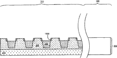
Fig. 2 A and Fig. 2 B show the profile of the memory cell (memory cell 110 that comprises representative) that is arranged in the part in the array 100, and Fig. 2 A is to be along character line 130 along bit line 120 and Fig. 2 B.
Array 100 is included in a memory block 280 and a surrounding zone (the periphery region) 285 on the monocrystalline semiconductor substrate 200.Surrounding zone 285 comprises logic device 286, its have on the gate dielectric 293 with substrate 200 on a grid structure 287, and as the doped region 288,289 of source area and drain region.Grid structure 287 is included in the conductive cap 291 on the DOPOS doped polycrystalline silicon part 290, and is positioned at the dielectric spacer (dielectric spacer) 292 on the sidewall of conductive cap 291 and DOPOS doped polycrystalline silicon part 290.Conductive cap 291 comprises a kind of for example silicide of Ti, W, Co, Ni or Ta that comprises.A kind of conductive plunger 295 is connected to doped region 288 and extends to the end face of dielectric medium 294, and with contact bit line 120b, said dielectric medium 294 comprises one or more layers dielectric material.296 of a kind of conductive plungers are connected to doped region 289 and extend to the end face of dielectric medium 294, with contact wire 297.
Memory block 280 comprises and is arranged in the trap 202 that substrate 200 has one first conductive state (conductivity type), and this trap 202 comprises the second more highly doped doped region 210 of one first doped region 205 and ratio first doped region 205.Substrate 200 comprises that also the position is in trap 202 and extend the character line 130 of first direction; The first direction here is to get into and pass the section shown in Fig. 2 A; And by dielectric irrigation canals and ditches (channel isolating structure) 230 compartments, wherein dielectric irrigation canals and ditches 230 comprise dielectric material to character line 130 in trap.Character line 130 has one second conductive state with respect to first conductive state.
Memory cell 110 comprises a DOPOS doped polycrystalline silicon post (doped polysilicon pillar) 220, DOPOS doped polycrystalline silicon post 220 contact corresponding characters line 130b.DOPOS doped polycrystalline silicon post 220 is higher than the doping of the character line 130b part below the DOPOS doped polycrystalline silicon post 220.Therefore, post 220 and character line 130b connect face defining a pn near 222 places, interface, and said interface 222 most is inner at character line 130b.
Memory cell 110 is included in a conductive cap 240 of DOPOS doped polycrystalline silicon post 220.In illustrated example, conductive cap 240 comprises a kind of for example silicide of Ti, W, Co, Ni or Ta that comprises.Conductive cap 240 provides a low resistance contact (resistance contact) between DOPOS doped polycrystalline silicon post 220 and memory element 125; With by provide one than the polycrystalline silicon material of post 220 more the contact-making surface of high conductivity help to keep the electric current consistent (uniformity) in the DOPOS doped polycrystalline silicon post 220 of operating period, and conductive cap 240 can be during the material chosen property etching post 220 above as protection etch stop (the protective etch stop layer) use of DOPOS doped polycrystalline silicon post 220.In certain embodiments, can omit conductive cap 240.
DOPOS doped polycrystalline silicon post 220 extends through dielectric medium 270 with conductive cap 240.In illustrated example, dielectric medium 270 comprise boron-phosphorosilicate glass (boro-phospho-silicate glass, BPSG) or phosphorosilicate glass (PSG).
Shown in Fig. 2 B; Character line 130 comprises the zone between the DOPOS doped polycrystalline silicon post 220; Its doping than the zone under sept 260 and the DOPOS doped polycrystalline silicon post 220 is high, and this higher doped helps improve the conductance (electrical conductivity) of character line 130 and therefore reduces the load (loading) of character line 130 and improve the consistency (uniformity) of array.In addition, the lighter doped region of the character line 130 under the DOPOS doped polycrystalline silicon post 220 can increase the breakdown voltage (breakdown voltage) that therebetween pn connects face.
DOPOS doped polycrystalline silicon post 220 and the emitter-base bandgap grading of conductive cap 240 as the bipolar junction transistor 115 of memory cell 110.The character line 130b of the part under post 220 is as the base stage of the bipolar junction transistor 115 of memory cell 110.The trap of the part under character line 130b is as the collection utmost point of the bipolar junction transistor 115 of memory cell 110.
Conduction contact hole 215 connects second doped region 210 and electric conducting material 140 of trap 202, and said electric conducting material 140 is linked a reference voltage.
In illustrated example; DOPOS doped polycrystalline silicon post 220 comprises that highly doped N type (N++) polysilicon, character line 130 comprise that the zone of doping P-type material in the substrate 200, zone, second doped region 210 that first doped region 205 comprises doped N-type material in the substrate 200 comprise the zone of highly doped N type (N+) material in the substrate 200, thereby form npn bipolar transistor 115.
In an alternative embodiment; DOPOS doped polycrystalline silicon post 220 comprises that highly doped P type (P++) polysilicon, character line 130 comprise that the zone of doped N-type material in the substrate 200, zone, second doped region 210 that first doped region 205 comprises doping P-type material in the substrate 200 comprise the zone of highly doped P type (P+) material in the substrate 200, thereby form pnp bipolar transistor 115.
Memory element 125 is to be arranged in an opening by an insulation component 245 definition, and electrically connects conductive cap 240 and bit line 120b.The result is that memory element 125 has the bottom surface that has a surface area, and this surface area is less than the surface area of the end face of emitter-base bandgap grading.Memory element 125 for example can comprise one or more materials in the group that is selected from Ge, Sb, Te, Se, In, Ti, Ga, Bi, Sn, Cu, Pd, Pb, Ag, S, Si, O, P, As, N and Au.
Insulation component 245 is preferably the material of the diffusion (diffusion) that comprises the storage medium that can stop memory element 125.In certain embodiments, for hereinafter reason discussed in detail, the material of insulation component 245 can be selected the material of low thermal conductivity (thermal conductivity).
Bit line 120 (comprising the bit line 120b as the top electrode of memory cell 110) extends into and passes the section shown in Fig. 2 B.In illustrated example, bit line 120 comprises one first conductive layer that contacts memory cell and is positioned at one second conductive layer on first conductive layer.Bit line 120 also can select to comprise a single conductive layer.
Bit line 120 has double-deck advantage and comprises for compatible and select the material of first conductive layer with the material of memory element 125, simultaneously for other advantage like the conductance higher than the material of first conductive layer, and select the material of second conductive layer.In illustrated example, first conductive layer comprises that the TiN and second conductive layer comprise Al.Comprise that at memory element 125 TiN is suitable for as first conductive layer among the embodiment of GST (will in the hereinafter discussion); Because it can have excellent contact with GST; TiN is a kind of general material that is used for the semiconductor manufacturing, and it provides a good diffusion barrier (diffusionbarrier).It is TaN, TiAlN or TaAlN that first conductive layer also can be selected.
As other example, first and second conductive layer of bit line 120 can comprise separately and is selected from the group that comprises Ti, W, Mo, Al, Ta, Cu, Pt, Ir, La, Ni, N, O and Ru and one or more elements in its combination.
In illustrated example, electric conducting material 140 and lead 297 also comprise first and second conductive layer of first and second conductive layer such as corresponding lines 120.In addition, electric conducting material 140 and lead 297 can comprise one or more layers material separately, and it for example comprises above-mentioned one or more elements that relevant bit line 120 is discussed separately.
Insulation component 245 has side (sides) 246, and it is in vertical alignment with the side 221 of emitter-base bandgap grading (DOPOS doped polycrystalline silicon post 220 and conductive cap 240), so that define sidewall 262.Also have 260 of sidewall spacers that comprises dielectric material on sidewall 262 and around emitter-base bandgap grading and insulation component 245.
When projection was on emitter-base bandgap grading, the side 221 of emitter-base bandgap grading defined a cylinder (cylinder) above emitter-base bandgap grading.In the illustrated example of Fig. 2 A~Fig. 2 B, by the cylinder of side 221 definition side 246 as insulation component 245.In illustrated example, because the circular section of emitter-base bandgap grading, has a circular section so have cylinder by side 221 definition of emitter-base bandgap grading.By the cylinder of the side of emitter-base bandgap grading 221 definition section shape, also can select to have square (square), oval, rectangle or erose a little section according to emitter-base bandgap grading.
In the profile shown in Fig. 2 A~Fig. 2 B; Insulation component 245 has an opening; Be placed on by the center in the cylinder of the side of emitter-base bandgap grading 221 definition, and memory element 125 is to place opening and be self-aligned to emitter-base bandgap grading (DOPOS doped polycrystalline silicon post 220 and conductive cap 240).Relevant below Fig. 4~Figure 17 institute is more among the manufacturing embodiment of detailed description; DOPOS doped polycrystalline silicon post 220 is during the patterning of material, to form with conductive cap 240, and said patterning is in order to the insulation component 245 that the defines follow-up formation position with memory element 125.Then, form sept 260 material that is patterned of selective removal again, to form one by sept 260 definition and the interlayer hole of position on conductive cap 240.Then, in interlayer hole, form insulation component 245 and have an opening that is placed on the center of conductive cap 240, in by insulation component 245 defined openings, form memory element 125 again.
Moreover during relevant below Fig. 4~Figure 17 institute describes in detail more, in memory block and surrounding zone, form grid dielectric material.Remove said grid dielectric material from the memory block, in memory block and surrounding zone, form one deck doped polycrystalline silicon materials and one deck conductive cap material then.Utilize the material of this layer doped polycrystalline silicon materials to form the grid of logic device and the emitter-base bandgap grading of bipolar junction transistor access device afterwards with this layer conductive cap material.As a result, comprise in the storage device of this description and having and bipolar junction transistor access device that the CMOS peripheral circuit is compatible and satisfy design and integrate the phase-change memory cell with technology.
In operation, voltage on bit line 120b and character line 130b can respond to an electric current and flow to the collection utmost point via memory cell 110 from emitter-base bandgap grading.
Active region 128 is zones of memory element 125, and the storing therein material is lured into and between at least two kinds of solid phases, changed.Should know that said active region 128 can be done minimumly in the structure of explanation, reduce the amount of luring the electric current that phase change is required into thus.By the width 129 of the memory element 125 in the insulation component 245 defined openings less than the width of DOPOS doped polycrystalline silicon post 220 with conductive cap 240, and be preferably less than being used for forming DOPOS doped polycrystalline silicon post 220, conductive cap 240 minimum feature size (feature size) with the technology (like photoetching process) of bit line 120.Little width 129 has been concentrated the current density in the memory element 125, reduces the amount of the required electric current of the phase change of luring in the active region 128 thus.In addition, insulation component 245 can provide some thermal isolations of active region 128, and this also can help to reduce the magnitude of current of luring that phase change is required into.Moreover the remainder of memory element 125 can provide active region 128 some thermal isolations from bit line 120b.
As stated, bipolar junction transistor can provide the current drives bigger than field-effect transistor.In addition, because transistorized emitter-base bandgap grading comprises the doped polycrystalline silicon materials, thus can obtain a sizable current gain (gain), thus be reduced in the required magnitude of current of phase change of luring on the bit line 120b in the memory element.The magnitude of current in the reduction on the character line 130 has reduced the cross-talk (cross-talk) between the device of sharing same character line, and then improves the effect of array.The electric current of the reduction on character line 130 also can be avoided parasitic BJT behavior (parasitic BJT behavior), that is the emitter-base bandgap grading in the memory cell of a vicinity becomes a collection utmost point.
Fig. 3 A show similar Fig. 2 A~Fig. 2 B embodiment the profile of second embodiment, a top conductor (top conductor) 300 is wherein arranged, it comprises the silicide on the end face of this higher doped of character line 130.Top conductor 300 comprises a kind of for example silicide of Ti, W, Co, Ni or Ta that comprises.Top conductor 300 has increased the conductance (electrical conductivity) of character line 130 and has therefore reduced the firing current (turn on current) and the load of character line 130, thereby causes the consistency (uniformity) of array.The top conductor 300 that comprises silicide also can be removed minority carrier from character line 130 to avoid parasitic BJT behavior.Simultaneously, shown in figure 21, in certain embodiments, on the sidewall of character line 130, form the sidewall conductor 1900 that comprises silicide.Sidewall conductor 1900 can be removed from the minority carrier of character line and the conductance of promoting character line 130.
Embodiment in the memory cell of this description comprises the phase-change storage material that is used for memory element, comprises chalcogenide material or other material.Chalcogen (chalcogens) comprises any in these four elemental oxygens (O), sulphur (S), selenium (Se) and the tellurium (Te), and it forms the part of V IA family of periodic table.Chalcogenide comprises a kind of chalcogen and a kind of than the element of electropositive or the compound of root (radical).Chalcogenide alloy comprises chalcogenide and other constituent like other material of transition metal.A kind of chalcogenide alloy comprises one or more element usually, and it is from the IVA family of the periodic table of elements, like germanium (Ge) and tin (Sn).Chalcogenide alloy always comprises antimony (Sb), gallium (Ga), indium (In), silver (Ag) one of them or multiple constituent.A lot of phase-change storage materials have been described in the technical literature, comprising: the alloy of Ga/Sb, In/Sb, In/Se, Sb/Te, Ge/Te, Ge/Sb/Te, In/Sb/Te, Ga/Se/Te, Sn/Sb/Te, In/Sb/Ge, Ag/In/Sb/Te, Ge/Sn/Sb/Te, Ge/Sb/Se/Te and Te/Ge/Sb/S.In the family of Ge/Sb/Te alloy, perhaps the alloy mixture (compositions) of wide scope is feasible.Said mixture can TeaGebSb100-(a+b) as characteristic.Existing researcher describes the most useful alloy, and its mean concentration that in deposition materials, has Te is below 70%, the typical case be 60% below and generally be low to about 23% and the scope of high about 58%Te of arriving, optimum ground is about 48%~58%.The concentration of Ge about more than 5% and in material on average from about 8% the low spot scope to about 30%, remaining is usually less than 50%.Optimal is that the concentration of Ge is in about 8% to about 40% scope.And the clout of the main component in this mixture is Sb.These percentages are atomic percents (atomic percentages) of whole 100% of the atom of component.(the 10th~11 hurdle of the United States Patent (USP) 5687112 of Ovshinsky).The particular alloy that is proposed by other researcher comprises Ge 2Sb 2Te 5, GeSb 2Te 4With GeSb 4Te 7(Noboru Yamada " Potential of Ge-Sb-Te Phase-Change Optical Disks for High-Data-RateRecording ", SPIE v.3109, pp.28-37 (1997)).More general combines with its mixture or alloy a kind of transition metal like chromium (Cr), iron (Fe), nickel (Ni), niobium (Nb), palladium (Pd), platinum (Pt) with Ge/Sb/Te, have a kind of phase-change alloy of programming resistors characteristic with formation.The object lesson of the useful storage medium that in the 11st~13 hurdle of Ovshinsky ' 112, is proposed will merge as reference to be used.
In certain embodiments, but impurity (impurities) is in chalcogenide and other phase-change material, so that the chalcogenide that use to mix changes other characteristic of conductance, transition temperature, fusion temperature and memory element.The impurity of representative of chalcogenide of being used for mixing comprises nitrogen, silicon, oxygen, silicon dioxide, silicon nitride, copper, silver, gold, aluminium, aluminium oxide, tantalum, tantalum oxide, tantalum nitride, titanium and titanium oxide.For example ask for an interview u. s. patent numbers 6800504 and U.S. Patent Publication 2005/0029502.
Can the switch phase-change alloy between one first structure attitude and one second structure attitude, the first structure attitude is that material is that amorphous solid phase, the second structure attitude are that material is crystalline solid phase usually therein usually therein in its local order (local order) in the active channel district of unit.These alloys are bistable state at least.So-called amorphous is represented a kind of ordered structure more unordered, more less relatively than monocrystalline (orderedstructure), and it has can detect characteristic like the resistivity higher than crystalline phase (resistivity).So-called crystallization is a kind of structure orderly, comparatively more orderly than non crystalline structure of expression, and it has can detect characteristic like the resistivity lower than amorphous phase.General phase-change material can be by switch between the different bistable states of electric power in the local order of passing the scope (spectrum) between complete amorphous state and the complete crystalline state.All the other receive amorphous phase to comprise atomic number degree (atomic order), free electron density and activation energy with the material characteristics that influences mutually between the crystalline phase.It is exactly the mixture (mixture) that converts two or more solid phases to that such material does not convert different solid phases to, to be provided at the GTG (gray scale) between complete amorphous state and the complete crystalline state.Therefore the electrical characteristics in this kind material are changeable.
Phase-change alloy can be converted to another from a phase by the utilization of electric pulse.Known a kind of weak point, higher width of cloth pulse (amplitude pulse) help to make phase-change material to be transformed into general amorphous state.And a kind of length, lower width of cloth pulse help to make phase-change material to be transformed into general crystalline state.Energy in short, higher width of cloth pulse is high to the key that can interrupt crystalline texture and short as to avoid atom to be combined into crystalline state again.Be fit to the proper data curve of the pulse of specific phase-change alloy, but do not need just concrete decision of undo experimentation.In the chapters and sections below, phase-change material is to be example with GST, and should know the phase-change material that also can use other kind.Describing for accomplishing the useful material of a kind of PCRAM at this is Ge 2Sb 2Te 5
Can use other programmable resistance storage medium in other embodiments of the invention, comprise other material that uses different crystalline phases to decide resistance, or use electric pulse to change other storage medium of resistance value state (resistance state).These examples comprise and are used for resistive random access memory ((metal-oxides) comprises tungsten oxide (WO like metal oxide for resistance random access memory, material RRAM) X), NiO, Nb 2O 5, CuO 2, Ta 2O 5, Al 2O 3, CoO, Fe 2O 3, HfO 2, TiO 2, SrTiO 3, SrZrO 3Or (BaSr) TiO 3Additional example comprises that being used to similarly is that turning moment shifts (spin-torque-transfer; STT) magnetoresistive random access memory (magnetoresistance random access memory; MRAM) material of MRAM, for example CoFeB, Fe, Co, Ni, Gd, Dy, CoFe, NiFe, MnAs, MnBi, MnSb, CrO 2, MnOFe 2O 3, FeOFe 2O 5, NiOFe 2O 3, MgOFe 2, EuO and Y 3Fe 5O 12At least wherein a kind of.Ask for an interview the U.S. Patent Publication 2007/0176251 for " Magnetic Memory device and Methodof Fabricating the Same " of exercise question for example, it merges as with reference to using at this.Additional example also comprises and is used for programmable metallization unit (programmable-metallization-cell; PMC) memory or how solid electrolyte (solid electrolyte) material of rice ion stores (nano-ionic memory) are such as the germanium sulfide electrolyte of silver-doped and the germanium sulfide electrolyte of copper doped.Ask for an interview " A macro model of programmable metallization cell devices, " Solid-StateElectronics 49 (2005) 1813~1819 that N.E.Gilbert et al. is for example shown, it merges as with reference to using at this.
A kind of exemplary method that forms chalcogenide is under the pressure of 1mTorr~100mTorr, to utilize PVD sputter or magnetic control sputtering plating method and Ar, N 2, and/or the source gas of He etc.Such deposition is normally carried out in room temperature.Use a kind of depth-width ratio to improve stowage capacity (fill-in performance) at 1~5 collimator (collimator).Also can improve stowage capacity with tens of volts to hundreds of volts DC bias voltage.On the other hand, can use combining of DC bias voltage and collimator simultaneously.For disclosing a kind of exemplary method of utilizing chemical vapor deposition (CVD) to form chalcogenide in the U.S. Patent Publication 2006/0172067 of " Chemical Vapor Deposition of Chalcogenide Materials ", it is merged as reference at this uses in exercise question.In Lee; Et al. " HighlyScalable Phase Change Memory with CVD GeSbTe for Sub 50nmGeneration ", the pp.102-103 on the symposium (Symposium) of VLSI Technology Digest of Technical Papers in 2007 has disclosed other exemplary method of utilizing CVD to form chalcogenide.
Optionally implement a kind of under vacuum or N 2Deposition after annealing under the environment is handled (post-deposition annealing treatment), to improve the crystalline state of chalcogenide material.And above-mentioned annealing temperature is lower than 30 minutes at 100 ℃ to 400 ℃ scope and annealing time usually.
Fig. 4~Figure 17 B shows a kind of step of production order of array of the memory cell of making the bipolar junction transistor with band polysilicon emitter-base bandgap grading and autoregistration memory element described here.
Fig. 4 shows the first step that forms a substrate, this substrate comprise the position the memory block 280 that contains first and second doped region 205,210 in trap 202 and in trap 202 and extend into and pass the dielectric irrigation canals and ditches 230 of section shown in Figure 4.First and second doped region 205,210 can use known implantation and activation annealing technology to form.In illustrated example, first doped region 205 comprises the substrate 200 of doped N-type material, the substrate 200 that second doped region 210 comprises highly doped N type (N+) material.In the embodiment that substitutes, first doped region 205 comprises the substrate 200 of doping P-type material, the substrate 200 that second doped region 210 comprises highly doped P type (P+) material.
Then, in first doped region 205 of trap, form character line 130 by implantation step, the result obtains the structure shown in the profile of Fig. 5 A and Fig. 5 B.In illustrated example, in trap, form a high-doped zone simultaneously, extend to second doped region 210 from substrate 200 end faces by one second ion implantation step.Character line 130 has second conductive state, and in illustrated example, character line 130 comprises the substrate 200 of doping P-type material.In the embodiment that substitutes, character line 130 comprises the substrate 200 of doped N-type material.
Then, form gate dielectric 293 on Fig. 5 A in memory block 280 and surrounding zone 285 and the structure shown in Fig. 5 B, the result obtains structure shown in Figure 6.In illustrated example, gate dielectric 293 comprises silicon dioxide.
Afterwards; Remove the gate dielectric 293 in the memory block 280 of structure shown in Figure 6; Form the doped polycrystalline silicon materials that one deck 700 has first conductive state again, on doped polysilicon layer 700, form one deck 710 conductive cap materials then, the result obtains the structure shown in the profile of Fig. 7 A and Fig. 7 B.Conductive cap material layer 710 comprises a kind of silicide that for example contains Ti, W, Co, Ni or Ta.In one embodiment, this layer 710 comprises cobalt silicide (cobalt silicide is CoSi) and by deposition one deck cobalt and carry out a rapid hot technics (RTP) and forms, so that the pasc reaction in cobalt and the layer 700 and form said layer 710.Should know the also available mode that is similar to the example of use cobalt described herein of other silicide, form by the mode of the deposition of the nickel of titanium, arsenic, doping or its alloy.
Then, in the surrounding zone 285 of the structure shown in Fig. 7 A and Fig. 7 B, form logic device 286, the result obtains the structure shown in Fig. 8 A and Fig. 8 B.In illustrated example; The formation of logic device 286 comprises; Form the DOPOS doped polycrystalline silicon part 290 and conductive cap 291 of grid structure 287 by the said layer 700 and 710 in the patterning surrounding zone 285; Implement a shallow doped-drain (LDD) again and implant technology; After in the substrate 200 of adjacent gate structures 287, forming shallow doped region, on the sidewall of conductive cap 291 and DOPOS doped polycrystalline silicon part 290, form an insulating barrier 292, implement one second again and implant technology, to form as the source electrode of logic device 286 and the doped region 288 and 289 of drain electrode.Certainly also can use other technology to form logic device 286.
Then, on the structure shown in Fig. 8 A and Fig. 8 B, form one deck 900 dielectric materials, the result obtains the structure shown in Fig. 9 A and Fig. 9 B.In illustrated example, said layer 900 comprises silicon nitride.
Then, the said layer 900,700 and 710 in the memory block 280 of patterning Fig. 9 A and Fig. 9 B, on character line 130, to form a plurality of multilayer laminated (multi-layer stacks) 1000, the result obtains the structure shown in Figure 10 A and Figure 10 B.For example be by on multilayer laminated 1000 locational said layer 900, forming a mask (a for example patterned photoresist), re-use said mask and come the said layer 900,700 and 710 of eating thrown, forming multilayer laminated 1000 as etching mask.
Can know from Figure 10 A and Figure 10 B; Multilayer laminated 1000 comprise DOPOS doped polycrystalline silicon post 220, its be included on the corresponding word line acts 130 near define between the interface 222 pn connect the material of the said layer 700 (asking for an interview Fig. 9 A and Fig. 9 B) of face, in a conductive cap 240 of the material that comprises said layer 700 (asking for an interview Fig. 9 A and Fig. 9 B) on the post 220, reach the sacrificial member (sacrificial element) 1010 of the material that on conductive cap 240, comprises said layer 900.
In illustrated example, multilayer laminated 1000 have a circular section.In other embodiments, can be according to the manufacturing technology that is used to form multilayer laminated 1000, make multilayer laminated 1000 to have square, oval, rectangle or difform a little section.
Then; On multilayer laminated 1000 sidewall, form the sidewall spacer 260 that comprises dielectric material; Carry out one again and implant the higher doped (more highly doped regions) that technology forms the character line 130 between adjacent wall sept 260; On the higher doped of character line 130, form the top conductor (top conductors) 300 that comprises self-aligned silicide (salicide) then, the result obtains the structure shown in Figure 11 A and Figure 11 B.In certain embodiments, can omit above-mentioned top conductor 300.
The formation of sidewall spacer 260 can be owing to the conforma layer (conformal layer) of deposition one deck sidewall spacer material on the structure shown in Figure 10 A and Figure 10 B, and non-again grade is to the said conforma layer of ground etching, to form above-mentioned sidewall spacer 260.During the silicide process that forms top conductor 300, the interface that sidewall spacer 260 meeting protection laminations 1000 and lamination 1000 and character line are 130.
In one embodiment, top conductor 300 comprises that the formation of cobalt silicide (CoSi) and top conductor 300 is by deposition one deck cobalt and carries out a rapid hot technics (RTP) so that the pasc reaction in cobalt and the character line 130 and form said top conductor.Should know the also available mode that is similar to the example of use cobalt described herein of other silicide, form by the mode of the deposition of the nickel of titanium, arsenic, doping or its alloy.
Subsequently; On the structure shown in Figure 11 A~Figure 11 B, form one dielectric layer 270; Carry out a flatening process (planarization process) like CMP again to expose the end face of multilayer laminated 1000 sacrificial member 1010, the result obtains the structure shown in Figure 12 A and Figure 12 B.
Then, form conduction contact hole 215 arrays that pass dielectric layer 270, with second doped region 210 that contacts said trap and the conductive plunger 295,296 that forms difference contact doping district 288 and 289, the result obtains the structure shown in Figure 13 A and Figure 13 B.
Then, remove the sacrificial member 1010 of Figure 13 A and Figure 13 B, to form the interlayer hole 1400 that is defined by sept 260, it down extends to conductive cap 240, and the result obtains the structure shown in Figure 14 A and Figure 14 B.
Afterwards, in the interlayer hole 1400 of Figure 14 A and Figure 14 B, form insulation component 245, the result obtains the structure shown in Figure 15 A and Figure 15 B.Insulation component 245 defines the opening (self-centered opening) 1510 that comes from centring in interlayer hole 1400, and in illustrated example, insulation component 245 comprises silicon nitride.
The formation of insulation component 245 can be by forming one deck insulative dielectric material layer on the structure shown in Figure 14 A and Figure 14 B, non-again grade is to the said dielectric materials layer of ground etching, to expose the conductive cap 240 of a part.
The formation of said insulation component 245 also can be selected forming one deck has opening on interlayer hole 1400 material layer on the end face of dielectric layer 270 earlier.The material layer on the end face of dielectric layer 270 then, on interlayer hole 1400, carries out one selectivity and crosses and cut (undercutting) etching, so that can intactly be stayed.Then, in interlayer hole 1400, form insulating layer material, and since selectivity cross and cut etch process and cause being formed on an autoregistration hole (void) is arranged in the insulating layer material in the interlayer hole 1400.Then; On insulating layer material, carry out an anisotropic etch process; To open described hole, a part of end face that continues the conductive cap 240 in the zone of etching under hole again comes out, and in interlayer hole 1400, forms the insulation component 245 that comprises insulating layer material thus.
Then, in the insulation component 245 defined openings 1510 by the structure shown in Figure 15 A~Figure 15 B, form memory element 125, the result obtains the structure shown in Figure 16 A~Figure 16 B.The formation of memory element 125 can be followed the flatening process like CMP one again by on the structure shown in Figure 15 A~Figure 15 B, depositing storage medium earlier.
Then, on the structure shown in Figure 16 A~Figure 16 B, form bit line 120, link the electric conducting material 140 and the lead 297 of a reference voltage (reference voltage), the result obtains the structure shown in Figure 17 A~Figure 17 B.In illustrated example, bit line 120 electric conducting materials 140 and lead 297 comprise first and second conductive layer, and by deposition said first and second conductive layer again patterning and form.
As stated, DOPOS doped polycrystalline silicon post 220 and conductive cap 240 are during the sacrificial member 1010 of the insulation component 245 of the follow-up formation of definition and the position of memory element 125 forms, to form.Then, form sept 260, the selective removal sacrificial member 1010 again, are positioned on the conductive cap 240 and by sept 260 defined interlayer holes 1400 with formation.Then in interlayer hole 1400, form insulation component 245, it has the opening that places by the center in the defined cylinder in the side of emitter-base bandgap grading, in by insulation component 245 defined openings 1510, forms memory element 125 afterwards.Therefore, the memory element position in DOPOS doped polycrystalline silicon post 220 and conductive cap 240 in the heart and be self-aligned to DOPOS doped polycrystalline silicon post 220 and conductive cap 240, and DOPOS doped polycrystalline silicon post 220 and the emitter-base bandgap grading of conductive cap 240 as the bipolar junction transistor of memory cell.
Because make simultaneously have bipolar junction transistor in logic device and the memory block in the surrounding zone memory cell in above-mentioned manufacturing step; So compatibility (compatibility) problem that storage device has the complexity (complexity) of reduction and satisfies the design integration of above-mentioned discussion is to reduce cost.As stated, bipolar junction transistor can provide the current drives bigger than field-effect transistor.In addition because transistorized emitter-base bandgap grading comprises the doped polycrystalline silicon materials, so can obtain sizable current gain, thereby reduce the phase change cause in the memory element and on character line 130 the required magnitude of current.The magnitude of current in reduction on the character line 130 will reduce the cross-talk (cross-talk) between the device of sharing the identical characters line, and then improves the effect of array.
Figure 18~Figure 21 shows a kind of alternate embodiment to the formation character line 130 that in Fig. 5 A~Fig. 5 B, shows.
Shown in the profile of Figure 18, carry out the dielectric material of a part that etching removes the dielectric irrigation canals and ditches 230 of Fig. 4, with the side wall surface 1800 of first doped region 205 of the trap that exposes 230 in dielectric irrigation canals and ditches.
Then, on the side wall surface that exposes 1800 of first doped region 205 of the trap of Figure 18, form sidewall conductor 1900, the result obtains the structure shown in the profile of Figure 19.Said sidewall conductor 1900 comprises a kind of silicide that for example contains Ti, W, Co, Ni or Ta.The formation of sidewall conductor 1900 can be annealed by on the side wall surface that exposes 1800, depositing a silicide predecessor (precursor) earlier again, so that silicide forms.Remove remaining silicide predecessor in the substrate then, stay the self-aligned silicide sidewall conductor on the side of side wall surface 1800.Typical silicide predecessor comprises compound such as cobalt, titanium, nickel, molybdenum, tungsten, tantalum and the platinum of metal or metal.Simultaneously, said silicide predecessor also can comprise metal nitride or other metal mixture.Final silicide sidewall conductor 1900 can be from character line removal minority carrier and the conductance of promoting character line 130.
Then, on structure shown in Figure 19, form dielectric material inserting dielectric irrigation canals and ditches 230, the result obtains the structure shown in the profile of Figure 20.
Subsequently, carry out ion and implant to implant admixture (dopants) and form character line 130, this character line 130 has and first and second doped regions 205 of trap and 210 the opposite conductive state of conductive state, and the result obtains the structure shown in the profile of Figure 21.
Figure 22 is a kind of calcspar of simplification of integrated circuit 2210, and aforementioned integrated circuit 2210 comprises an a kind of memory cell array 100 of borrowing the memory cell realization of using the bipolar junction transistor with band polysilicon emitter-base bandgap grading and autoregistration memory element described here.Have a wordline decoders 2214 that reads, sets with replacement pattern (read, set, and reset modes) and be connected to and be connected in electrically a plurality of a plurality of character lines 2216 of in storage array 100, arranging along row (rows).(OK) decoder 2218 is connected in storage array 100 along a plurality of positions 22220 that row (columns) is arranged electrically, in order to read, set and the array 100 of resetting in phase-change memory cell (not illustrating).Supply address (addresses) is to wordline decoders and driver 2214 and bit line decoder 2218 on bus (bus) 2222.In square 2224, comprise and be used to read, set and the voltage source of the pattern of resetting and/or the sensing amplifier (sense amplifiers) of current source (current source) are linked bit line decoder 2218 with the Data-In structure via data/address bus 2226.Output/input (input/output) interface (ports) from integrated circuit 2210 provides data to the Data-In structure the square 2224 via a data-in lead 2228, or supplies data to the Data-In structure the square 2224 from the inside or the outside Data Source of other integrated circuit 2210.2230 in other circuit (Other circuitry) can be included in the integrated circuit 2210; Like general processor (general purpose processor) or specific purposes application circuit, or a kind of module combinations (combination) that system single chip (system-on-a-chip) function of being supported by array 100 is provided.Sensing amplifier from square 2224 is provided to the output/input interface on the integrated circuit 2210 via a data-out lead 2232 with data, or data are provided to inside or outside other data endpoint (datadestinations) of integrated circuit 2210.
The controller that provides in the example here (controller) 2234 uses bias arrangement state machines (bias arrangement state machine) to control the utilization of bias arrangement supply voltage and current and power supply 2236, as read, programme, wipe, erase verification (erase verify) and program verification voltage and/or electric current.Can use special purpose (special-purpose) logical circuit in the known technology to accomplish controller 2234.In the embodiment that substitutes, controller 2234 comprises a general processor, and it can be realized on identical integrated circuit, controls the operation of said device to carry out a computer program.In another embodiment, controller 2234 is accomplished in the combination of special purpose (special-purpose) logical circuit also capable of using and general processor.
Though the present invention discloses as above with embodiment; Right its is not in order to limit the present invention; Has common knowledge the knowledgeable in the technical field under any; Do not breaking away from the spirit and scope of the present invention, when can doing a little change and retouching, so protection scope of the present invention is when looking being as the criterion that the claim scope defined.

Claims (27)

1.一种包括多个存储单元的储存装置,在该多个存储单元中的一个存储单元包括:1. A storage device comprising a plurality of storage units, one storage unit in the plurality of storage units comprising: 一双极接面晶体管,包括一射极,该射极包括一掺杂多晶硅柱,该掺杂多晶硅柱接触对应的字符线,该掺杂多晶硅柱比该掺杂多晶硅柱下面的字符线部分的掺杂要更高,该掺杂多晶硅柱与字符线在接近界面处定义出一个pn接面;A bipolar junction transistor, including an emitter, the emitter includes a doped polysilicon column, the doped polysilicon column contacts the corresponding word line, the doped polysilicon column is more doped than the word line portion below the doped polysilicon column The impurity is higher, and the doped polysilicon column and the word line define a pn junction near the interface; 一绝缘元件,位在该射极上并具有延伸穿过该绝缘元件的一开口,该开口位在该射极上的中心;以及an insulating element on the emitter and having an opening extending through the insulating element, the opening being centered on the emitter; and 一存储元件,位在该开口内并与该射极电性相连。A storage element is located in the opening and electrically connected with the emitter. 2.如权利要求1所述的包括多个存储单元的储存装置,其中:2. The storage device comprising a plurality of storage units according to claim 1, wherein: 当该多个存储单元的该掺杂多晶硅柱投影于该射极上,在该射极上定义出一柱面的侧边;以及When the doped polysilicon columns of the plurality of memory cells are projected onto the emitter, defining a side of a column on the emitter; and 该开口位在该柱面内的中心。The opening is located at the center of the cylinder. 3.如权利要求1所述的包括多个存储单元的储存装置,其中该多个存储单元的该多个存储元件具有一表面积的底面,该表面积小于对应的该射极的顶面的表面积。3. The memory device comprising a plurality of memory cells as claimed in claim 1, wherein the plurality of memory elements of the plurality of memory cells have a bottom surface with a surface area smaller than a surface area of a corresponding top surface of the emitter. 4.如权利要求1所述的包括多个存储单元的储存装置,其中该多个存储单元的该射极还包括一导电盖,位在该掺杂多晶硅柱上,该导电盖包括一硅化物。4. The storage device comprising a plurality of memory cells as claimed in claim 1, wherein the emitters of the plurality of memory cells further comprise a conductive cap on the doped polysilicon pillar, the conductive cap comprising a silicide . 5.如权利要求1所述的包括多个存储单元的储存装置,其中该多个存储单元的该绝缘元件具有一外表面垂直对准于对应的该射极的一外表面。5. The storage device comprising a plurality of memory cells as claimed in claim 1, wherein the insulating element of the plurality of memory cells has an outer surface vertically aligned with an outer surface of the corresponding emitter. 6.如权利要求5所述的包括多个存储单元的储存装置,其中在该多个存储单元中的存储单元还包括一侧壁间隔物环绕该绝缘元件与该射极。6. The storage device comprising a plurality of memory cells as claimed in claim 5, wherein the memory cells in the plurality of memory cells further comprise a sidewall spacer surrounding the insulating element and the emitter. 7.如权利要求1所述的包括多个存储单元的储存装置,还包括一单晶基底以及位在该单晶基底中的多个字符线,该多个存储单元的该射极接触该多个字符线中的一对应字符线,其中该多个存储单元的该双极接面晶体管还包括:7. The storage device comprising a plurality of memory cells as claimed in claim 1, further comprising a single crystal substrate and a plurality of word lines positioned in the single crystal substrate, the emitters of the plurality of memory cells contact the multiple A corresponding word line in the word lines, wherein the bipolar junction transistors of the plurality of memory cells also include: 位于该射极下的一部分的该对应字符线,以作为一基极;以及a portion of the corresponding word line under the emitter as a base; and 一集极,包括位于该基极下的一部分的该单晶基底。A collector includes a portion of the single crystal substrate underlying the base. 8.如权利要求7所述的包括多个存储单元的储存装置,其中该多个字符线还包括位在相连的该多个存储单元的该射极之间的区域的顶表面上的多个顶导体,该多个顶导体包括硅化物。8. The storage device comprising a plurality of memory cells as claimed in claim 7, wherein the plurality of word lines further comprise a plurality of top conductors, the plurality of top conductors comprising suicide. 9.如权利要求7所述的包括多个存储单元的储存装置,还包括位在该多个字符线的侧壁表面上的多个侧壁导体,该多个侧壁导体包括硅化物。9. The memory device comprising a plurality of memory cells of claim 7, further comprising a plurality of sidewall conductors on sidewall surfaces of the plurality of word lines, the plurality of sidewall conductors comprising silicide. 10.如权利要求7所述的包括多个存储单元的储存装置,其中:10. The storage device comprising a plurality of storage units according to claim 7, wherein: 该单晶基底包括n型掺杂半导体材料;The single crystal substrate includes n-type doped semiconductor material; 该多个字符线包括p型掺杂半导体材料;以及The plurality of word lines comprise a p-type doped semiconductor material; and 该多个存储单元的该射极包括n型掺杂多晶硅。The emitters of the plurality of memory cells include n-type doped polysilicon. 11.如权利要求7所述的包括多个存储单元的储存装置,其中:11. The storage device comprising a plurality of storage units according to claim 7, wherein: 该单晶基底包括p型掺杂半导体材料;The single crystal substrate includes a p-type doped semiconductor material; 该多个字符线包括n型掺杂半导体材料;以及The plurality of word lines comprise n-type doped semiconductor material; and 该多个存储单元的该射极包括p型掺杂多晶硅。The emitters of the plurality of memory cells include p-type doped polysilicon. 12.如权利要求7所述的包括多个存储单元的储存装置,还包括多个位线,其中该多个存储单元的该多个存储元件电性相连至该射极与该多个位线中的一对应位线之间。12. The storage device comprising a plurality of memory cells according to claim 7, further comprising a plurality of bit lines, wherein the plurality of storage elements of the plurality of memory cells are electrically connected to the emitter and the plurality of bit lines between a pair of corresponding bit lines. 13.如权利要求12所述的包括多个存储单元的储存装置,还包括多个导电接触窗,接触该单晶基底并连到一参考电压。13. The storage device comprising a plurality of memory cells as claimed in claim 12, further comprising a plurality of conductive contacts contacting the single crystal substrate and connected to a reference voltage. 14.一种制造储存装置的方法,包括形成多个存储单元,在形成该多个存储单元的方法中,至少有一个方法包括:14. A method of manufacturing a memory device, comprising forming a plurality of memory cells, at least one of the methods of forming the plurality of memory cells comprising: 形成一双极接面晶体管,该双极接面晶体管包括一射极,该射极包括一掺杂多晶硅柱,该掺杂多晶硅柱接触对应的字符线,该掺杂多晶硅柱比该掺杂多晶硅柱下面的字符线部分的掺杂要更高,该掺杂多晶硅柱与字符线在接近界面处定义出一个pn接面;A bipolar junction transistor is formed, the bipolar junction transistor includes an emitter, the emitter includes a doped polysilicon column, the doped polysilicon column contacts the corresponding word line, and the doped polysilicon column is larger than the doped polysilicon column The doping of the lower part of the word line is higher, and the doped polysilicon column and the word line define a pn junction near the interface; 在该射极上形成一绝缘元件,该绝缘元件具有延伸穿过该绝缘元件的一开口,该开口位在该射极上的中心;以及forming an insulating element on the emitter, the insulating element having an opening extending through the insulating element, the opening being centrally located on the emitter; and 在该开口内形成一存储元件,且该存储元件与该射极电性相连。A storage element is formed in the opening, and the storage element is electrically connected to the emitter. 15.如权利要求14所述的制造储存装置的方法,其中:15. The method of manufacturing a storage device according to claim 14, wherein: 当该多个存储单元的该掺杂多晶硅柱投影于该射极上,在该射极上定义出一柱面的侧边;以及When the doped polysilicon columns of the plurality of memory cells are projected onto the emitter, defining a side of a column on the emitter; and 该开口位在该柱面内的中心。The opening is located at the center of the cylinder. 16.如权利要求14所述的制造储存装置的方法,其中该多个存储单元的所述射极还包括一导电盖,位在该掺杂多晶硅柱上,该导电盖包括一硅化物。16. The method of manufacturing a storage device as claimed in claim 14, wherein the emitters of the plurality of memory cells further comprise a conductive cap on the doped polysilicon pillar, the conductive cap comprising a silicide. 17.如权利要求14所述的制造储存装置的方法,其中该多个存储单元的该绝缘元件具有一外表面垂直对准于对应的该射极的一外表面。17. The method of manufacturing a memory device as claimed in claim 14, wherein the insulating elements of the plurality of memory cells have an outer surface vertically aligned with an outer surface of the corresponding emitter. 18.如权利要求17所述的制造储存装置的方法,其中形成该多个存储单元还包括形成一侧壁间隔物环绕该绝缘元件与该射极。18. The method of manufacturing a memory device as claimed in claim 17, wherein forming the plurality of memory cells further comprises forming a sidewall spacer surrounding the insulating element and the emitter. 19.如权利要求14所述的制造储存装置的方法,还包括:19. The method of manufacturing a storage device as claimed in claim 14, further comprising: 形成一单晶基底;forming a single crystal substrate; 在该单晶基底中形成多个字符线,该多个存储单元的该射极接触该多个字符线中的一对应字符线,其中该多个存储单元的该双极接面晶体管还包括位于该射极下的部分该对应字符线作为一基极,以及包括位于该基极下的一部分的该单晶基底的一集极;以及A plurality of word lines are formed in the single crystal substrate, the emitters of the plurality of memory cells contact a corresponding word line in the plurality of word lines, wherein the bipolar junction transistors of the plurality of memory cells also include a portion of the corresponding word line under the emitter as a base, and a collector including a portion of the single crystal substrate under the base; and 形成多个位线,其中该多个存储单元的该多个存储元件电性相连于该射极与所述位线中的一对应位线之间。A plurality of bit lines are formed, wherein the plurality of storage elements of the plurality of memory cells are electrically connected between the emitter and a corresponding one of the bit lines. 20.如权利要求19所述的制造储存装置的方法,其中形成该多个字符线,还包括在相连的该多个存储单元的该射极之间的区域的顶表面上形成多个顶导体,该多个顶导体包括硅化物。20. The method for manufacturing a storage device as claimed in claim 19, wherein forming the plurality of word lines further comprises forming a plurality of top conductors on the top surface of the region between the emitters of the plurality of connected memory cells , the plurality of top conductors include silicide. 21.如权利要求14所述的制造储存装置的方法,还包括形成多个导电接触窗,接触该单晶基底并连到一参考电压。21. The method of manufacturing a storage device as claimed in claim 14, further comprising forming a plurality of conductive contact windows contacting the single crystal substrate and connecting to a reference voltage. 22.一种制造储存装置的方法,该方法包括:22. A method of manufacturing a storage device, the method comprising: 形成具有一第一导电态的一单晶基底;forming a single crystal substrate having a first conductivity state; 在该单晶基底中形成多个介电沟渠;forming a plurality of dielectric trenches in the single crystal substrate; 在该单晶基底中形成多个字符线,在该多个字符线中相邻的字符线由该多个介电沟渠中的一介电沟渠隔开;forming a plurality of word lines in the single crystal substrate, wherein adjacent word lines in the plurality of word lines are separated by a dielectric trench in the plurality of dielectric trenches; 在该单晶基底上形成一结构,该结构包括掺杂多晶硅材料、在该掺杂多晶硅材料上的导电盖材料以及在该导电盖材料上的牺牲材料;其中,该掺杂多晶硅材料接触对应的字符线,该掺杂多晶硅材料比该掺杂多晶硅材料下面的字符线部分的掺杂要更高,该掺杂多晶硅材料与字符线在接近界面处定义出一个pn接面;A structure is formed on the single crystal substrate, the structure includes a doped polysilicon material, a conductive cap material on the doped polysilicon material, and a sacrificial material on the conductive cap material; wherein the doped polysilicon material contacts the corresponding The word line, the doped polysilicon material is more doped than the word line part below the doped polysilicon material, and the doped polysilicon material and the word line define a pn junction near the interface; 图案化该结构,以在所述字符线上形成多个叠层;patterning the structure to form a plurality of stacks on the word lines; 在该多个叠层的侧壁上形成多个侧壁间隔物;forming a plurality of sidewall spacers on sidewalls of the plurality of stacks; 去除该牺牲材料,以定义出多个介层窗;removing the sacrificial material to define a plurality of vias; 在该多个介层窗内形成一绝缘层,该绝缘层定义出多个开口;forming an insulating layer within the plurality of vias, the insulating layer defining a plurality of openings; 在该多个开口中形成多个存储元件;以及forming a plurality of storage elements in the plurality of openings; and 在该多个存储元件上形成多个位线。A plurality of bit lines are formed on the plurality of storage elements. 23.如权利要求22所述的制造储存装置的方法,在形成该多个侧壁间隔物的步骤后,还包括施行一植入工艺,以于相邻的该多个叠层之间的该多个字符线内形成多个更高掺杂区域。23. The method of manufacturing a storage device as claimed in claim 22, after the step of forming the plurality of sidewall spacers, further comprising performing an implantation process, so that the adjacent plurality of stacked layers A plurality of higher doped regions are formed within the plurality of word lines. 24.如权利要求22所述的制造储存装置的方法,还包括在该多个字符线的该多个更高掺杂区域的顶表面上形成多个顶导体,该多个顶导体包括硅化物。24. The method of manufacturing a memory device according to claim 22, further comprising forming a plurality of top conductors on top surfaces of the plurality of higher doped regions of the plurality of word lines, the plurality of top conductors comprising silicide . 25.如权利要求22所述的制造储存装置的方法,其中该储存装置包括一存储区与一周边区、在该存储区内的该多个字符线以及还包括:25. The method for manufacturing a storage device as claimed in claim 22, wherein the storage device comprises a storage area and a peripheral area, the plurality of word lines in the storage area and further comprising: 在形成该多个字符线的步骤后与在该单晶基底上形成该结构的步骤前,在该存储区与该周边区内沉积栅极介电材料;depositing a gate dielectric material in the storage region and the peripheral region after the step of forming the plurality of word lines and before the step of forming the structure on the single crystal substrate; 去除该存储区内的该栅极介电材料;以及removing the gate dielectric material in the storage region; and 在该周边区内形成一逻辑装置,并电性连接到该多个位线中的位线及该多个字符线中的字符线,该逻辑装置包括在该单晶基底上的一栅极结构与在该单晶基底中的第一和第二掺杂区,该栅极结构包括在该栅极介电材料上的一掺杂多晶硅部分以及在该掺杂多晶硅部分上的一导电盖部分,该掺杂多晶硅部分包括该掺杂多晶硅材料,而该导电盖部分包括该导电盖材料。A logic device is formed in the peripheral region and electrically connected to the bit lines of the plurality of bit lines and the word lines of the plurality of word lines, the logic device includes a gate structure on the single crystal substrate with first and second doped regions in the monocrystalline substrate, the gate structure comprising a doped polysilicon portion on the gate dielectric material and a conductive cap portion on the doped polysilicon portion, The doped polysilicon portion includes the doped polysilicon material, and the conductive cap portion includes the conductive cap material. 26.如权利要求25所述的制造储存装置的方法,其中形成该逻辑装置包括:26. The method of manufacturing a storage device as claimed in claim 25, wherein forming the logic device comprises: 图案化在该周边区内的该掺杂多晶硅材料与该导电盖材料;patterning the doped polysilicon material and the conductive cap material in the peripheral region; 施行一浅掺杂漏极植入工艺,以于该单晶基底中形成多个浅掺杂区;performing a lightly doped drain implantation process to form a plurality of lightly doped regions in the single crystal substrate; 在该掺杂多晶硅部分与该导电盖部分的一侧壁上形成一侧壁间隔物;以及forming sidewall spacers on sidewalls of the doped polysilicon portion and the conductive cap portion; and 施行一第二植入工艺,以于该单晶基底中形成该第一和第二掺杂区。A second implantation process is performed to form the first and second doped regions in the single crystal substrate. 27.如权利要求22所述的方法,其中形成该单晶基底与形成该多个字符线包括:27. The method of claim 22, wherein forming the single crystal substrate and forming the plurality of word lines comprises: 形成该单晶基底;forming the single crystal substrate; 在该单晶基底中形成该多个介电沟渠;forming the plurality of dielectric trenches in the single crystal substrate; 从该多个介电沟渠中去除一部分的材料,以暴露出该单晶基底的侧面;removing a portion of material from the plurality of dielectric trenches to expose sides of the single crystal substrate; 在该单晶基底的暴露出的侧面上形成多个侧壁导体,该多个侧壁导体包括硅化物;forming a plurality of sidewall conductors on the exposed sides of the single crystal substrate, the plurality of sidewall conductors comprising suicide; 在该多个介电沟渠中填入介电材料;以及filling the plurality of dielectric trenches with a dielectric material; and 在该多个介电沟渠之间的该单晶基底中植入掺质,以形成该多个字符线。Implanting dopants in the single crystal substrate between the plurality of dielectric trenches to form the plurality of word lines.
CN201010108856.2A 2009-01-22 2010-01-22 Polysilicon Pillar Bipolar Transistor with Self-Aligned Memory Elements Active CN101840928B (en)

Applications Claiming Priority (2)

Application Number Priority Date Filing Date Title
US12/357,912 US8933536B2 (en) 2009-01-22 2009-01-22 Polysilicon pillar bipolar transistor with self-aligned memory element
US12/357,912 2009-01-22

Publications (2)

Publication Number Publication Date
CN101840928A CN101840928A (en) 2010-09-22
CN101840928B true CN101840928B (en) 2012-07-11

Family

ID=42336255

Family Applications (1)

Application Number Title Priority Date Filing Date
CN201010108856.2A Active CN101840928B (en) 2009-01-22 2010-01-22 Polysilicon Pillar Bipolar Transistor with Self-Aligned Memory Elements

Country Status (3)

Country Link
US (1) US8933536B2 (en)
CN (1) CN101840928B (en)
TW (1) TWI404244B (en)

Families Citing this family (22)

* Cited by examiner, † Cited by third party
Publication number Priority date Publication date Assignee Title
JP2011228443A (en) * 2010-04-19 2011-11-10 Toshiba Corp Semiconductor memory, and method of manufacturing the same
JP2011233835A (en) * 2010-04-30 2011-11-17 Toshiba Corp Semiconductor memory and method of manufacturing the same
US8310864B2 (en) * 2010-06-15 2012-11-13 Macronix International Co., Ltd. Self-aligned bit line under word line memory array
CN103579279B (en) * 2012-08-02 2016-02-24 旺宏电子股份有限公司 Storage device with three-dimensional array structure
US8993407B2 (en) * 2012-11-21 2015-03-31 Globalfoundries Singapore Pte. Ltd. Compact localized RRAM cell structure realized by spacer technology
US9478736B2 (en) 2013-03-15 2016-10-25 International Business Machines Corporation Structure and fabrication of memory array with epitaxially grown memory elements and line-space patterns
US9202846B2 (en) * 2013-03-22 2015-12-01 Kabushiki Kaisha Toshiba Resistance random access memory device
KR20140127576A (en) * 2013-04-25 2014-11-04 에스케이하이닉스 주식회사 Resistive Memory Device and Fabrication Method Thereof
CN104733607B (en) * 2013-12-20 2017-08-01 中芯国际集成电路制造(上海)有限公司 A kind of semiconductor devices and its manufacture method
US9336860B1 (en) 2015-05-20 2016-05-10 International Business Machines Corporation Complementary bipolar SRAM
US9646880B1 (en) * 2016-01-14 2017-05-09 Sandisk Technologies Llc Monolithic three dimensional memory arrays formed using sacrificial polysilicon pillars
KR102465967B1 (en) * 2016-02-22 2022-11-10 삼성전자주식회사 Memory device and method for fabricating the same
US10297452B2 (en) * 2017-09-22 2019-05-21 Globalfoundries Inc. Methods of forming a gate contact structure for a transistor
US10510685B2 (en) * 2017-09-29 2019-12-17 Taiwan Semiconductor Manufacturing Co., Ltd. Dishing prevention columns for bipolar junction transistors
US20190115392A1 (en) * 2017-10-16 2019-04-18 International Business Machines Corporation Access device and phase change memory combination structure in backend of line (beol)
CN110120344B (en) * 2019-04-09 2022-08-16 上海华虹宏力半导体制造有限公司 Method for realizing self-alignment structure by using silicon nitride side wall in germanium-silicon Heterojunction Bipolar Transistor (HBT)
US11514985B2 (en) 2021-04-05 2022-11-29 Micron Technology, Inc. Spike current suppression in a memory array
US11348640B1 (en) * 2021-04-05 2022-05-31 Micron Technology, Inc. Charge screening structure for spike current suppression in a memory array
US11715520B2 (en) 2021-04-05 2023-08-01 Micron Technology, Inc. Socket structure for spike current suppression in a memory array
US11862215B2 (en) 2021-08-27 2024-01-02 Micron Technology, Inc. Access line having a resistive layer for memory cell access
US11751492B2 (en) * 2021-09-24 2023-09-05 International Business Machines Corporation Embedded memory pillar
US20240147737A1 (en) * 2022-10-27 2024-05-02 Stmicroelectronics (Crolles 2) Sas Method of fabricating an electronic chip including a memory circuit

Family Cites Families (306)

* Cited by examiner, † Cited by third party
Publication number Priority date Publication date Assignee Title
US3271591A (en) 1963-09-20 1966-09-06 Energy Conversion Devices Inc Symmetrical current controlling device
US3530441A (en) 1969-01-15 1970-09-22 Energy Conversion Devices Inc Method and apparatus for storing and retrieving information
IL61678A (en) 1979-12-13 1984-04-30 Energy Conversion Devices Inc Programmable cell and programmable electronic arrays comprising such cells
US4452592A (en) 1982-06-01 1984-06-05 General Motors Corporation Cyclic phase change coupling
JPS60137070A (en) 1983-12-26 1985-07-20 Toshiba Corp Manufacture of semiconductor device
US4719594A (en) 1984-11-01 1988-01-12 Energy Conversion Devices, Inc. Grooved optical data storage device including a chalcogenide memory layer
US4876220A (en) 1986-05-16 1989-10-24 Actel Corporation Method of making programmable low impedance interconnect diode element
JP2685770B2 (en) 1987-12-28 1997-12-03 株式会社東芝 Nonvolatile semiconductor memory device
JP2606857B2 (en) 1987-12-10 1997-05-07 株式会社日立製作所 Method for manufacturing semiconductor memory device
US5166758A (en) 1991-01-18 1992-11-24 Energy Conversion Devices, Inc. Electrically erasable phase change memory
US5534712A (en) 1991-01-18 1996-07-09 Energy Conversion Devices, Inc. Electrically erasable memory elements characterized by reduced current and improved thermal stability
US5177567A (en) 1991-07-19 1993-01-05 Energy Conversion Devices, Inc. Thin-film structure for chalcogenide electrical switching devices and process therefor
JP2825031B2 (en) 1991-08-06 1998-11-18 日本電気株式会社 Semiconductor memory device
US5166096A (en) 1991-10-29 1992-11-24 International Business Machines Corporation Process for fabricating self-aligned contact studs for semiconductor structures
JPH05206394A (en) 1992-01-24 1993-08-13 Mitsubishi Electric Corp Field effect transistor and manufacturing method thereof
US5958358A (en) 1992-07-08 1999-09-28 Yeda Research And Development Co., Ltd. Oriented polycrystalline thin films of transition metal chalcogenides
JP2884962B2 (en) 1992-10-30 1999-04-19 日本電気株式会社 Semiconductor memory
US5515488A (en) 1994-08-30 1996-05-07 Xerox Corporation Method and apparatus for concurrent graphical visualization of a database search and its search history
US5785828A (en) 1994-12-13 1998-07-28 Ricoh Company, Ltd. Sputtering target for producing optical recording medium
US5751012A (en) 1995-06-07 1998-05-12 Micron Technology, Inc. Polysilicon pillar diode for use in a non-volatile memory cell
US5869843A (en) 1995-06-07 1999-02-09 Micron Technology, Inc. Memory array having a multi-state element and method for forming such array or cells thereof
US5831276A (en) 1995-06-07 1998-11-03 Micron Technology, Inc. Three-dimensional container diode for use with multi-state material in a non-volatile memory cell
US6420725B1 (en) 1995-06-07 2002-07-16 Micron Technology, Inc. Method and apparatus for forming an integrated circuit electrode having a reduced contact area
US5879955A (en) 1995-06-07 1999-03-09 Micron Technology, Inc. Method for fabricating an array of ultra-small pores for chalcogenide memory cells
US5789758A (en) 1995-06-07 1998-08-04 Micron Technology, Inc. Chalcogenide memory cell with a plurality of chalcogenide electrodes
US5837564A (en) 1995-11-01 1998-11-17 Micron Technology, Inc. Method for optimal crystallization to obtain high electrical performance from chalcogenides
KR0182866B1 (en) 1995-12-27 1999-04-15 김주용 Flash memory device
US5687112A (en) 1996-04-19 1997-11-11 Energy Conversion Devices, Inc. Multibit single cell memory element having tapered contact
US6025220A (en) 1996-06-18 2000-02-15 Micron Technology, Inc. Method of forming a polysilicon diode and devices incorporating such diode
US5866928A (en) 1996-07-16 1999-02-02 Micron Technology, Inc. Single digit line with cell contact interconnect
US5789277A (en) 1996-07-22 1998-08-04 Micron Technology, Inc. Method of making chalogenide memory device
US5985698A (en) 1996-07-22 1999-11-16 Micron Technology, Inc. Fabrication of three dimensional container diode for use with multi-state material in a non-volatile memory cell
US6337266B1 (en) 1996-07-22 2002-01-08 Micron Technology, Inc. Small electrode for chalcogenide memories
US5814527A (en) 1996-07-22 1998-09-29 Micron Technology, Inc. Method of making small pores defined by a disposable internal spacer for use in chalcogenide memories
US5998244A (en) 1996-08-22 1999-12-07 Micron Technology, Inc. Memory cell incorporating a chalcogenide element and method of making same
US5688713A (en) 1996-08-26 1997-11-18 Vanguard International Semiconductor Corporation Method of manufacturing a DRAM cell having a double-crown capacitor using polysilicon and nitride spacers
US6147395A (en) 1996-10-02 2000-11-14 Micron Technology, Inc. Method for fabricating a small area of contact between electrodes
US6087674A (en) 1996-10-28 2000-07-11 Energy Conversion Devices, Inc. Memory element with memory material comprising phase-change material and dielectric material
US5716883A (en) 1996-11-06 1998-02-10 Vanguard International Semiconductor Corporation Method of making increased surface area, storage node electrode, with narrow spaces between polysilicon columns
US6015977A (en) 1997-01-28 2000-01-18 Micron Technology, Inc. Integrated circuit memory cell having a small active area and method of forming same
US5952671A (en) 1997-05-09 1999-09-14 Micron Technology, Inc. Small electrode for a chalcogenide switching device and method for fabricating same
US6031287A (en) 1997-06-18 2000-02-29 Micron Technology, Inc. Contact structure and memory element incorporating the same
US5933365A (en) 1997-06-19 1999-08-03 Energy Conversion Devices, Inc. Memory element with energy control mechanism
US5902704A (en) 1997-07-02 1999-05-11 Lsi Logic Corporation Process for forming photoresist mask over integrated circuit structures with critical dimension control
US6768165B1 (en) 1997-08-01 2004-07-27 Saifun Semiconductors Ltd. Two bit non-volatile electrically erasable and programmable semiconductor memory cell utilizing asymmetrical charge trapping
US6617192B1 (en) 1997-10-01 2003-09-09 Ovonyx, Inc. Electrically programmable memory element with multi-regioned contact
US7023009B2 (en) 1997-10-01 2006-04-04 Ovonyx, Inc. Electrically programmable memory element with improved contacts
US6969866B1 (en) 1997-10-01 2005-11-29 Ovonyx, Inc. Electrically programmable memory element with improved contacts
US6121164A (en) * 1997-10-24 2000-09-19 Applied Materials, Inc. Method for forming low compressive stress fluorinated ozone/TEOS oxide film
FR2774209B1 (en) 1998-01-23 2001-09-14 St Microelectronics Sa METHOD FOR CONTROLLING THE READING CIRCUIT OF A MEMORY PLAN AND CORRESPONDING MEMORY DEVICE
US6043527A (en) * 1998-04-14 2000-03-28 Micron Technology, Inc. Circuits and methods for a memory cell with a trench plate trench capacitor and a vertical bipolar read device
US6087269A (en) 1998-04-20 2000-07-11 Advanced Micro Devices, Inc. Method of making an interconnect using a tungsten hard mask
US6372651B1 (en) 1998-07-17 2002-04-16 Advanced Micro Devices, Inc. Method for trimming a photoresist pattern line for memory gate etching
US6141260A (en) 1998-08-27 2000-10-31 Micron Technology, Inc. Single electron resistor memory device and method for use thereof
US7157314B2 (en) 1998-11-16 2007-01-02 Sandisk Corporation Vertically stacked field programmable nonvolatile memory and method of fabrication
US6034882A (en) 1998-11-16 2000-03-07 Matrix Semiconductor, Inc. Vertically stacked field programmable nonvolatile memory and method of fabrication
US6351406B1 (en) 1998-11-16 2002-02-26 Matrix Semiconductor, Inc. Vertically stacked field programmable nonvolatile memory and method of fabrication
JP2000164830A (en) 1998-11-27 2000-06-16 Mitsubishi Electric Corp Method for manufacturing semiconductor memory device
US6487106B1 (en) 1999-01-12 2002-11-26 Arizona Board Of Regents Programmable microelectronic devices and method of forming and programming same
US6291137B1 (en) 1999-01-20 2001-09-18 Advanced Micro Devices, Inc. Sidewall formation for sidewall patterning of sub 100 nm structures
US6245669B1 (en) 1999-02-05 2001-06-12 Taiwan Semiconductor Manufacturing Company High selectivity Si-rich SiON etch-stop layer
US6750079B2 (en) 1999-03-25 2004-06-15 Ovonyx, Inc. Method for making programmable resistance memory element
EP1760797A1 (en) 1999-03-25 2007-03-07 OVONYX Inc. Electrically programmable memory element with improved contacts
US6943365B2 (en) 1999-03-25 2005-09-13 Ovonyx, Inc. Electrically programmable memory element with reduced area of contact and method for making same
US6177317B1 (en) 1999-04-14 2001-01-23 Macronix International Co., Ltd. Method of making nonvolatile memory devices having reduced resistance diffusion regions
US6075719A (en) 1999-06-22 2000-06-13 Energy Conversion Devices, Inc. Method of programming phase-change memory element
US6077674A (en) 1999-10-27 2000-06-20 Agilent Technologies Inc. Method of producing oligonucleotide arrays with features of high purity
US6326307B1 (en) 1999-11-15 2001-12-04 Appllied Materials, Inc. Plasma pretreatment of photoresist in an oxide etch process
US6314014B1 (en) 1999-12-16 2001-11-06 Ovonyx, Inc. Programmable resistance memory arrays with reference cells
US6576546B2 (en) 1999-12-22 2003-06-10 Texas Instruments Incorporated Method of enhancing adhesion of a conductive barrier layer to an underlying conductive plug and contact for ferroelectric applications
TW586154B (en) 2001-01-05 2004-05-01 Macronix Int Co Ltd Planarization method for semiconductor device
US6444557B1 (en) 2000-03-14 2002-09-03 International Business Machines Corporation Method of forming a damascene structure using a sacrificial conductive layer
US6420216B1 (en) 2000-03-14 2002-07-16 International Business Machines Corporation Fuse processing using dielectric planarization pillars
US6888750B2 (en) 2000-04-28 2005-05-03 Matrix Semiconductor, Inc. Nonvolatile memory on SOI and compound semiconductor substrates and method of fabrication
US6420215B1 (en) 2000-04-28 2002-07-16 Matrix Semiconductor, Inc. Three-dimensional memory array and method of fabrication
US6501111B1 (en) 2000-06-30 2002-12-31 Intel Corporation Three-dimensional (3D) programmable device
US6563156B2 (en) 2001-03-15 2003-05-13 Micron Technology, Inc. Memory elements and methods for making same
US6440837B1 (en) 2000-07-14 2002-08-27 Micron Technology, Inc. Method of forming a contact structure in a semiconductor device
US6512263B1 (en) 2000-09-22 2003-01-28 Sandisk Corporation Non-volatile memory cell array having discontinuous source and drain diffusions contacted by continuous bit line conductors and methods of forming
US6339544B1 (en) 2000-09-29 2002-01-15 Intel Corporation Method to enhance performance of thermal resistor device
US6555860B2 (en) 2000-09-29 2003-04-29 Intel Corporation Compositionally modified resistive electrode
US6567293B1 (en) 2000-09-29 2003-05-20 Ovonyx, Inc. Single level metal memory cell using chalcogenide cladding
US6429064B1 (en) 2000-09-29 2002-08-06 Intel Corporation Reduced contact area of sidewall conductor
KR100382729B1 (en) 2000-12-09 2003-05-09 삼성전자주식회사 Metal contact structure in semiconductor device and forming method thereof
US6569705B2 (en) 2000-12-21 2003-05-27 Intel Corporation Metal structure for a phase-change memory device
TW490675B (en) 2000-12-22 2002-06-11 Macronix Int Co Ltd Control method of multi-stated NROM
US6627530B2 (en) 2000-12-22 2003-09-30 Matrix Semiconductor, Inc. Patterning three dimensional structures
US6271090B1 (en) 2000-12-22 2001-08-07 Macronix International Co., Ltd. Method for manufacturing flash memory device with dual floating gates and two bits per cell
US6534781B2 (en) 2000-12-26 2003-03-18 Ovonyx, Inc. Phase-change memory bipolar array utilizing a single shallow trench isolation for creating an individual active area region for two memory array elements and one bipolar base contact
KR100542525B1 (en) 2001-01-30 2006-01-11 가부시키가이샤 히타치세이사쿠쇼 Manufacturing Method of Semiconductor Integrated Circuit Device
KR100400037B1 (en) 2001-02-22 2003-09-29 삼성전자주식회사 Semiconductor device with contact plug and method for manufacturing the same
US6487114B2 (en) 2001-02-28 2002-11-26 Macronix International Co., Ltd. Method of reading two-bit memories of NROM cell
US6596589B2 (en) 2001-04-30 2003-07-22 Vanguard International Semiconductor Corporation Method of manufacturing a high coupling ratio stacked gate flash memory with an HSG-SI layer
US6730928B2 (en) 2001-05-09 2004-05-04 Science Applications International Corporation Phase change switches and circuits coupling to electromagnetic waves containing phase change switches
US6514788B2 (en) 2001-05-29 2003-02-04 Bae Systems Information And Electronic Systems Integration Inc. Method for manufacturing contacts for a Chalcogenide memory device
DE10128482A1 (en) 2001-06-12 2003-01-02 Infineon Technologies Ag Production of a semiconductor memory comprises forming edge regions in an insulating region using a spacer element after forming the recess to expose the surface region of an access electrode arrangement
US6774387B2 (en) 2001-06-26 2004-08-10 Ovonyx, Inc. Programmable resistance memory element
US6589714B2 (en) 2001-06-26 2003-07-08 Ovonyx, Inc. Method for making programmable resistance memory element using silylated photoresist
US6613604B2 (en) 2001-08-02 2003-09-02 Ovonyx, Inc. Method for making small pore for use in programmable resistance memory element
US6511867B2 (en) 2001-06-30 2003-01-28 Ovonyx, Inc. Utilizing atomic layer deposition for programmable device
US6673700B2 (en) 2001-06-30 2004-01-06 Ovonyx, Inc. Reduced area intersection between electrode and programming element
US6605527B2 (en) 2001-06-30 2003-08-12 Intel Corporation Reduced area intersection between electrode and programming element
US6643165B2 (en) 2001-07-25 2003-11-04 Nantero, Inc. Electromechanical memory having cell selection circuitry constructed with nanotube technology
US6737312B2 (en) 2001-08-27 2004-05-18 Micron Technology, Inc. Method of fabricating dual PCRAM cells sharing a common electrode
US6709958B2 (en) 2001-08-30 2004-03-23 Micron Technology, Inc. Integrated circuit device and fabrication using metal-doped chalcogenide materials
US6507061B1 (en) 2001-08-31 2003-01-14 Intel Corporation Multiple layer phase-change memory
US6586761B2 (en) 2001-09-07 2003-07-01 Intel Corporation Phase change material memory device
US6861267B2 (en) 2001-09-17 2005-03-01 Intel Corporation Reducing shunts in memories with phase-change material
US7045383B2 (en) 2001-09-19 2006-05-16 BAE Systems Information and Ovonyx, Inc Method for making tapered opening for programmable resistance memory element
US6800563B2 (en) 2001-10-11 2004-10-05 Ovonyx, Inc. Forming tapered lower electrode phase-change memories
US6566700B2 (en) 2001-10-11 2003-05-20 Ovonyx, Inc. Carbon-containing interfacial layer for phase-change memory
US6791859B2 (en) 2001-11-20 2004-09-14 Micron Technology, Inc. Complementary bit PCRAM sense amplifier and method of operation
US6545903B1 (en) 2001-12-17 2003-04-08 Texas Instruments Incorporated Self-aligned resistive plugs for forming memory cell with phase change material
US6512241B1 (en) 2001-12-31 2003-01-28 Intel Corporation Phase change material memory device
US6867638B2 (en) 2002-01-10 2005-03-15 Silicon Storage Technology, Inc. High voltage generation and regulation system for digital multilevel nonvolatile memory
JP3948292B2 (en) 2002-02-01 2007-07-25 株式会社日立製作所 Semiconductor memory device and manufacturing method thereof
US7151273B2 (en) 2002-02-20 2006-12-19 Micron Technology, Inc. Silver-selenide/chalcogenide glass stack for resistance variable memory
US6972430B2 (en) 2002-02-20 2005-12-06 Stmicroelectronics S.R.L. Sublithographic contact structure, phase change memory cell with optimized heater shape, and manufacturing method thereof
US7122281B2 (en) 2002-02-26 2006-10-17 Synopsys, Inc. Critical dimension control using full phase and trim masks
JP3796457B2 (en) 2002-02-28 2006-07-12 富士通株式会社 Nonvolatile semiconductor memory device
TWI224403B (en) 2002-03-15 2004-11-21 Axon Technologies Corp Programmable structure, an array including the structure, and methods of forming the same
US6579760B1 (en) 2002-03-28 2003-06-17 Macronix International Co., Ltd. Self-aligned, programmable phase change memory
AU2003221003A1 (en) 2002-04-09 2003-10-20 Matsushita Electric Industrial Co., Ltd. Non-volatile memory and manufacturing method thereof
US6864500B2 (en) 2002-04-10 2005-03-08 Micron Technology, Inc. Programmable conductor memory cell structure
US6605821B1 (en) 2002-05-10 2003-08-12 Hewlett-Packard Development Company, L.P. Phase change material electronic memory structure and method for forming
US6864503B2 (en) 2002-08-09 2005-03-08 Macronix International Co., Ltd. Spacer chalcogenide memory method and device
US6850432B2 (en) 2002-08-20 2005-02-01 Macronix International Co., Ltd. Laser programmable electrically readable phase-change memory method and device
JP4190238B2 (en) 2002-09-13 2008-12-03 株式会社ルネサステクノロジ Nonvolatile semiconductor memory device
AU2003259447A1 (en) 2002-10-11 2004-05-04 Koninklijke Philips Electronics N.V. Electric device comprising phase change material
US6992932B2 (en) 2002-10-29 2006-01-31 Saifun Semiconductors Ltd Method circuit and system for read error detection in a non-volatile memory array
US6940744B2 (en) 2002-10-31 2005-09-06 Unity Semiconductor Corporation Adaptive programming technique for a re-writable conductive memory device
JP4928045B2 (en) 2002-10-31 2012-05-09 大日本印刷株式会社 Phase change type memory device and manufacturing method thereof
US6744088B1 (en) 2002-12-13 2004-06-01 Intel Corporation Phase change memory device on a planar composite layer
US6791102B2 (en) 2002-12-13 2004-09-14 Intel Corporation Phase change memory
US7589343B2 (en) 2002-12-13 2009-09-15 Intel Corporation Memory and access device and method therefor
US6815266B2 (en) 2002-12-30 2004-11-09 Bae Systems Information And Electronic Systems Integration, Inc. Method for manufacturing sidewall contacts for a chalcogenide memory device
EP1439583B1 (en) 2003-01-15 2013-04-10 STMicroelectronics Srl Sublithographic contact structure, in particular for a phase change memory cell, and fabrication process thereof
KR100476690B1 (en) 2003-01-17 2005-03-18 삼성전자주식회사 Semiconductor device and Method of manufacturing the same
DE602004020186D1 (en) 2003-01-31 2009-05-07 Nxp Bv MRAM ARCHITECTURE FOR LOW CURRENT AND HIGH SELF-ACTIVITY
US7115927B2 (en) 2003-02-24 2006-10-03 Samsung Electronics Co., Ltd. Phase changeable memory devices
KR100486306B1 (en) 2003-02-24 2005-04-29 삼성전자주식회사 Phase-change memory device having self-heater structure
US7323734B2 (en) 2003-02-25 2008-01-29 Samsung Electronics Co., Ltd. Phase changeable memory cells
US6936544B2 (en) 2003-03-11 2005-08-30 Taiwan Semiconductor Manufacturing Co., Ltd. Method of removing metal etching residues following a metal etchback process to improve a CMP process
US7400522B2 (en) 2003-03-18 2008-07-15 Kabushiki Kaisha Toshiba Resistance change memory device having a variable resistance element formed of a first and second composite compound for storing a cation
KR100504698B1 (en) 2003-04-02 2005-08-02 삼성전자주식회사 Phase change memory device and method for forming the same
KR100979710B1 (en) 2003-05-23 2010-09-02 삼성전자주식회사 Semiconductor memory device and manufacturing method
US20060006472A1 (en) 2003-06-03 2006-01-12 Hai Jiang Phase change memory with extra-small resistors
US7067865B2 (en) 2003-06-06 2006-06-27 Macronix International Co., Ltd. High density chalcogenide memory cells
US6838692B1 (en) 2003-06-23 2005-01-04 Macronix International Co., Ltd. Chalcogenide memory device with multiple bits per cell
US20050018526A1 (en) 2003-07-21 2005-01-27 Heon Lee Phase-change memory device and manufacturing method thereof
US7132350B2 (en) 2003-07-21 2006-11-07 Macronix International Co., Ltd. Method for manufacturing a programmable eraseless memory
KR100615586B1 (en) 2003-07-23 2006-08-25 삼성전자주식회사 Phase change memory device having a local phase change region in a porous dielectric film and a method of manufacturing the same
US7893419B2 (en) 2003-08-04 2011-02-22 Intel Corporation Processing phase change material to improve programming speed
DE102004039977B4 (en) 2003-08-13 2008-09-11 Samsung Electronics Co., Ltd., Suwon Programming method and driver circuit for a phase change memory cell
US6927410B2 (en) 2003-09-04 2005-08-09 Silicon Storage Technology, Inc. Memory device with discrete layers of phase change memory material
US6815704B1 (en) 2003-09-04 2004-11-09 Silicon Storage Technology, Inc. Phase change memory device employing thermally insulating voids
KR100505709B1 (en) 2003-09-08 2005-08-03 삼성전자주식회사 Phase change memory device capable of conducting Initial Firing effectively and method thereof
US20050062087A1 (en) 2003-09-19 2005-03-24 Yi-Chou Chen Chalcogenide phase-change non-volatile memory, memory device and method for fabricating the same
DE10345455A1 (en) 2003-09-30 2005-05-04 Infineon Technologies Ag Method for producing a hard mask and hard mask arrangement
US6910907B2 (en) 2003-11-18 2005-06-28 Agere Systems Inc. Contact for use in an integrated circuit and a method of manufacture therefor
US7485891B2 (en) 2003-11-20 2009-02-03 International Business Machines Corporation Multi-bit phase change memory cell and multi-bit phase change memory including the same, method of forming a multi-bit phase change memory, and method of programming a multi-bit phase change memory
KR100558548B1 (en) 2003-11-27 2006-03-10 삼성전자주식회사 Light Driver Circuit and Light Current Application Method in Phase Change Memory Devices
US6937507B2 (en) 2003-12-05 2005-08-30 Silicon Storage Technology, Inc. Memory device and method of operating same
US7928420B2 (en) 2003-12-10 2011-04-19 International Business Machines Corporation Phase change tip storage cell
US7291556B2 (en) 2003-12-12 2007-11-06 Samsung Electronics Co., Ltd. Method for forming small features in microelectronic devices using sacrificial layers
KR100569549B1 (en) 2003-12-13 2006-04-10 주식회사 하이닉스반도체 Phase change resistance cell and nonvolatile memory device using same
KR100564602B1 (en) 2003-12-30 2006-03-29 삼성전자주식회사 Set programming method and write driver circuit of phase change memory array
US7038230B2 (en) 2004-01-06 2006-05-02 Macronix Internation Co., Ltd. Horizontal chalcogenide element defined by a pad for use in solid-state memories
JP4124743B2 (en) 2004-01-21 2008-07-23 株式会社ルネサステクノロジ Phase change memory
KR100564608B1 (en) 2004-01-29 2006-03-28 삼성전자주식회사 Phase change memory device
US6936840B2 (en) 2004-01-30 2005-08-30 International Business Machines Corporation Phase-change memory cell and method of fabricating the phase-change memory cell
US7858980B2 (en) 2004-03-01 2010-12-28 Taiwan Semiconductor Manufacturing Co., Ltd. Reduced active area in a phase change memory structure
KR100574975B1 (en) 2004-03-05 2006-05-02 삼성전자주식회사 Set programming method and write driver circuit of phase change memory array
JP4529493B2 (en) 2004-03-12 2010-08-25 株式会社日立製作所 Semiconductor device
KR100598100B1 (en) 2004-03-19 2006-07-07 삼성전자주식회사 Manufacturing method of phase change memory device
DE102004014487A1 (en) 2004-03-24 2005-11-17 Infineon Technologies Ag Memory device with embedded in insulating material, active material
KR100532509B1 (en) 2004-03-26 2005-11-30 삼성전자주식회사 Trench capacitor using SiGe layer and method of fabricating the same
US7158411B2 (en) 2004-04-01 2007-01-02 Macronix International Co., Ltd. Integrated code and data flash memory
US7482616B2 (en) 2004-05-27 2009-01-27 Samsung Electronics Co., Ltd. Semiconductor devices having phase change memory cells, electronic systems employing the same and methods of fabricating the same
KR100647218B1 (en) 2004-06-04 2006-11-23 비욘드마이크로 주식회사 Highly integrated phase change memory cell array and phase change memory device comprising the same
US6977181B1 (en) 2004-06-17 2005-12-20 Infincon Technologies Ag MTJ stack with crystallization inhibiting layer
US7359231B2 (en) 2004-06-30 2008-04-15 Intel Corporation Providing current for phase change memories
KR100657897B1 (en) 2004-08-21 2006-12-14 삼성전자주식회사 Memory device including a voltage control layer
US7365385B2 (en) 2004-08-30 2008-04-29 Micron Technology, Inc. DRAM layout with vertical FETs and method of formation
KR100610014B1 (en) 2004-09-06 2006-08-09 삼성전자주식회사 Liquid-Current Compensation Semiconductor Memory Device
US7443062B2 (en) 2004-09-30 2008-10-28 Reliance Electric Technologies Llc Motor rotor cooling with rotation heat pipes
TWI277207B (en) 2004-10-08 2007-03-21 Ind Tech Res Inst Multilevel phase-change memory, operating method and manufacture method thereof
KR100626388B1 (en) 2004-10-19 2006-09-20 삼성전자주식회사 Phase change memory device and forming method thereof
JP2006127583A (en) 2004-10-26 2006-05-18 Elpida Memory Inc Nonvolatile semiconductor memory device and phase change memory
DE102004052611A1 (en) 2004-10-29 2006-05-04 Infineon Technologies Ag Method for producing an opening at least partially filled with a filling material, method for producing a memory cell and memory cell
US7364935B2 (en) 2004-10-29 2008-04-29 Macronix International Co., Ltd. Common word line edge contact phase-change memory
US7238959B2 (en) 2004-11-01 2007-07-03 Silicon Storage Technology, Inc. Phase change memory device employing thermally insulating voids and sloped trench, and a method of making same
US20060108667A1 (en) 2004-11-22 2006-05-25 Macronix International Co., Ltd. Method for manufacturing a small pin on integrated circuits or other devices
US7202493B2 (en) 2004-11-30 2007-04-10 Macronix International Co., Inc. Chalcogenide memory having a small active region
JP2006156886A (en) 2004-12-01 2006-06-15 Renesas Technology Corp Semiconductor integrated circuit device and manufacturing method thereof
KR100827653B1 (en) 2004-12-06 2008-05-07 삼성전자주식회사 Phase change memory cells and manufacturing methods thereof
US7220983B2 (en) 2004-12-09 2007-05-22 Macronix International Co., Ltd. Self-aligned small contact phase-change memory method and device
TWI260764B (en) 2004-12-10 2006-08-21 Macronix Int Co Ltd Non-volatile memory cell and operating method thereof
US20060131555A1 (en) 2004-12-22 2006-06-22 Micron Technology, Inc. Resistance variable devices with controllable channels
US20060138467A1 (en) 2004-12-29 2006-06-29 Hsiang-Lan Lung Method of forming a small contact in phase-change memory and a memory cell produced by the method
JP4646634B2 (en) 2005-01-05 2011-03-09 ルネサスエレクトロニクス株式会社 Semiconductor device
US7419771B2 (en) 2005-01-11 2008-09-02 Taiwan Semiconductor Manufacturing Co., Ltd. Method for forming a finely patterned resist
US20060172067A1 (en) 2005-01-28 2006-08-03 Energy Conversion Devices, Inc Chemical vapor deposition of chalcogenide materials
US7214958B2 (en) 2005-02-10 2007-05-08 Infineon Technologies Ag Phase change memory cell with high read margin at low power operation
US7099180B1 (en) 2005-02-15 2006-08-29 Intel Corporation Phase change memory bits reset through a series of pulses of increasing amplitude
US7229883B2 (en) 2005-02-23 2007-06-12 Taiwan Semiconductor Manufacturing Company, Ltd. Phase change memory device and method of manufacture thereof
KR100663358B1 (en) 2005-02-24 2007-01-02 삼성전자주식회사 Phase Shift Memory Adopting Cell Diodes and Methods of Manufacturing the Same
JP2006244561A (en) 2005-03-01 2006-09-14 Renesas Technology Corp Semiconductor apparatus
US7154774B2 (en) 2005-03-30 2006-12-26 Ovonyx, Inc. Detecting switching of access elements of phase change memory cells
US7488967B2 (en) 2005-04-06 2009-02-10 International Business Machines Corporation Structure for confining the switching current in phase memory (PCM) cells
US7166533B2 (en) 2005-04-08 2007-01-23 Infineon Technologies, Ag Phase change memory cell defined by a pattern shrink material process
KR100675279B1 (en) 2005-04-20 2007-01-26 삼성전자주식회사 Phase Shift Memory Adopting Cell Diodes and Their Manufacturing Methods
US7408240B2 (en) 2005-05-02 2008-08-05 Infineon Technologies Ag Memory device
KR100682946B1 (en) 2005-05-31 2007-02-15 삼성전자주식회사 Phase change ram and its operation method
KR100668846B1 (en) 2005-06-10 2007-01-16 주식회사 하이닉스반도체 Manufacturing method of phase change memory device
US7388273B2 (en) 2005-06-14 2008-06-17 International Business Machines Corporation Reprogrammable fuse structure and method
US7696503B2 (en) 2005-06-17 2010-04-13 Macronix International Co., Ltd. Multi-level memory cell having phase change element and asymmetrical thermal boundary
US7534647B2 (en) 2005-06-17 2009-05-19 Macronix International Co., Ltd. Damascene phase change RAM and manufacturing method
US7598512B2 (en) 2005-06-17 2009-10-06 Macronix International Co., Ltd. Thin film fuse phase change cell with thermal isolation layer and manufacturing method
US7514288B2 (en) 2005-06-17 2009-04-07 Macronix International Co., Ltd. Manufacturing methods for thin film fuse phase change ram
US7238994B2 (en) 2005-06-17 2007-07-03 Macronix International Co., Ltd. Thin film plate phase change ram circuit and manufacturing method
US7514367B2 (en) 2005-06-17 2009-04-07 Macronix International Co., Ltd. Method for manufacturing a narrow structure on an integrated circuit
US8237140B2 (en) 2005-06-17 2012-08-07 Macronix International Co., Ltd. Self-aligned, embedded phase change RAM
US7321130B2 (en) 2005-06-17 2008-01-22 Macronix International Co., Ltd. Thin film fuse phase change RAM and manufacturing method
KR100689831B1 (en) 2005-06-20 2007-03-08 삼성전자주식회사 Phase change memory cells having a cell diode and a lower electrode self-aligned with each other and methods of manufacturing the same
US7651906B2 (en) 2005-06-20 2010-01-26 Samsung Electronics Co., Ltd. Integrated circuit devices having a stress buffer spacer and methods of fabricating the same
US20060289847A1 (en) 2005-06-28 2006-12-28 Richard Dodge Reducing the time to program a phase change memory to the set state
US20060289848A1 (en) 2005-06-28 2006-12-28 Dennison Charles H Reducing oxidation of phase change memory electrodes
US7309630B2 (en) 2005-07-08 2007-12-18 Nanochip, Inc. Method for forming patterned media for a high density data storage device
TWI290369B (en) 2005-07-08 2007-11-21 Ind Tech Res Inst Phase change memory with adjustable resistance ratio and fabricating method thereof
US7345907B2 (en) 2005-07-11 2008-03-18 Sandisk 3D Llc Apparatus and method for reading an array of nonvolatile memory cells including switchable resistor memory elements
US20070037101A1 (en) 2005-08-15 2007-02-15 Fujitsu Limited Manufacture method for micro structure
TWI273703B (en) 2005-08-19 2007-02-11 Ind Tech Res Inst A manufacture method and structure for improving the characteristics of phase change memory
KR100655443B1 (en) 2005-09-05 2006-12-08 삼성전자주식회사 Phase change memory device and its operation method
US7615770B2 (en) 2005-10-27 2009-11-10 Infineon Technologies Ag Integrated circuit having an insulated memory
US7417245B2 (en) 2005-11-02 2008-08-26 Infineon Technologies Ag Phase change memory having multilayer thermal insulation
KR100695164B1 (en) 2005-11-09 2007-03-14 삼성전자주식회사 Hybrid type nonvolatile memory device including transistor and diode as switching device
US7397060B2 (en) 2005-11-14 2008-07-08 Macronix International Co., Ltd. Pipe shaped phase change memory
US20070111429A1 (en) 2005-11-14 2007-05-17 Macronix International Co., Ltd. Method of manufacturing a pipe shaped phase change memory
US7450411B2 (en) 2005-11-15 2008-11-11 Macronix International Co., Ltd. Phase change memory device and manufacturing method
US7394088B2 (en) 2005-11-15 2008-07-01 Macronix International Co., Ltd. Thermally contained/insulated phase change memory device and method (combined)
US7635855B2 (en) 2005-11-15 2009-12-22 Macronix International Co., Ltd. I-shaped phase change memory cell
US7786460B2 (en) 2005-11-15 2010-08-31 Macronix International Co., Ltd. Phase change memory device and manufacturing method
US7414258B2 (en) 2005-11-16 2008-08-19 Macronix International Co., Ltd. Spacer electrode small pin phase change memory RAM and manufacturing method
US7507986B2 (en) 2005-11-21 2009-03-24 Macronix International Co., Ltd. Thermal isolation for an active-sidewall phase change memory cell
US7829876B2 (en) 2005-11-21 2010-11-09 Macronix International Co., Ltd. Vacuum cell thermal isolation for a phase change memory device
US7479649B2 (en) 2005-11-21 2009-01-20 Macronix International Co., Ltd. Vacuum jacketed electrode for phase change memory element
US7449710B2 (en) 2005-11-21 2008-11-11 Macronix International Co., Ltd. Vacuum jacket for phase change memory element
US7599217B2 (en) 2005-11-22 2009-10-06 Macronix International Co., Ltd. Memory cell device and manufacturing method
US7459717B2 (en) 2005-11-28 2008-12-02 Macronix International Co., Ltd. Phase change memory cell and manufacturing method
US7688619B2 (en) 2005-11-28 2010-03-30 Macronix International Co., Ltd. Phase change memory cell and manufacturing method
US7233054B1 (en) 2005-11-29 2007-06-19 Korea Institute Of Science And Technology Phase change material and non-volatile memory device using the same
US7605079B2 (en) 2005-12-05 2009-10-20 Macronix International Co., Ltd. Manufacturing method for phase change RAM with electrode layer process
US7642539B2 (en) 2005-12-13 2010-01-05 Macronix International Co., Ltd. Thin film fuse phase change cell with thermal isolation pad and manufacturing method
US7531825B2 (en) 2005-12-27 2009-05-12 Macronix International Co., Ltd. Method for forming self-aligned thermal isolation cell for a variable resistance memory array
US8062833B2 (en) 2005-12-30 2011-11-22 Macronix International Co., Ltd. Chalcogenide layer etching method
US20070156949A1 (en) 2005-12-30 2007-07-05 Rudelic John C Method and apparatus for single chip system boot
US7292466B2 (en) 2006-01-03 2007-11-06 Infineon Technologies Ag Integrated circuit having a resistive memory
KR100763908B1 (en) 2006-01-05 2007-10-05 삼성전자주식회사 Phase change material, phase change memory including the same and a method of operating the same
US7741636B2 (en) 2006-01-09 2010-06-22 Macronix International Co., Ltd. Programmable resistive RAM and manufacturing method
US7560337B2 (en) 2006-01-09 2009-07-14 Macronix International Co., Ltd. Programmable resistive RAM and manufacturing method
US20070158632A1 (en) 2006-01-09 2007-07-12 Macronix International Co., Ltd. Method for Fabricating a Pillar-Shaped Phase Change Memory Element
US7595218B2 (en) 2006-01-09 2009-09-29 Macronix International Co., Ltd. Programmable resistive RAM and manufacturing method
US7825396B2 (en) 2006-01-11 2010-11-02 Macronix International Co., Ltd. Self-align planerized bottom electrode phase change memory and manufacturing method
US7351648B2 (en) 2006-01-19 2008-04-01 International Business Machines Corporation Methods for forming uniform lithographic features
US7432206B2 (en) 2006-01-24 2008-10-07 Macronix International Co., Ltd. Self-aligned manufacturing method, and manufacturing method for thin film fuse phase change ram
KR100706806B1 (en) 2006-01-27 2007-04-12 삼성전자주식회사 Magnetic memory device and manufacturing method thereof
US7456421B2 (en) 2006-01-30 2008-11-25 Macronix International Co., Ltd. Vertical side wall active pin structures in a phase change memory and manufacturing methods
US7956358B2 (en) 2006-02-07 2011-06-07 Macronix International Co., Ltd. I-shaped phase change memory cell with thermal isolation
US7426134B2 (en) 2006-02-24 2008-09-16 Infineon Technologies North America Sense circuit for resistive memory
US7910907B2 (en) 2006-03-15 2011-03-22 Macronix International Co., Ltd. Manufacturing method for pipe-shaped electrode phase change memory
US20070235811A1 (en) 2006-04-07 2007-10-11 International Business Machines Corporation Simultaneous conditioning of a plurality of memory cells through series resistors
US7928421B2 (en) 2006-04-21 2011-04-19 Macronix International Co., Ltd. Phase change memory cell with vacuum spacer
US20070249090A1 (en) 2006-04-24 2007-10-25 Philipp Jan B Phase-change memory cell adapted to prevent over-etching or under-etching
US7514705B2 (en) 2006-04-25 2009-04-07 International Business Machines Corporation Phase change memory cell with limited switchable volume
US8129706B2 (en) 2006-05-05 2012-03-06 Macronix International Co., Ltd. Structures and methods of a bistable resistive random access memory
US7608848B2 (en) 2006-05-09 2009-10-27 Macronix International Co., Ltd. Bridge resistance random access memory device with a singular contact structure
US20070267618A1 (en) 2006-05-17 2007-11-22 Shoaib Zaidi Memory device
US7423300B2 (en) 2006-05-24 2008-09-09 Macronix International Co., Ltd. Single-mask phase change memory element
US7696506B2 (en) 2006-06-27 2010-04-13 Macronix International Co., Ltd. Memory cell with memory material insulation and manufacturing method
US7663909B2 (en) 2006-07-10 2010-02-16 Qimonda North America Corp. Integrated circuit having a phase change memory cell including a narrow active region width
US7785920B2 (en) 2006-07-12 2010-08-31 Macronix International Co., Ltd. Method for making a pillar-type phase change memory element
US7542338B2 (en) 2006-07-31 2009-06-02 Sandisk 3D Llc Method for reading a multi-level passive element memory cell array
US7684225B2 (en) 2006-10-13 2010-03-23 Ovonyx, Inc. Sequential and video access for non-volatile memory arrays
US20080225489A1 (en) 2006-10-23 2008-09-18 Teledyne Licensing, Llc Heat spreader with high heat flux and high thermal conductivity
US20080101110A1 (en) 2006-10-25 2008-05-01 Thomas Happ Combined read/write circuit for memory
US7682868B2 (en) 2006-12-06 2010-03-23 Macronix International Co., Ltd. Method for making a keyhole opening during the manufacture of a memory cell
US7476587B2 (en) 2006-12-06 2009-01-13 Macronix International Co., Ltd. Method for making a self-converged memory material element for memory cell
US20080137400A1 (en) 2006-12-06 2008-06-12 Macronix International Co., Ltd. Phase Change Memory Cell with Thermal Barrier and Method for Fabricating the Same
US7473576B2 (en) 2006-12-06 2009-01-06 Macronix International Co., Ltd. Method for making a self-converged void and bottom electrode for memory cell
US20080165569A1 (en) 2007-01-04 2008-07-10 Chieh-Fang Chen Resistance Limited Phase Change Memory Material
US7515461B2 (en) 2007-01-05 2009-04-07 Macronix International Co., Ltd. Current compliant sensing architecture for multilevel phase change memory
US20080164453A1 (en) 2007-01-07 2008-07-10 Breitwisch Matthew J Uniform critical dimension size pore for pcram application
US7440315B2 (en) 2007-01-09 2008-10-21 Macronix International Co., Ltd. Method, apparatus and computer program product for stepped reset programming process on programmable resistive memory cell
US7456460B2 (en) 2007-01-29 2008-11-25 International Business Machines Corporation Phase change memory element and method of making the same
US7535756B2 (en) 2007-01-31 2009-05-19 Macronix International Co., Ltd. Method to tighten set distribution for PCRAM
US7701759B2 (en) 2007-02-05 2010-04-20 Macronix International Co., Ltd. Memory cell device and programming methods
US7463512B2 (en) 2007-02-08 2008-12-09 Macronix International Co., Ltd. Memory element with reduced-current phase change element
US8138028B2 (en) 2007-02-12 2012-03-20 Macronix International Co., Ltd Method for manufacturing a phase change memory device with pillar bottom electrode
US8008643B2 (en) 2007-02-21 2011-08-30 Macronix International Co., Ltd. Phase change memory cell with heater and method for fabricating the same
US20080265234A1 (en) 2007-04-30 2008-10-30 Breitwisch Matthew J Method of Forming Phase Change Memory Cell With Reduced Switchable Volume
US7906368B2 (en) 2007-06-29 2011-03-15 International Business Machines Corporation Phase change memory with tapered heater
US7745807B2 (en) 2007-07-11 2010-06-29 International Business Machines Corporation Current constricting phase change memory element structure
US7755935B2 (en) 2007-07-26 2010-07-13 International Business Machines Corporation Block erase for phase change memory
US7961507B2 (en) * 2008-03-11 2011-06-14 Micron Technology, Inc. Non-volatile memory with resistive access component
KR101019986B1 (en) * 2008-10-10 2011-03-09 주식회사 하이닉스반도체 A phase change memory device including an insulating film for insulating a contact structure formed by a growth method, a semiconductor device including the same, and a manufacturing method thereof

Also Published As

Publication number Publication date
US20100181649A1 (en) 2010-07-22
CN101840928A (en) 2010-09-22
TWI404244B (en) 2013-08-01
US8933536B2 (en) 2015-01-13
TW201029239A (en) 2010-08-01

Similar Documents

Publication Publication Date Title
CN101840928B (en) Polysilicon Pillar Bipolar Transistor with Self-Aligned Memory Elements
CN101894854B (en) Phase change memory cell with vertical channel access transistors and memory planes
CN101924062B (en) Memory device and method for manufacturing an integrated circuit device
US8624236B2 (en) Phase change memory cell having vertical channel access transistor
CN101685827B (en) A storage device and its manufacturing method
US8237140B2 (en) Self-aligned, embedded phase change RAM
TWI497706B (en) Mushroom type memory cell having self-aligned bottom electrode and diode access device
US7608503B2 (en) Side wall active pin memory and manufacturing method
US8310864B2 (en) Self-aligned bit line under word line memory array
US8173987B2 (en) Integrated circuit 3D phase change memory array and manufacturing method
US7534647B2 (en) Damascene phase change RAM and manufacturing method
US8237144B2 (en) Polysilicon plug bipolar transistor for phase change memory
CN102522374B (en) A phase-change memory device with a columnar bottom electrode and its manufacturing method
US7755076B2 (en) 4F2 self align side wall active phase change memory
CN101958398A (en) Thermally protected phase change random access memory and manufacturing method thereof

Legal Events

Date Code Title Description
C06 Publication
PB01 Publication
C10 Entry into substantive examination
SE01 Entry into force of request for substantive examination
C14 Grant of patent or utility model
GR01 Patent grant