CN101783361B - Display device and electronic apparatus - Google Patents
Display device and electronic apparatus Download PDFInfo
- Publication number
- CN101783361B CN101783361B CN2010100040373A CN201010004037A CN101783361B CN 101783361 B CN101783361 B CN 101783361B CN 2010100040373 A CN2010100040373 A CN 2010100040373A CN 201010004037 A CN201010004037 A CN 201010004037A CN 101783361 B CN101783361 B CN 101783361B
- Authority
- CN
- China
- Prior art keywords
- pixel
- electrode
- potential
- auxiliary capacitor
- driving transistor
- Prior art date
- Legal status (The legal status is an assumption and is not a legal conclusion. Google has not performed a legal analysis and makes no representation as to the accuracy of the status listed.)
- Expired - Fee Related
Links
Images


Classifications
-
- G—PHYSICS
- G09—EDUCATION; CRYPTOGRAPHY; DISPLAY; ADVERTISING; SEALS
- G09G—ARRANGEMENTS OR CIRCUITS FOR CONTROL OF INDICATING DEVICES USING STATIC MEANS TO PRESENT VARIABLE INFORMATION
- G09G3/00—Control arrangements or circuits, of interest only in connection with visual indicators other than cathode-ray tubes
- G09G3/04—Control arrangements or circuits, of interest only in connection with visual indicators other than cathode-ray tubes for presentation of a single character by selection from a plurality of characters, or by composing the character by combination of individual elements, e.g. segments using a combination of such display devices for composing words, rows or the like, in a frame with fixed character positions
- G09G3/06—Control arrangements or circuits, of interest only in connection with visual indicators other than cathode-ray tubes for presentation of a single character by selection from a plurality of characters, or by composing the character by combination of individual elements, e.g. segments using a combination of such display devices for composing words, rows or the like, in a frame with fixed character positions using controlled light sources
- G09G3/12—Control arrangements or circuits, of interest only in connection with visual indicators other than cathode-ray tubes for presentation of a single character by selection from a plurality of characters, or by composing the character by combination of individual elements, e.g. segments using a combination of such display devices for composing words, rows or the like, in a frame with fixed character positions using controlled light sources using electroluminescent elements
-
- G—PHYSICS
- G09—EDUCATION; CRYPTOGRAPHY; DISPLAY; ADVERTISING; SEALS
- G09G—ARRANGEMENTS OR CIRCUITS FOR CONTROL OF INDICATING DEVICES USING STATIC MEANS TO PRESENT VARIABLE INFORMATION
- G09G3/00—Control arrangements or circuits, of interest only in connection with visual indicators other than cathode-ray tubes
- G09G3/20—Control arrangements or circuits, of interest only in connection with visual indicators other than cathode-ray tubes for presentation of an assembly of a number of characters, e.g. a page, by composing the assembly by combination of individual elements arranged in a matrix no fixed position being assigned to or needed to be assigned to the individual characters or partial characters
- G09G3/22—Control arrangements or circuits, of interest only in connection with visual indicators other than cathode-ray tubes for presentation of an assembly of a number of characters, e.g. a page, by composing the assembly by combination of individual elements arranged in a matrix no fixed position being assigned to or needed to be assigned to the individual characters or partial characters using controlled light sources
- G09G3/30—Control arrangements or circuits, of interest only in connection with visual indicators other than cathode-ray tubes for presentation of an assembly of a number of characters, e.g. a page, by composing the assembly by combination of individual elements arranged in a matrix no fixed position being assigned to or needed to be assigned to the individual characters or partial characters using controlled light sources using electroluminescent panels
- G09G3/32—Control arrangements or circuits, of interest only in connection with visual indicators other than cathode-ray tubes for presentation of an assembly of a number of characters, e.g. a page, by composing the assembly by combination of individual elements arranged in a matrix no fixed position being assigned to or needed to be assigned to the individual characters or partial characters using controlled light sources using electroluminescent panels semiconductive, e.g. using light-emitting diodes [LED]
- G09G3/3208—Control arrangements or circuits, of interest only in connection with visual indicators other than cathode-ray tubes for presentation of an assembly of a number of characters, e.g. a page, by composing the assembly by combination of individual elements arranged in a matrix no fixed position being assigned to or needed to be assigned to the individual characters or partial characters using controlled light sources using electroluminescent panels semiconductive, e.g. using light-emitting diodes [LED] organic, e.g. using organic light-emitting diodes [OLED]
- G09G3/3225—Control arrangements or circuits, of interest only in connection with visual indicators other than cathode-ray tubes for presentation of an assembly of a number of characters, e.g. a page, by composing the assembly by combination of individual elements arranged in a matrix no fixed position being assigned to or needed to be assigned to the individual characters or partial characters using controlled light sources using electroluminescent panels semiconductive, e.g. using light-emitting diodes [LED] organic, e.g. using organic light-emitting diodes [OLED] using an active matrix
- G09G3/3233—Control arrangements or circuits, of interest only in connection with visual indicators other than cathode-ray tubes for presentation of an assembly of a number of characters, e.g. a page, by composing the assembly by combination of individual elements arranged in a matrix no fixed position being assigned to or needed to be assigned to the individual characters or partial characters using controlled light sources using electroluminescent panels semiconductive, e.g. using light-emitting diodes [LED] organic, e.g. using organic light-emitting diodes [OLED] using an active matrix with pixel circuitry controlling the current through the light-emitting element
-
- H—ELECTRICITY
- H10—SEMICONDUCTOR DEVICES; ELECTRIC SOLID-STATE DEVICES NOT OTHERWISE PROVIDED FOR
- H10K—ORGANIC ELECTRIC SOLID-STATE DEVICES
- H10K59/00—Integrated devices, or assemblies of multiple devices, comprising at least one organic light-emitting element covered by group H10K50/00
- H10K59/10—OLED displays
- H10K59/12—Active-matrix OLED [AMOLED] displays
- H10K59/121—Active-matrix OLED [AMOLED] displays characterised by the geometry or disposition of pixel elements
- H10K59/1216—Active-matrix OLED [AMOLED] displays characterised by the geometry or disposition of pixel elements the pixel elements being capacitors
-
- G—PHYSICS
- G09—EDUCATION; CRYPTOGRAPHY; DISPLAY; ADVERTISING; SEALS
- G09G—ARRANGEMENTS OR CIRCUITS FOR CONTROL OF INDICATING DEVICES USING STATIC MEANS TO PRESENT VARIABLE INFORMATION
- G09G2300/00—Aspects of the constitution of display devices
- G09G2300/04—Structural and physical details of display devices
- G09G2300/0421—Structural details of the set of electrodes
- G09G2300/0426—Layout of electrodes and connections
-
- G—PHYSICS
- G09—EDUCATION; CRYPTOGRAPHY; DISPLAY; ADVERTISING; SEALS
- G09G—ARRANGEMENTS OR CIRCUITS FOR CONTROL OF INDICATING DEVICES USING STATIC MEANS TO PRESENT VARIABLE INFORMATION
- G09G2300/00—Aspects of the constitution of display devices
- G09G2300/04—Structural and physical details of display devices
- G09G2300/0439—Pixel structures
- G09G2300/0465—Improved aperture ratio, e.g. by size reduction of the pixel circuit, e.g. for improving the pixel density or the maximum displayable luminance or brightness
-
- G—PHYSICS
- G09—EDUCATION; CRYPTOGRAPHY; DISPLAY; ADVERTISING; SEALS
- G09G—ARRANGEMENTS OR CIRCUITS FOR CONTROL OF INDICATING DEVICES USING STATIC MEANS TO PRESENT VARIABLE INFORMATION
- G09G2300/00—Aspects of the constitution of display devices
- G09G2300/08—Active matrix structure, i.e. with use of active elements, inclusive of non-linear two terminal elements, in the pixels together with light emitting or modulating elements
- G09G2300/0809—Several active elements per pixel in active matrix panels
- G09G2300/0819—Several active elements per pixel in active matrix panels used for counteracting undesired variations, e.g. feedback or autozeroing
-
- G—PHYSICS
- G09—EDUCATION; CRYPTOGRAPHY; DISPLAY; ADVERTISING; SEALS
- G09G—ARRANGEMENTS OR CIRCUITS FOR CONTROL OF INDICATING DEVICES USING STATIC MEANS TO PRESENT VARIABLE INFORMATION
- G09G2320/00—Control of display operating conditions
- G09G2320/04—Maintaining the quality of display appearance
- G09G2320/043—Preventing or counteracting the effects of ageing
- G09G2320/045—Compensation of drifts in the characteristics of light emitting or modulating elements
Landscapes
- Engineering & Computer Science (AREA)
- Physics & Mathematics (AREA)
- Computer Hardware Design (AREA)
- General Physics & Mathematics (AREA)
- Theoretical Computer Science (AREA)
- Geometry (AREA)
- Microelectronics & Electronic Packaging (AREA)
- Electroluminescent Light Sources (AREA)
- Control Of El Displays (AREA)
- Control Of Indicators Other Than Cathode Ray Tubes (AREA)
- Devices For Indicating Variable Information By Combining Individual Elements (AREA)
Abstract
本发明公开了一种显示装置和电子设备。该显示装置包括像素阵列单元,该像素阵列单元具有以矩阵形式布置的像素,像素包括这样的电路配置,其中电光元件的第一电极与驱动晶体管的源极连接到一起,驱动晶体管的栅极与写晶体管的源极或漏极连接到一起,保持电容器连接在驱动晶体管的栅极和源极之间,并且辅助电容器连接在电光元件的第一电极和第二电极之间。用于发送视频信号的信号线布置在相邻像素之间,并且相邻像素中的一个像素的辅助电容器被设置为从这一个像素向另一个像素布置。布置在信号线侧的辅助电容器的一个电极与电光元件的第二电极导通。
The invention discloses a display device and electronic equipment. The display device includes a pixel array unit having pixels arranged in a matrix, and the pixels include a circuit configuration in which a first electrode of an electro-optical element is connected to a source of a driving transistor, and a gate of the driving transistor is connected to a source of a driving transistor. The sources or drains of the writing transistors are connected together, the holding capacitor is connected between the gate and the source of the driving transistor, and the auxiliary capacitor is connected between the first electrode and the second electrode of the electro-optic element. A signal line for transmitting a video signal is arranged between adjacent pixels, and an auxiliary capacitor of one of the adjacent pixels is provided so as to be arranged from this one pixel to the other pixel. One electrode of the auxiliary capacitor arranged on the signal line side conducts with the second electrode of the electro-optical element.
Description
技术领域 technical field
本发明涉及显示装置和电子设备,并且更具体而言,涉及通过以矩阵形式步骤包括电光元件的像素形成的平面型(平板型)显示装置和电子设备。The present invention relates to a display device and electronic equipment, and more specifically, to a planar type (flat panel type) display device and electronic equipment formed by pixels including electro-optical elements in steps in a matrix.
背景技术 Background technique
近年来,在执行图像显示的显示装置领域中,已经迅速扩展了通过以矩阵形式布置包括发光元件的像素(像素电路)形成的平面型显示装置。作为平面型显示装置,已经开发了使用利用对例如有机薄膜施加电场时发光这一现象的有机EL(电致发光)元件的有机EL显示装置并进行了商品化。In recent years, in the field of display devices that perform image display, flat-type display devices formed by arranging pixels (pixel circuits) including light-emitting elements in a matrix have rapidly expanded. As a planar display device, an organic EL display device using an organic EL (electroluminescence) element that utilizes the phenomenon of emitting light when an electric field is applied to, for example, an organic thin film has been developed and commercialized.
有机EL显示装置具有以下特征。有机EL元件可以被10V或更少的应用电压驱动并且因此具有低功耗。此外,由于有机EL显示装置是自发光元件,所以有机EL显示装置不需要对于液晶显示装置是必不可少的光源(背光)。此外,有机EL元件具有非常高的若干微秒的响应时间,因此,在显示运动画面时不会发生拖影。The organic EL display device has the following features. Organic EL elements can be driven by an applied voltage of 10 V or less and thus have low power consumption. Furthermore, since the organic EL display device is a self-luminous element, the organic EL display device does not require a light source (backlight) which is indispensable for the liquid crystal display device. In addition, organic EL elements have a very high response time of several microseconds, and therefore, no smear occurs when displaying moving pictures.
与液晶显示装置类似,可以使用简单(被动)矩阵类型或主动矩阵类型作为有机EL显示装置的驱动方法。近年来,已经积极开发了主动矩阵型显示装置,其中,在像素电路中布置诸如绝缘门型场效应晶体管(一般,TFT(薄膜晶体管))之类的主动元件。Similar to the liquid crystal display device, a simple (passive) matrix type or an active matrix type can be used as a driving method of the organic EL display device. In recent years, active matrix type display devices in which active elements such as insulated gate field effect transistors (generally, TFT (Thin Film Transistor)) are arranged in pixel circuits have been actively developed.
一般都知道有机EL元件的I-V特性(电流-电压特性)随时间过去劣化(所谓的随时间劣化)。此外,驱动晶体管的阈值电压Vth或构成驱动晶体管的沟道的半导体薄膜的迁移率μ(以下,描述为“驱动晶体管的迁移率”)随时间变化,或由于制造工艺中的偏差而对于每个像素都不相同。It is generally known that the I-V characteristics (current-voltage characteristics) of organic EL elements deteriorate over time (so-called temporal degradation). In addition, the threshold voltage Vth of the driving transistor or the mobility μ of the semiconductor thin film constituting the channel of the driving transistor (hereinafter, described as "mobility of the driving transistor") varies with time, or varies for each due to variation in the manufacturing process. Pixels are not the same.
因此,为了使有机EL元件的发光亮度保持不变而不受上述因素的影响,已经使用了这样的配置,其中,在每个像素电路中包括针对有机EL元件中的特性变动的补偿功能以及校正功能,所述校正功能包括针对驱动晶体管的阈值电压Vth的校正功能(以下,描述为“阈值校正”)或针对驱动晶体管的迁移率μ的变动的校正功能(例如,参见日本专利文件JP-A-2006-133542)。Therefore, in order to keep the emission luminance of the organic EL element constant without being affected by the above-mentioned factors, a configuration has been used in which a compensation function for characteristic variation in the organic EL element and a correction function are included in each pixel circuit. The correction function includes a correction function for the threshold voltage Vth of the driving transistor (hereinafter, described as "threshold correction") or a correction function for fluctuations in the mobility μ of the driving transistor (see, for example, Japanese Patent Document JP-A -2006-133542).
发明内容 Contents of the invention
这里,在相关技术的像素布局中,像素被布置为使得TFT布局面积根据每个像素电路的大小(常数)是不对称的。另一方面,以相等的间距布置第二布线。因此,当具体像素的构成元件的大小大于不同像素的构成元件的大小以致增大了其布局密度时,具有高布局密度的构成元件的一部分被布置在具有低布局密度的像素的空间中。在这种情况中,形成中间层的多晶硅经过视频信号线的下面,视频信号线是布置在像素之间的第二布线。在多晶硅的电位是阳极电位时,存在这样的问题:由于在视频信号线和阳极之间所生成的寄生电容引起的电容耦合而发生亮度下降。Here, in the pixel layout of the related art, pixels are arranged such that the TFT layout area is asymmetrical according to the size (constant) of each pixel circuit. On the other hand, the second wirings are arranged at equal pitches. Therefore, when the size of a constituent element of a specific pixel is larger than that of a different pixel so as to increase its layout density, a part of constituent elements with a high layout density is arranged in the space of a pixel with a low layout density. In this case, the polysilicon forming the intermediate layer passes under the video signal line which is the second wiring arranged between the pixels. When the potential of the polysilicon is the anode potential, there is a problem that luminance degradation occurs due to capacitive coupling caused by a parasitic capacitance generated between the video signal line and the anode.
因此,需要提供一种用于通过规避视频信号线和阳极之间的寄生电容的生成来防止由于电容耦合而发生的亮度下降的技术。Therefore, there is a need to provide a technique for preventing luminance drop from occurring due to capacitive coupling by circumventing the generation of parasitic capacitance between the video signal line and the anode.
根据本发明一个实施例,提供了一种显示装置,该显示装置包括:像素阵列单元,像素阵列单元具有以矩阵形式布置的像素,像素包括电路配置,在该电路配置中,电光元件的第一电极与驱动晶体管的源极连接到一起,驱动晶体管的栅极与写晶体管的源极或漏极连接到一起,保持电容器连接在驱动晶体管的栅极和源极之间,并且辅助电容器连接在电光元件的第一电极和第二电极之间。用于发送视频信号的信号线布置在相邻像素之间,并且相邻像素中的一个像素的辅助电容器被设置为从这一个像素向另一个像素布置,并且布置在信号线侧的辅助电容器的一个电极与电光元件的第二电极导通。本发明实施例还提供一种电子设备,该电子设备具有被布置在主体壳体中的上述显示装置。According to one embodiment of the present invention, there is provided a display device, which includes: a pixel array unit having pixels arranged in a matrix, the pixels including a circuit configuration, in which the first electro-optic element The electrode is connected to the source of the driving transistor, the gate of the driving transistor is connected to the source or drain of the writing transistor, the holding capacitor is connected between the gate and the source of the driving transistor, and the auxiliary capacitor is connected to the electro-optic between the first electrode and the second electrode of the element. A signal line for transmitting a video signal is arranged between adjacent pixels, and the auxiliary capacitor of one of the adjacent pixels is arranged from this one pixel to the other pixel, and the auxiliary capacitor arranged on the signal line side One electrode conducts with the second electrode of the electro-optic element. An embodiment of the present invention also provides an electronic device, which has the above-mentioned display device arranged in a main body casing.
根据本发明的上述实施例,通过使用其中辅助电容器通过用于发送视频信号的信号线的下侧被布置在相邻像素中的配置,使得被布置在信号线侧的一个电极与电光元件的第二电极导通。换而言之,在辅助电容器的电极中,布置在信号线侧的电极具有阴极电位,并且辅助电容器的另一个电极具有阳极电位。因此,信号线与阳极电位之间的区域被阴极电位屏蔽,从而防止在信号线和阳极之间形成寄生电容。According to the above-described embodiments of the present invention, by using the configuration in which the auxiliary capacitor is arranged in adjacent pixels through the lower side of the signal line for transmitting video signals, one electrode arranged on the signal line side is connected to the second electrode of the electro-optical element. The two electrodes are turned on. In other words, among the electrodes of the auxiliary capacitor, the electrode arranged on the signal line side has a cathode potential, and the other electrode of the auxiliary capacitor has an anode potential. Therefore, the area between the signal line and the anode potential is shielded by the cathode potential, thereby preventing the formation of parasitic capacitance between the signal line and the anode.
根据本发明的实施例,在构成像素的电路中,通过避免在信号线和阳极之间形成寄生电容,可以防止由于电容耦合引起的亮度下降。According to an embodiment of the present invention, in a circuit constituting a pixel, by avoiding formation of a parasitic capacitance between a signal line and an anode, it is possible to prevent a decrease in luminance due to capacitive coupling.
附图说明 Description of drawings
图1是表示用作本发明一个实施例的前提的主动矩阵型有机EL显示装置的系统配置的示意图。FIG. 1 is a schematic diagram showing a system configuration of an active matrix type organic EL display device serving as a premise of one embodiment of the present invention.
图2是表示像素(像素电路)的配置的具体示例的电路图。FIG. 2 is a circuit diagram showing a specific example of the configuration of a pixel (pixel circuit).
图3是用于图示出用作本发明一个实施例的前提的主动矩阵型有机EL显示装置的操作的定时波形图。FIG. 3 is a timing waveform diagram for illustrating the operation of an active matrix type organic EL display device serving as a premise of one embodiment of the present invention.
图4A至图4D是图示出用作本发明一个实施例的前提的主动矩阵型有机EL显示装置的电路操作的说明图(第一示例)。4A to 4D are explanatory diagrams (first example) illustrating circuit operations of an active matrix type organic EL display device serving as a premise of one embodiment of the present invention.
图5A至图5D是图示出用作本发明一个实施例的前提的主动矩阵型有机EL显示装置的电路操作的说明图(第二示例)。5A to 5D are explanatory diagrams (second example) illustrating circuit operations of an active matrix type organic EL display device serving as a premise of one embodiment of the present invention.
图6A至图6C是图示出用作本发明一个实施例的前提的主动矩阵型有机EL显示装置的电路操作的说明图(第三示例)。6A to 6C are explanatory diagrams (third example) illustrating circuit operations of an active matrix type organic EL display device serving as a premise of one embodiment of the present invention.
图7是图示出相关技术的像素结构的示意平面图。FIG. 7 is a schematic plan view illustrating a related art pixel structure.
图8是沿图7中所示的A-A线得到的示意横截面图。Fig. 8 is a schematic cross-sectional view taken along line A-A shown in Fig. 7 .
图9是图7中所表示的像素结构的像素单元的等价电路。FIG. 9 is an equivalent circuit of a pixel unit of the pixel structure shown in FIG. 7 .
图10是图示出图9中所表示的电路图的操作的定时图。FIG. 10 is a timing diagram illustrating the operation of the circuit diagram represented in FIG. 9 .
图11是表示该实施例的一个示例的系统配置的示图。FIG. 11 is a diagram showing a system configuration of one example of this embodiment.
图12是图示出根据该实施例的像素结构的示意平面图。FIG. 12 is a schematic plan view illustrating a pixel structure according to this embodiment.
图13是沿图12中所示的B-B线得到的示意横截面图。Fig. 13 is a schematic cross-sectional view taken along line B-B shown in Fig. 12 .
图14是沿图12中所示的C-C线得到的示意横截面图。Fig. 14 is a schematic cross-sectional view taken along line C-C shown in Fig. 12 .
图15是图示出根据该实施例的像素配置的操作的定时图。FIG. 15 is a timing chart illustrating the operation of the pixel configuration according to this embodiment.
图16是示出应用了该实施例的电视机的外观的透视图。Fig. 16 is a perspective view showing the appearance of a television to which this embodiment is applied.
图17A和图17B是示出应用了该实施例的数字相机的外观的透视图。图17A是从前面看到的视图,并且图17B是从后面看到的视图。17A and 17B are perspective views showing the appearance of a digital camera to which this embodiment is applied. FIG. 17A is a view seen from the front, and FIG. 17B is a view seen from the rear.
图18是示出应用了该实施例的笔记本电脑的外观的透视图。FIG. 18 is a perspective view showing the appearance of a notebook computer to which this embodiment is applied.
图19是示出应用了该实施例的视频相机的外观的透视图。FIG. 19 is a perspective view showing the appearance of a video camera to which this embodiment is applied.
图20A至图20G是示出应用了该实施例的移动终端装置(例如,蜂窝电话)的外观的示图,图20A是其打开状态的正视图,图20B是其左视图,图20C是闭合状态的正视图,图20D是左视图,图20E是右视图,图20F是仰视图,图20G是俯视图。20A to 20G are diagrams showing the appearance of a mobile terminal device (for example, a cellular phone) to which this embodiment is applied, FIG. 20A is a front view of its open state, FIG. 20B is a left side view thereof, and FIG. 20C is a closed state. The front view of the state, FIG. 20D is a left view, FIG. 20E is a right view, FIG. 20F is a bottom view, and FIG. 20G is a top view.
具体实施方式 Detailed ways
以下,将描述本发明的实施例(以下,称为“实施例”)。将按以下顺序进行描述。Hereinafter, embodiments of the present invention (hereinafter, referred to as "embodiments") will be described. Description will be made in the following order.
1.作为该实施例的前提的显示装置(系统配置、像素电路和电路操作)1. Display device as a premise of this embodiment (system configuration, pixel circuit, and circuit operation)
2.相关技术中的像素结构中的问题(像素电路的的布局、等价电路和定时图)2. Problems in the pixel structure in the related art (layout, equivalent circuit and timing diagram of the pixel circuit)
3.根据该实施例的配置示例(系统配置、布线结构和定时图)3. Configuration example according to this embodiment (system configuration, wiring structure and timing diagram)
4.应用例(电子设备的各种应用例)4. Application examples (various application examples of electronic equipment)
1.作为该实施例的前提的显示装置(系统配置、像素电路和电路操作)系统配置1. Display device (system configuration, pixel circuit, and circuit operation) system configuration as a premise of this embodiment
图1是表示用作该实施例的前提的主动矩阵型显示装置的系统配置的示意图。FIG. 1 is a schematic diagram showing a system configuration of an active matrix type display device serving as a premise of this embodiment.
这里,作为一个示例,将描述使用电流驱动型电光元件(例如,有机EL元件(有机电致发光元件))作为发光元件的主动矩阵型有机EL显示装置,其中电流驱动型电光元件的发光亮度根据流经该装置的电流的值而变化。Here, as an example, an active matrix type organic EL display device using a current-driven electro-optic element (for example, an organic EL element (organic electroluminescent element)) as a light-emitting element will be described, in which the light-emitting luminance of the current-driven electro-optic element is determined according to The value of the current flowing through the device varies.
如图1中所示,有机EL显示装置100具有这样的构成,其包括通过以矩阵形状二维地布置像素(PXLC)101而形成的像素阵列单元102和被布置在像素阵列单元102的外围并且驱动各个像素101的驱动单元。例如,布置水平驱动电路103、写扫描电路104和电源扫描电路105作为驱动像素101的驱动单元。As shown in FIG. 1 , an organic
在像素阵列单元102中,在具有m行和n列的像素阵列中,为每个像素行配置扫描线WSL-1至WSL-m和电源线DSL-1至DSL-m,并且为每个像素列配置信号线DTL-1至DTL-n。In the
像素阵列单元102一般形成在诸如玻璃基板之类的透明绝缘基板上并且具有平面型结构。可以用非晶硅TFT(薄膜晶体管)或低温多晶硅TFT来形成像素阵列单元102的各个像素101。当使用低温多晶硅TFT时,水平驱动电路103、写扫描电路104和电源扫描电路105也可以被安装在形成像素阵列单元102的显示面板(基板)上。The
写扫描电路104由与时钟脉冲ck同步地顺次切换(转送)开始脉冲sp的移位寄存器等构成。当视频信号被写入像素阵列单元102的各个像素101时,扫描电路104通过顺次地将脉冲(扫描信号)WS1至WSm写入扫描线WSL-1至WSL-m来提供这些脉冲,从而以行为单位顺次地扫描(线顺次扫描)像素阵列单元102的像素101。The
电源扫描电路105由与时钟脉冲ck同步地顺次切换(转送)开始脉冲sp的移位寄存器等构成。电源扫描电路105与由写扫描电路104执行的线顺次扫描相同步地,选择性地向电源线DSL-1至DSL-m供应电源线电位DS1至DSm,电源线电位DS1至DSm在第一电位Vcc_H和比第一电位Vcc_H低的第二电位Vcc_L之间切换(shift)。因此,电源扫描电路105控制像素101发光/不发光。The
水平驱动电路103例如恰当地选择视频信号的信号电压Vsig(以下,也单称为“信号电压”)或信号线基准电位Vo中的任一者,来以一行为单位通过信号线DTL-1至DTL-n写入像素阵列单元102的像素101中,其中视频信号的信号电压Vsig与从信号电源(未示出)提供的亮度相对应。换而言之,水平驱动电路103采用线顺次写型驱动形式,其中以一行(线)为单位写视频信号的信号电压Vin。The
这里,信号线基准电位Vo是变成视频信号的信号电压Vin的基准的电压(例如,与黑电平相对应的电压)。此外,第二电位Vcc_L被设为低于信号线基准电位Vo的电位,例如,低于“Vo-Vth”的电位,其中驱动晶体管的阈值电压用Vth表示。更优选地,第二电位Vcc_L被设为比“Vo-Vth”低得多的电位。Here, the signal line reference potential Vo is a voltage that becomes a reference of the signal voltage Vin of the video signal (for example, a voltage corresponding to a black level). In addition, the second potential Vcc_L is set to a potential lower than the signal line reference potential Vo, for example, a potential lower than "Vo-Vth", where the threshold voltage of the driving transistor is represented by Vth. More preferably, the second potential Vcc_L is set to a much lower potential than "Vo-Vth".
像素电路pixel circuit
图2是表示像素(像素电路)的配置的具体示例的电路图。FIG. 2 is a circuit diagram showing a specific example of the configuration of a pixel (pixel circuit).
如图2中所示,像素101具有这样的像素配置,其中包括发光亮度根据流经该装置的电流的值变化的电流驱动型电光元件(例如,有机EL元件1D)作为发光元件,并且除了有机EL元件1D以外,还包括驱动晶体管1B、写晶体管1A和保持电容器1C。换而言之,像素101具有由两个晶体管(Tr)和一个电容器(C)构成的2Tr/C配置。As shown in FIG. 2 , the
在具有这样的配置的像素101中,N沟道TFT被用作驱动晶体管1B和写晶体管1A。然而,这里所描述的驱动晶体管1B和写晶体管1A的导电型组合仅仅是一个示例,并且本发明的实施例不限于这样的组合。In the
有机EL元件1D所具有的阴极连接到公共电源线1H,公共电源线1H是所有像素101的公共布线。驱动晶体管1B所具有的源极连接到有机EL元件1D的阳极并且其漏极连接到电源线DSL(DSL-1至DSL-m)。The cathode of the
写晶体管1A所具有的栅极连接到扫描线WSL(WSL-1至WSL-m),其一个电极(源极或漏极)连接到信号线DTL(DTL-1至DTL-n)并且另一个电极(漏极或源极)连接到驱动晶体管1B的栅极。The
保持电容器1C的一个电极连接到驱动晶体管1B的栅极并且其另一个电极连接到驱动晶体管1B的源极(有机EL元件1D的阳极)。此外,辅助电容器1J的一个电极连接到有机EL元件1D的阳极并且其另一个电极连接到有机EL元件1D的阴极。One electrode of the holding
在具有2Tr/C像素配置的像素101中,写晶体管1A响应于从写扫描电路104通过扫描线WSL施加到栅极的扫描信号WS而处于导通状态中。因此,写晶体管1A对与从水平驱动电路103通过信号线DTL供应的亮度信息相对应的视频信号的信号电压Vin或信号线基准电位Vo进行采样以写入像素101中。In the
所写入的信号电压Vin或信号线基准电位Vo被施加到驱动晶体管1B的栅极,并且在保持电容器1C中被保持。当电源线DSL(DSL-1至DSL-m)的电位DS是第一电位Vcc_H时,从电源线DSL向驱动晶体管1B供应电流,并且驱动晶体管1B向有机EL元件1D供应驱动电流,从而用该电流来驱动有机EL元件1D发光,该驱动电流具有与保持电容器1C中所保持的信号电压Vin相对应的电流值。The written signal voltage Vin or signal line reference potential Vo is applied to the gate of the driving
有机EL显示装置的电路操作Circuit Operation of Organic EL Display Device
接着,将参考图4A至图6C中所表示的操作说明图并基于图3中所表示的定时波形图来描述具有上述配置的有机EL显示装置100的电路操作。顺便提及,在图4A至图6C中所表示的操作说明图中,为了简化示图,用开关符号来表示写晶体管1A。此外,由于有机EL元件1D具有电容组件,所以,在示图中还示出了EL电容1I。Next, the circuit operation of the organic
图3中所表示的定时波形图示出扫描线WSL(WSL-1至WSL-m)的电位(写脉冲)WS的变化、电源线DSL(DSL-1至DSL-m)的电位DS(Vcc_H和Vcc_L)的变化以及驱动晶体管1B的栅极电位Vg和源极电位Vs的变化。The timing waveform diagram shown in FIG. 3 shows changes in the potential (write pulse) WS of the scanning line WSL (WSL-1 to WSL-m), the potential DS (Vcc_H) of the power supply line DSL (DSL-1 to DSL-m) and Vcc_L) and changes in the gate potential Vg and source potential Vs of the
发光时段Luminous period
在图3的定时波形图中,在时刻t1之前,有机EL元件1D处于发光状态(发光时段)。在这个发光时段期间,电源线DSL的电位DS为第一电位Vcc_H,并且写晶体管1A处于不导通状态。In the timing waveform diagram of FIG. 3 , the
此时,由于驱动晶体管1B被设置为在饱和区域操作,如图4A中所述,与驱动晶体管1B的栅极到源极的电压Vgs相对应的驱动电流(漏极至源极电流)Ids从电源线DSL通过驱动晶体管1B供应给有机EL元件1D。因此,有机EL元件1D以与驱动电流Ids的电流值相对应的亮度电平发光。At this time, since the driving
阈值校正准备时段Threshold correction preparation period
之后,新一段的线顺次扫描在时刻t1开始。因此,如图4B中所示,电源线DSL的电位DS从第一电位(以下,称为“高电位”)Vcc_H变成第二电位(以下,称为“低电位”)Vcc_L,低电位Vcc_L比信号线DTL的信号线基准电压Vo-Vth低得多。Afterwards, a new segment of line sequential scanning starts at time t1. Therefore, as shown in FIG. 4B, the potential DS of the power supply line DSL changes from a first potential (hereinafter, referred to as "high potential") Vcc_H to a second potential (hereinafter, referred to as "low potential") Vcc_L, and the low potential Vcc_L It is much lower than the signal line reference voltage Vo-Vth of the signal line DTL.
这里,令Ve1为有机EL元件1D的阈值电压,并且Vcath为公共电源线1H的电位,当低电位Vcc_L满足关系Vcc_L<Ve1+Vcath时,驱动晶体管1B的源极电位Vs基本上等于低电位Vcc_L,因此,有机EL元件1D被设置成处于反向偏置状态并且熄灭。Here, let Ve1 be the threshold voltage of the
接着,在时刻t2,当扫描线WSL的电位WS从低电位侧转变为高电位侧时,如图4C中所示,写晶体管1A被设置为处于导通状态。此时,由于信号线基准电位Vo从水平驱动电路103供应给信号线DTL,所以驱动晶体管1B的栅极电位Vg变成信号线基准电位Vo。驱动晶体管1B的源极电位Vs是比信号线基准电位Vo低得多的电位Vcc_L。Next, at time t2 , when the potential WS of the scanning line WSL transitions from the low potential side to the high potential side, as shown in FIG. 4C , the writing
此时,驱动晶体管1B的栅极至源极电压Vgs是Vo-Vcc_L。这里,当Vo-Vcc_L不高于驱动晶体管1B的阈值电压Vth时,稍后描述的阈值校正操作不被执行。因此,需要将电位关系设置为使得Vo-Vcc_L>Vth。如上所述,阈值校正准备操作是将驱动晶体管1B的栅极电位Vg和源极电位Vs分别固定(确定)为信号线基准电位Vo和低电位Vcc_L的初始化操作。At this time, the gate-to-source voltage Vgs of the
第一次阈值校正时段First Threshold Calibration Period
接着,如图4D中所示,当电源线DSL的电位DS在时刻t3从低电位Vcc_L转变为高电位Vcc_H时,驱动晶体管1B的源极电位Vs开始上升,并且第一次阈值校正时段开始。在第一次阈值校正时段期间,驱动晶体管1B的源极电位Vs上升。因此,驱动晶体管1B的栅极至源极电压Vgs变成预定电位Vx1,并且电位Vx1在保持电容器1C处被保持。Next, as shown in FIG. 4D , when the potential DS of the power supply line DSL transitions from the low potential Vcc_L to the high potential Vcc_H at time t3, the source potential Vs of the driving
随后,在作为水平时段(1H)的后一部分的起始的时刻t4,如图5A中所示,视频信号的信号电压Vin从水平驱动电路103供应给信号线DTL,从而信号线DTL的电位从信号线基准电位Vo转变为信号电压Vin。在该时段期间,将信号电压Vin写入另一行的像素中。Subsequently, at time t4 which is the start of the latter part of the horizontal period (1H), as shown in FIG. The signal line reference potential Vo transitions to the signal voltage Vin. During this period, the signal voltage Vin is written in the pixels of another row.
此时,为了不将信号电压Vin写入当前行的像素中,使得扫描线WSL的电位WS从高电位侧转变为低电位侧,从而写晶体管1A将处于不导通状态。因此,驱动晶体管1B的栅极被从信号线DTL切断,将处于浮动状态。At this time, in order not to write the signal voltage Vin into the pixels of the current row, the potential WS of the scanning line WSL is changed from a high potential side to a low potential side, so that the
这里,当驱动晶体管1B的栅极处于浮动状态时,保持电容器1C连接在驱动晶体管1B的栅极和源极之间。因此,当驱动晶体管1B的源极电位Vs改变时,驱动晶体管1B的栅极电位Vg也根据(随)源极电位Vs的变化而改变。这是由保持电容器1C执行的自举操作(bootstrap operation)。Here, when the gate of the driving
还是在时刻t4之后,驱动晶体管1B的源极电位Vs继续上升以致上升Va1(Vs=Vo-Vx1+Va1)。此时,由于自举操作,栅极电位Vg根据驱动晶体管1B的源极电位Vs的上升也上升Va1(Vg=Vo+Va1)。Also after time t4, the source potential Vs of the driving
第二次阈值校正时段Second Threshold Calibration Period
当在时刻t5开始下一水平时段时,如图5B中所示,扫描线WSL的电位WS从低电位侧切换至高电位侧,并且写晶体管1A处于导通状态。同时,信号线基准电位Vo取代信号电压Vin从水平驱动电路103供应给信号线DTL,并且第二次阈值校正时段开始。When the next horizontal period starts at time t5 , as shown in FIG. 5B , the potential WS of the scanning line WSL is switched from the low potential side to the high potential side, and the
在第二次阈值校正时段期间,写晶体管1A处于导通状态,并且因此信号线基准电位Vo被写入。因此,驱动晶体管1B的栅极电位Vg被初始化回到信号线基准电位Vo。此时,源极电位Vs根据栅极电位Vg的下降而下降。因此,驱动晶体管1B的源极电位Vs又开始上升。During the second threshold value correction period, the writing
之后,当驱动晶体管1B的源极电位Vs在第二次阈值校正时段期间上升时,驱动晶体管1B的栅极至源极电压Vgs变成预定电位Vx2,并且电位Vx2在保持电容器1C中被保持。Thereafter, when the source potential Vs of the driving
随后,在该水平时段的后一部分开始的时刻t6,如图5C中所示,当视频信号的信号电压Vin从水平驱动电路103供应给信号线DTL时,使得信号线DTL的电位从偏置电压Vo转变成信号电压Vin。在该时段期间,信号电压Vin被写入另一行(在之前的时间被写的行的下一行)的像素中。Subsequently, at time t6 when the latter part of the horizontal period starts, as shown in FIG. 5C , when the signal voltage Vin of the video signal is supplied from the
此时,为了不执行将信号电压Vin写入当前行的像素中,使得扫描线WSL的电位WS从高电位侧转变至低电位侧,从而写晶体管1A处于不导通状态。因此,驱动晶体管1B的栅极被从信号线DTL切断,将处于浮动状态。At this time, in order not to perform writing of the signal voltage Vin into the pixels of the current row, the potential WS of the scanning line WSL is shifted from the high potential side to the low potential side, so that the
还是在时刻t6之后,驱动晶体管1B的源极电位Vs继续上升以致上升Va2(Vs=Vo-Vx1+Va2)。此时,由于自举操作,栅极电位Vg根据驱动晶体管1B的源极电位Vs的上升而上升Va2(Vg=Vo+Va2)。Also after time t6, the source potential Vs of the driving
第三次阈值校正时段Third Threshold Calibration Period
下一水平时段在时刻t7开始,并且,如图5D中所示,使得扫描线WSL的电位WS从低电位侧转变为高电位侧,从而写晶体管1A处于导通状态。同时,信号线基准电位Vo取代信号电压Vin从水平驱动电路103供应至信号线DTL,并且开始第三次的阈值校正时段。The next horizontal period starts at time t7, and, as shown in FIG. 5D , the potential WS of the scanning line WSL is caused to transition from the low potential side to the high potential side, so that the
在第三次的阈值校正时段期间,当写晶体管1A处于导通状态时,信号线基准电位Vo被写入。因此,驱动晶体管1B的栅极电位Vg被重新初始化为信号线基准电位Vo。根据该时刻栅极电位Vg的下降,源极电位Vs下降。之后,驱动晶体管1B的源极电位Vs又开始上升。During the threshold correction period of the third time, when the
当驱动晶体管1B的源极电位Vs上升时,最终,驱动晶体管1B的栅极至源极电压Vgs收敛到驱动晶体管1B的阈值电压Vth,从而与阈值电压Vth相对应的电压在保持电容器1C中被保持。When the source potential Vs of the driving
通过执行上述三次阈值校正操作,每个像素的驱动晶体管1B的阈值电压Vth被检测到,并且与阈值电压Vth相对应的电压在保持电容器1C中被保持。此外,在三次阈值校正时段期间,为了使得电流不流向有机EL元件1D侧而仅流向保持电容器1C侧,设置公共电源线1H的电位Vcath使得有机EL元件1D处于截止状态。By performing the above-described threshold correction operation three times, the threshold voltage Vth of the driving
信号写时段和迁移率校正时段Signal write period and mobility correction period
接着,在时刻t8,当扫描线WSL的电位WS被使得转变至低电位侧时,如图6A中所示,写晶体管1A处于不导通状态。同时,信号线DTL的电位从偏置电压Vo切换为视频信号的信号电压Vin。Next, at time t8, when the potential WS of the scanning line WSL is caused to transition to the low potential side, as shown in FIG. 6A , the writing
当写晶体管1A处于不导通状态时,驱动晶体管1B的栅极处于浮动状态。然而,由于栅极至源极电压Vgs等于驱动晶体管1B的阈值电压Vth,所以驱动晶体管1B处于切断状态。因此,漏极至源极电流Ids不在驱动晶体管1B中流动。When the
随后,在时刻t9,当扫描线WSL的电位WS被使得转变至高电位侧时,如图6B中所示,写晶体管1A处于导通状态。因此,视频信号的信号电压Vin被采样以被写入像素101中。通过使用写晶体管1A写信号电压Vin,驱动晶体管1B的栅极电位Vg变成信号电压Vin。Subsequently, at time t9, when the potential WS of the scanning line WSL is caused to transition to the high potential side, as shown in FIG. 6B , the writing
之后,当驱动晶体管1B根据视频信号的信号电压Vin被驱动时,驱动晶体管1B的阈值电压Vth被偏置保持电容器1C中所保持的阈值电压Vth,从而阈值校正被执行。Thereafter, when the driving
此时,由于有机EL元件1D处于第一切断状态(高阻抗状态),与视频信号的信号电压Vin相对应的从电源线DSL流向驱动晶体管1B电流(漏极至源极电流Ids)在有机EL元件1D的EL电容1I中流动,从而开始对EL电容1I充电。At this time, since the
通过对EL电容1I充电,驱动晶体管1B的源极电位Vs随时间上升。此时,由于驱动晶体管1B的阈值电压Vth的偏差已经被校正(针对阈值被校正),所以,驱动晶体管1B的漏极至源极电流Ids取决于驱动晶体管1B的迁移率μ。By charging the EL capacitor 1I, the source potential Vs of the driving
最终,当驱动晶体管1B的源极电位Vs上升至电位“Vo-Vth+ΔV”时,驱动晶体管1B的栅极至源极电压Vgs变成“Vin+Vth-ΔV”。换而言之,要从保持电容器1C中所保持的电压(Vin+Vth-ΔV)中减去源极电位Vs的增加量ΔV,即,对保持电容器1C中所充上的电荷进行放电以施加负反馈。因此,源极电位Vs的增加量ΔV变成负反馈的反馈量。Finally, when the source potential Vs of the driving
如上所述,通过施加通过驱动晶体管1B流向驱动晶体管1B的栅极输入端的漏极至源极电流Ids(即,栅极至源极电压Vgs)作为负反馈,执行了迁移率校正,其中,消除了驱动晶体管1B的漏极至源极电流Ids对迁移率μ的依赖性,换而言之,校正了每个像素的迁移率μ的偏差。As described above, mobility correction is performed by applying, as negative feedback, the drain-to-source current Ids (ie, the gate-to-source voltage Vgs) flowing through the
具体地,视频信号的信号电压Vin越高,则漏极至源极电流Ids变得越大,并且因此,负反馈的反馈量(校正量)ΔV的绝对值增加。因此,迁移率校正是根据发光亮度电平来执行的。此外,当视频信号的信号电压Vin是不变的时,当驱动晶体管1B的迁移率μ更高时,负反馈的反馈量ΔV的绝对值增加。因此,可以消除每个像素的迁移率μ的偏差。Specifically, the higher the signal voltage Vin of the video signal, the larger the drain-to-source current Ids becomes, and thus, the absolute value of the feedback amount (correction amount) ΔV of negative feedback increases. Therefore, mobility correction is performed based on the emission luminance level. Furthermore, when the signal voltage Vin of the video signal is constant, when the mobility μ of the
发光时段Luminous period
接着,在时刻t10,当扫描线WSL的电位WS转变至低电位侧时,如图6C中所示,写晶体管1A处于不导通状态。因此,驱动晶体管1B的栅极被从信号线DTL切断而处于浮动状态。Next, at time t10, when the potential WS of the scanning line WSL transitions to the low potential side, as shown in FIG. 6C, the writing
当驱动晶体管1B的栅极处于浮动状态时,并且同时,驱动晶体管1B的漏极至源极电流Ids开始流经有机EL元件1D,有机EL元件1D的阳极电位根据驱动晶体管1B的漏极至源极电流Ids而上升。When the gate of the driving
有机EL元件1D的阳极电位的上升与驱动晶体管1B的源极电位Vs的上升相同。当驱动晶体管1B的源极电位Vs上升时,由于保持电容器1C的自举操作,驱动晶体管1B的栅极电位Vg也上升。The rise in the anode potential of the
此时,假定自举增益是1(理想值),则栅极电位Vg的上升量与源极电位Vs的上升量相等。因此,在发光时段期间,驱动晶体管1B的栅极至源极电压Vgs被保持在Vin+Vth-ΔV不变。之后,在时刻t11,信号线DTL的电位从视频信号的信号电压Vin切换至信号线基准电位Vo。At this time, assuming that the bootstrap gain is 1 (ideal value), the amount of rise in the gate potential Vg is equal to the amount of rise in the source potential Vs. Therefore, during the light emission period, the gate-to-source voltage Vgs of the driving
从随如上操作的描述中显而易见,在该示例中,阈值校正时段被设置为超过总共的3H时段,3H时段包括执行信号写和迁移率校正的1H时段和在1H时段之前的2H时段。因此,可以获得充分的时间来作为阈值校正时段。因此,驱动晶体管1B的阈值电压Vth可以被正确地检测到并且在保持电容器1C中被保持,从而阈值校正操作可以被确实地执行。As apparent from the description following the above operation, in this example, the threshold correction period is set over a total of 3H periods including a 1H period in which signal writing and mobility correction is performed and a 2H period preceding the 1H period. Therefore, sufficient time can be obtained as a threshold correction period. Therefore, the threshold voltage Vth of the driving
这里,阈值校正时段被设为超过3H时段。然而,这仅仅是一个示例。因此,只要通过执行信号写和迁移率校正的1H时段能获得充分的时间作为阈值校正时段,阈值校正时段可以不必被设为超过之前的水平时段。另一方面,当在1H时段根据精度的增加而被缩短的情况中通过将阈值校正时段设置为超过3H时段难以获得充分的时间时,可以将阈值校正时段设置为超过4H时段或更多。Here, the threshold correction period is set to exceed the 3H period. However, this is just an example. Therefore, as long as sufficient time can be obtained as the threshold value correction period by performing signal writing and the 1H period of mobility correction, the threshold value correction period may not necessarily be set beyond the previous horizontal period. On the other hand, when it is difficult to obtain sufficient time by setting the threshold correction period beyond the 3H period in the case where the 1H period is shortened according to the increase in accuracy, the threshold correction period may be set beyond the 4H period or more.
2.相关技术中的像素结构中的问题2. Problems in the pixel structure in the related art
像素电路的布局Layout of the pixel circuit
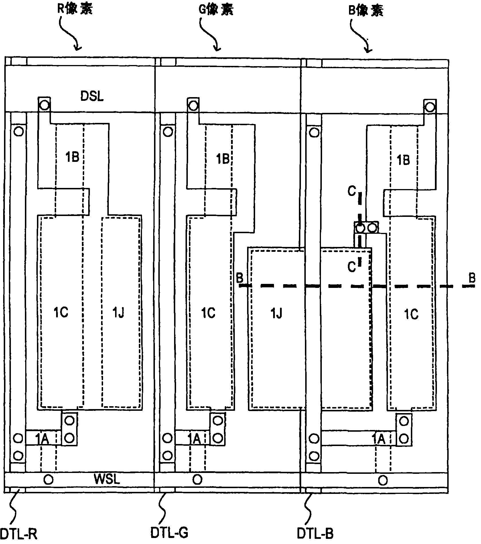
图7是图示出相关技术中的像素结构的示意平面图。图7表示R(红)像素、G(绿)像素和B(蓝)像素的布置配置。各个像素被配置在在水平方向(示图中的水平方向)上延伸的电源线DSL和扫描线WSL之间,并且RGB像素的区域被在垂直方向(示图中的垂直方向)上延伸的信号线DTL划分开。FIG. 7 is a schematic plan view illustrating a pixel structure in the related art. FIG. 7 shows an arrangement configuration of R (red) pixels, G (green) pixels, and B (blue) pixels. Each pixel is arranged between a power supply line DSL and a scanning line WSL extending in the horizontal direction (horizontal direction in the diagram), and the area of the RGB pixels is divided by signal signals extending in the vertical direction (vertical direction in the diagram). Line DTL is divided.
在每个像素的区域内,布置写晶体管1A、驱动晶体管1B和保持电容器1C。此外,还布置用于调节写增益或迁移率校正时间的辅助电容器1J。In the area of each pixel, a
在图7中所表示的示例中,示出G(绿)像素的图案密度(pattern density)低于R(红)像素的图案密度并且B(蓝)像素的图案密度高于R(红)像素的图案密度的情况。In the example represented in FIG. 7 , it is shown that the pattern density of G (green) pixels is lower than that of R (red) pixels and that of B (blue) pixels is higher than that of R (red) pixels. The case of the pattern density.
以从外部光反射的角度来看相等的间距来布置信号线DTL-R、DTL-G和DTL_B。因此,作为B(蓝)像素的构成元件的辅助电容器1J被配置为设置在相邻G(绿)像素的区域中。The signal lines DTL-R, DTL-G, and DTL_B are arranged at equal intervals from the viewpoint of external light reflection. Therefore, the
这里,写晶体管1A、驱动晶体管1B的栅极、与该栅极导通的保持电容器1C的下侧电极和与有机EL元件的阴极导通的辅助电容器1J的下侧电极形成第一布线层。Here, the gate of the
电源线DSL、信号线DTL和扫描线WSL形成第二布线层。此外,电源线DSL与信号线DTL交叉部分和信号线DTL与扫描线WSL的交叉部分通过接触孔切换到第一布线层。The power supply line DSL, the signal line DTL, and the scan line WSL form a second wiring layer. In addition, a crossing portion of the power supply line DSL and the signal line DTL and a crossing portion of the signal line DTL and the scanning line WSL are switched to the first wiring layer through the contact hole.
此外,写晶体管1A、驱动晶体管1B的源极和漏极、与驱动晶体管1B的源极(有机EL元件的阳极)导通的保持电容器1C的上侧电极以及辅助电容器1J的上侧电极由多晶硅形成。多晶硅是布置在第一布线层和第二布线层之间的中间层。In addition, the source and drain of the
图8是沿图7中所示的A-A线得到的示意横截面图。该像素结构包括第一布线层M1、第二布线层M2和由布置在玻璃基板上的多晶硅形成的中间层MD。如上所述,B(蓝)像素的辅助电容器1J的一部分被设置在相邻G(绿)像素的区域中。因此,在信号线DTL-B下面,布置由多晶硅形成的辅助电容器1J的上侧电极D1,此外,由于上侧电极D1是与B(蓝)像素的保持电容器1C的上侧电极相同的节点,所以,与B(蓝)像素的保持电容器1C的上侧电极公共地布置上侧电极D1。Fig. 8 is a schematic cross-sectional view taken along line A-A shown in Fig. 7 . The pixel structure includes a first wiring layer M1, a second wiring layer M2, and a middle layer MD formed of polysilicon disposed on a glass substrate. As described above, a part of the
等价电路Equivalent circuit
图9是图7中所表示的像素结构的像素单元的等价电路。信号线DTL连接到写晶体管1A,并且写晶体管1A的源极或漏极连接到驱动晶体管1B的栅极(节点g)。FIG. 9 is an equivalent circuit of a pixel unit of the pixel structure shown in FIG. 7 . The signal line DTL is connected to the
电源线DSL连接到驱动晶体管1B的漏极,并且保持电容器1C连接在栅极和源极之间。驱动晶体管1B的源极连接到有机EL元件1D的阳极。此外,辅助电容器1J连接在有机EL元件1D的阳极和阴极之间。A power supply line DSL is connected to the drain of the driving
在上述电路中,被配置为第二布线层的信号线DTL和被配置为中间层的、由多晶硅形成的有机EL元件1D的阳极(节点s)形成平行板电容器,从而在这形成寄生电容Cp。In the above circuit, the signal line DTL configured as the second wiring layer and the anode (node s) of the
定时图timing diagram
图10是图示出图9中所表示的电路图的操作的定时图。在该示图中,点线表示的波形表示原来的电位变动,实线表示与图9中所表示的电路图对应的电位变动。FIG. 10 is a timing diagram illustrating the operation of the circuit diagram represented in FIG. 9 . In this diagram, the waveform indicated by the dotted line indicates the original potential variation, and the solid line indicates the potential variation corresponding to the circuit diagram shown in FIG. 9 .
在图9中所表示的电路图中,在信号线DTL与阳极(节点s)之间形成寄生电容Cp。因此,当信号线DTL的电位被切换时,电容耦合在阳极(即,驱动晶体管1B的源极(节点s))重叠。In the circuit diagram shown in FIG. 9, a parasitic capacitance Cp is formed between the signal line DTL and the anode (node s). Therefore, when the potential of the signal line DTL is switched, capacitive coupling overlaps at the anode (ie, the source (node s) of the driving
在时段(I)中,当信号线DTL在视频信号采样前从信号线基准电位Vo切换成视频信号Vsig时,在信号线DTL与阳极(节点s)之间发生电容耦合。因此,驱动晶体管1B的源极(节点s)的电位从阈值校正完成后的电位上升与电容比相对应的量。类似地,根据驱动晶体管1B的源极的电位的上升,由于自举操作,驱动晶体管1B的栅极(节点g)的电位也从视频信号基准电位Vo上升。In the period (I), when the signal line DTL is switched from the signal line reference potential Vo to the video signal Vsig before video signal sampling, capacitive coupling occurs between the signal line DTL and the anode (node s). Therefore, the potential of the source (node s) of the driving
接着,在电位被升高的状态中开始对视频信号的采样。因此,不是原来的输入幅度“Vin=Vsig-Vo”而是输入幅度“Vin=Vsig-Va”(这里,Va>Vo)被输入。因此,驱动晶体管1B的栅极至源极电压下降,从而亮度降低。由于在电流流经有机EL元件1D的状态中发生时段(II)期间的电容耦合,所以,该电容耦合后,电位回到其原来的电位。Next, sampling of the video signal starts in a state where the potential is raised. Therefore, not the original input amplitude "Vin=Vsig-Vo" but the input amplitude "Vin=Vsig-Va" (here, Va>Vo) is input. Therefore, the gate-to-source voltage of the driving
3.该实施例的配置示例3. Configuration example of this embodiment
系统配置System Configuration
图11是表示该实施例的一个示例的系统配置的示图。如图11中所示,有机EL显示装置100具有这样的配置,其包括通过以矩阵形状二维地布置像素(PXLC)101形成的像素阵列单元102以及被布置在像素阵列单元102的外围并且驱动各个像素101的驱动单元。例如,布置水平驱动电路103、写扫描电路104和电源扫描电路105作为驱动像素101的驱动单元。FIG. 11 is a diagram showing a system configuration of one example of this embodiment. As shown in FIG. 11 , an organic
在像素阵列单元102中,在具有m行和n列的像素阵列中,为每个像素行配置扫描线WSL-1至WSL-m和电源线DSL-1至DSL-m,并且为每个像素列配置信号线DTL-1至DTL-n。这些组件的配置与图1中所表示的相同。In the
布线结构wiring structure
图12是图示出根据该实施例的像素结构的示意平面图。图12表示R(红)像素、G(绿)像素和B(蓝)像素的布置配置。各个像素被配置在在水平方向(示图中的水平方向)上延伸的电源线DSL和扫描线WSL之间,并且RGB像素的区域被在垂直方向(示图中的垂直方向)上延伸的信号线DTL划分开。FIG. 12 is a schematic plan view illustrating a pixel structure according to this embodiment. FIG. 12 shows an arrangement configuration of R (red) pixels, G (green) pixels, and B (blue) pixels. Each pixel is arranged between a power supply line DSL and a scanning line WSL extending in the horizontal direction (horizontal direction in the diagram), and the area of the RGB pixels is divided by signal signals extending in the vertical direction (vertical direction in the diagram). Line DTL is divided.
在每个像素的区域内,布置写晶体管1A、驱动晶体管1B和保持电容器1C。此外,还布置用于调节写增益或迁移率校正时间的辅助电容器1J。In the area of each pixel, a
在图12中所表示的示例中,示出G(绿)像素的图案密度低于R(红)像素的图案密度并且B(蓝)像素的图案密度高于R(红)像素的图案密度的情况。In the example represented in FIG. 12 , it is shown that the pattern density of G (green) pixels is lower than that of R (red) pixels and the pattern density of B (blue) pixels is higher than that of R (red) pixels. Condition.
以从外部光发射的角度来看相等的间距来布置信号线DTL-R、DTL-G和DTL_B。因此,作为B(蓝)像素的构成元件的辅助电容器1J被配置为设置在相邻G(绿)像素的区域中。The signal lines DTL-R, DTL-G, and DTL_B are arranged at equal intervals from the viewpoint of external light emission. Therefore, the
这里,写晶体管1A、驱动晶体管1B的栅极、与该栅极导通的保持电容器1C的下侧电极和辅助电容器1J的下侧电极形成第一布线层。Here, the gate of the
此外,电源线DSL、信号线DTL和扫描线WSL形成第二布线层。此外,电源线DSL与信号线DTL交叉部分和信号线DTL与扫描线WSL的交叉部分通过接触孔切换到第一布线层。In addition, the power supply line DSL, the signal line DTL, and the scan line WSL form a second wiring layer. In addition, a crossing portion of the power supply line DSL and the signal line DTL and a crossing portion of the signal line DTL and the scanning line WSL are switched to the first wiring layer through the contact hole.
此外,写晶体管1A、驱动晶体管1B的源极和漏极、与驱动晶体管1B的源极导通的保持电容器1C的上侧电极以及辅助电容器1J的上侧电极由多晶硅形成。多晶硅是布置在第一布线层和第二布线层之间的中间层。Further, the source and drain of the
在上述布线配置中,根据该实施例,辅助电容器1J的上侧电极(一个电极)与有机EL元件的阴极被使得相互导通,并且辅助电容器1J的下侧电极(另一个电极)与有机EL元件的阳极被使得相互导通。In the above wiring configuration, according to this embodiment, the upper electrode (one electrode) of the
换而言之,在根据该实施例的像素结构的图案布局中,当辅助电容器1J经过信号线DTL的下侧时,辅助电容器1J的被布置在信号线DTL侧的上侧电极(一个电极)被使得与驱动晶体管1B的源极(有机EL元件1D的阳极(节点s))导通,并且被设置为第一布线层。此外,辅助电容器1J的下侧电极(另一个电极)被使得与有机EL元件1D的阴极1H导通并且被设置为由多晶硅形成的中间层。In other words, in the pattern layout of the pixel structure according to this embodiment, when the
图13是沿图12中所示的B-B线得到的示意横截面图。该像素结构包括第一布线层M1、第二布线层M2和由布置在玻璃基板上的多晶硅形成的中间层MD。如上所述,B(蓝)像素的辅助电容器1J的一部分被设置在相邻G(绿)像素的区域中。因此,在信号线DTL-B下面,布置由多晶硅形成的辅助电容器1J的上侧电极D1-1J。此外,在由多晶硅形成的中间层MD中,布置B(蓝)像素的保持电容器1C的上侧电极D1-1C。Fig. 13 is a schematic cross-sectional view taken along line B-B shown in Fig. 12 . The pixel structure includes a first wiring layer M1, a second wiring layer M2, and a middle layer MD formed of polysilicon disposed on a glass substrate. As described above, a part of the
在上述横截面结构中,根据该实施例,辅助电容器1J的上侧电极D1-1J被使得与有机EL元件的阴极导通,并且下侧电极D2-1J被使得与阳极导通。In the above cross-sectional structure, according to this embodiment, the upper side electrode D1-1J of the
图14是沿图12中所示的C-C线得到的示意横截面图。根据该实施例,辅助电容器1J的上侧电极D1-1J的节点和保持电容器1C的上侧电极D1-1C的节点不同并且相互分离。此外,辅助电容器1J的下侧电极D2-1J的节点和保持电容器1C的上侧电极D1-1C的节点相同并且相互导通。为了使得这些电极相互导通,在辅助电容器1J的下侧电极D2-1J中形成接触孔CH1,并且在保持电容器1C的上侧电极D1-1C中形成接触孔CH2,并且辅助电容器1J的下侧电极D2-1J和保持电容器1C的上侧电极D1-1C通过被布置在第二布线层中的布线D2来相互连接而导通。Fig. 14 is a schematic cross-sectional view taken along line C-C shown in Fig. 12 . According to this embodiment, the node of the upper electrode D1 - 1J of the
通过使用上述布线结构,即使辅助电容器1J被配置为经过信号线DTL-B下面,也可以通过阴极1H在信号线DTL-B和阳极(节点s)之间构成屏蔽。因此,在信号线DTL-B和辅助电容器1J的阳极侧电极之间不形成如图9中所表示的寄生电容Cp。By using the above wiring structure, even if the
定时图timing diagram
图15是图示出根据该实施例的像素配置的操作的定时图。在该示图中,实线表示该实施例的像素配置中的电位变动,并且点线表示包括图4A至图4D的电路示图中所表示的寄生电容Cp的情况中的电位变动。FIG. 15 is a timing chart illustrating the operation of the pixel configuration according to this embodiment. In this diagram, the solid line indicates the potential variation in the pixel configuration of this embodiment, and the dotted line indicates the potential variation in the case of including the parasitic capacitance Cp shown in the circuit diagrams of FIGS. 4A to 4D .
在包括寄生电容Cp的情况中,当视频线DTL的电位被切换时,电容耦合在阳极,即,驱动晶体管1B的源极(节点s)重叠。在时段(I)中,当信号线DTL在视频信号采样前从视频信号线基准电位Vo切换成视频信号Vsig时,在信号线DTL与阳极(节点s)之间发生电容耦合。因此,驱动晶体管1B的源极(节点s)的电位从阈值校正完成后的电位上升与电容比相对应的量。类似地,根据驱动晶体管1B的源极的电位的上升,由于自举操作,N型驱动晶体管1B的栅极g的电位也从视频信号线基准电位Vo上升。In the case where the parasitic capacitance Cp is included, when the potential of the video line DTL is switched, capacitive coupling overlaps at the anode, that is, the source (node s) of the driving
接着,在电位被升高的状态中开始对视频信号的采样。因此,不是原来的输入幅度“Vin=Vsig-Vo”而是输入幅度“Vin=Vsig-Va”(这里,Va>Vo)被输入。因此,N型驱动晶体管1B的栅极至源极电压下降,从而亮度降低。Next, sampling of the video signal starts in a state where the potential is raised. Therefore, not the original input amplitude "Vin=Vsig-Vo" but the input amplitude "Vin=Vsig-Va" (here, Va>Vo) is input. Therefore, the gate-to-source voltage of the N-
另一方面,根据该实施例,不形成寄生电容Cp。因此,当视频信号线DTL的电位被切换时,电容耦合不在驱动晶体管1B的源极(节点s)重叠。因此,驱动晶体管1B的源极(节点s)在阈值校正完成后不改变。因此,对视频信号的采样是在阈值被校正的状态中开始的,并且因此,原来的输入幅度“Vin=Vsig-Vo”被输入,从而很少发生亮度降低。On the other hand, according to this embodiment, no parasitic capacitance Cp is formed. Therefore, when the potential of the video signal line DTL is switched, capacitive coupling does not overlap at the source (node s) of the driving
在上述实施例中,已经描述了本发明应用于使用有机EL元件作为图11中所表示的像素101的电光元件的有机EL显示装置的情况作为示例。然而,本发明不限于这样的应用,并且可以应用于所有使用发光亮度随流经装置的电流值而改变的电流驱动型电光元件(发光元件)的显示装置。In the above-described embodiments, the case where the present invention is applied to an organic EL display device using an organic EL element as an electro-optical element of the
此外,已经描述了将包括两个晶体管(Tr)和一个电容器(C)的2Tr/1C像素配置用作像素101的配置来作为示例。然而,本发明不限于此。因此,本发明可以适用于不同的像素配置,例如,包括四个晶体管(Tr)和一个电容器(C)的4Tr/1C像素配置。Furthermore, the configuration using a 2Tr/1C pixel configuration including two transistors (Tr) and one capacitor (C) as the
4.应用例4. Application example
根据该实施例的上述显示装置可以适用于例如如图15至图19所表示的各种电子设备。例如,上述显示装置可以用作所有领域的电子设备的显示装置,其中输入电子设备的视频信号或电子设备中所生成的视频信号被显示为图像或视频,所述电子设备例如是数字相机,笔记本电脑、包括蜂窝电话等的移动终端以及视频相机。The above-mentioned display device according to this embodiment can be applied to various electronic devices as shown in FIGS. 15 to 19 , for example. For example, the display device described above can be used as a display device of electronic equipment in all fields in which video signals input to electronic equipment or video signals generated in electronic equipment, such as digital cameras, notebooks, etc., are displayed as images or videos. Computers, mobile terminals including cellular phones, etc., and video cameras.
如上所述,通过使用根据该实施例的显示装置作为所有领域的电子设备的显示装置,可以提高显示图像的图像质量。因此,具有在各种电子设备中执行高质量图像显示的优点。As described above, by using the display device according to this embodiment as a display device of electronic equipment in all fields, the image quality of a displayed image can be improved. Therefore, there is an advantage of performing high-quality image display in various electronic devices.
此外,根据该实施例的显示装置包括具有模块形状的密封配置的显示装置。例如,通过被附着到像素阵列单元102的相对部分(例如,透明玻璃之类)而形成的显示模块对应于这样的显示装置。在该透明的相对部分中,可以布置色彩过滤器、保护膜等,并且另外还可以布置上述遮光膜。此外,在该显示模块中,可以布置FPC(软式印刷电路板)、用于从外部向像素阵列单元输入或输出信号等的电路单元等。Furthermore, the display device according to this embodiment includes a display device having a module-shaped sealing configuration. For example, a display module formed by being attached to an opposite portion of the pixel array unit 102 (for example, transparent glass or the like) corresponds to such a display device. In this transparent opposite portion, a color filter, a protective film, etc. may be arranged, and in addition, the above-mentioned light-shielding film may also be arranged. Further, in the display module, an FPC (Flexible Printed Circuit Board), a circuit unit for inputting or outputting a signal or the like from the outside to the pixel array unit, and the like may be arranged.
以下,将描述应用根据本该实施例的显示装置的电子设备的具体示例。Hereinafter, a specific example of electronic equipment to which the display device according to this embodiment is applied will be described.
图16是示出应用了该实施例的电视机的外观的透视图。根据该应用例的电视机包括由前置面板108、滤光玻璃109等构成的视频显示屏单元107。通过使用根据该实施例的显示装置作为视频显示屏单元107来配置电视机。Fig. 16 is a perspective view showing the appearance of a television to which this embodiment is applied. The television set according to this application example includes a video display screen unit 107 constituted by a front panel 108, a filter glass 109, and the like. A television is configured by using the display device according to this embodiment as the video display screen unit 107 .
图17A和图17B是示出应用了该实施例的数字相机的外观的透视图。图17A是从前面看到的视图,并且图17B是从后面看到的视图。根据该应用例的数字相机包括用于闪光灯的发光单元111、显示单元112、菜单开关113、快门按钮114等等。该数字相机是通过使用根据该实施例的显示装置作为显示单元112来制造的。17A and 17B are perspective views showing the appearance of a digital camera to which this embodiment is applied. FIG. 17A is a view seen from the front, and FIG. 17B is a view seen from the rear. The digital camera according to this application example includes a
图18是示出应用了该实施例的笔记本电脑的外观的透视图。根据该实施例的笔记本电脑包括当文本等被输入主体121时所操作的键盘122、显示图像的显示单元123等等。该笔记本电脑是通过使用根据该实施例的显示装置作为显示单元123来制造的。FIG. 18 is a perspective view showing the appearance of a notebook computer to which this embodiment is applied. The notebook computer according to this embodiment includes a
图19是示出应用了该实施例的视频相机的外观的透视图。根据该实施例的视频相机包括主体单元131、被布置在面向拍摄对象的前侧的那一侧上的镜头132、用于拍摄的开始/停止开关133、显示单元134等等。该视频相机是通过使用根据该实施例的显示装置作为显示单元134来制造的。FIG. 19 is a perspective view showing the appearance of a video camera to which this embodiment is applied. The video camera according to this embodiment includes a
图20A至图20G是示出应用了该实施例的移动终端装置(例如,蜂窝电话)的外观的示图,图20A是其打开状态的正视图,图20B是其左视图,图20C是闭合状态的正视图,图20D是左视图,图20E是右视图,图20F是仰视图,图20G是俯视图。根据该应用例的蜂窝电话包括上侧壳体141、下侧壳体142、连接部件(例如,铰链部件)143、显示器144、子显示器145、图画灯146、相机147等。该蜂窝电话是通过使用根据该实施例的显示装置作为显示器144或子显示器145来制造的。20A to 20G are diagrams showing the appearance of a mobile terminal device (for example, a cellular phone) to which this embodiment is applied, FIG. 20A is a front view of its open state, FIG. 20B is a left side view thereof, and FIG. 20C is a closed state. The front view of the state, FIG. 20D is a left view, FIG. 20E is a right view, FIG. 20F is a bottom view, and FIG. 20G is a top view. The cellular phone according to this application example includes an
本申请包含与2009年1月16日在日本专利局提交的日本优先专利申请JP 2009-007344中所公开的主题有关的主题,其全部内容通过引用被结合于此。The present application contains subject matter related to that disclosed in Japanese Priority Patent Application JP 2009-007344 filed in the Japan Patent Office on Jan. 16, 2009, the entire content of which is hereby incorporated by reference.
本领域技术人员应当理解,根据设计要求和其它因素可以进行各种修改、组合、子组合和更改,只要它们在所附权利要求及其等同物的范围内即可。It should be understood by those skilled in the art that various modifications, combinations, sub-combinations and alterations may occur depending on design requirements and other factors insofar as they are within the scope of the appended claims and the equivalents thereof.
Claims (4)
Applications Claiming Priority (2)
| Application Number | Priority Date | Filing Date | Title |
|---|---|---|---|
| JP2009007344A JP5304257B2 (en) | 2009-01-16 | 2009-01-16 | Display device and electronic device |
| JP2009-007344 | 2009-01-16 |
Publications (2)
| Publication Number | Publication Date |
|---|---|
| CN101783361A CN101783361A (en) | 2010-07-21 |
| CN101783361B true CN101783361B (en) | 2012-03-14 |
Family
ID=42061932
Family Applications (1)
| Application Number | Title | Priority Date | Filing Date |
|---|---|---|---|
| CN2010100040373A Expired - Fee Related CN101783361B (en) | 2009-01-16 | 2010-01-18 | Display device and electronic apparatus |
Country Status (6)
| Country | Link |
|---|---|
| US (2) | US8368073B2 (en) |
| EP (1) | EP2209106A1 (en) |
| JP (1) | JP5304257B2 (en) |
| KR (1) | KR101504780B1 (en) |
| CN (1) | CN101783361B (en) |
| TW (1) | TWI416469B (en) |
Families Citing this family (12)
| Publication number | Priority date | Publication date | Assignee | Title |
|---|---|---|---|---|
| KR101962850B1 (en) * | 2011-04-22 | 2019-03-28 | 삼성디스플레이 주식회사 | An organic light emitting display device and the manufacturing method thereof |
| JP5686043B2 (en) * | 2011-06-02 | 2015-03-18 | セイコーエプソン株式会社 | Electro-optical device and electronic apparatus |
| JP6012450B2 (en) | 2011-12-23 | 2016-10-25 | 株式会社半導体エネルギー研究所 | Driving method of semiconductor device |
| KR102081910B1 (en) * | 2013-06-12 | 2020-02-27 | 삼성디스플레이 주식회사 | Capacitor, driving circuit comprising the capacitor, and display device comprising the driving circuit |
| JP6330220B2 (en) * | 2014-03-27 | 2018-05-30 | 株式会社Joled | Display device, electronic device and substrate |
| WO2016013264A1 (en) | 2014-07-23 | 2016-01-28 | ソニー株式会社 | Display device, method for manufacturing display device, and electronic device |
| KR102367462B1 (en) * | 2015-08-11 | 2022-02-25 | 삼성디스플레이 주식회사 | Organic light emitting diode display device |
| KR101937768B1 (en) * | 2016-12-01 | 2019-01-11 | 엘지디스플레이 주식회사 | Organic light emitting display device |
| KR102585451B1 (en) * | 2016-12-27 | 2023-10-06 | 삼성디스플레이 주식회사 | Light emitting display device |
| KR102460917B1 (en) * | 2017-12-13 | 2022-10-28 | 엘지디스플레이 주식회사 | Display Device |
| CN114335028B (en) * | 2018-08-10 | 2025-07-29 | 友达光电股份有限公司 | Display device |
| CN110491343A (en) * | 2019-08-30 | 2019-11-22 | 昆山国显光电有限公司 | OLED pixel structure and display device |
Family Cites Families (13)
| Publication number | Priority date | Publication date | Assignee | Title |
|---|---|---|---|---|
| JP3757797B2 (en) * | 2001-01-09 | 2006-03-22 | 株式会社日立製作所 | Organic LED display and driving method thereof |
| JP4529467B2 (en) | 2004-02-13 | 2010-08-25 | ソニー株式会社 | Pixel circuit and display device |
| JP4873882B2 (en) * | 2004-05-21 | 2012-02-08 | 三洋電機株式会社 | Liquid crystal display |
| JP2006133542A (en) | 2004-11-08 | 2006-05-25 | Sony Corp | Pixel circuit and display device |
| CA2490858A1 (en) * | 2004-12-07 | 2006-06-07 | Ignis Innovation Inc. | Driving method for compensated voltage-programming of amoled displays |
| JP4923505B2 (en) * | 2005-10-07 | 2012-04-25 | ソニー株式会社 | Pixel circuit and display device |
| JP4203773B2 (en) * | 2006-08-01 | 2009-01-07 | ソニー株式会社 | Display device |
| TWI389081B (en) * | 2007-01-26 | 2013-03-11 | Sony Corp | Display device, driving method of the same and electronic equipment having the same |
| JP2008233399A (en) * | 2007-03-19 | 2008-10-02 | Sony Corp | Pixel circuit, display device, and manufacturing method of display device |
| JP4306753B2 (en) * | 2007-03-22 | 2009-08-05 | ソニー株式会社 | Display device, driving method thereof, and electronic apparatus |
| JP2008257086A (en) * | 2007-04-09 | 2008-10-23 | Sony Corp | Display device, display device manufacturing method, and electronic apparatus |
| JP4428436B2 (en) | 2007-10-23 | 2010-03-10 | ソニー株式会社 | Display device and electronic device |
| JP4614106B2 (en) | 2008-06-18 | 2011-01-19 | ソニー株式会社 | Self-luminous display device and electronic device |
-
2009
- 2009-01-16 JP JP2009007344A patent/JP5304257B2/en not_active Expired - Fee Related
- 2009-12-24 TW TW098144790A patent/TWI416469B/en not_active IP Right Cessation
- 2009-12-30 EP EP09180994A patent/EP2209106A1/en not_active Withdrawn
-
2010
- 2010-01-08 KR KR1020100001564A patent/KR101504780B1/en not_active Expired - Fee Related
- 2010-01-12 US US12/655,974 patent/US8368073B2/en not_active Expired - Fee Related
- 2010-01-18 CN CN2010100040373A patent/CN101783361B/en not_active Expired - Fee Related
-
2012
- 2012-12-27 US US13/727,768 patent/US20130113689A1/en not_active Abandoned
Also Published As
| Publication number | Publication date |
|---|---|
| KR101504780B1 (en) | 2015-03-20 |
| US8368073B2 (en) | 2013-02-05 |
| US20130113689A1 (en) | 2013-05-09 |
| TWI416469B (en) | 2013-11-21 |
| KR20100084471A (en) | 2010-07-26 |
| JP2010164801A (en) | 2010-07-29 |
| US20100182224A1 (en) | 2010-07-22 |
| EP2209106A1 (en) | 2010-07-21 |
| TW201042614A (en) | 2010-12-01 |
| JP5304257B2 (en) | 2013-10-02 |
| CN101783361A (en) | 2010-07-21 |
Similar Documents
| Publication | Publication Date | Title |
|---|---|---|
| US11004390B2 (en) | Display device and electronic apparatus | |
| CN101783361B (en) | Display device and electronic apparatus | |
| US8736521B2 (en) | Display device and electronic apparatus have the same | |
| US9847384B2 (en) | Display device, method for driving the same, and electronic apparatus | |
| KR101567734B1 (en) | Display device and electronic equipment | |
| US20140204004A1 (en) | Display device with power source supply scan circuits conducting negative feedback and driving method thereof | |
| TWI413067B (en) | Display, method of driving display, and electronic device |
Legal Events
| Date | Code | Title | Description |
|---|---|---|---|
| C06 | Publication | ||
| PB01 | Publication | ||
| C10 | Entry into substantive examination | ||
| SE01 | Entry into force of request for substantive examination | ||
| C14 | Grant of patent or utility model | ||
| GR01 | Patent grant | ||
| CF01 | Termination of patent right due to non-payment of annual fee | ||
| CF01 | Termination of patent right due to non-payment of annual fee |
Granted publication date: 20120314 |