CN101772833B - gas supply device - Google Patents
gas supply device Download PDFInfo
- Publication number
- CN101772833B CN101772833B CN2009801000561A CN200980100056A CN101772833B CN 101772833 B CN101772833 B CN 101772833B CN 2009801000561 A CN2009801000561 A CN 2009801000561A CN 200980100056 A CN200980100056 A CN 200980100056A CN 101772833 B CN101772833 B CN 101772833B
- Authority
- CN
- China
- Prior art keywords
- gas
- gas supply
- mentioned
- processing
- substrate
- Prior art date
- Legal status (The legal status is an assumption and is not a legal conclusion. Google has not performed a legal analysis and makes no representation as to the accuracy of the status listed.)
- Active
Links
Images


Classifications
-
- C—CHEMISTRY; METALLURGY
- C23—COATING METALLIC MATERIAL; COATING MATERIAL WITH METALLIC MATERIAL; CHEMICAL SURFACE TREATMENT; DIFFUSION TREATMENT OF METALLIC MATERIAL; COATING BY VACUUM EVAPORATION, BY SPUTTERING, BY ION IMPLANTATION OR BY CHEMICAL VAPOUR DEPOSITION, IN GENERAL; INHIBITING CORROSION OF METALLIC MATERIAL OR INCRUSTATION IN GENERAL
- C23C—COATING METALLIC MATERIAL; COATING MATERIAL WITH METALLIC MATERIAL; SURFACE TREATMENT OF METALLIC MATERIAL BY DIFFUSION INTO THE SURFACE, BY CHEMICAL CONVERSION OR SUBSTITUTION; COATING BY VACUUM EVAPORATION, BY SPUTTERING, BY ION IMPLANTATION OR BY CHEMICAL VAPOUR DEPOSITION, IN GENERAL
- C23C16/00—Chemical coating by decomposition of gaseous compounds, without leaving reaction products of surface material in the coating, i.e. chemical vapour deposition [CVD] processes
- C23C16/44—Chemical coating by decomposition of gaseous compounds, without leaving reaction products of surface material in the coating, i.e. chemical vapour deposition [CVD] processes characterised by the method of coating
- C23C16/455—Chemical coating by decomposition of gaseous compounds, without leaving reaction products of surface material in the coating, i.e. chemical vapour deposition [CVD] processes characterised by the method of coating characterised by the method used for introducing gases into reaction chamber or for modifying gas flows in reaction chamber
- C23C16/45523—Pulsed gas flow or change of composition over time
- C23C16/45525—Atomic layer deposition [ALD]
- C23C16/45544—Atomic layer deposition [ALD] characterized by the apparatus
-
- C—CHEMISTRY; METALLURGY
- C23—COATING METALLIC MATERIAL; COATING MATERIAL WITH METALLIC MATERIAL; CHEMICAL SURFACE TREATMENT; DIFFUSION TREATMENT OF METALLIC MATERIAL; COATING BY VACUUM EVAPORATION, BY SPUTTERING, BY ION IMPLANTATION OR BY CHEMICAL VAPOUR DEPOSITION, IN GENERAL; INHIBITING CORROSION OF METALLIC MATERIAL OR INCRUSTATION IN GENERAL
- C23C—COATING METALLIC MATERIAL; COATING MATERIAL WITH METALLIC MATERIAL; SURFACE TREATMENT OF METALLIC MATERIAL BY DIFFUSION INTO THE SURFACE, BY CHEMICAL CONVERSION OR SUBSTITUTION; COATING BY VACUUM EVAPORATION, BY SPUTTERING, BY ION IMPLANTATION OR BY CHEMICAL VAPOUR DEPOSITION, IN GENERAL
- C23C16/00—Chemical coating by decomposition of gaseous compounds, without leaving reaction products of surface material in the coating, i.e. chemical vapour deposition [CVD] processes
- C23C16/22—Chemical coating by decomposition of gaseous compounds, without leaving reaction products of surface material in the coating, i.e. chemical vapour deposition [CVD] processes characterised by the deposition of inorganic material, other than metallic material
- C23C16/30—Deposition of compounds, mixtures or solid solutions, e.g. borides, carbides, nitrides
- C23C16/40—Oxides
- C23C16/409—Oxides of the type ABO3 with A representing alkali, alkaline earth metal or lead and B representing a refractory metal, nickel, scandium or a lanthanide
-
- C—CHEMISTRY; METALLURGY
- C23—COATING METALLIC MATERIAL; COATING MATERIAL WITH METALLIC MATERIAL; CHEMICAL SURFACE TREATMENT; DIFFUSION TREATMENT OF METALLIC MATERIAL; COATING BY VACUUM EVAPORATION, BY SPUTTERING, BY ION IMPLANTATION OR BY CHEMICAL VAPOUR DEPOSITION, IN GENERAL; INHIBITING CORROSION OF METALLIC MATERIAL OR INCRUSTATION IN GENERAL
- C23C—COATING METALLIC MATERIAL; COATING MATERIAL WITH METALLIC MATERIAL; SURFACE TREATMENT OF METALLIC MATERIAL BY DIFFUSION INTO THE SURFACE, BY CHEMICAL CONVERSION OR SUBSTITUTION; COATING BY VACUUM EVAPORATION, BY SPUTTERING, BY ION IMPLANTATION OR BY CHEMICAL VAPOUR DEPOSITION, IN GENERAL
- C23C16/00—Chemical coating by decomposition of gaseous compounds, without leaving reaction products of surface material in the coating, i.e. chemical vapour deposition [CVD] processes
- C23C16/44—Chemical coating by decomposition of gaseous compounds, without leaving reaction products of surface material in the coating, i.e. chemical vapour deposition [CVD] processes characterised by the method of coating
- C23C16/455—Chemical coating by decomposition of gaseous compounds, without leaving reaction products of surface material in the coating, i.e. chemical vapour deposition [CVD] processes characterised by the method of coating characterised by the method used for introducing gases into reaction chamber or for modifying gas flows in reaction chamber
- C23C16/45502—Flow conditions in reaction chamber
- C23C16/45508—Radial flow
-
- C—CHEMISTRY; METALLURGY
- C23—COATING METALLIC MATERIAL; COATING MATERIAL WITH METALLIC MATERIAL; CHEMICAL SURFACE TREATMENT; DIFFUSION TREATMENT OF METALLIC MATERIAL; COATING BY VACUUM EVAPORATION, BY SPUTTERING, BY ION IMPLANTATION OR BY CHEMICAL VAPOUR DEPOSITION, IN GENERAL; INHIBITING CORROSION OF METALLIC MATERIAL OR INCRUSTATION IN GENERAL
- C23C—COATING METALLIC MATERIAL; COATING MATERIAL WITH METALLIC MATERIAL; SURFACE TREATMENT OF METALLIC MATERIAL BY DIFFUSION INTO THE SURFACE, BY CHEMICAL CONVERSION OR SUBSTITUTION; COATING BY VACUUM EVAPORATION, BY SPUTTERING, BY ION IMPLANTATION OR BY CHEMICAL VAPOUR DEPOSITION, IN GENERAL
- C23C16/00—Chemical coating by decomposition of gaseous compounds, without leaving reaction products of surface material in the coating, i.e. chemical vapour deposition [CVD] processes
- C23C16/44—Chemical coating by decomposition of gaseous compounds, without leaving reaction products of surface material in the coating, i.e. chemical vapour deposition [CVD] processes characterised by the method of coating
- C23C16/455—Chemical coating by decomposition of gaseous compounds, without leaving reaction products of surface material in the coating, i.e. chemical vapour deposition [CVD] processes characterised by the method of coating characterised by the method used for introducing gases into reaction chamber or for modifying gas flows in reaction chamber
- C23C16/45523—Pulsed gas flow or change of composition over time
- C23C16/45525—Atomic layer deposition [ALD]
- C23C16/45527—Atomic layer deposition [ALD] characterized by the ALD cycle, e.g. different flows or temperatures during half-reactions, unusual pulsing sequence, use of precursor mixtures or auxiliary reactants or activations
- C23C16/45531—Atomic layer deposition [ALD] characterized by the ALD cycle, e.g. different flows or temperatures during half-reactions, unusual pulsing sequence, use of precursor mixtures or auxiliary reactants or activations specially adapted for making ternary or higher compositions
-
- C—CHEMISTRY; METALLURGY
- C23—COATING METALLIC MATERIAL; COATING MATERIAL WITH METALLIC MATERIAL; CHEMICAL SURFACE TREATMENT; DIFFUSION TREATMENT OF METALLIC MATERIAL; COATING BY VACUUM EVAPORATION, BY SPUTTERING, BY ION IMPLANTATION OR BY CHEMICAL VAPOUR DEPOSITION, IN GENERAL; INHIBITING CORROSION OF METALLIC MATERIAL OR INCRUSTATION IN GENERAL
- C23C—COATING METALLIC MATERIAL; COATING MATERIAL WITH METALLIC MATERIAL; SURFACE TREATMENT OF METALLIC MATERIAL BY DIFFUSION INTO THE SURFACE, BY CHEMICAL CONVERSION OR SUBSTITUTION; COATING BY VACUUM EVAPORATION, BY SPUTTERING, BY ION IMPLANTATION OR BY CHEMICAL VAPOUR DEPOSITION, IN GENERAL
- C23C16/00—Chemical coating by decomposition of gaseous compounds, without leaving reaction products of surface material in the coating, i.e. chemical vapour deposition [CVD] processes
- C23C16/44—Chemical coating by decomposition of gaseous compounds, without leaving reaction products of surface material in the coating, i.e. chemical vapour deposition [CVD] processes characterised by the method of coating
- C23C16/455—Chemical coating by decomposition of gaseous compounds, without leaving reaction products of surface material in the coating, i.e. chemical vapour deposition [CVD] processes characterised by the method of coating characterised by the method used for introducing gases into reaction chamber or for modifying gas flows in reaction chamber
- C23C16/45559—Diffusion of reactive gas to substrate
-
- C—CHEMISTRY; METALLURGY
- C23—COATING METALLIC MATERIAL; COATING MATERIAL WITH METALLIC MATERIAL; CHEMICAL SURFACE TREATMENT; DIFFUSION TREATMENT OF METALLIC MATERIAL; COATING BY VACUUM EVAPORATION, BY SPUTTERING, BY ION IMPLANTATION OR BY CHEMICAL VAPOUR DEPOSITION, IN GENERAL; INHIBITING CORROSION OF METALLIC MATERIAL OR INCRUSTATION IN GENERAL
- C23C—COATING METALLIC MATERIAL; COATING MATERIAL WITH METALLIC MATERIAL; SURFACE TREATMENT OF METALLIC MATERIAL BY DIFFUSION INTO THE SURFACE, BY CHEMICAL CONVERSION OR SUBSTITUTION; COATING BY VACUUM EVAPORATION, BY SPUTTERING, BY ION IMPLANTATION OR BY CHEMICAL VAPOUR DEPOSITION, IN GENERAL
- C23C16/00—Chemical coating by decomposition of gaseous compounds, without leaving reaction products of surface material in the coating, i.e. chemical vapour deposition [CVD] processes
- C23C16/44—Chemical coating by decomposition of gaseous compounds, without leaving reaction products of surface material in the coating, i.e. chemical vapour deposition [CVD] processes characterised by the method of coating
- C23C16/455—Chemical coating by decomposition of gaseous compounds, without leaving reaction products of surface material in the coating, i.e. chemical vapour deposition [CVD] processes characterised by the method of coating characterised by the method used for introducing gases into reaction chamber or for modifying gas flows in reaction chamber
- C23C16/45563—Gas nozzles
-
- C—CHEMISTRY; METALLURGY
- C23—COATING METALLIC MATERIAL; COATING MATERIAL WITH METALLIC MATERIAL; CHEMICAL SURFACE TREATMENT; DIFFUSION TREATMENT OF METALLIC MATERIAL; COATING BY VACUUM EVAPORATION, BY SPUTTERING, BY ION IMPLANTATION OR BY CHEMICAL VAPOUR DEPOSITION, IN GENERAL; INHIBITING CORROSION OF METALLIC MATERIAL OR INCRUSTATION IN GENERAL
- C23C—COATING METALLIC MATERIAL; COATING MATERIAL WITH METALLIC MATERIAL; SURFACE TREATMENT OF METALLIC MATERIAL BY DIFFUSION INTO THE SURFACE, BY CHEMICAL CONVERSION OR SUBSTITUTION; COATING BY VACUUM EVAPORATION, BY SPUTTERING, BY ION IMPLANTATION OR BY CHEMICAL VAPOUR DEPOSITION, IN GENERAL
- C23C16/00—Chemical coating by decomposition of gaseous compounds, without leaving reaction products of surface material in the coating, i.e. chemical vapour deposition [CVD] processes
- C23C16/44—Chemical coating by decomposition of gaseous compounds, without leaving reaction products of surface material in the coating, i.e. chemical vapour deposition [CVD] processes characterised by the method of coating
- C23C16/455—Chemical coating by decomposition of gaseous compounds, without leaving reaction products of surface material in the coating, i.e. chemical vapour deposition [CVD] processes characterised by the method of coating characterised by the method used for introducing gases into reaction chamber or for modifying gas flows in reaction chamber
- C23C16/45582—Expansion of gas before it reaches the substrate
Landscapes
- Chemical & Material Sciences (AREA)
- General Chemical & Material Sciences (AREA)
- Chemical Kinetics & Catalysis (AREA)
- Engineering & Computer Science (AREA)
- Materials Engineering (AREA)
- Mechanical Engineering (AREA)
- Metallurgy (AREA)
- Organic Chemistry (AREA)
- Inorganic Chemistry (AREA)
- Chemical Vapour Deposition (AREA)
- Formation Of Insulating Films (AREA)
Abstract
Description
技术领域 technical field
本发明涉及向处理容器内供给用于在该处理容器内对基板进行处理的处理气体的技术。The present invention relates to a technique of supplying a processing gas for processing a substrate in a processing container into a processing container.
背景技术 Background technique
在半导体制造装置中包括:使气体供给装置与载置台在处理容器内对置而从气体供给装置向载置于载置台上的基板即例如半导体晶片(以下简称为晶片)供给处理气体来处理基板的装置,例如成膜装置和蚀刻装置等。In a semiconductor manufacturing apparatus, a gas supply device and a mounting table are opposed to each other in a processing container, and a processing gas is supplied from the gas supply device to a substrate mounted on the mounting table, for example, a semiconductor wafer (hereinafter simply referred to as a wafer) to process the substrate. Devices, such as film forming devices and etching devices, etc.
其中作为成膜装置有加热处理气体而使其反应的热CVD装置等。并且公知有ALD(Atomic Layer Deposition:原子层沉积)或MLD(molecular Layer Deposition:分子层沉积)等工艺,即:将多种处理气体的供给分为例如两个工序(阶段),在第一工序中供给第一处理气体,在第二工序中供给第二处理气体,交替进行这些工序从而将各处理气体的反应生成物顺次层叠(例如JP特开2004-91874号公报:特别是0002段)。关于ALD,公知有从晶片的横侧流过处理气体的侧流方式。但是本发明者认为在ALD中也是从与晶片相对的方向供给气体的方向比较有利。Among them, as a film forming device, there is a thermal CVD device that heats a processing gas to cause a reaction, and the like. In addition, processes such as ALD (Atomic Layer Deposition: atomic layer deposition) or MLD (molecular Layer Deposition: molecular layer deposition) are known, that is, the supply of various processing gases is divided into two processes (stages), for example, in the first process The first process gas is supplied in the second process, and the second process gas is supplied in the second process, and these processes are alternately performed to sequentially stack the reaction products of each process gas (for example, JP 2004-91874 A: especially paragraph 0002) . Regarding ALD, there is known a side flow method in which a process gas flows from the lateral side of the wafer. However, the inventors of the present invention consider that the direction in which the gas is supplied from the direction facing the wafer is also advantageous in ALD.
在气体供给装置中包括被称为气体喷头(gas shower head)等类型的部件。在具有气体导入口的气体喷头的最下部设置具有多个气体供给孔的被称为喷淋板(shower plate)等的气体供给板。并且,气体喷头具有用于将气体导入口和与其对应的气体供给孔连通的气体流路,在气体流路的途中形成用于将气体横向扩散的扩散空间。The gas supply device includes what is called a gas shower head or the like. A gas supply plate called a shower plate or the like having a plurality of gas supply holes is provided at the lowermost portion of the gas shower head having a gas inlet. In addition, the gas shower head has a gas flow path for communicating the gas inlet port with the corresponding gas supply hole, and a diffusion space for laterally diffusing the gas is formed in the middle of the gas flow path.
这里,当在ALD中切换处理气体的种类时,在开始下一种处理气体的供给之前供给吹扫气体。由此,将处理环境气内残留的处理气体完全排除。该吹扫工序起到防止粉尘发生的重要作用。如果吹扫不充分,则例如两种处理气体在共同的气体流路和扩散空间内流通时,处理环境气或者气体供给装置内残留的处理气体会与新供给的处理气体发生反应,它们的反应生成物会附着于壁部。这是导致粉尘发生的要因。此外,即使在各处理气体通过气体喷头内的单独的不同的流路被供给的情况下,也可能由于向气体供给孔内的逆扩散而使一方的处理气体进入另一方的流路内,与未完全吹扫干净的另一方的处理气体反应而附着反应生成物。另一方面,吹扫工序是不直接参与成膜的辅助性工序。因此,作为气体供给装置的构造优选能够尽量缩短吹扫工序时间来提高生产量,并且能够在该较短的时间内将处理气体完全吹扫。Here, when switching the type of processing gas in ALD, the purge gas is supplied before starting the supply of the next processing gas. Thus, the processing gas remaining in the processing ambient gas is completely exhausted. This purging process plays an important role in preventing dust generation. If the purging is insufficient, for example, when two processing gases circulate in the common gas flow path and diffusion space, the processing ambient gas or the residual processing gas in the gas supply device will react with the newly supplied processing gas, and their reaction The resulting product will adhere to the wall. This is the cause of dust generation. In addition, even when each processing gas is supplied through separate and different flow paths in the gas shower head, one processing gas may enter the other flow path due to backdiffusion into the gas supply hole, and the The other processing gas which is not completely purged reacts and a reaction product adheres. On the other hand, the purge step is an auxiliary step that does not directly participate in film formation. Therefore, it is preferable that the structure of the gas supply device can shorten the purge process time as much as possible to increase the throughput, and can completely purge the process gas within this short time.
在这方面,气体喷头,为了向在喷淋板整个面上设置的多个气体供给孔分别均匀地供给处理气体而需要比较大的扩散空间,因此在该扩散空间内利用吹扫气体进行置换所需的时间较长。并且,进行吹扫工序时容易在这种扩散空间的角部滞留气体。因此这会变成完全排除处理气体时的障碍。In this regard, the gas shower head requires a relatively large diffusion space in order to uniformly supply the processing gas to each of the plurality of gas supply holes provided on the entire surface of the shower plate. It takes a long time. In addition, gas tends to stagnate in the corners of such a diffusion space during the purge process. This therefore becomes an obstacle in the complete removal of the gas from which it is processed.
另外,从气体供给装置的制造角度来看,由于需要在例如多个板上形成多个微细的贯通孔,并且将这些板重叠形成气体流路,因此气体喷头要求进行精密的加工。因此,制造不容易,制作费用也比较昂贵。In addition, from the viewpoint of manufacturing the gas supply device, for example, it is necessary to form a plurality of fine through-holes on a plurality of plates, and to form a gas flow path by stacking these plates, so precise processing is required for the gas shower head. Therefore, it is not easy to manufacture, and the manufacturing cost is relatively expensive.
本发明者研究了将具有和JP特开2007-243138号公报(特别是权利要求1、003段、图1)记载的用于蚀刻装置的气体供给喷嘴相同的外观形状的气体供给喷嘴用作ALD的气体供给装置的情况。The present inventors studied the use of a gas supply nozzle having the same appearance shape as the gas supply nozzle used in an etching device described in JP 2007-243138 A (particularly, claim 1, paragraph 003, FIG. 1 ) for ALD. The condition of the gas supply device.
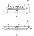
例如图22A的成膜装置100所示,这种气体供给喷嘴41在处理空间内突出地设置,在其表面上设有多个气体供给孔。这种气体供给喷嘴41作为非常小型的简单构成,能够在短时间内对其内部进行吹扫。并且,与气体喷头相比也非常易于制造。For example, as shown in the
但是,在使这种气体供给喷嘴41从处理容器2的顶板部突出的情况下,即使将晶片W尽可能地接近气体供给喷嘴41,也需要使顶板部最低以气体供给喷嘴41的突出高度远离晶片W。由此,可能导致处理环境气10的容积比较大,处理环境气10的吹扫耗费较多时间。并且当处理环境气10的容积较大时,为了保持在该处理环境气10中成膜所需的气体浓度,所需要的处理气体供给量也较多,因此会导致成膜成本的上升。However, in the case where such
为此,本发明者开发了如图22B所示的成膜装置101,将载置台3下方的空间从处理环境气10中区分开,通过将处理气体向侧方排出能够进一步减小吹扫所需的空间。但是,在这种装置的情况下,存在如下的问题:排出的处理气体的气流与处理容器2的侧壁部冲突而产生涡流,容易形成气体滞留而妨碍处理气体的完全排出。For this reason, the inventors of the present invention have developed a
JP特表2005-507030号公报(特别是0020段、0021段、图3)记载了一种在处理容器的顶板部设有锥面的ALD型的成膜装置。在该装置中,为了使基板表面的处理气体的供给速度均匀而设有锥面。并且处理气体经由在处理容器的顶部开口的气体流路向处理容器内供给。但是,该装置的构造基本上不同于使供给喷嘴从处理容器的顶板面突出的上述构造。Japanese Patent Publication No. 2005-507030 (particularly, paragraphs 0020 and 0021, FIG. 3 ) describes an ALD-type film forming apparatus in which a tapered surface is provided on the top plate of a processing container. In this apparatus, a tapered surface is provided in order to make the supply rate of the processing gas on the surface of the substrate uniform. Furthermore, the processing gas is supplied into the processing container through the gas channel opened at the top of the processing container. However, the configuration of this device is basically different from the above-mentioned configuration in which the supply nozzle protrudes from the top plate surface of the processing container.
发明内容 Contents of the invention
本发明针对上述问题提出了有效解决上述问题的方案。本发明目的在于提供构造简单易于制造的气体供给装置。并且,本发明的另一目的在于提供一种成膜装置以及成膜方法,例如在采用ALD等工艺的情况下能够发挥良好的气体置换性并且有助于提高生产量。Aiming at the above problems, the present invention proposes a solution to effectively solve the above problems. The object of the present invention is to provide a gas supply device which is simple in structure and easy to manufacture. In addition, another object of the present invention is to provide a film forming apparatus and a film forming method, which can exhibit good gas replacement performance and contribute to an increase in throughput when, for example, ALD or the like is used.
本发明的气体供给装置,与载置于处理容器内的载置台上的基板对置地配置,供给对上述基板进行处理的处理气体,其特征在于,包括:顶板部件,其在与上述载置台上的基板相对的位置,为了构成气体的扩散空间而具有形成为朝向上述载置台逐渐扩展的形状的凹部;从上述凹部的顶部向该凹部内突出,具有多个沿该凹部的周向的气体供给孔的气体供给喷嘴。The gas supply device of the present invention is disposed facing a substrate placed on a stage in a processing container, and supplies a processing gas for processing the substrate, and is characterized in that it includes a top plate member placed on the stage and The position facing the substrate has a concave portion formed in a shape gradually expanding toward the above-mentioned mounting table in order to constitute a gas diffusion space; protruding from the top of the above-mentioned concave portion into the concave portion, there are a plurality of gas supply along the circumferential direction of the concave portion Holes for gas supply nozzles.
根据本发明,使用小型而构造简单的气体供给喷嘴供给处理气体,与例如层叠多个板的构造的气体喷头相比,易于制造而能够降低制造成本。According to the present invention, the processing gas is supplied using a small gas supply nozzle with a simple structure, which is easier to manufacture and can reduce manufacturing cost compared to, for example, a gas shower head having a structure in which a plurality of plates are stacked.
并且,气体供给喷嘴从形成为向顶板部件的下方侧逐渐扩展的形状的凹部的顶部向该凹部内突出,并且该喷嘴的整体或者一部分被容纳在该凹部内,因此能够减小在其与载置台之间形成的气体的扩散空间。由此,与例如气体喷头型的气体供给装置相比,能够抑制处理气体的供给量和供给时间。并且,在需要吹扫工序的情况下,也能够抑制吹扫工序所需的时间。从而有利于变动成本的降低以及处理的生产量提高。In addition, since the gas supply nozzle protrudes into the recess from the top of the recess formed in a shape that gradually expands toward the lower side of the top plate member, and the whole or part of the nozzle is accommodated in the recess, it is possible to reduce the contact between the gas supply nozzle and the load. The gas diffusion space formed between the sets. Accordingly, compared with, for example, a gas shower head type gas supply device, the supply amount and supply time of the processing gas can be suppressed. Furthermore, when a purge step is required, the time required for the purge step can also be suppressed. This contributes to the reduction of variable costs and the improvement of processing throughput.
例如,上述凹部由朝向上述载置台逐渐扩展的锥面形成。For example, the concave portion is formed by a tapered surface gradually expanding toward the mounting table.
并且优选,上述气体供给喷嘴设置在贯通上述顶板部件的气体供给管的顶端部,上述气体供给喷嘴和上述气体供给管对于多种处理气体是通用的。In addition, it is preferable that the gas supply nozzle is provided at the tip end of a gas supply pipe penetrating the top plate member, and the gas supply nozzle and the gas supply pipe are common to various processing gases.
并且优选,上述气体供给管构成为相对于上述顶板部件可自由装卸。Moreover, it is preferable that the said gas supply pipe is comprised so that attachment and detachment are free with respect to the said top plate member.
并且优选,上述气体供给孔,相对于上述凹部的中心轴,具有至少10度的倾角地开口。Furthermore, it is preferable that the gas supply hole opens at an inclination angle of at least 10 degrees with respect to the central axis of the recessed portion.
并且优选,上述气体供给喷嘴,随着从顶端部侧向基端部侧接近,该气体供给喷嘴表面的单位面积上的气体供给孔的开口数增加。In addition, it is preferable that the number of openings of the gas supply holes per unit area of the surface of the gas supply nozzle increases as the gas supply nozzle approaches from the distal end side to the base end side.
另外,本发明成膜装置,对处理容器内的载置台上载置的基板供给彼此不同的多种处理气体并且使这些处理气体反应而在上述基板的表面形成薄膜,其特征在于,包括:具有载置基板的载置台的处理容器;具有上述特征之任一的气体供给装置。In addition, the film forming apparatus of the present invention supplies a plurality of processing gases different from each other to a substrate placed on a mounting table in a processing container and reacts these processing gases to form a thin film on the surface of the substrate, and is characterized in that it includes: A processing container for a mounting table on which a substrate is placed; a gas supply device having any one of the above characteristics.
该成膜装置,优选具有控制部,其交替进行作为第一处理气体供给原料气体而使基板吸附的阶段,以及作为第二处理气体供给与上述原料气体反应的反应气体而在基板上生成反应生成物的阶段,并且向装置各部输出控制信号,以使得在上述的两个阶段之间,进行利用吹扫气体吹扫处理环境气的阶段。This film forming apparatus preferably has a control unit that alternately performs a stage of supplying a raw material gas as a first processing gas to adsorb the substrate, and supplying a reactive gas that reacts with the raw material gas as a second processing gas to generate a reaction gas on the substrate. and output control signals to each part of the device, so that between the above two stages, a stage of purging the ambient gas with purge gas is performed.
并且优选,该成膜装置设有真空排气路,其与上述气体供给装置的上述扩散空间连通,将该扩散空间内的环境气从侧方排出。Furthermore, it is preferable that the film forming apparatus is provided with a vacuum exhaust path communicating with the diffusion space of the gas supply device, and exhausting the ambient gas in the diffusion space from the side.
并且优选,上述凹部的上述载置台侧的开口部构成为,该开口部的投影面覆盖上述载置台上所载置的基板的面积的30%以上的区域。Furthermore, it is preferable that the opening of the concave portion on the side of the mounting table is configured such that a projected plane of the opening covers an area of 30% or more of the area of the substrate mounted on the mounting table.
另外,本发明的成膜方法,对处理容器内的载置台上所载置的基板供给彼此不同的多种处理气体并且使这些处理气体反应,在上述基板的表面形成薄膜,其特征在于,包括:将基板载置于处理容器内的载置台上的载置工序;利用具有上述特征之任一的气体供给装置供给处理气体的处理气体供给工序。In addition, the film forming method of the present invention is characterized in that a plurality of processing gases different from each other are supplied to a substrate placed on a mounting table in a processing container, and these processing gases are reacted to form a thin film on the surface of the substrate, which includes : a mounting step of placing a substrate on a mounting table in a processing container; and a processing gas supplying step of supplying a processing gas by the gas supply device having any one of the above characteristics.
优选上述处理气体供给工序,交替进行作为第一处理气体供给原料气体而使基板吸附的阶段,以及作为第二处理气体供给与上述原料气体反应的反应气体而在基板上生成反应生成物的阶段,并且在上述两个阶段之间进行利用吹扫气体吹扫处理环境气的阶段。Preferably, in the process gas supplying step, a step of supplying a raw material gas as the first processing gas to adsorb the substrate, and a step of supplying a reaction gas that reacts with the raw material gas as the second processing gas to generate a reaction product on the substrate are alternately performed, And between the above two stages, a stage of purging the ambient gas with purge gas is carried out.
另外,该成膜方法优选,还具有将上述气体供给装置的上述扩散空间内的环境气从侧方真空排气的工序。In addition, it is preferable that the film forming method further includes a step of evacuating the ambient gas in the diffusion space of the gas supply device from the side.
附图说明 Description of drawings
图1为本发明一实施方式的成膜装置的纵剖面图。FIG. 1 is a longitudinal sectional view of a film forming apparatus according to an embodiment of the present invention.
图2为从下面侧看设置于上述成膜装置的气体供给装置的立体图。FIG. 2 is a perspective view of a gas supply device provided in the above-mentioned film forming apparatus viewed from the bottom side.
图3为图2的气体供给装置中的气体供给喷嘴的放大立体图。Fig. 3 is an enlarged perspective view of a gas supply nozzle in the gas supply device of Fig. 2 .
图4为图2的气体供给装置的纵剖面图。Fig. 4 is a longitudinal sectional view of the gas supply device of Fig. 2 .
图5为使图2的气体供给喷嘴与晶片对置的状态下的放大侧视图。5 is an enlarged side view of a state in which the gas supply nozzle of FIG. 2 is opposed to a wafer.
图6为上述成膜装置的气体供给路径图。FIG. 6 is a diagram showing a gas supply path of the above-mentioned film forming apparatus.
图7为上述成膜装置的第一作用图。Fig. 7 is a first action diagram of the above-mentioned film forming apparatus.
图8A、图8B为上述成膜装置的第二作用图。8A and 8B are the second action diagrams of the above-mentioned film forming apparatus.
图9为上述成膜装置进行的成膜处理的气体供给时序图。FIG. 9 is a gas supply timing chart for the film formation process performed by the above film formation apparatus.
图10为上述成膜装置的第三作用图。Fig. 10 is a third action diagram of the above-mentioned film forming apparatus.
图11A~图11D为上述气体供给装置的变形例。11A to 11D show modified examples of the above gas supply device.
图12A~图12G为上述气体供给喷嘴的变形例。12A to 12G show modified examples of the above gas supply nozzle.
图13为上述气体供给装置的第二变形例。Fig. 13 is a second modified example of the gas supply device.
图14为上述第二变形例的气体供给装置中的气体供给喷嘴的放大立体图。14 is an enlarged perspective view of a gas supply nozzle in the gas supply device according to the second modified example.
图15为从下面侧看第二实施方式的气体供给装置的立体图。Fig. 15 is a perspective view of the gas supply device according to the second embodiment seen from the lower side.
图16为图15的气体供给装置的纵剖立体图。Fig. 16 is a vertical perspective view of the gas supply device of Fig. 15 .
图17为图15的气体供给装置的纵剖面图。Fig. 17 is a longitudinal sectional view of the gas supply device of Fig. 15 .
图18为在实施例的模拟中使用的模型空间的立体图。Fig. 18 is a perspective view of a model space used in the simulation of the embodiment.
图19A、图19B为表示第一实施例的结果的说明图。19A and 19B are explanatory diagrams showing the results of the first example.
图20A~图20C为表示第二实施例的结果的说明图。20A to 20C are explanatory diagrams showing the results of the second example.
图21A~图21C为表示第三实施例的结果的说明图。21A to 21C are explanatory diagrams showing the results of the third example.
图22A、图22B为表示具有气体供给喷嘴的成膜装置的参考例的说明图。22A and 22B are explanatory views showing a reference example of a film forming apparatus having a gas supply nozzle.
具体实施方式 Detailed ways
以下参照图1至图6对本发明一实施方式的成膜装置1的构成进行说明。成膜装置1,作为第一处理气体使用含有锶(Sr)的原料气体(以下称为Sr原料气体),作为第二处理气体使用含有钛(Ti)的原料气体(以下称为Ti原料气体)。使这些处理气体与第三处理气体即作为氧化气体的臭氧气反应,从而利用ALD工艺在基板、例如是直径300mm的晶片表面上形成薄膜,该薄膜由高介电体材料即钛酸锶(SrTiO3,以下略记为STO)构成。Hereinafter, the configuration of a film forming apparatus 1 according to an embodiment of the present invention will be described with reference to FIGS. 1 to 6 . The film forming apparatus 1 uses a source gas containing strontium (Sr) (hereinafter referred to as Sr source gas) as a first process gas, and uses a source gas containing titanium (Ti) (hereinafter referred to as Ti source gas) as a second process gas. . These processing gases are reacted with the third processing gas, i.e., ozone gas as an oxidizing gas, thereby utilizing the ALD process to form a thin film on the surface of a substrate, such as a wafer with a diameter of 300 mm, which is made of high dielectric material, namely strontium titanate (SrTiO , hereinafter abbreviated as STO) constitutes.
如图1的纵剖面图所示,该成膜装置1具有形成真空容器的处理容器2、在该处理容器2内设置而用于载置作为基板的晶片W的载置台3、用于向与该载置台3对向地设置于处理容器2的上部的晶片W表面供给处理气体的气体供给装置4。As shown in the longitudinal sectional view of FIG. 1 , the film forming apparatus 1 has a
载置台3构成为包括支撑晶片W的相当于载置台主体的台体31和覆盖该台体31的台罩32。台体31以例如氮化铝或石英等为材料形成例如扁平的圆板状。在台体31内部埋设有台体加热器33,其对载置台3的载置面加热而使晶片W升温至成膜温度。该台体加热器33例如由片状的电阻发热体构成,从电源部68供电而能够将载置台3上载置的晶片W加热至例如280℃。并且,在台体31内设有未图示的静电卡盘,能够将载置于载置台3上的晶片W通过静电吸附而固定。The
另一方面,与台体31一起构成载置台3的台罩32,覆盖台体31的上表面和侧面,起到防止反应生成物或反应副产物等反应物向台体31表面堆积的效果。台罩32例如构成为石英制的可装卸的罩部件(被称为防附着护罩(デポシ一ルド)),在其上表面中央区域形成有圆形的凹部,该凹部具有比晶片W略大的直径。通过这种凹部能够定位在台罩32的载置面上载置的晶片W。On the other hand, the
载置台3通过柱状的支撑部件34支撑例如台体31的下表面侧中央部。该支撑部件34构成为能够通过升降机构69升降。通过升降支撑部件34,能够使载置台3在能够与外部的输送机构交接晶片W的交接位置以及能够处理晶片W的处理位置之间例如以最长80mm的程度升降。The mounting table 3 supports, for example, the center portion on the lower surface side of the
如图1所示,支撑部件34贯通处理容器2的底面部、具体为后述的下侧容器22的底面部,并且与通过升降机构69升降的升降板23连接。这里,升降板23与下侧容器22之间通过波纹管24气密地连接。As shown in FIG. 1 , the
另外,载置台3具有用于支撑晶片W的背面而使该晶片W相对于载置台3的载置面升降的例如3根升降销35。这里升降销35例如图1所示,在载置台3移动到晶片W的处理位置的状态下,各升降销35的扁平头部在台体31的上表面被卡定,并且其下端部从台体31的底面突出,从而以在上下方向贯通台体31的状态被安装。In addition, the
在上下方向贯通台体31的各升降销35的下方侧设有环状的升降部件36。在载置台3下降到晶片W的交接位置的状态下,通过使升降部件36升降而能够使各升降销35升降。由此,由各升降销35支撑着背面的晶片W,能够相对于载置台3的载置面升降。An
这里,在台罩32的上表面侧的、上述升降销35贯通的位置,设有开口部(扩径凹部),该开口部用于容纳升降销35的头部。由此,如图1所示在载置台3移动到晶片W的处理位置的状态下,台罩32的上表面与各升降销35的头部上表面基本处于同一平面,能够在载置台3的上表面形成平坦的晶片W载置面。并且,台罩32的侧壁部延伸到台体31的下方侧,形成从侧面包围台体31的下方区域的裙部321。Here, an opening (diameter-enlarged concave portion) for accommodating the head of the
接着对处理容器2的构成进行说明。处理容器2构成为在扁平的碗形的下侧容器22之上层叠有呈环状形成的排气管21。下侧容器22例如由铝等构成,在其底面上设有贯通孔221,被上述台体31的支撑部件34贯通。Next, the configuration of the
并且,在该贯通孔221周围的例如四个位置,设有吹扫气体供给路222。经由该吹扫气体供给路222,能够将从吹扫气体供给源66供给的氮气等吹扫气体送入下侧容器22内。In addition, purge
并且,图1中虚线所示输送口28是用于通过外部的输送机构进行晶片W的搬入搬出的开口部。该输送口28能够通过闸门阀开闭,上述闸门阀在处理容器2的侧壁部223上设置而没有图示。In addition, the
排气管21例如是铝制的,且构成为截面为方形的管材弯曲形成的环状体。该环状体的内径和外径构成为与下侧容器22的侧壁部223的内径和外径基本相同的尺寸。这里,将排气管21的靠近扩散空间40一侧的壁面称为内壁面,将远离扩散空间40的一侧壁面称为外壁面。在排气管21的内壁面的上端部,在周向上间隔地设有多个延伸于横向(周向)的缝隙状的真空排气口211。并且,在排气管21的外壁面的例如一个部位连接有排气管29。例如,采用与该排气管29连接的真空泵67,能够进行经由各真空排气口211的真空排气。并且如图1所示,在排气管21上以覆盖从其上表面侧到外壁面以及下表面侧的外周部的方式设置隔热部件212。The
这种排气管21经由隔热部件212在下侧容器22上层叠而以彼此隔热的状态形成一体而构成处理容器2。并且,在排气管21的内壁面上设置的多个真空排气口211,朝向包括在气体供给装置4与载置台3之间形成的扩散空间40的处理环境气开口。因此,能够经由这些真空排气口211对处理环境气进行真空排气。将该处理环境气向真空泵67引导的空间,相当于成膜装置1的真空排气路。
并且,在处理容器2内部如图1所示设有内部模块26,该内部模块26用于将下侧容器22内的空间即下部空间从包含处理环境气的位于载置台3上部的上部空间区分开。该内部模块26例如为铝制的环状部件,形成为能够装填下侧容器22的侧壁部223的内壁面与载置台3的侧周面(裙部321的侧周面)之间的空间的尺寸。Furthermore, as shown in FIG. 1 , an
在内部模块26的上表面外周部设有向更外侧扩展的突起缘262。通过在下侧容器22的侧壁部223和排气管21的内壁面侧的下端部之间插入的中间环体252上卡定上述突起缘262,从而内部模块26以从下侧容器22的内壁面环状突出的方式被固定在处理容器2内。On the outer peripheral portion of the upper surface of the
并且如图1所示,内部模块26的从上表面朝向内周面的区域,被石英制的块罩261覆盖。由此,能够抑制反应物向其表面堆积。具体而言,当载置台3位于处理位置时,块罩261经由例如2mm的间隙包围台罩32的侧面(裙部321的侧面)。由此,形成处理环境气难以向下部空间扩散的状态。Furthermore, as shown in FIG. 1 , the area from the upper surface toward the inner peripheral surface of the
并且,在排气管21的内壁面与后述的顶板部件42之间的环状空间内配设截面形成倒L字形的环部件即挡环27,其通过减小向该空间内的流导(conductance)而使来自该空间的真空排气的周向上的均匀性提高。In addition, in the annular space between the inner wall surface of the
接着,对气体供给装置4的构成进行说明。如图1所示,气体供给装置4具有顶板部件42和气体供给喷嘴41,上述顶板部件42用于在和载置台3之间形成气体的扩散空间40,上述气体供给喷嘴41向该扩散空间40供给处理气体或吹扫气体。Next, the configuration of the
如图2所示,顶板部件42例如为铝制的大致圆板部件,封闭处理容器2的上表面侧的开口部,构成气密的真空容器。如图1和图2所示,在顶板部件42的上缘部设置有凸缘部421。该凸缘部421经由具有与该凸缘部421嵌合的台阶的环状的支撑部件25,载置固定于排气管21的上表面侧。此时,顶板部件42的侧周面成为与上述支撑部件25以及上述挡环27的内周面密合的状态。并且,凸缘部421通过未图示的例如螺栓等,相对于支撑部件25可装卸地紧固。As shown in FIG. 2 , the
如图1和图4所示,在顶板部件42的下表面侧中央部,设有凹部422,该凹部422形成为朝向载置台3侧逐渐扩展的形状。如图2所示,凹部422与顶板部件42的底面同心圆状开口,该开口部,在与载置台3上的晶片W相对的状态下,以其投影面覆盖晶片W的面积的30%以上、例如72%的区域的方式开口。在本实施方式中,开口部的直径例如为255mm。并且,在凹部422与载置台3之间形成的空间,是用于将向处理容器2内供给的各种气体朝向晶片W表面扩散的扩散空间40。As shown in FIGS. 1 and 4 , a recessed
半球状的气体供给喷嘴41从凹部422的顶部朝向载置台3突出于凹部422内。在该气体供给喷嘴41上设有多个气体供给孔411。如图1、图3、图4所示,气体供给喷嘴41安装在气体供给管43的顶端部。气体供给管43,贯通顶板部件42的大致中央部,从而使气体供给喷嘴41向凹部422内突出。并且在气体供给管43下方侧的侧周部设有凸缘部432。该凸缘部432在顶板部件42的上表面通过例如螺栓等固定,气体供给管43相对于顶板部件42可自由装卸。The hemispherical
如图4所示,气体供给喷嘴41以及气体供给管43的内部为空洞。该空洞部用作气体的流通空间430。并且,在气体供给管43侧面的基端侧固定有总管431。由此,经由总管431→流通空间430→气体供给孔411这样的路径向扩散空间40内供给各种气体。具体而言,从总管431供给Sr原料气体、Ti原料气体以及臭氧气这3种处理气体,并且供给作为各种处理气体的载体气体以及吹扫气体利用的气体、例如氩气(Ar)。As shown in FIG. 4 , the insides of the
气体供给喷嘴41上设置的多个气体供给孔411,例如在从该半球状的气体供给喷嘴41的中心位置向径向延伸的直线上,沿着包围该气体供给喷嘴41的凹部422的周向排列并开口。The plurality of gas supply holes 411 provided in the
这里,ALD是通过重复使一层或者少数层的原子层或分子层在晶片W的表面上吸附并反应而形成薄膜的过程来逐渐层叠该薄膜,以形成均匀的膜的工艺。因此,如果原料气体到达晶片W表面时的气体走势过强,则会导致在该区域上吸附、附着预定量以上的气体,从而该区域的膜厚变厚的问题。为此,本实施方式的气体供给喷嘴41,如图4所示,不是在喷嘴41的顶端部设置气体供给孔411,而使仅在比顶端部靠近外侧的区域形成气体供给孔411。由此,各气体供给孔411相对于气体供给喷嘴41的中心轴所成角度“θ”至少为10°以上、例如25°以上。由此,原料气体到达晶片W表面时的走势减弱(具体的作用效果将在后面叙述)。Here, ALD is a process of gradually stacking thin films to form a uniform film by repeating the process of forming a thin film by adsorbing and reacting one or a small number of atomic layers or molecular layers on the surface of the wafer W. Therefore, if the gas movement when the source gas reaches the surface of the wafer W is too strong, more than a predetermined amount of gas will be adsorbed and adhered to this region, resulting in a problem that the film thickness of this region will become thicker. Therefore, the
并且如图3所示,气体供给喷嘴41将气体供给孔411配置为单位面积的开口数在气体供给喷嘴41的顶端侧区域较少,而越接近基端侧越多。其原因在于,如图5所示在对将气体供给喷嘴41顶端侧的圆形区域“S1”、具有与该区域相等面积的基端侧的圆形区域“S2”投射于晶片W表面所得投影面“P1、P2”的面积进行相互比较时,基端侧的圆形区域“S2”的投影面“P2”大于顶端侧的圆形区域“S1”的投影面“P1”的面积。即,气体供给孔411的开口面积在顶端侧和基端侧相同的情况下,这些投影面内的单位面积的气体供给孔411的开口数基本一致,以这种方式来调节各区域“S1、S2”内配置的气体供给孔数量。或者,在顶端侧与基端侧的气体供给孔411的开口面积不同的情况下,顶端侧的开口面积与基端侧的开口面积之比为P1∶P2。即,在顶端侧和基端侧具有与投影面积P1∶P2成比例的气体供给孔的开口面积,由此,能够使到达晶片W表面时的气体浓度在晶片W面内尽可能均匀。Furthermore, as shown in FIG. 3 , in the
在总管431上,如图6所示,连接有用于供给各种气体的气体供给管路610、620、630。这些气体供给管路610~630在上游侧分别与各种气体供给源61~64连接。
具体而言,Sr原料气体供给管路610与Sr原料供给源61连接。在该供给源61中贮存有例如Sr(THD)2(ストロンチウムビステトラメチルヘプタンジオナト:双(四甲基庚二酮根)合锶)或Sr(Me5Cp)2(ビスペンタメチルシクロペンタジエニエルストロンチウム:双(五甲基环戊二烯基)合锶)等液体Sr原料。如果将这些Sr原料向供给管路压送,则会通过汽化器611汽化而成为Sr原料气体,经由该气体的供给管路610向总管431供给。Specifically, the Sr raw material
并且,Ti原料气体供给管路620与Ti原料供给源62连接。在该供给源62中贮存有例如Ti(OiPr)2(THD)2(チタニウムビスイソプロポキサイドビステトラメチルヘプタンジオナト:双(异丙醇)双(四甲基庚二酮根)合钛)或Ti(OiPr)(チタニウムテトライソプロポキサイド:四(异丙醇)合钛)等液体Ti原料。与Sr原料的情况同样地,通过汽化器621汽化的Ti原料气体,经由该气体的供给管路620向总管431供给。Furthermore, the Ti raw material
并且,臭氧气供给管路630与例如通过周知的臭氧发生器等构成的臭氧气供给源63连接。Moreover, the ozone
Sr原料气体供给管路610、Ti原料气体供给管路620以及臭氧气供给管路630分别在路径途中分支,与由氩气瓶等构成的吹扫气体供给源64连接。由此,能够向各供给管路610~630供给氩气作为各原料气体的载体气体、或者、各处理气体的吹扫气体。The Sr source
在气体供给管路610~630和气体供给源61~64之间,介入设置由阀门以及流量计等构成的流量控制设备组65。由此,能够基于来自后述的控制部7的指示来控制各种气体的供给时机以及供给量。Between the
回到成膜装置1的装置构成的说明,在顶板部件42的上表面和排气管21的外壁面的下表面侧以及上表面侧等,如图1所示那样地设置由片状的电阻发热体等构成的加热器44、213。这些加热器,通过从电源部68供给的电力对顶板部件42和排气管21的整体进行加热,能够防止反应物向气体供给喷嘴41的下表面或排气管21的内表面附着。另外为了便于图示,在图1以外的图中省略了加热器44、213的记载。并且,除了上述的加热器44、213以外,用于防止反应物附着的加热器例如也埋设于内部模块26内,但是为了便于说明而省略了图示。Returning to the description of the device configuration of the film forming apparatus 1, on the upper surface of the
成膜装置1具有控制部7,该控制部7对上述气体供给源61~64的气体供给动作、载置台3的升降动作、真空泵67的处理容器2内的排气动作、台体加热器33以及各加热器44、213的加热动作等进行控制。控制部7例如由设有未图示的CPU和存储部的计算机构成。在该存储部中存储有组合了针对如下控制的步骤(命令)群的程序,即:通过成膜装置1对晶片W进行成膜处理所需的控制、例如来自气体供给源61~64的各种气体供给的供给中断时机或供给量调整的控制、调节处理容器2内的真空度的控制、载置台3的升降动作控制、各加热器33、44、213的温度控制等。这种程序通常存储在例如硬盘、光盘、磁光盘、存储卡等存储介质中,并且从此开始安装到存储部中。The film forming apparatus 1 has a
以下对采用上述气体供给装置4的成膜装置1的动作进行说明。The operation of the film forming apparatus 1 using the
首先如图7所示,输送口28敞开,外部的输送机构从输送口28进入,将晶片W搬入处理容器2内。接着,经由升降销35将晶片W载置于位于交接位置的载置台3上。通过未图示的静电卡盘将晶片W吸附固定于载置台3上。此时,通过加热器213等将排气管21和内部模块26的表面例如分别加热至230℃。并且,通过加热器44将处理容器2内的顶板部件42的表面加热至例如250℃。接着关闭输送口28,在处理容器2内成为气密状态之后,通过真空泵67经由排气管21将处理容器2内形成负压状态。First, as shown in FIG. 7 , the
此时如上所述,内部模块26固定在比晶片W的交接位置(设置输送口28的位置)高的位置。因此如图7所示,在使载置台3下降到晶片W的交接位置的状态下,下侧容器2内的空间成为与处理空间连通的(未区分开的)状态。因此,在真空排气工序中,包含下侧容器2内的处理容器2内整体被真空排气。At this time, as described above, the
当处理容器2内被真空排气达到所定压力时,继续保持真空排气状态,使载置有晶片W的载置台3,上升到根据规定了对晶片W的处理条件的方法选择的处理位置。在本实施方式的成膜装置1中,对于处理位置可以变更从晶片W的表面到顶板部件42的下表面的距离“h”(以下成为间隙)。具体而言,能够在从如图8A所示“h=40mm”的处理位置到如图8B所示“h=8mm”的处理位置之间在上下方向自由变化。在使载置台3上升到所定的处理位置后,例如图8A或图8B所示,台罩32的侧周面或者从该侧周面延伸的裙部321成为被内部模块26包围的状态,载置台3上方的上部空间和下侧容器22内的空间即下部空间,成为通过载置台3和内部模块26彼此区分开的状态。When the inside of the
如上所述那样,上部空间和下部空间被区分开之后,通过吹扫气体供给路222开始向下侧容器22内导入吹扫气体。并且,通过台体加热器33将晶片W的温度提升至例如280℃。然后,开始STO的成膜处理。另外,在图7、图8A、图8B各图中,为了便于图示而省略了台体加热器33的记载。并且下面以图8B所示位置说明晶片W的处理位置。After the upper space and the lower space are partitioned as described above, introduction of the purge gas into the
采用ALD工艺的STO的成膜处理,基于图9所示的气体供给时序来进行。图9的(a)~(d)所示的空白柱形图表示来自各气体供给源61~64的各种气体(Sr原料气体、Ti原料气体、臭氧气、吹扫气体)的供给量。The STO film formation process using the ALD process is performed based on the gas supply sequence shown in FIG. 9 . The blank bar graphs shown in (a) to (d) of FIG. 9 represent the supply amounts of various gases (Sr source gas, Ti source gas, ozone gas, purge gas) from the respective
并且,图10示意性地表示该时序执行中的处理容器2内的气体流动。In addition, FIG. 10 schematically shows the flow of gas in the
根据该气体供给时序,如图9的(a)所示,首先进行Sr原料气体的供给(Sr原料气体供给工序)。此时,Sr原料气体通过气体供给管43内的流通空间430而到达气体供给喷嘴41,通过气体供给孔411供给到扩散空间40内。气体供给喷嘴41流出的Sr原料气体如图10所示,在扩散空间49内放射状扩散而逐渐流向载置台3上的晶片W。According to this gas supply sequence, as shown in FIG. 9( a ), the supply of Sr source gas is performed first (Sr source gas supply step). At this time, the Sr source gas passes through the
此时如图1所示,在处理容器2中,设置于排气管21的真空排气口211以包围扩散空间40的方式配置。因此,到达晶片W的原料气体,朝向这些真空排气口211逐渐向晶片W的径向流动。由此,不与凹部422的开口部相对置的晶片W的周缘区域也能够在气体朝向真空排气口211流动时吸附原料气体。即,除了与凹部422相对置的晶片W的区域之外,该周缘区域也可以理解为晶片W的扩散空间40(处理环境气)。这样,通过原料气体在晶片W的径向上流动,与侧流方式相比缩短了原料气体的移动距离。由此,能够使各原料气体的分子在晶片W的径向上均匀地吸附。At this time, as shown in FIG. 1 , in the
这里,本实施方式的气体供给装置4,将气体供给喷嘴41容纳在凹部422内。由此,例如与作为背景技术说明的图18B所示成膜装置101相比,减小了扩散空间40(与凹部422相对置的空间以及晶片W的周缘区域上方的空间)的容积。其结果是,能够以更少的气体供给量使原料气体在晶片W的整个面上均匀地吸附,并且可以缩短原料气体的供给时间。Here, in the
另一方面,例如凹部422的开口部的面积过小时,不与该开口部相对置的晶片W的周缘区域的面积增大,即,晶片W和顶板部件42的底面中与水平部分之间的狭窄流路内在晶片W表面上吸附气体的面积的比例增大。当这样的面积的比例增大时,向晶片W的整个面供给气体所需的时间增加,并且在气体的流动中产生紊流,会导致供给到上述周缘区域内的气体浓度变得不均匀。On the other hand, for example, if the area of the opening of the
为了避免这种情况,在本实施方式的处理容器2中,凹部422的开口部构成为能够覆盖晶片W的面积的30%以上、例如70%左右的区域。由此,能够对晶片W的大部分区域从凹部422直接供给气体。由此,保证了短时间内的均匀的气体供给。凹部422的开口部也可以以覆盖晶片W的整体的方式开口。并且,当该开口部的面积增大时,扩散空间40的容积增大,也有缺点。即,会发生气体供给量的增大或者和气体供给时间的增加等情况。为了兼顾该缺点,应当适宜地确定开口部422的开口部尺寸和形状。In order to avoid this, in the
并且,如上所述,本实施方式的气体供给喷嘴41,在除去顶端部的区域(比顶端部靠外侧的区域)设有气体供给孔411。并且,气体供给孔411如图4所示,相对于气体供给喷嘴41的中心轴(凹部422的中心轴)的角度“θ”为10°以上、例如25°以上。采用这种构造,从流通空间430流下来的原料气体的流动方向受到气体供给喷嘴41的顶端部阻挡而变化。此时,压力损失增大,气体供给喷嘴41内的压力提高,因此从顶端侧的气体供给孔411朝向晶片W的原料气体的走势减弱,从基端侧的气体供给孔411朝向晶片W的原料气体的走势增强。由此,能够从气体供给喷嘴411的全部的气体供给孔411均匀地喷出气体。并且,由于气体供给孔411以角度“θ”(倾斜)开口,因此从沿着气体喷出方向的气体供给孔411到晶片W表面的距离增大。这一点也能够减弱到达晶片W表面时的原料气体的走势。通过上述的作用抑制过量的原料气体向晶片W表面吸附或者附着,特别是抑制气体供给喷嘴41正下方区域的膜厚增大的缺陷产生。Furthermore, as described above, the
并且,虽然没有在气体供给喷嘴41的顶端部设置气体供给孔411,但是在该顶端部正下方的晶片W的表面上,通过原料气体的扩散(特别是原料气体到达晶片W表面时的流动方向的变化)从周围供给原料气体,从而能够确认不会发生成膜方面的问题。In addition, although the
并且进一步采用图3和图5进行说明,在本实施方式的气体供给喷嘴41中,供给孔411的开口数量越是顶端侧区域越少而越是基端侧区域越多。由此,关于从气体供给喷嘴41朝向晶片W上的气体供给方向的投影面,单位面积上的气体供给孔411的配置数量基本均匀。由此,如图10示意性所示,供给到晶片W表面的单位面积的气体流线的条数基本相等。因此,能够使原料气体的供给浓度在晶片W面内更加均匀。3 and 5 , in the
这样,经过所定时间,在晶片W上形成Sr原料气体的吸附层后,停止Sr原料气体的供给,如图9(d)所示,从吹扫气体供给源64供给吹扫气体。由此,处理环境气、气体供给喷嘴41和气体供给管43内残留的Sr原料气体被吹扫(Sr原料气体吹扫工序)。导入气体供给管43的吹扫气体,经由与上述的Sr原料气体共同的路径,逐渐向真空排气口211流动。此时,如上所述,扩散空间40的容积比较小,并且与气体喷头相比,气体供给喷嘴41和气体供给管43的尺寸也减小,因此被吹扫的Sr原料气体的残留量减少,即能够减少昂贵的原料气体的消耗量,并且缩短该吹扫工序所需的时间。In this way, after a predetermined time elapses and an adsorption layer of the Sr source gas is formed on the wafer W, the supply of the Sr source gas is stopped, and the purge gas is supplied from the purge
在Sr原料气体的吹扫结束后,如图9(b)所示供给Ti原料气体(Ti原料气体供给工序)。Ti原料气体通过与Sr原料气体和吹扫气体共同的路径向扩散空间40内被供给。并且,在从相对于凹部422的开口部的区域流向周缘区域期间,该原料气体在晶片W表面上均匀吸附。After the purging of the Sr source gas is completed, the Ti source gas is supplied as shown in FIG. 9( b ) (Ti source gas supply step). The Ti source gas is supplied into the
经过所定时间,形成Ti原料气体的吸附层后,停止Ti原料气体的供给,按照与Sr原料气体的吹扫相同的顺序,进行残留的Ti原料气体的吹扫(图9(d),Ti原料气体吹扫工序)。After a predetermined period of time, after the adsorption layer of the Ti raw material gas is formed, the supply of the Ti raw material gas is stopped, and the residual Ti raw material gas is purged in the same order as that of the Sr raw material gas (Fig. 9(d), Ti raw material gas gas purging process).
接着,臭氧气通过与各原料气体和吹扫气体共同的路径被供给(图9(c),臭氧气供给工序)。在该工序中到达晶片W表面的臭氧,通过来自台罩32的热能与已经吸附于晶片W表面的原料气体反应而形成STO的分子层。Next, the ozone gas is supplied through a path common to each source gas and purge gas ( FIG. 9( c ), ozone gas supply step). The ozone that reaches the surface of the wafer W in this step reacts with the source gas adsorbed on the surface of the wafer W by heat energy from the
这样,在所定时间供给臭氧气后,停止臭氧气的供给,按照与上述各吹扫工序相同的顺序,吹扫臭氧气(图9(d),臭氧气吹扫工序)。In this way, after the ozone gas is supplied for a predetermined time, the supply of the ozone gas is stopped, and the ozone gas is purged in the same order as the above-mentioned purging steps ( FIG. 9( d ), ozone gas purging step).
虽然为了避免重复说明而在各工序的说明中没有提及,但是在Ti原料气体供给工序以及臭氧气供给工序中,也与Sr原料气体供给工序同样地,在向晶片W表面供给各处理气体时,能够以较少的供给量在短时间内在面内均匀地执行处理气体的供给。并且,各吹扫工序时吹扫的处理气体的残留量也较少,能够在短时间内结束吹扫。Although it is not mentioned in the description of each step to avoid duplication of description, in the Ti source gas supply step and the ozone gas supply step, as in the Sr source gas supply step, each process gas is supplied to the surface of the wafer W. , it is possible to uniformly supply the processing gas within a plane in a short time with a small supply amount. In addition, the residual amount of the process gas to be purged in each purge step is also small, and the purge can be completed in a short time.
并且如图9所示,将以上说明的六个工序作为一个循环,按照预先确定的次数例如100次重复进行该循环,从而使STO的分子层多层化。由此,能够形成具有所定膜厚的STO膜。在所需的成膜结束后,停止各种气体供给,载置晶片W的载置台3下降至输送口28,处理容器2内的压力恢复真空排气前的状态。其后,按照与搬入时相反的路径利用外部的输送机构搬出晶片W。由此结束一系列成膜动作。And as shown in FIG. 9 , the six steps described above are regarded as one cycle, and this cycle is repeated a predetermined number of times, for example, 100 times, so that the molecular layers of STO are multilayered. Thereby, an STO film having a predetermined film thickness can be formed. After the desired film formation is completed, the supply of various gases is stopped, the
根据本实施方式的气体供给装置4,具有以下效果。即,该气体供给装置4使用小型而构造简单的气体供给喷嘴41供给处理气体,因此与例如层叠多个板的构造的气体喷头等相比易于制造,从而有助于气体供给装置4以及成膜装置1的制造成本降低。According to the
并且,该气体供给喷嘴41从在顶板部件42的下方侧形成逐渐扩展的形状的凹部422的顶部突出设置,并且在该凹部422内容纳例如该喷嘴41的整体,因此能够减小在与载置台3之间形成的扩散空间40的容积。由此,例如与气体喷头型的气体供给装置相比,抑制了处理气体的供给量和供给时间。并且,也能够抑制吹扫工序所需的时间。因此,有助于减低波动成本以及处理的生产量提高。In addition, the
这里,设置于气体供给装置4的凹部422的形状,不限于上述实施方式中例示的锥面的情况。例如图11A或图11B所示,凹部422的截面形状可以由曲线规定。并且如图11C所示,凹部422的截面形状可以为台阶状。Here, the shape of the
并且,如图11D所示,也可以不在凹部422内容纳气体供给喷嘴41的整体,而是例如该顶端部从凹部422突出。如果气体供给喷嘴41的一部分容纳在凹部422内,则与图18B所示情况相比,处理环境气的容积减小了,能够取得降低处理气体的供给量以及缩短吹扫时间等效果。In addition, as shown in FIG. 11D , instead of housing the entire
并且,气体供给喷嘴41和/或气体供给孔411的形状,也不限于上述实施方式中例示的形态。例如图12A所示,也可以采用水平方向的截面形状为多边形的气体供给喷嘴41a。Moreover, the shape of the
并且如图12B所示,可以采用从侧方看的形状为长方形(例如整体形状为圆柱或立方体)的气体供给喷嘴41b,或者如图12C、图12D、图12E所示,采用从侧方看的形状为大致圆锥形状的气体供给喷嘴41c、41d、41e。And as shown in Figure 12B, can adopt the
并且如图12F所示,也可以设置缝隙状穿设的气体供给孔411a,或者设置开口径根据位置变化的气体供给孔411b。Furthermore, as shown in FIG. 12F , a
并且如图12G所示,可以相对于气体供给喷嘴41g的壁面的法线方向倾斜地设置气体供给孔411c,使处理气体形成涡旋进行供给。此外,也可以设置锥状的气体供给孔411d,气体从各供给孔边扩散边供给。Furthermore, as shown in FIG. 12G , the
以上各种凹部422的形状以及气体供给喷嘴41、41a~41g的形态,例如根据处理气体的种类或工艺条件适当选择而装入气体供给装置4。The shapes of the above
采用图1进行说明,顶板部件42构成为相对于处理容器2可装卸。并且如图4所示,气体供给管43也相对于顶板部件42可装卸。因此,例如在处理气体的种类或工艺条件变化而需要将凹部422或气体供给喷嘴41变更为适于新工艺的情况时,可以仅更换需要变更的部分。由此,能够降低气体供给装置4的改造成本。Referring to FIG. 1 , the
特别如图4所示,气体供给喷嘴41比顶板部件42小型,能够与气体供给管43一起简单地装卸。因此,即使在对例如附着于内部的粉尘等进行定期清扫的情况下,也不必取下整个顶板部件42开放处理容器2而具有良好的维护性。并且,通过在气体供给喷嘴41和气体供给管43上形成螺纹而使他们彼此螺合等方法,可将气体供给喷嘴41从气体供给管43自由装卸地构成,从而能够进一步提高维护性。并且,例如气体供给装置4,如图13、图14所示,可以将气体供给喷嘴41h和气体供给管43a作为独立部件制造。此时,例如经由在顶板部件42上穿设的流通空间430a,能够将气体供给喷嘴41h和气体供给管43a连接。此时,气体供给喷嘴41h,例如经由其基端部设置的凸缘部412,可通过螺栓413等被固定在顶板部件42的底面上。In particular, as shown in FIG. 4 , the
并且,当然也可以根据需要采用在顶板部件42上固定的类型的气体供给喷嘴41。In addition, of course, the
接着参照图15至图17对第二实施方式的气体供给装置4a进行说明。在图15至图17的各图中,对于具有与图1至图10等所示第一实施方式的气体供给装置4相同的功能的构成要素,标记与第一实施方式的气体供给装置4相同的符号。Next, a
第二实施方式的气体供给装置4a,如图15至图17所示,气体供给喷嘴41i的喷嘴主体的形状为扁平的圆板形状,这与气体供给喷嘴41为半球形的第一实施方式的气体供给装置4不同。In the
具体而言,在第二实施方式的气体供给装置4a中,例如直径D形成为100mm而高度h’为10mm的圆板形状的气体供给喷嘴41i,从在顶板42的下面侧设置的凹部422的顶部向载置台3侧突出。并且,在该圆板形状的气体供给喷嘴41i的底面以及侧面上,设有多个气体供给孔411,来自气体供给管43的处理气体,如图17所示,经由这些气体供给孔411向扩散空间40内供给。Specifically, in the
通过这样使气体供给喷嘴41i成为扁平形状,即使减小例如处理空间40的容积,也易于在凹部422内容纳气体供给喷嘴41i的整体,能够减少处理气体的供给并且缩短吹扫时间。具体而言,例如图11D所示的气体供给装置4那样,处理空间40的容积减小的结果是,与半球形状的气体供给喷嘴41从凹部422突出的状态的供给装置4相比,能够减小如图17所示从凹部422的顶部到气体供给喷嘴41i的底面的高度(图中标记为“h’”)与从气体供给喷嘴41i的底面到晶片W的距离(图中标记为“h”)的合计“h’+h”,从而进一步减小处理空间40的容积。并且如图11D所示,在气体供给喷嘴41从凹部422突出的情况下,间隙调整为,以气体供给喷嘴41的下端为基准,到晶片W表面的距离为预先设定的范围内的值。By making the gas supply nozzle 41i flat in this way, even if the volume of the
并且,通过使气体供给喷嘴41i为扁平形状,能够抑制气体供给喷嘴41i内的空间的容积增大,并且能够增大该喷嘴41i的外表面积。其结果是,例如与气体喷头相比,气体供给喷嘴41i和气体供给管43的尺寸减小,从而内部的气体置换变得容易。另一方面,与半球形状的气体供给喷嘴41相比,能够从更开阔的面朝向晶片W供给处理气体。特别在本实施方式的气体供给喷嘴41i中,不仅在底面而且也在侧面上形成气体供给孔411,因此处理气体的供给面进一步增大,能够沿着凹部422的逐渐扩展的面,使处理气体在更宽的区域上扩散。换言之,形成为扁平形状的气体供给喷嘴41i,兼具内部容积较小的喷嘴的优点以及处理气体的供给面较宽的气体喷头的优点,从而能够在更短时间内执行处理气体的供给乃至吹扫。Furthermore, by forming the gas supply nozzle 41i into a flat shape, it is possible to suppress an increase in the volume of the space in the gas supply nozzle 41i and to increase the outer surface area of the nozzle 41i. As a result, the size of the gas supply nozzle 41i and the
并且如图17所示,该多个气体供给孔411与第一实施方式的气体供给喷嘴41同样地,不是设置在气体供给喷嘴41i的底面中心部上,而是仅在外侧的区域上设置。由此构成为,各气体供给孔411相对于贯通圆板的底面中心的中心轴所成角度“θ”,至少为10°以上的例如35°以上。采用该构成,在气体供给喷嘴41i的底面中心区域(位于气体供给管43的正下方)中,处理气体的流动被阻挡而使从气体供给孔411喷出的处理气体的走势减弱,另一方面,在气体供给喷嘴41i的周缘区域上,作为处理气体的流动在上述中心区域被阻挡的结果,该喷嘴41i内部的压力提高,因此从气体供给孔411喷出的处理气体的走势增强。其结果是,能够从全部的气体供给孔411均匀地使处理气体喷出。And as shown in FIG. 17 , the plurality of gas supply holes 411 are not provided in the center portion of the bottom surface of the gas supply nozzle 41 i , but are provided only in the outer region, similarly to the
并且,这些气体供给孔411与第一实施方式的气体供给喷嘴41同样地配置为,越是气体供给喷嘴41i的顶端侧(在本例中为喷嘴41i的底面的中央区域侧),单位面积的开口数越少,越朝向基端侧(在本例中为从喷嘴41i的底面的周缘朝向侧面的区域侧)越增加。由此,如采用图5进行说明的那样,能够使处理气体到达晶片W表面时的处理气体的浓度,在晶片W的面内尽量均匀。这里,在各气体供给孔411的开口面积可以不同的情况下,可以在顶端侧和基端侧使该开口面积的比与图5所示投影面积的比P1/P2一致。这也与第一实施方式的供给喷嘴41相同。In addition, these gas supply holes 411 are arranged in the same manner as the
并且,形成为扁平形状的气体供给喷嘴41i,不限于图15所示从底面侧看的平面形状为圆形的圆板形状。例如气体供给喷嘴41i的平面形状可以为多边形或椭圆形等。Furthermore, the gas supply nozzle 41i formed in a flat shape is not limited to a disk shape in which the planar shape viewed from the bottom surface side is circular as shown in FIG. 15 . For example, the planar shape of the gas supply nozzle 41i may be a polygon, an ellipse, or the like.
此外,气体供给孔411不限于在扁平的气体供给喷嘴41i的底面以及侧面双方上设置的情况,例如仅在喷嘴主体底面设置气体供给孔411的情况也包含于本发明的技术范围。此时,通过使底面上设置的气体供给孔411的顶端部从喷嘴主体的底面略微突出,使气体朝向逐渐扩展形状的凹部422的底部喷出等,也能够与在喷嘴主体的侧面设置气体供给孔411的情况大致同样地供给气体。In addition, the
在上述的成膜装置1中,对将Sr原料和Ti原料以及臭氧气作为处理气体形成STO的薄膜的情况进行了说明,但是可以通过该成膜装置1成膜的薄膜种类不限于此。例如,可以将TEMAZ和臭氧气或者水蒸气作为处理气体,适用于形成氧化锆薄膜的工艺等。并且,可适用于该成膜装置1的工艺种类也不限于ALD或MLD,而可以是连续供给原料气体和反应气体的通常类型的CVD工艺。In the above-mentioned film forming apparatus 1, the case where the STO thin film is formed using the Sr raw material, the Ti raw material, and ozone gas as the processing gas has been described, but the types of thin films that can be formed by the film forming apparatus 1 are not limited thereto. For example, TEMAZ and ozone gas or water vapor can be used as a processing gas, which is suitable for the process of forming a zirconia thin film, etc. Also, the type of process applicable to the film forming apparatus 1 is not limited to ALD or MLD, but may be a general type of CVD process in which source gas and reaction gas are continuously supplied.
并且,虽然在上述实施方式中,作为被处理体以半导体晶片为例进行了说明,但是不限于此,也可以将本发明适用于玻璃基板、LCD基板、陶瓷基板等。In addition, in the above-mentioned embodiments, a semiconductor wafer has been described as an example of an object to be processed, but the invention is not limited thereto, and the present invention can also be applied to glass substrates, LCD substrates, ceramic substrates, and the like.
<实施例><Example>
(模拟1)(simulation 1)
生成第一实施方式的气体供给装置4的模型,模拟了处理气体供给时和吹扫气体供给时的处理环境气内的处理气体浓度分布。A model of the
A.模拟条件A. Simulation conditions
以将上述Sr原料、Ti原料的溶媒即甲苯在载体气体即氩气中挥发而形成的气体为处理气体的模型气体。使处理环境气内的温度为230℃,处理环境气出口的压力为45Pa。The model gas of the process gas is a gas obtained by volatilizing toluene, which is the solvent of the above-mentioned Sr raw material and Ti raw material, in argon gas, which is a carrier gas. The temperature inside the treated ambient air was set at 230° C., and the pressure at the outlet of the treated ambient air was set at 45 Pa.
(实施例1-1)(Example 1-1)
如图18所示,在上述实施方式的成膜装置1中,将气体流通的空间(流通空间430、气体供给喷嘴41内部以及扩散空间40(处理环境气)),以该空间的中央位置为基准生成在周向上分成四份的模型空间。并且,进行供给处理气体而使该模型空间内的处理气体的浓度从0vol%上升至4.0vol%的模拟。As shown in FIG. 18 , in the film forming apparatus 1 of the above-mentioned embodiment, the space through which the gas flows (the
此时,求出在从处理气体的供给开始经过0.01秒后的时刻的处理气体浓度分布。在供给处理气体时,为了防止该气体的逆扩散,与处理气体同时供给反向气体。在图18中,从实线箭头所示位置供给处理气体,从虚线箭头所示位置供给反向填充气体。At this time, the concentration distribution of the processing gas at the time of 0.01 second after the start of the supply of the processing gas was obtained. When the processing gas is supplied, in order to prevent back diffusion of the gas, a reverse gas is supplied simultaneously with the processing gas. In FIG. 18 , the processing gas is supplied from the position indicated by the solid line arrow, and the back filling gas is supplied from the position indicated by the dotted line arrow.
处理气体供给量Process gas supply
甲苯0.1g/minToluene 0.1g/min
氩气500mL/min(sccm)Argon 500mL/min(sccm)
反向填充气体供给量Reverse fill gas supply
氩气1000mL/min(sccm)Argon 1000mL/min(sccm)
(实施例1-2)(Example 1-2)
以与(实施例1-1)相同的条件,求出在从处理气体的供给开始经过0.1秒后的时刻的处理气体的浓度分布。Under the same conditions as in (Example 1-1), the concentration distribution of the processing gas at the time of 0.1 second after the start of supply of the processing gas was obtained.
(实施例2-1)(Example 2-1)
进行在以(实施例1-1)和(实施例1-2)的条件供给处理气体后的模型空间内,供给吹扫气体,使处理气体的浓度从4.0vol%降低至0vol%的模拟。A simulation was performed in which a purge gas was supplied to reduce the concentration of the processing gas from 4.0 vol% to 0 vol% in the phantom space after the processing gas was supplied under the conditions of (Example 1-1) and (Example 1-2).
求出在从处理气体的供给开始经过0.01秒后的时刻的处理气体浓度分布。图18的实线(以下称为处理气体管路)、虚线(以下称为反向填充气体管路)均供给作为吹扫气体的氩气。The processing gas concentration distribution at the time of 0.01 second elapsed from the start of the supply of the processing gas was obtained. Both the solid line (hereinafter referred to as process gas line) and the dotted line (hereinafter referred to as reverse filling gas line) in FIG. 18 are supplied with argon gas as a purge gas.
处理气体管路供给量Process gas pipeline supply
氩气500mL/min(sccm)Argon 500mL/min(sccm)
反向填充气体管路供给量Reverse fill gas line supply
氩气1500mL/min(sccm)Argon 1500mL/min(sccm)
(实施例2-2)(Example 2-2)
以与(实施例2-1)相同的条件,求出在从处理气体的供给开始经过0.1秒后的时刻的处理气体的浓度分布。Under the same conditions as in (Example 2-1), the concentration distribution of the processing gas at the time of 0.1 second after the start of supply of the processing gas was obtained.
(实施例2-3)(Example 2-3)
以与(实施例2-1)相同的条件,求出在从处理气体的供给开始经过0.5秒后的时刻的处理气体的浓度分布。Under the same conditions as in (Example 2-1), the concentration distribution of the processing gas at the time of 0.5 seconds after the start of the supply of the processing gas was obtained.
B.模拟结果B. Simulation Results
图19A和图19B表示(实施例1-1)~(实施例1-2)的模拟结果,图20A至图20C表示(实施例2-1)~(实施例2-3)的模拟结果。19A and 19B show the simulation results of (Example 1-1) to (Example 1-2), and FIGS. 20A to 20C show the simulation results of (Example 2-1) to (Example 2-3).
在这些图中,对于图18所示模型空间的底面(相当于晶片W的表面),用等浓度线区分表示处理气体的面内浓度分布。各图所示数值表示该区分开的区域内的气体浓度[vol%]的范围。In these figures, the in-plane concentration distribution of the process gas is shown by isoconcentration lines for the bottom surface of the model space shown in FIG. 18 (corresponding to the surface of the wafer W). The numerical value shown in each figure shows the range of the gas concentration [vol%] in the area|region divided by this area.
实际的模拟结果,通过计算机制图在分级表示浓度分布的彩色画面上输出,但是为了便于图示而在上述各图中表示概略的浓度分布。即,这些图中存在邻接的区划区域之间的浓度范围不连续的部位,表明实际浓度分布存在跳变,并且这些区域之间存在陡峭的浓度梯度。The actual simulation results are output by computer graphics on a color screen showing the density distribution in stages, but for the convenience of illustration, a rough density distribution is shown in each of the above-mentioned figures. That is, in these figures, there are discontinuous parts in the concentration range between adjacent compartmentalized areas, indicating that there is a jump in the actual concentration distribution, and there is a steep concentration gradient between these areas.
如图19A和图19B所示,根据(实施例1-1)~(实施例1-2)的结果,在处理气体导入开始后0.01秒,晶片W表面的大致一半的区域上升至3.5vol%~4.0vol%。并且,在处理气体导入开始后0.1秒,晶片W表面的大部分区域上升至4.0vol%的目标浓度。即,确认了能够在短时间内供给均匀的处理气体,并且具有充分的实用性。As shown in FIG. 19A and FIG. 19B, according to the results of (Example 1-1) to (Example 1-2), after 0.01 second after the start of the process gas introduction, the area of approximately half of the surface of the wafer W increased to 3.5 vol%. ~4.0vol%. Then, 0.1 second after the process gas introduction started, most of the surface of the wafer W rose to the target concentration of 4.0 vol%. That is, it was confirmed that a uniform processing gas can be supplied in a short time, and that it has sufficient practicality.
并且如图20A、图20B、图20C所示,根据(实施例2-1)~(实施例2-3)的结果,在吹扫气体供给开始后0.1秒的时刻,晶片W表面的气体浓度降低为大致接近0%(4.0×10⁻⁵vol%~8.0×10⁻⁵vol%)(图20B、实施例2-2),确认了能够在短时间基本完全吹扫干净。20A, 20B, and 20C, based on the results of (Example 2-1) to (Example 2-3), the gas concentration on the surface of the wafer W at 0.1 seconds after the start of the purge gas supply The reduction was approximately close to 0% (4.0×10 -5 vol% to 8.0×10 -5 vol%) ( FIG. 20B , Example 2-2 ), and it was confirmed that almost complete purge was possible in a short time.
根据以上结果,可以认为上述实施方式的处理容器2能够在短时间内均匀地供给、吹扫处理气体。From the above results, it can be considered that the
(模拟2)(simulation 2)
生成第二实施方式的气体供给装置4a的模型,模拟了处理气体供给时的处理环境气内的处理气体浓度分布,并与第一实施方式的气体供给装置4模型的模拟结果进行了比较。A model of the
A.模拟条件A. Simulation conditions
模型气体、处理环境气的温度和压力与(模拟1)相同。The temperature and pressure of the model gas, process ambient gas are the same as (Simulation 1).
(实施例3-1)(Example 3-1)
基于与图18相同的考虑,生成图15至图17所示第二实施方式的气体供给装置4a的模型空间,进行使处理气体的浓度从0.0vol%上升至4.0vol%的模拟。此时,求出在从处理气体的供给开始经过0.007秒后的时刻的处理气体的浓度分布。处理气体的供给量、反向填充气体的供给量等条件与(实施例1-1)相同。Based on the same considerations as in FIG. 18 , the model space of the
(实施例3-2)(Example 3-2)
以与(实施例3-1)相同的条件,求出在从处理气体的供给开始经过0.01秒后的时刻的处理气体的浓度分布。Under the same conditions as in (Example 3-1), the concentration distribution of the processing gas at the time of 0.01 second after the start of supply of the processing gas was obtained.
(实施例3-3)(Example 3-3)
以与(实施例3-1)相同的条件,求出在从处理气体的供给开始经过0.02秒后的时刻的处理气体的浓度分布。Under the same conditions as in (Example 3-1), the concentration distribution of the processing gas at the time of 0.02 seconds after the start of supply of the processing gas was obtained.
B.模拟结果B. Simulation Results
图21A至图21C表示(实施例3-1)~(实施例3-3)的模拟结果。在这些图中,与上述的图19A~图20C同样地,用等浓度线区划表示模型空间的底面(晶片W的表面)上的处理气体的面内浓度分布。为了避免图面显示变得繁杂,在图21A和图21B中省略了部分浓度范围的显示。21A to 21C show simulation results of (Example 3-1) to (Example 3-3). In these figures, the in-plane concentration distribution of the process gas on the bottom surface of the model space (the surface of the wafer W) is shown by isoconcentration line divisions as in the above-mentioned FIGS. 19A to 20C . In order to avoid complicated display of the drawings, the display of some concentration ranges is omitted in FIG. 21A and FIG. 21B .
如图21A至图21C所示,根据(实施例3-1)~(实施例3-3)的结果,在处理气体的导入开始后仅0.007秒,出现1.5vol%~2.0vol%的区域,在处理气体的导入开始后0.01秒,该区域的浓度上升至2.5vol%~3.0vol%。并且,在处理气体的导入开始后0.02秒,全体的大致1/3的区域的浓度上升至作为目标的4.0vol%,在该阶段几乎没有1.0vol%以下的浓度区域。并且确认了在处理气体导入开始后0.1秒,晶片W表面的大部分区域上升至4.0vol%的目标浓度(未图示)。根据这些结果,第二实施方式的气体供给装置4a,与第一实施方式的情况同样地,具有充分的实用性。As shown in FIG. 21A to FIG. 21C, according to the results of (Example 3-1) to (Example 3-3), only 0.007 seconds after the introduction of the processing gas, a region of 1.5 vol% to 2.0 vol% appeared, The concentration in this region rises to 2.5 vol% to 3.0 vol% 0.01 second after the start of introduction of the process gas. Then, 0.02 seconds after the start of the introduction of the processing gas, the concentration in approximately 1/3 of the entire region rises to the target 4.0 vol%, and there is almost no concentration region below 1.0 vol% at this stage. It was also confirmed that the target concentration of 4.0 vol% was raised to the target concentration of 4.0 vol% in most regions of the surface of the wafer W 0.1 second after the introduction of the process gas was started (not shown). From these results, the
Claims (13)
Applications Claiming Priority (3)
| Application Number | Priority Date | Filing Date | Title |
|---|---|---|---|
| JP2008039289 | 2008-02-20 | ||
| JP2008-039289 | 2008-02-20 | ||
| PCT/JP2009/053022 WO2009104732A1 (en) | 2008-02-20 | 2009-02-20 | Gas supply device |
Publications (2)
| Publication Number | Publication Date |
|---|---|
| CN101772833A CN101772833A (en) | 2010-07-07 |
| CN101772833B true CN101772833B (en) | 2012-04-18 |
Family
ID=40985609
Family Applications (1)
| Application Number | Title | Priority Date | Filing Date |
|---|---|---|---|
| CN2009801000561A Active CN101772833B (en) | 2008-02-20 | 2009-02-20 | gas supply device |
Country Status (6)
| Country | Link |
|---|---|
| US (1) | US8945306B2 (en) |
| JP (1) | JP5233734B2 (en) |
| KR (1) | KR101204614B1 (en) |
| CN (1) | CN101772833B (en) |
| TW (1) | TWI498988B (en) |
| WO (1) | WO2009104732A1 (en) |
Families Citing this family (434)
| Publication number | Priority date | Publication date | Assignee | Title |
|---|---|---|---|---|
| CN101772833B (en) * | 2008-02-20 | 2012-04-18 | 东京毅力科创株式会社 | gas supply device |
| US8110068B2 (en) * | 2008-03-20 | 2012-02-07 | Novellus Systems, Inc. | Gas flow distribution receptacles, plasma generator systems, and methods for performing plasma stripping processes |
| US9591738B2 (en) | 2008-04-03 | 2017-03-07 | Novellus Systems, Inc. | Plasma generator systems and methods of forming plasma |
| JP5304061B2 (en) * | 2008-07-09 | 2013-10-02 | 東京エレクトロン株式会社 | Plasma processing equipment |
| US10378106B2 (en) | 2008-11-14 | 2019-08-13 | Asm Ip Holding B.V. | Method of forming insulation film by modified PEALD |
| US9394608B2 (en) | 2009-04-06 | 2016-07-19 | Asm America, Inc. | Semiconductor processing reactor and components thereof |
| US8802201B2 (en) | 2009-08-14 | 2014-08-12 | Asm America, Inc. | Systems and methods for thin-film deposition of metal oxides using excited nitrogen-oxygen species |
| US20110120375A1 (en) * | 2009-11-23 | 2011-05-26 | Jusung Engineering Co., Ltd. | Apparatus for processing substrate |
| JP5927619B2 (en) * | 2010-05-06 | 2016-06-01 | エヴァテック・アクチェンゲゼルシャフトEvatec Ag | Plasma reactor |
| JP5572515B2 (en) * | 2010-10-15 | 2014-08-13 | 東京エレクトロン株式会社 | Film forming apparatus and film forming method |
| US10658161B2 (en) * | 2010-10-15 | 2020-05-19 | Applied Materials, Inc. | Method and apparatus for reducing particle defects in plasma etch chambers |
| US9312155B2 (en) | 2011-06-06 | 2016-04-12 | Asm Japan K.K. | High-throughput semiconductor-processing apparatus equipped with multiple dual-chamber modules |
| US10364496B2 (en) | 2011-06-27 | 2019-07-30 | Asm Ip Holding B.V. | Dual section module having shared and unshared mass flow controllers |
| US10854498B2 (en) | 2011-07-15 | 2020-12-01 | Asm Ip Holding B.V. | Wafer-supporting device and method for producing same |
| US20130023129A1 (en) | 2011-07-20 | 2013-01-24 | Asm America, Inc. | Pressure transmitter for a semiconductor processing environment |
| US9574268B1 (en) | 2011-10-28 | 2017-02-21 | Asm America, Inc. | Pulsed valve manifold for atomic layer deposition |
| US9017481B1 (en) | 2011-10-28 | 2015-04-28 | Asm America, Inc. | Process feed management for semiconductor substrate processing |
| US20130133701A1 (en) * | 2011-11-28 | 2013-05-30 | Intermolecular, Inc. | Method and apparatus for dispensing an inert gas |
| US9388492B2 (en) | 2011-12-27 | 2016-07-12 | Asm America, Inc. | Vapor flow control apparatus for atomic layer deposition |
| JP5788349B2 (en) * | 2012-03-19 | 2015-09-30 | 東京エレクトロン株式会社 | Plating processing apparatus, plating processing method, and storage medium |
| JP5929429B2 (en) * | 2012-03-30 | 2016-06-08 | 東京エレクトロン株式会社 | Deposition equipment |
| US9659799B2 (en) | 2012-08-28 | 2017-05-23 | Asm Ip Holding B.V. | Systems and methods for dynamic semiconductor process scheduling |
| US9021985B2 (en) | 2012-09-12 | 2015-05-05 | Asm Ip Holdings B.V. | Process gas management for an inductively-coupled plasma deposition reactor |
| JP6123208B2 (en) * | 2012-09-28 | 2017-05-10 | 東京エレクトロン株式会社 | Deposition equipment |
| US10714315B2 (en) | 2012-10-12 | 2020-07-14 | Asm Ip Holdings B.V. | Semiconductor reaction chamber showerhead |
| JP6196078B2 (en) * | 2012-10-18 | 2017-09-13 | 株式会社アルバック | Deposition equipment |
| US20160376700A1 (en) | 2013-02-01 | 2016-12-29 | Asm Ip Holding B.V. | System for treatment of deposition reactor |
| US9536710B2 (en) * | 2013-02-25 | 2017-01-03 | Applied Materials, Inc. | Tunable gas delivery assembly with internal diffuser and angular injection |
| US9484191B2 (en) | 2013-03-08 | 2016-11-01 | Asm Ip Holding B.V. | Pulsed remote plasma method and system |
| US9589770B2 (en) | 2013-03-08 | 2017-03-07 | Asm Ip Holding B.V. | Method and systems for in-situ formation of intermediate reactive species |
| JP5951542B2 (en) * | 2013-03-28 | 2016-07-13 | 住友重機械工業株式会社 | Deposition equipment |
| KR101764048B1 (en) * | 2013-04-30 | 2017-08-01 | 도쿄엘렉트론가부시키가이샤 | Film formation device |
| US9793115B2 (en) | 2013-08-14 | 2017-10-17 | Asm Ip Holding B.V. | Structures and devices including germanium-tin films and methods of forming same |
| US9240412B2 (en) | 2013-09-27 | 2016-01-19 | Asm Ip Holding B.V. | Semiconductor structure and device and methods of forming same using selective epitaxial process |
| JP6258657B2 (en) * | 2013-10-18 | 2018-01-10 | 東京エレクトロン株式会社 | Film forming method and film forming apparatus |
| FR3016640A1 (en) * | 2014-01-23 | 2015-07-24 | Aton Ind | VACUUM CHAMBER WITH INCLINED ROOM |
| US10683571B2 (en) | 2014-02-25 | 2020-06-16 | Asm Ip Holding B.V. | Gas supply manifold and method of supplying gases to chamber using same |
| US10167557B2 (en) | 2014-03-18 | 2019-01-01 | Asm Ip Holding B.V. | Gas distribution system, reactor including the system, and methods of using the same |
| JP6379550B2 (en) | 2014-03-18 | 2018-08-29 | 東京エレクトロン株式会社 | Deposition equipment |
| US11015245B2 (en) | 2014-03-19 | 2021-05-25 | Asm Ip Holding B.V. | Gas-phase reactor and system having exhaust plenum and components thereof |
| JP5944429B2 (en) * | 2014-03-20 | 2016-07-05 | 株式会社日立国際電気 | Substrate processing apparatus, semiconductor device manufacturing method, program, and recording medium |
| JP6262333B2 (en) * | 2014-03-26 | 2018-01-17 | 株式会社日立国際電気 | Substrate processing apparatus, semiconductor device manufacturing method, and program |
| US10249511B2 (en) * | 2014-06-27 | 2019-04-02 | Lam Research Corporation | Ceramic showerhead including central gas injector for tunable convective-diffusive gas flow in semiconductor substrate processing apparatus |
| JP5837962B1 (en) | 2014-07-08 | 2015-12-24 | 株式会社日立国際電気 | Substrate processing apparatus, semiconductor device manufacturing method, and gas rectifier |
| US10858737B2 (en) | 2014-07-28 | 2020-12-08 | Asm Ip Holding B.V. | Showerhead assembly and components thereof |
| US10465288B2 (en) * | 2014-08-15 | 2019-11-05 | Applied Materials, Inc. | Nozzle for uniform plasma processing |
| JP6298383B2 (en) * | 2014-08-19 | 2018-03-20 | 株式会社日立国際電気 | Substrate processing apparatus and semiconductor device manufacturing method |
| US9890456B2 (en) | 2014-08-21 | 2018-02-13 | Asm Ip Holding B.V. | Method and system for in situ formation of gas-phase compounds |
| JP5800969B1 (en) | 2014-08-27 | 2015-10-28 | 株式会社日立国際電気 | Substrate processing apparatus, semiconductor device manufacturing method, program, and recording medium |
| US9793096B2 (en) * | 2014-09-12 | 2017-10-17 | Lam Research Corporation | Systems and methods for suppressing parasitic plasma and reducing within-wafer non-uniformity |
| US9657845B2 (en) | 2014-10-07 | 2017-05-23 | Asm Ip Holding B.V. | Variable conductance gas distribution apparatus and method |
| US10941490B2 (en) | 2014-10-07 | 2021-03-09 | Asm Ip Holding B.V. | Multiple temperature range susceptor, assembly, reactor and system including the susceptor, and methods of using the same |
| KR102300403B1 (en) | 2014-11-19 | 2021-09-09 | 에이에스엠 아이피 홀딩 비.브이. | Method of depositing thin film |
| KR102263121B1 (en) | 2014-12-22 | 2021-06-09 | 에이에스엠 아이피 홀딩 비.브이. | Semiconductor device and manufacuring method thereof |
| JP5916909B1 (en) * | 2015-02-06 | 2016-05-11 | 株式会社日立国際電気 | Substrate processing apparatus, gas rectifier, semiconductor device manufacturing method and program |
| US10262876B2 (en) * | 2015-02-16 | 2019-04-16 | SCREEN Holdings Co., Ltd. | Substrate processing apparatus |
| US10529542B2 (en) | 2015-03-11 | 2020-01-07 | Asm Ip Holdings B.V. | Cross-flow reactor and method |
| US10276355B2 (en) | 2015-03-12 | 2019-04-30 | Asm Ip Holding B.V. | Multi-zone reactor, system including the reactor, and method of using the same |
| JP5961297B1 (en) * | 2015-03-26 | 2016-08-02 | 株式会社日立国際電気 | Substrate processing apparatus, semiconductor device manufacturing method, and program |
| WO2016158054A1 (en) * | 2015-03-30 | 2016-10-06 | 東京エレクトロン株式会社 | Treatment device and treatment method, and gas cluster generation device and generation method |
| JP6545053B2 (en) * | 2015-03-30 | 2019-07-17 | 東京エレクトロン株式会社 | Processing apparatus and processing method, and gas cluster generating apparatus and generating method |
| US11384432B2 (en) | 2015-04-22 | 2022-07-12 | Applied Materials, Inc. | Atomic layer deposition chamber with funnel-shaped gas dispersion channel and gas distribution plate |
| US10458018B2 (en) | 2015-06-26 | 2019-10-29 | Asm Ip Holding B.V. | Structures including metal carbide material, devices including the structures, and methods of forming same |
| US10600673B2 (en) | 2015-07-07 | 2020-03-24 | Asm Ip Holding B.V. | Magnetic susceptor to baseplate seal |
| US10043661B2 (en) | 2015-07-13 | 2018-08-07 | Asm Ip Holding B.V. | Method for protecting layer by forming hydrocarbon-based extremely thin film |
| US10083836B2 (en) | 2015-07-24 | 2018-09-25 | Asm Ip Holding B.V. | Formation of boron-doped titanium metal films with high work function |
| US9960072B2 (en) | 2015-09-29 | 2018-05-01 | Asm Ip Holding B.V. | Variable adjustment for precise matching of multiple chamber cavity housings |
| US10211308B2 (en) | 2015-10-21 | 2019-02-19 | Asm Ip Holding B.V. | NbMC layers |
| US10358721B2 (en) * | 2015-10-22 | 2019-07-23 | Asm Ip Holding B.V. | Semiconductor manufacturing system including deposition apparatus |
| US10322384B2 (en) | 2015-11-09 | 2019-06-18 | Asm Ip Holding B.V. | Counter flow mixer for process chamber |
| US11139308B2 (en) | 2015-12-29 | 2021-10-05 | Asm Ip Holding B.V. | Atomic layer deposition of III-V compounds to form V-NAND devices |
| US10529554B2 (en) | 2016-02-19 | 2020-01-07 | Asm Ip Holding B.V. | Method for forming silicon nitride film selectively on sidewalls or flat surfaces of trenches |
| US10468251B2 (en) | 2016-02-19 | 2019-11-05 | Asm Ip Holding B.V. | Method for forming spacers using silicon nitride film for spacer-defined multiple patterning |
| DE102017203255B4 (en) * | 2016-03-02 | 2024-06-13 | Veeco Instruments Inc. | Reactor for use in a chemical vapor deposition system and method of operating a chemical vapor deposition system |
| US10501866B2 (en) | 2016-03-09 | 2019-12-10 | Asm Ip Holding B.V. | Gas distribution apparatus for improved film uniformity in an epitaxial system |
| US10343920B2 (en) | 2016-03-18 | 2019-07-09 | Asm Ip Holding B.V. | Aligned carbon nanotubes |
| US9892913B2 (en) | 2016-03-24 | 2018-02-13 | Asm Ip Holding B.V. | Radial and thickness control via biased multi-port injection settings |
| US10087522B2 (en) | 2016-04-21 | 2018-10-02 | Asm Ip Holding B.V. | Deposition of metal borides |
| US10190213B2 (en) | 2016-04-21 | 2019-01-29 | Asm Ip Holding B.V. | Deposition of metal borides |
| US10865475B2 (en) | 2016-04-21 | 2020-12-15 | Asm Ip Holding B.V. | Deposition of metal borides and silicides |
| US10032628B2 (en) | 2016-05-02 | 2018-07-24 | Asm Ip Holding B.V. | Source/drain performance through conformal solid state doping |
| US10367080B2 (en) | 2016-05-02 | 2019-07-30 | Asm Ip Holding B.V. | Method of forming a germanium oxynitride film |
| KR102592471B1 (en) | 2016-05-17 | 2023-10-20 | 에이에스엠 아이피 홀딩 비.브이. | Method of forming metal interconnection and method of fabricating semiconductor device using the same |
| US11453943B2 (en) | 2016-05-25 | 2022-09-27 | Asm Ip Holding B.V. | Method for forming carbon-containing silicon/metal oxide or nitride film by ALD using silicon precursor and hydrocarbon precursor |
| US10662527B2 (en) | 2016-06-01 | 2020-05-26 | Asm Ip Holding B.V. | Manifolds for uniform vapor deposition |
| US10388509B2 (en) | 2016-06-28 | 2019-08-20 | Asm Ip Holding B.V. | Formation of epitaxial layers via dislocation filtering |
| US9859151B1 (en) | 2016-07-08 | 2018-01-02 | Asm Ip Holding B.V. | Selective film deposition method to form air gaps |
| US10612137B2 (en) | 2016-07-08 | 2020-04-07 | Asm Ip Holdings B.V. | Organic reactants for atomic layer deposition |
| US10403474B2 (en) * | 2016-07-11 | 2019-09-03 | Lam Research Corporation | Collar, conical showerheads and/or top plates for reducing recirculation in a substrate processing system |
| US9793135B1 (en) | 2016-07-14 | 2017-10-17 | ASM IP Holding B.V | Method of cyclic dry etching using etchant film |
| US10714385B2 (en) | 2016-07-19 | 2020-07-14 | Asm Ip Holding B.V. | Selective deposition of tungsten |
| KR102354490B1 (en) | 2016-07-27 | 2022-01-21 | 에이에스엠 아이피 홀딩 비.브이. | Method of processing a substrate |
| US10395919B2 (en) | 2016-07-28 | 2019-08-27 | Asm Ip Holding B.V. | Method and apparatus for filling a gap |
| US10177025B2 (en) | 2016-07-28 | 2019-01-08 | Asm Ip Holding B.V. | Method and apparatus for filling a gap |
| US9887082B1 (en) | 2016-07-28 | 2018-02-06 | Asm Ip Holding B.V. | Method and apparatus for filling a gap |
| US9812320B1 (en) | 2016-07-28 | 2017-11-07 | Asm Ip Holding B.V. | Method and apparatus for filling a gap |
| KR102532607B1 (en) | 2016-07-28 | 2023-05-15 | 에이에스엠 아이피 홀딩 비.브이. | Substrate processing apparatus and method of operating the same |
| US10090316B2 (en) | 2016-09-01 | 2018-10-02 | Asm Ip Holding B.V. | 3D stacked multilayer semiconductor memory using doped select transistor channel |
| US10410943B2 (en) | 2016-10-13 | 2019-09-10 | Asm Ip Holding B.V. | Method for passivating a surface of a semiconductor and related systems |
| US10643826B2 (en) | 2016-10-26 | 2020-05-05 | Asm Ip Holdings B.V. | Methods for thermally calibrating reaction chambers |
| US11532757B2 (en) | 2016-10-27 | 2022-12-20 | Asm Ip Holding B.V. | Deposition of charge trapping layers |
| US10643904B2 (en) | 2016-11-01 | 2020-05-05 | Asm Ip Holdings B.V. | Methods for forming a semiconductor device and related semiconductor device structures |
| US10714350B2 (en) | 2016-11-01 | 2020-07-14 | ASM IP Holdings, B.V. | Methods for forming a transition metal niobium nitride film on a substrate by atomic layer deposition and related semiconductor device structures |
| US10435790B2 (en) | 2016-11-01 | 2019-10-08 | Asm Ip Holding B.V. | Method of subatmospheric plasma-enhanced ALD using capacitively coupled electrodes with narrow gap |
| US10229833B2 (en) | 2016-11-01 | 2019-03-12 | Asm Ip Holding B.V. | Methods for forming a transition metal nitride film on a substrate by atomic layer deposition and related semiconductor device structures |
| US10134757B2 (en) | 2016-11-07 | 2018-11-20 | Asm Ip Holding B.V. | Method of processing a substrate and a device manufactured by using the method |
| KR102546317B1 (en) | 2016-11-15 | 2023-06-21 | 에이에스엠 아이피 홀딩 비.브이. | Gas supply unit and substrate processing apparatus including the same |
| US10340135B2 (en) | 2016-11-28 | 2019-07-02 | Asm Ip Holding B.V. | Method of topologically restricted plasma-enhanced cyclic deposition of silicon or metal nitride |
| TWI623052B (en) * | 2016-12-02 | 2018-05-01 | Nat Chung Shan Inst Science & Tech | Fluid uniform device |
| JP2018095916A (en) * | 2016-12-13 | 2018-06-21 | 株式会社日立国際電気 | Substrate treatment apparatus, lithography temperature manufacturing method, program |
| KR102762543B1 (en) | 2016-12-14 | 2025-02-05 | 에이에스엠 아이피 홀딩 비.브이. | Substrate processing apparatus |
| US11581186B2 (en) | 2016-12-15 | 2023-02-14 | Asm Ip Holding B.V. | Sequential infiltration synthesis apparatus |
| US9916980B1 (en) | 2016-12-15 | 2018-03-13 | Asm Ip Holding B.V. | Method of forming a structure on a substrate |
| US11447861B2 (en) | 2016-12-15 | 2022-09-20 | Asm Ip Holding B.V. | Sequential infiltration synthesis apparatus and a method of forming a patterned structure |
| KR102700194B1 (en) | 2016-12-19 | 2024-08-28 | 에이에스엠 아이피 홀딩 비.브이. | Substrate processing apparatus |
| JP6988083B2 (en) * | 2016-12-21 | 2022-01-05 | 東京エレクトロン株式会社 | Gas treatment equipment and gas treatment method |
| US10269558B2 (en) | 2016-12-22 | 2019-04-23 | Asm Ip Holding B.V. | Method of forming a structure on a substrate |
| US10867788B2 (en) | 2016-12-28 | 2020-12-15 | Asm Ip Holding B.V. | Method of forming a structure on a substrate |
| US11390950B2 (en) | 2017-01-10 | 2022-07-19 | Asm Ip Holding B.V. | Reactor system and method to reduce residue buildup during a film deposition process |
| US10655221B2 (en) | 2017-02-09 | 2020-05-19 | Asm Ip Holding B.V. | Method for depositing oxide film by thermal ALD and PEALD |
| US10468261B2 (en) | 2017-02-15 | 2019-11-05 | Asm Ip Holding B.V. | Methods for forming a metallic film on a substrate by cyclical deposition and related semiconductor device structures |
| US10529563B2 (en) | 2017-03-29 | 2020-01-07 | Asm Ip Holdings B.V. | Method for forming doped metal oxide films on a substrate by cyclical deposition and related semiconductor device structures |
| US10283353B2 (en) | 2017-03-29 | 2019-05-07 | Asm Ip Holding B.V. | Method of reforming insulating film deposited on substrate with recess pattern |
| US10103040B1 (en) | 2017-03-31 | 2018-10-16 | Asm Ip Holding B.V. | Apparatus and method for manufacturing a semiconductor device |
| JP6308318B2 (en) * | 2017-04-06 | 2018-04-11 | 東京エレクトロン株式会社 | Deposition equipment |
| USD830981S1 (en) | 2017-04-07 | 2018-10-16 | Asm Ip Holding B.V. | Susceptor for semiconductor substrate processing apparatus |
| KR102457289B1 (en) | 2017-04-25 | 2022-10-21 | 에이에스엠 아이피 홀딩 비.브이. | Method for depositing a thin film and manufacturing a semiconductor device |
| US10770286B2 (en) | 2017-05-08 | 2020-09-08 | Asm Ip Holdings B.V. | Methods for selectively forming a silicon nitride film on a substrate and related semiconductor device structures |
| US10892156B2 (en) | 2017-05-08 | 2021-01-12 | Asm Ip Holding B.V. | Methods for forming a silicon nitride film on a substrate and related semiconductor device structures |
| US10446393B2 (en) | 2017-05-08 | 2019-10-15 | Asm Ip Holding B.V. | Methods for forming silicon-containing epitaxial layers and related semiconductor device structures |
| US10504742B2 (en) | 2017-05-31 | 2019-12-10 | Asm Ip Holding B.V. | Method of atomic layer etching using hydrogen plasma |
| US10886123B2 (en) | 2017-06-02 | 2021-01-05 | Asm Ip Holding B.V. | Methods for forming low temperature semiconductor layers and related semiconductor device structures |
| US12040200B2 (en) | 2017-06-20 | 2024-07-16 | Asm Ip Holding B.V. | Semiconductor processing apparatus and methods for calibrating a semiconductor processing apparatus |
| US11306395B2 (en) | 2017-06-28 | 2022-04-19 | Asm Ip Holding B.V. | Methods for depositing a transition metal nitride film on a substrate by atomic layer deposition and related deposition apparatus |
| US10685834B2 (en) | 2017-07-05 | 2020-06-16 | Asm Ip Holdings B.V. | Methods for forming a silicon germanium tin layer and related semiconductor device structures |
| KR20190009245A (en) | 2017-07-18 | 2019-01-28 | 에이에스엠 아이피 홀딩 비.브이. | Methods for forming a semiconductor device structure and related semiconductor device structures |
| US11374112B2 (en) | 2017-07-19 | 2022-06-28 | Asm Ip Holding B.V. | Method for depositing a group IV semiconductor and related semiconductor device structures |
| US11018002B2 (en) | 2017-07-19 | 2021-05-25 | Asm Ip Holding B.V. | Method for selectively depositing a Group IV semiconductor and related semiconductor device structures |
| US10541333B2 (en) | 2017-07-19 | 2020-01-21 | Asm Ip Holding B.V. | Method for depositing a group IV semiconductor and related semiconductor device structures |
| JP6597732B2 (en) | 2017-07-24 | 2019-10-30 | 東京エレクトロン株式会社 | Gas processing equipment |
| US10312055B2 (en) | 2017-07-26 | 2019-06-04 | Asm Ip Holding B.V. | Method of depositing film by PEALD using negative bias |
| US10605530B2 (en) | 2017-07-26 | 2020-03-31 | Asm Ip Holding B.V. | Assembly of a liner and a flange for a vertical furnace as well as the liner and the vertical furnace |
| US10590535B2 (en) | 2017-07-26 | 2020-03-17 | Asm Ip Holdings B.V. | Chemical treatment, deposition and/or infiltration apparatus and method for using the same |
| TWI815813B (en) | 2017-08-04 | 2023-09-21 | 荷蘭商Asm智慧財產控股公司 | Showerhead assembly for distributing a gas within a reaction chamber |
| US10770336B2 (en) | 2017-08-08 | 2020-09-08 | Asm Ip Holding B.V. | Substrate lift mechanism and reactor including same |
| US10692741B2 (en) | 2017-08-08 | 2020-06-23 | Asm Ip Holdings B.V. | Radiation shield |
| US11769682B2 (en) | 2017-08-09 | 2023-09-26 | Asm Ip Holding B.V. | Storage apparatus for storing cassettes for substrates and processing apparatus equipped therewith |
| US11139191B2 (en) | 2017-08-09 | 2021-10-05 | Asm Ip Holding B.V. | Storage apparatus for storing cassettes for substrates and processing apparatus equipped therewith |
| US10249524B2 (en) | 2017-08-09 | 2019-04-02 | Asm Ip Holding B.V. | Cassette holder assembly for a substrate cassette and holding member for use in such assembly |
| CN107587117B (en) | 2017-08-16 | 2019-06-11 | 武汉华星光电半导体显示技术有限公司 | A gas diffusion device |
| US10236177B1 (en) | 2017-08-22 | 2019-03-19 | ASM IP Holding B.V.. | Methods for depositing a doped germanium tin semiconductor and related semiconductor device structures |
| USD900036S1 (en) | 2017-08-24 | 2020-10-27 | Asm Ip Holding B.V. | Heater electrical connector and adapter |
| US11830730B2 (en) | 2017-08-29 | 2023-11-28 | Asm Ip Holding B.V. | Layer forming method and apparatus |
| KR102491945B1 (en) | 2017-08-30 | 2023-01-26 | 에이에스엠 아이피 홀딩 비.브이. | Substrate processing apparatus |
| US11295980B2 (en) | 2017-08-30 | 2022-04-05 | Asm Ip Holding B.V. | Methods for depositing a molybdenum metal film over a dielectric surface of a substrate by a cyclical deposition process and related semiconductor device structures |
| US11056344B2 (en) | 2017-08-30 | 2021-07-06 | Asm Ip Holding B.V. | Layer forming method |
| KR102401446B1 (en) | 2017-08-31 | 2022-05-24 | 에이에스엠 아이피 홀딩 비.브이. | Substrate processing apparatus |
| US10607895B2 (en) | 2017-09-18 | 2020-03-31 | Asm Ip Holdings B.V. | Method for forming a semiconductor device structure comprising a gate fill metal |
| KR102630301B1 (en) | 2017-09-21 | 2024-01-29 | 에이에스엠 아이피 홀딩 비.브이. | Method of sequential infiltration synthesis treatment of infiltrateable material and structures and devices formed using same |
| US10844484B2 (en) | 2017-09-22 | 2020-11-24 | Asm Ip Holding B.V. | Apparatus for dispensing a vapor phase reactant to a reaction chamber and related methods |
| US10658205B2 (en) | 2017-09-28 | 2020-05-19 | Asm Ip Holdings B.V. | Chemical dispensing apparatus and methods for dispensing a chemical to a reaction chamber |
| US10403504B2 (en) | 2017-10-05 | 2019-09-03 | Asm Ip Holding B.V. | Method for selectively depositing a metallic film on a substrate |
| US10319588B2 (en) | 2017-10-10 | 2019-06-11 | Asm Ip Holding B.V. | Method for depositing a metal chalcogenide on a substrate by cyclical deposition |
| US10923344B2 (en) | 2017-10-30 | 2021-02-16 | Asm Ip Holding B.V. | Methods for forming a semiconductor structure and related semiconductor structures |
| KR102283206B1 (en) * | 2017-11-03 | 2021-07-30 | 주식회사 원익아이피에스 | Reactor of apparatus for processing substrate |
| US10910262B2 (en) | 2017-11-16 | 2021-02-02 | Asm Ip Holding B.V. | Method of selectively depositing a capping layer structure on a semiconductor device structure |
| KR102443047B1 (en) | 2017-11-16 | 2022-09-14 | 에이에스엠 아이피 홀딩 비.브이. | Substrate processing apparatus method and apparatus manufactured thereby |
| US11022879B2 (en) | 2017-11-24 | 2021-06-01 | Asm Ip Holding B.V. | Method of forming an enhanced unexposed photoresist layer |
| KR102597978B1 (en) | 2017-11-27 | 2023-11-06 | 에이에스엠 아이피 홀딩 비.브이. | Storage device for storing wafer cassettes for use with batch furnaces |
| CN111344522B (en) | 2017-11-27 | 2022-04-12 | 阿斯莫Ip控股公司 | Units including clean mini environments |
| US10290508B1 (en) | 2017-12-05 | 2019-05-14 | Asm Ip Holding B.V. | Method for forming vertical spacers for spacer-defined patterning |
| US10872771B2 (en) | 2018-01-16 | 2020-12-22 | Asm Ip Holding B. V. | Method for depositing a material film on a substrate within a reaction chamber by a cyclical deposition process and related device structures |
| TWI799494B (en) | 2018-01-19 | 2023-04-21 | 荷蘭商Asm 智慧財產控股公司 | Deposition method |
| WO2019142055A2 (en) | 2018-01-19 | 2019-07-25 | Asm Ip Holding B.V. | Method for depositing a gap-fill layer by plasma-assisted deposition |
| USD903477S1 (en) | 2018-01-24 | 2020-12-01 | Asm Ip Holdings B.V. | Metal clamp |
| US11018047B2 (en) | 2018-01-25 | 2021-05-25 | Asm Ip Holding B.V. | Hybrid lift pin |
| USD880437S1 (en) | 2018-02-01 | 2020-04-07 | Asm Ip Holding B.V. | Gas supply plate for semiconductor manufacturing apparatus |
| US10535516B2 (en) | 2018-02-01 | 2020-01-14 | Asm Ip Holdings B.V. | Method for depositing a semiconductor structure on a surface of a substrate and related semiconductor structures |
| US11081345B2 (en) | 2018-02-06 | 2021-08-03 | Asm Ip Holding B.V. | Method of post-deposition treatment for silicon oxide film |
| US10896820B2 (en) | 2018-02-14 | 2021-01-19 | Asm Ip Holding B.V. | Method for depositing a ruthenium-containing film on a substrate by a cyclical deposition process |
| US11685991B2 (en) | 2018-02-14 | 2023-06-27 | Asm Ip Holding B.V. | Method for depositing a ruthenium-containing film on a substrate by a cyclical deposition process |
| US10731249B2 (en) | 2018-02-15 | 2020-08-04 | Asm Ip Holding B.V. | Method of forming a transition metal containing film on a substrate by a cyclical deposition process, a method for supplying a transition metal halide compound to a reaction chamber, and related vapor deposition apparatus |
| US10658181B2 (en) | 2018-02-20 | 2020-05-19 | Asm Ip Holding B.V. | Method of spacer-defined direct patterning in semiconductor fabrication |
| KR102636427B1 (en) | 2018-02-20 | 2024-02-13 | 에이에스엠 아이피 홀딩 비.브이. | Substrate processing method and apparatus |
| US10975470B2 (en) | 2018-02-23 | 2021-04-13 | Asm Ip Holding B.V. | Apparatus for detecting or monitoring for a chemical precursor in a high temperature environment |
| US11473195B2 (en) | 2018-03-01 | 2022-10-18 | Asm Ip Holding B.V. | Semiconductor processing apparatus and a method for processing a substrate |
| US11629406B2 (en) | 2018-03-09 | 2023-04-18 | Asm Ip Holding B.V. | Semiconductor processing apparatus comprising one or more pyrometers for measuring a temperature of a substrate during transfer of the substrate |
| US11114283B2 (en) | 2018-03-16 | 2021-09-07 | Asm Ip Holding B.V. | Reactor, system including the reactor, and methods of manufacturing and using same |
| KR102646467B1 (en) | 2018-03-27 | 2024-03-11 | 에이에스엠 아이피 홀딩 비.브이. | Method of forming an electrode on a substrate and a semiconductor device structure including an electrode |
| US11230766B2 (en) | 2018-03-29 | 2022-01-25 | Asm Ip Holding B.V. | Substrate processing apparatus and method |
| US11088002B2 (en) | 2018-03-29 | 2021-08-10 | Asm Ip Holding B.V. | Substrate rack and a substrate processing system and method |
| US10510536B2 (en) | 2018-03-29 | 2019-12-17 | Asm Ip Holding B.V. | Method of depositing a co-doped polysilicon film on a surface of a substrate within a reaction chamber |
| KR102501472B1 (en) | 2018-03-30 | 2023-02-20 | 에이에스엠 아이피 홀딩 비.브이. | Substrate processing method |
| KR102600229B1 (en) | 2018-04-09 | 2023-11-10 | 에이에스엠 아이피 홀딩 비.브이. | Substrate supporting device, substrate processing apparatus including the same and substrate processing method |
| US12025484B2 (en) | 2018-05-08 | 2024-07-02 | Asm Ip Holding B.V. | Thin film forming method |
| TWI811348B (en) | 2018-05-08 | 2023-08-11 | 荷蘭商Asm 智慧財產控股公司 | Methods for depositing an oxide film on a substrate by a cyclical deposition process and related device structures |
| US12272527B2 (en) | 2018-05-09 | 2025-04-08 | Asm Ip Holding B.V. | Apparatus for use with hydrogen radicals and method of using same |
| TWI816783B (en) | 2018-05-11 | 2023-10-01 | 荷蘭商Asm 智慧財產控股公司 | Methods for forming a doped metal carbide film on a substrate and related semiconductor device structures |
| US11434569B2 (en) * | 2018-05-25 | 2022-09-06 | Applied Materials, Inc. | Ground path systems for providing a shorter and symmetrical ground path |
| KR102596988B1 (en) | 2018-05-28 | 2023-10-31 | 에이에스엠 아이피 홀딩 비.브이. | Method of processing a substrate and a device manufactured by the same |
| TWI840362B (en) | 2018-06-04 | 2024-05-01 | 荷蘭商Asm Ip私人控股有限公司 | Wafer handling chamber with moisture reduction |
| US11718913B2 (en) | 2018-06-04 | 2023-08-08 | Asm Ip Holding B.V. | Gas distribution system and reactor system including same |
| US11286562B2 (en) | 2018-06-08 | 2022-03-29 | Asm Ip Holding B.V. | Gas-phase chemical reactor and method of using same |
| KR102568797B1 (en) | 2018-06-21 | 2023-08-21 | 에이에스엠 아이피 홀딩 비.브이. | Substrate processing system |
| US10797133B2 (en) | 2018-06-21 | 2020-10-06 | Asm Ip Holding B.V. | Method for depositing a phosphorus doped silicon arsenide film and related semiconductor device structures |
| TWI815915B (en) | 2018-06-27 | 2023-09-21 | 荷蘭商Asm Ip私人控股有限公司 | Cyclic deposition methods for forming metal-containing material and films and structures including the metal-containing material |
| KR102854019B1 (en) | 2018-06-27 | 2025-09-02 | 에이에스엠 아이피 홀딩 비.브이. | Periodic deposition method for forming a metal-containing material and films and structures comprising the metal-containing material |
| KR102686758B1 (en) | 2018-06-29 | 2024-07-18 | 에이에스엠 아이피 홀딩 비.브이. | Method for depositing a thin film and manufacturing a semiconductor device |
| US10612136B2 (en) | 2018-06-29 | 2020-04-07 | ASM IP Holding, B.V. | Temperature-controlled flange and reactor system including same |
| US10388513B1 (en) | 2018-07-03 | 2019-08-20 | Asm Ip Holding B.V. | Method for depositing silicon-free carbon-containing film as gap-fill layer by pulse plasma-assisted deposition |
| US10755922B2 (en) | 2018-07-03 | 2020-08-25 | Asm Ip Holding B.V. | Method for depositing silicon-free carbon-containing film as gap-fill layer by pulse plasma-assisted deposition |
| JP7012613B2 (en) * | 2018-07-13 | 2022-01-28 | 東京エレクトロン株式会社 | Film formation method and film formation equipment |
| US10767789B2 (en) | 2018-07-16 | 2020-09-08 | Asm Ip Holding B.V. | Diaphragm valves, valve components, and methods for forming valve components |
| US10483099B1 (en) | 2018-07-26 | 2019-11-19 | Asm Ip Holding B.V. | Method for forming thermally stable organosilicon polymer film |
| JP7249744B2 (en) * | 2018-08-02 | 2023-03-31 | 東京エレクトロン株式会社 | Film forming apparatus and film forming method |
| US11053591B2 (en) | 2018-08-06 | 2021-07-06 | Asm Ip Holding B.V. | Multi-port gas injection system and reactor system including same |
| US10883175B2 (en) | 2018-08-09 | 2021-01-05 | Asm Ip Holding B.V. | Vertical furnace for processing substrates and a liner for use therein |
| JP7119747B2 (en) * | 2018-08-10 | 2022-08-17 | 東京エレクトロン株式会社 | Gas treatment device and gas treatment method |
| US10829852B2 (en) | 2018-08-16 | 2020-11-10 | Asm Ip Holding B.V. | Gas distribution device for a wafer processing apparatus |
| US11430674B2 (en) | 2018-08-22 | 2022-08-30 | Asm Ip Holding B.V. | Sensor array, apparatus for dispensing a vapor phase reactant to a reaction chamber and related methods |
| US11024523B2 (en) | 2018-09-11 | 2021-06-01 | Asm Ip Holding B.V. | Substrate processing apparatus and method |
| KR102707956B1 (en) | 2018-09-11 | 2024-09-19 | 에이에스엠 아이피 홀딩 비.브이. | Method for deposition of a thin film |
| US11049751B2 (en) | 2018-09-14 | 2021-06-29 | Asm Ip Holding B.V. | Cassette supply system to store and handle cassettes and processing apparatus equipped therewith |
| CN110970344B (en) | 2018-10-01 | 2024-10-25 | Asmip控股有限公司 | Substrate holding device, system including the same and method of using the same |
| US11232963B2 (en) | 2018-10-03 | 2022-01-25 | Asm Ip Holding B.V. | Substrate processing apparatus and method |
| KR102592699B1 (en) | 2018-10-08 | 2023-10-23 | 에이에스엠 아이피 홀딩 비.브이. | Substrate support unit and apparatuses for depositing thin film and processing the substrate including the same |
| US10847365B2 (en) | 2018-10-11 | 2020-11-24 | Asm Ip Holding B.V. | Method of forming conformal silicon carbide film by cyclic CVD |
| US10811256B2 (en) | 2018-10-16 | 2020-10-20 | Asm Ip Holding B.V. | Method for etching a carbon-containing feature |
| KR102546322B1 (en) | 2018-10-19 | 2023-06-21 | 에이에스엠 아이피 홀딩 비.브이. | Substrate processing apparatus and substrate processing method |
| KR102605121B1 (en) | 2018-10-19 | 2023-11-23 | 에이에스엠 아이피 홀딩 비.브이. | Substrate processing apparatus and substrate processing method |
| USD948463S1 (en) | 2018-10-24 | 2022-04-12 | Asm Ip Holding B.V. | Susceptor for semiconductor substrate supporting apparatus |
| US10381219B1 (en) | 2018-10-25 | 2019-08-13 | Asm Ip Holding B.V. | Methods for forming a silicon nitride film |
| US12378665B2 (en) | 2018-10-26 | 2025-08-05 | Asm Ip Holding B.V. | High temperature coatings for a preclean and etch apparatus and related methods |
| US11087997B2 (en) | 2018-10-31 | 2021-08-10 | Asm Ip Holding B.V. | Substrate processing apparatus for processing substrates |
| KR102748291B1 (en) | 2018-11-02 | 2024-12-31 | 에이에스엠 아이피 홀딩 비.브이. | Substrate support unit and substrate processing apparatus including the same |
| US11572620B2 (en) | 2018-11-06 | 2023-02-07 | Asm Ip Holding B.V. | Methods for selectively depositing an amorphous silicon film on a substrate |
| US11031242B2 (en) | 2018-11-07 | 2021-06-08 | Asm Ip Holding B.V. | Methods for depositing a boron doped silicon germanium film |
| US10847366B2 (en) | 2018-11-16 | 2020-11-24 | Asm Ip Holding B.V. | Methods for depositing a transition metal chalcogenide film on a substrate by a cyclical deposition process |
| US10818758B2 (en) | 2018-11-16 | 2020-10-27 | Asm Ip Holding B.V. | Methods for forming a metal silicate film on a substrate in a reaction chamber and related semiconductor device structures |
| US10559458B1 (en) | 2018-11-26 | 2020-02-11 | Asm Ip Holding B.V. | Method of forming oxynitride film |
| US12040199B2 (en) | 2018-11-28 | 2024-07-16 | Asm Ip Holding B.V. | Substrate processing apparatus for processing substrates |
| US11217444B2 (en) | 2018-11-30 | 2022-01-04 | Asm Ip Holding B.V. | Method for forming an ultraviolet radiation responsive metal oxide-containing film |
| KR102636428B1 (en) | 2018-12-04 | 2024-02-13 | 에이에스엠 아이피 홀딩 비.브이. | A method for cleaning a substrate processing apparatus |
| US11158513B2 (en) | 2018-12-13 | 2021-10-26 | Asm Ip Holding B.V. | Methods for forming a rhenium-containing film on a substrate by a cyclical deposition process and related semiconductor device structures |
| JP7504584B2 (en) | 2018-12-14 | 2024-06-24 | エーエスエム・アイピー・ホールディング・ベー・フェー | Method and system for forming device structures using selective deposition of gallium nitride - Patents.com |
| TWI819180B (en) | 2019-01-17 | 2023-10-21 | 荷蘭商Asm 智慧財產控股公司 | Methods of forming a transition metal containing film on a substrate by a cyclical deposition process |
| KR102727227B1 (en) | 2019-01-22 | 2024-11-07 | 에이에스엠 아이피 홀딩 비.브이. | Semiconductor processing device |
| CN111524788B (en) | 2019-02-01 | 2023-11-24 | Asm Ip私人控股有限公司 | Method for forming topologically selective films of silicon oxide |
| US11482533B2 (en) | 2019-02-20 | 2022-10-25 | Asm Ip Holding B.V. | Apparatus and methods for plug fill deposition in 3-D NAND applications |
| KR102626263B1 (en) | 2019-02-20 | 2024-01-16 | 에이에스엠 아이피 홀딩 비.브이. | Cyclical deposition method including treatment step and apparatus for same |
| TWI845607B (en) | 2019-02-20 | 2024-06-21 | 荷蘭商Asm Ip私人控股有限公司 | Cyclical deposition method and apparatus for filling a recess formed within a substrate surface |
| JP7603377B2 (en) | 2019-02-20 | 2024-12-20 | エーエスエム・アイピー・ホールディング・ベー・フェー | Method and apparatus for filling recesses formed in a substrate surface - Patents.com |
| TWI842826B (en) | 2019-02-22 | 2024-05-21 | 荷蘭商Asm Ip私人控股有限公司 | Substrate processing apparatus and method for processing substrate |
| KR102782593B1 (en) | 2019-03-08 | 2025-03-14 | 에이에스엠 아이피 홀딩 비.브이. | Structure Including SiOC Layer and Method of Forming Same |
| KR102762833B1 (en) | 2019-03-08 | 2025-02-04 | 에이에스엠 아이피 홀딩 비.브이. | STRUCTURE INCLUDING SiOCN LAYER AND METHOD OF FORMING SAME |
| KR102858005B1 (en) | 2019-03-08 | 2025-09-09 | 에이에스엠 아이피 홀딩 비.브이. | Method for Selective Deposition of Silicon Nitride Layer and Structure Including Selectively-Deposited Silicon Nitride Layer |
| US11492701B2 (en) | 2019-03-19 | 2022-11-08 | Asm Ip Holding B.V. | Reactor manifolds |
| US12516414B2 (en) | 2019-03-19 | 2026-01-06 | Asm Ip Holding B.V. | Reactor manifolds |
| JP2020167398A (en) | 2019-03-28 | 2020-10-08 | エーエスエム・アイピー・ホールディング・ベー・フェー | Door openers and substrate processing equipment provided with door openers |
| KR102809999B1 (en) | 2019-04-01 | 2025-05-19 | 에이에스엠 아이피 홀딩 비.브이. | Method of manufacturing semiconductor device |
| KR102897355B1 (en) | 2019-04-19 | 2025-12-08 | 에이에스엠 아이피 홀딩 비.브이. | Layer forming method and apparatus |
| KR20200125453A (en) | 2019-04-24 | 2020-11-04 | 에이에스엠 아이피 홀딩 비.브이. | Gas-phase reactor system and method of using same |
| KR20200130121A (en) | 2019-05-07 | 2020-11-18 | 에이에스엠 아이피 홀딩 비.브이. | Chemical source vessel with dip tube |
| KR102869364B1 (en) | 2019-05-07 | 2025-10-10 | 에이에스엠 아이피 홀딩 비.브이. | Method for Reforming Amorphous Carbon Polymer Film |
| KR20200130652A (en) | 2019-05-10 | 2020-11-19 | 에이에스엠 아이피 홀딩 비.브이. | Method of depositing material onto a surface and structure formed according to the method |
| JP7598201B2 (en) | 2019-05-16 | 2024-12-11 | エーエスエム・アイピー・ホールディング・ベー・フェー | Wafer boat handling apparatus, vertical batch furnace and method |
| JP7612342B2 (en) | 2019-05-16 | 2025-01-14 | エーエスエム・アイピー・ホールディング・ベー・フェー | Wafer boat handling apparatus, vertical batch furnace and method |
| USD975665S1 (en) | 2019-05-17 | 2023-01-17 | Asm Ip Holding B.V. | Susceptor shaft |
| USD947913S1 (en) | 2019-05-17 | 2022-04-05 | Asm Ip Holding B.V. | Susceptor shaft |
| USD935572S1 (en) | 2019-05-24 | 2021-11-09 | Asm Ip Holding B.V. | Gas channel plate |
| KR102758651B1 (en) * | 2019-06-03 | 2025-01-22 | 주식회사 원익아이피에스 | Substrate processing apparatus |
| USD922229S1 (en) | 2019-06-05 | 2021-06-15 | Asm Ip Holding B.V. | Device for controlling a temperature of a gas supply unit |
| KR20200141002A (en) | 2019-06-06 | 2020-12-17 | 에이에스엠 아이피 홀딩 비.브이. | Method of using a gas-phase reactor system including analyzing exhausted gas |
| FI129040B (en) * | 2019-06-06 | 2021-05-31 | Picosun Oy | Coating of fluid-permeable materials |
| US12252785B2 (en) | 2019-06-10 | 2025-03-18 | Asm Ip Holding B.V. | Method for cleaning quartz epitaxial chambers |
| KR20200143254A (en) | 2019-06-11 | 2020-12-23 | 에이에스엠 아이피 홀딩 비.브이. | Method of forming an electronic structure using an reforming gas, system for performing the method, and structure formed using the method |
| USD944946S1 (en) | 2019-06-14 | 2022-03-01 | Asm Ip Holding B.V. | Shower plate |
| USD931978S1 (en) | 2019-06-27 | 2021-09-28 | Asm Ip Holding B.V. | Showerhead vacuum transport |
| KR102911421B1 (en) | 2019-07-03 | 2026-01-12 | 에이에스엠 아이피 홀딩 비.브이. | Temperature control assembly for substrate processing apparatus and method of using same |
| JP7499079B2 (en) | 2019-07-09 | 2024-06-13 | エーエスエム・アイピー・ホールディング・ベー・フェー | Plasma device using coaxial waveguide and substrate processing method |
| KR20210008310A (en) | 2019-07-10 | 2021-01-21 | 에이에스엠 아이피 홀딩 비.브이. | Substrate supporting assembly and substrate processing apparatus comprising the same |
| KR102895115B1 (en) | 2019-07-16 | 2025-12-03 | 에이에스엠 아이피 홀딩 비.브이. | Substrate processing apparatus |
| KR20210010816A (en) | 2019-07-17 | 2021-01-28 | 에이에스엠 아이피 홀딩 비.브이. | Radical assist ignition plasma system and method |
| KR102860110B1 (en) | 2019-07-17 | 2025-09-16 | 에이에스엠 아이피 홀딩 비.브이. | Methods of forming silicon germanium structures |
| US11643724B2 (en) | 2019-07-18 | 2023-05-09 | Asm Ip Holding B.V. | Method of forming structures using a neutral beam |
| TWI839544B (en) | 2019-07-19 | 2024-04-21 | 荷蘭商Asm Ip私人控股有限公司 | Method of forming topology-controlled amorphous carbon polymer film |
| KR102903090B1 (en) | 2019-07-19 | 2025-12-19 | 에이에스엠 아이피 홀딩 비.브이. | Method of Forming Topology-Controlled Amorphous Carbon Polymer Film |
| TWI851767B (en) | 2019-07-29 | 2024-08-11 | 荷蘭商Asm Ip私人控股有限公司 | Methods for selective deposition utilizing n-type dopants and/or alternative dopants to achieve high dopant incorporation |
| CN112309900B (en) | 2019-07-30 | 2025-11-04 | Asmip私人控股有限公司 | Substrate processing equipment |
| CN112309899B (en) | 2019-07-30 | 2025-11-14 | Asmip私人控股有限公司 | Substrate processing equipment |
| KR20210015655A (en) | 2019-07-30 | 2021-02-10 | 에이에스엠 아이피 홀딩 비.브이. | Substrate processing apparatus and method |
| US11587815B2 (en) | 2019-07-31 | 2023-02-21 | Asm Ip Holding B.V. | Vertical batch furnace assembly |
| US11227782B2 (en) | 2019-07-31 | 2022-01-18 | Asm Ip Holding B.V. | Vertical batch furnace assembly |
| US11587814B2 (en) | 2019-07-31 | 2023-02-21 | Asm Ip Holding B.V. | Vertical batch furnace assembly |
| KR20210018759A (en) | 2019-08-05 | 2021-02-18 | 에이에스엠 아이피 홀딩 비.브이. | Liquid level sensor for a chemical source vessel |
| CN112342526A (en) | 2019-08-09 | 2021-02-09 | Asm Ip私人控股有限公司 | Heater assembly including cooling device and method of using same |
| JP7325258B2 (en) * | 2019-08-14 | 2023-08-14 | 株式会社ディスコ | Expanding device |
| USD965044S1 (en) | 2019-08-19 | 2022-09-27 | Asm Ip Holding B.V. | Susceptor shaft |
| USD965524S1 (en) | 2019-08-19 | 2022-10-04 | Asm Ip Holding B.V. | Susceptor support |
| US11639548B2 (en) | 2019-08-21 | 2023-05-02 | Asm Ip Holding B.V. | Film-forming material mixed-gas forming device and film forming device |
| KR20210024423A (en) | 2019-08-22 | 2021-03-05 | 에이에스엠 아이피 홀딩 비.브이. | Method for forming a structure with a hole |
| USD930782S1 (en) | 2019-08-22 | 2021-09-14 | Asm Ip Holding B.V. | Gas distributor |
| USD979506S1 (en) | 2019-08-22 | 2023-02-28 | Asm Ip Holding B.V. | Insulator |
| USD940837S1 (en) | 2019-08-22 | 2022-01-11 | Asm Ip Holding B.V. | Electrode |
| USD949319S1 (en) | 2019-08-22 | 2022-04-19 | Asm Ip Holding B.V. | Exhaust duct |
| US11286558B2 (en) | 2019-08-23 | 2022-03-29 | Asm Ip Holding B.V. | Methods for depositing a molybdenum nitride film on a surface of a substrate by a cyclical deposition process and related semiconductor device structures including a molybdenum nitride film |
| TWI838570B (en) | 2019-08-23 | 2024-04-11 | 荷蘭商Asm Ip私人控股有限公司 | Method for depositing silicon oxide film having improved quality by peald using bis(diethylamino)silane |
| KR102868968B1 (en) | 2019-09-03 | 2025-10-10 | 에이에스엠 아이피 홀딩 비.브이. | Methods and apparatus for depositing a chalcogenide film and structures including the film |
| KR102806450B1 (en) | 2019-09-04 | 2025-05-12 | 에이에스엠 아이피 홀딩 비.브이. | Methods for selective deposition using a sacrificial capping layer |
| KR102733104B1 (en) | 2019-09-05 | 2024-11-22 | 에이에스엠 아이피 홀딩 비.브이. | Substrate processing apparatus |
| US12469693B2 (en) | 2019-09-17 | 2025-11-11 | Asm Ip Holding B.V. | Method of forming a carbon-containing layer and structure including the layer |
| US11562901B2 (en) | 2019-09-25 | 2023-01-24 | Asm Ip Holding B.V. | Substrate processing method |
| CN112593212B (en) | 2019-10-02 | 2023-12-22 | Asm Ip私人控股有限公司 | Method for forming topologically selective silicon oxide film through cyclic plasma enhanced deposition process |
| KR20210042810A (en) | 2019-10-08 | 2021-04-20 | 에이에스엠 아이피 홀딩 비.브이. | Reactor system including a gas distribution assembly for use with activated species and method of using same |
| TW202128273A (en) | 2019-10-08 | 2021-08-01 | 荷蘭商Asm Ip私人控股有限公司 | Gas injection system, reactor system, and method of depositing material on surface of substratewithin reaction chamber |
| TWI846953B (en) | 2019-10-08 | 2024-07-01 | 荷蘭商Asm Ip私人控股有限公司 | Substrate processing device |
| TWI846966B (en) | 2019-10-10 | 2024-07-01 | 荷蘭商Asm Ip私人控股有限公司 | Method of forming a photoresist underlayer and structure including same |
| US12009241B2 (en) | 2019-10-14 | 2024-06-11 | Asm Ip Holding B.V. | Vertical batch furnace assembly with detector to detect cassette |
| TWI834919B (en) | 2019-10-16 | 2024-03-11 | 荷蘭商Asm Ip私人控股有限公司 | Method of topology-selective film formation of silicon oxide |
| US11637014B2 (en) | 2019-10-17 | 2023-04-25 | Asm Ip Holding B.V. | Methods for selective deposition of doped semiconductor material |
| KR102845724B1 (en) | 2019-10-21 | 2025-08-13 | 에이에스엠 아이피 홀딩 비.브이. | Apparatus and methods for selectively etching films |
| KR20210048408A (en) | 2019-10-22 | 2021-05-03 | 에이에스엠 아이피 홀딩 비.브이. | Semiconductor deposition reactor manifolds |
| KR20210050453A (en) | 2019-10-25 | 2021-05-07 | 에이에스엠 아이피 홀딩 비.브이. | Methods for filling a gap feature on a substrate surface and related semiconductor structures |
| US11646205B2 (en) | 2019-10-29 | 2023-05-09 | Asm Ip Holding B.V. | Methods of selectively forming n-type doped material on a surface, systems for selectively forming n-type doped material, and structures formed using same |
| US11236424B2 (en) * | 2019-11-01 | 2022-02-01 | Applied Materials, Inc. | Process kit for improving edge film thickness uniformity on a substrate |
| KR102890638B1 (en) | 2019-11-05 | 2025-11-25 | 에이에스엠 아이피 홀딩 비.브이. | Structures with doped semiconductor layers and methods and systems for forming same |
| US11501968B2 (en) | 2019-11-15 | 2022-11-15 | Asm Ip Holding B.V. | Method for providing a semiconductor device with silicon filled gaps |
| KR102861314B1 (en) | 2019-11-20 | 2025-09-17 | 에이에스엠 아이피 홀딩 비.브이. | Method of depositing carbon-containing material on a surface of a substrate, structure formed using the method, and system for forming the structure |
| KR20210065848A (en) | 2019-11-26 | 2021-06-04 | 에이에스엠 아이피 홀딩 비.브이. | Methods for selectivley forming a target film on a substrate comprising a first dielectric surface and a second metallic surface |
| CN112951697B (en) * | 2019-11-26 | 2025-07-29 | Asmip私人控股有限公司 | Substrate processing apparatus |
| CN120432376A (en) * | 2019-11-29 | 2025-08-05 | Asm Ip私人控股有限公司 | Substrate processing equipment |
| CN112885692B (en) | 2019-11-29 | 2025-08-15 | Asmip私人控股有限公司 | Substrate processing apparatus |
| JP7527928B2 (en) | 2019-12-02 | 2024-08-05 | エーエスエム・アイピー・ホールディング・ベー・フェー | Substrate processing apparatus and substrate processing method |
| KR20210070898A (en) | 2019-12-04 | 2021-06-15 | 에이에스엠 아이피 홀딩 비.브이. | Substrate processing apparatus |
| US11885013B2 (en) | 2019-12-17 | 2024-01-30 | Asm Ip Holding B.V. | Method of forming vanadium nitride layer and structure including the vanadium nitride layer |
| US11527403B2 (en) | 2019-12-19 | 2022-12-13 | Asm Ip Holding B.V. | Methods for filling a gap feature on a substrate surface and related semiconductor structures |
| KR20210089079A (en) | 2020-01-06 | 2021-07-15 | 에이에스엠 아이피 홀딩 비.브이. | Channeled lift pin |
| JP7730637B2 (en) | 2020-01-06 | 2025-08-28 | エーエスエム・アイピー・ホールディング・ベー・フェー | Gas delivery assembly, components thereof, and reactor system including same |
| US11993847B2 (en) | 2020-01-08 | 2024-05-28 | Asm Ip Holding B.V. | Injector |
| KR102882467B1 (en) | 2020-01-16 | 2025-11-05 | 에이에스엠 아이피 홀딩 비.브이. | Method of forming high aspect ratio features |
| KR102675856B1 (en) | 2020-01-20 | 2024-06-17 | 에이에스엠 아이피 홀딩 비.브이. | Method of forming thin film and method of modifying surface of thin film |
| TWI889744B (en) | 2020-01-29 | 2025-07-11 | 荷蘭商Asm Ip私人控股有限公司 | Contaminant trap system, and baffle plate stack |
| TW202513845A (en) | 2020-02-03 | 2025-04-01 | 荷蘭商Asm Ip私人控股有限公司 | Semiconductor structures and methods for forming the same |
| KR20210100010A (en) | 2020-02-04 | 2021-08-13 | 에이에스엠 아이피 홀딩 비.브이. | Method and apparatus for transmittance measurements of large articles |
| US11776846B2 (en) | 2020-02-07 | 2023-10-03 | Asm Ip Holding B.V. | Methods for depositing gap filling fluids and related systems and devices |
| TW202146691A (en) | 2020-02-13 | 2021-12-16 | 荷蘭商Asm Ip私人控股有限公司 | Gas distribution assembly, shower plate assembly, and method of adjusting conductance of gas to reaction chamber |
| CN113257655A (en) | 2020-02-13 | 2021-08-13 | Asm Ip私人控股有限公司 | Substrate processing apparatus including light receiving device and calibration method of light receiving device |
| US11781243B2 (en) | 2020-02-17 | 2023-10-10 | Asm Ip Holding B.V. | Method for depositing low temperature phosphorous-doped silicon |
| TWI895326B (en) | 2020-02-28 | 2025-09-01 | 荷蘭商Asm Ip私人控股有限公司 | System dedicated for parts cleaning |
| KR20210113043A (en) | 2020-03-04 | 2021-09-15 | 에이에스엠 아이피 홀딩 비.브이. | Alignment fixture for a reactor system |
| KR20210116249A (en) | 2020-03-11 | 2021-09-27 | 에이에스엠 아이피 홀딩 비.브이. | lockout tagout assembly and system and method of using same |
| KR20210116240A (en) | 2020-03-11 | 2021-09-27 | 에이에스엠 아이피 홀딩 비.브이. | Substrate handling device with adjustable joints |
| CN113394086A (en) | 2020-03-12 | 2021-09-14 | Asm Ip私人控股有限公司 | Method for producing a layer structure having a target topological profile |
| US12173404B2 (en) | 2020-03-17 | 2024-12-24 | Asm Ip Holding B.V. | Method of depositing epitaxial material, structure formed using the method, and system for performing the method |
| KR102755229B1 (en) | 2020-04-02 | 2025-01-14 | 에이에스엠 아이피 홀딩 비.브이. | Thin film forming method |
| TWI887376B (en) | 2020-04-03 | 2025-06-21 | 荷蘭商Asm Ip私人控股有限公司 | Method for manufacturing semiconductor device |
| TWI888525B (en) | 2020-04-08 | 2025-07-01 | 荷蘭商Asm Ip私人控股有限公司 | Apparatus and methods for selectively etching silcon oxide films |
| US11821078B2 (en) | 2020-04-15 | 2023-11-21 | Asm Ip Holding B.V. | Method for forming precoat film and method for forming silicon-containing film |
| KR20210128343A (en) | 2020-04-15 | 2021-10-26 | 에이에스엠 아이피 홀딩 비.브이. | Method of forming chromium nitride layer and structure including the chromium nitride layer |
| US11996289B2 (en) | 2020-04-16 | 2024-05-28 | Asm Ip Holding B.V. | Methods of forming structures including silicon germanium and silicon layers, devices formed using the methods, and systems for performing the methods |
| TW202143328A (en) | 2020-04-21 | 2021-11-16 | 荷蘭商Asm Ip私人控股有限公司 | Method for adjusting a film stress |
| KR102866804B1 (en) | 2020-04-24 | 2025-09-30 | 에이에스엠 아이피 홀딩 비.브이. | Vertical batch furnace assembly comprising a cooling gas supply |
| TWI887400B (en) | 2020-04-24 | 2025-06-21 | 荷蘭商Asm Ip私人控股有限公司 | Methods and apparatus for stabilizing vanadium compounds |
| KR20210132600A (en) | 2020-04-24 | 2021-11-04 | 에이에스엠 아이피 홀딩 비.브이. | Methods and systems for depositing a layer comprising vanadium, nitrogen, and a further element |
| TW202208671A (en) | 2020-04-24 | 2022-03-01 | 荷蘭商Asm Ip私人控股有限公司 | Methods of forming structures including vanadium boride and vanadium phosphide layers |
| US11898243B2 (en) | 2020-04-24 | 2024-02-13 | Asm Ip Holding B.V. | Method of forming vanadium nitride-containing layer |
| KR102783898B1 (en) | 2020-04-29 | 2025-03-18 | 에이에스엠 아이피 홀딩 비.브이. | Solid source precursor vessel |
| KR20210134869A (en) | 2020-05-01 | 2021-11-11 | 에이에스엠 아이피 홀딩 비.브이. | Fast FOUP swapping with a FOUP handler |
| JP7726664B2 (en) | 2020-05-04 | 2025-08-20 | エーエスエム・アイピー・ホールディング・ベー・フェー | Substrate processing system for processing a substrate |
| JP7736446B2 (en) | 2020-05-07 | 2025-09-09 | エーエスエム・アイピー・ホールディング・ベー・フェー | Reactor system with tuned circuit |
| KR102788543B1 (en) | 2020-05-13 | 2025-03-27 | 에이에스엠 아이피 홀딩 비.브이. | Laser alignment fixture for a reactor system |
| TW202146699A (en) | 2020-05-15 | 2021-12-16 | 荷蘭商Asm Ip私人控股有限公司 | Method of forming a silicon germanium layer, semiconductor structure, semiconductor device, method of forming a deposition layer, and deposition system |
| KR102905441B1 (en) | 2020-05-19 | 2025-12-30 | 에이에스엠 아이피 홀딩 비.브이. | Substrate processing apparatus |
| KR102795476B1 (en) | 2020-05-21 | 2025-04-11 | 에이에스엠 아이피 홀딩 비.브이. | Structures including multiple carbon layers and methods of forming and using same |
| KR20210145079A (en) | 2020-05-21 | 2021-12-01 | 에이에스엠 아이피 홀딩 비.브이. | Flange and apparatus for processing substrates |
| KR102702526B1 (en) | 2020-05-22 | 2024-09-03 | 에이에스엠 아이피 홀딩 비.브이. | Apparatus for depositing thin films using hydrogen peroxide |
| TW202212650A (en) | 2020-05-26 | 2022-04-01 | 荷蘭商Asm Ip私人控股有限公司 | Method for depositing boron and gallium containing silicon germanium layers |
| TWI876048B (en) | 2020-05-29 | 2025-03-11 | 荷蘭商Asm Ip私人控股有限公司 | Substrate processing device |
| TW202212620A (en) | 2020-06-02 | 2022-04-01 | 荷蘭商Asm Ip私人控股有限公司 | Apparatus for processing substrate, method of forming film, and method of controlling apparatus for processing substrate |
| KR20210156219A (en) | 2020-06-16 | 2021-12-24 | 에이에스엠 아이피 홀딩 비.브이. | Method for depositing boron containing silicon germanium layers |
| US11447866B2 (en) * | 2020-06-17 | 2022-09-20 | Applied Materials, Inc. | High temperature chemical vapor deposition lid |
| CN111593311A (en) * | 2020-06-23 | 2020-08-28 | 北京北方华创微电子装备有限公司 | Target material for semiconductor processing equipment and semiconductor processing equipment |
| JP7703376B2 (en) | 2020-06-24 | 2025-07-07 | エーエスエム・アイピー・ホールディング・ベー・フェー | Method for forming a layer comprising silicon - Patent application |
| TWI873359B (en) | 2020-06-30 | 2025-02-21 | 荷蘭商Asm Ip私人控股有限公司 | Substrate processing method |
| US12431354B2 (en) | 2020-07-01 | 2025-09-30 | Asm Ip Holding B.V. | Silicon nitride and silicon oxide deposition methods using fluorine inhibitor |
| KR102707957B1 (en) | 2020-07-08 | 2024-09-19 | 에이에스엠 아이피 홀딩 비.브이. | Method for processing a substrate |
| TWI864307B (en) | 2020-07-17 | 2024-12-01 | 荷蘭商Asm Ip私人控股有限公司 | Structures, methods and systems for use in photolithography |
| KR20220011092A (en) | 2020-07-20 | 2022-01-27 | 에이에스엠 아이피 홀딩 비.브이. | Method and system for forming structures including transition metal layers |
| TWI878570B (en) | 2020-07-20 | 2025-04-01 | 荷蘭商Asm Ip私人控股有限公司 | Method and system for depositing molybdenum layers |
| TW202219303A (en) | 2020-07-27 | 2022-05-16 | 荷蘭商Asm Ip私人控股有限公司 | Thin film deposition process |
| TWI900627B (en) | 2020-08-11 | 2025-10-11 | 荷蘭商Asm Ip私人控股有限公司 | Methods for depositing a titanium aluminum carbide film structure on a substrate, gate electrode, and semiconductor deposition apparatus |
| TWI893183B (en) | 2020-08-14 | 2025-08-11 | 荷蘭商Asm Ip私人控股有限公司 | Substrate processing method |
| US12040177B2 (en) | 2020-08-18 | 2024-07-16 | Asm Ip Holding B.V. | Methods for forming a laminate film by cyclical plasma-enhanced deposition processes |
| KR20220026500A (en) | 2020-08-25 | 2022-03-04 | 에이에스엠 아이피 홀딩 비.브이. | Method of cleaning a surface |
| KR102855073B1 (en) | 2020-08-26 | 2025-09-03 | 에이에스엠 아이피 홀딩 비.브이. | Method and system for forming metal silicon oxide and metal silicon oxynitride |
| KR20220027772A (en) | 2020-08-27 | 2022-03-08 | 에이에스엠 아이피 홀딩 비.브이. | Method and system for forming patterned structures using multiple patterning process |
| TWI904232B (en) | 2020-09-10 | 2025-11-11 | 荷蘭商Asm Ip私人控股有限公司 | Methods for depositing gap filing fluids and related systems and devices |
| USD990534S1 (en) | 2020-09-11 | 2023-06-27 | Asm Ip Holding B.V. | Weighted lift pin |
| KR20220036866A (en) | 2020-09-16 | 2022-03-23 | 에이에스엠 아이피 홀딩 비.브이. | Silicon oxide deposition method |
| JP7042880B1 (en) | 2020-09-24 | 2022-03-28 | 株式会社Kokusai Electric | Substrate processing equipment, semiconductor device manufacturing methods, and programs |
| USD1012873S1 (en) | 2020-09-24 | 2024-01-30 | Asm Ip Holding B.V. | Electrode for semiconductor processing apparatus |
| TWI889903B (en) | 2020-09-25 | 2025-07-11 | 荷蘭商Asm Ip私人控股有限公司 | Semiconductor processing method |
| US12009224B2 (en) | 2020-09-29 | 2024-06-11 | Asm Ip Holding B.V. | Apparatus and method for etching metal nitrides |
| KR20220045900A (en) | 2020-10-06 | 2022-04-13 | 에이에스엠 아이피 홀딩 비.브이. | Deposition method and an apparatus for depositing a silicon-containing material |
| CN114293174A (en) | 2020-10-07 | 2022-04-08 | Asm Ip私人控股有限公司 | Gas supply unit and substrate processing apparatus including the same |
| TW202229613A (en) | 2020-10-14 | 2022-08-01 | 荷蘭商Asm Ip私人控股有限公司 | Method of depositing material on stepped structure |
| KR102873665B1 (en) | 2020-10-15 | 2025-10-17 | 에이에스엠 아이피 홀딩 비.브이. | Method of manufacturing semiconductor device, and substrate treatment apparatus using ether-cat |
| TW202217037A (en) | 2020-10-22 | 2022-05-01 | 荷蘭商Asm Ip私人控股有限公司 | Method of depositing vanadium metal, structure, device and a deposition assembly |
| TW202223136A (en) | 2020-10-28 | 2022-06-16 | 荷蘭商Asm Ip私人控股有限公司 | Method for forming layer on substrate, and semiconductor processing system |
| TW202229620A (en) | 2020-11-12 | 2022-08-01 | 特文特大學 | Deposition system, method for controlling reaction condition, method for depositing |
| CN112420731B (en) * | 2020-11-17 | 2021-12-17 | 长江存储科技有限责任公司 | Method for forming thin film layer in deep hole and method for manufacturing semiconductor device |
| TW202229795A (en) | 2020-11-23 | 2022-08-01 | 荷蘭商Asm Ip私人控股有限公司 | A substrate processing apparatus with an injector |
| TW202235649A (en) | 2020-11-24 | 2022-09-16 | 荷蘭商Asm Ip私人控股有限公司 | Methods for filling a gap and related systems and devices |
| TW202235675A (en) | 2020-11-30 | 2022-09-16 | 荷蘭商Asm Ip私人控股有限公司 | Injector, and substrate processing apparatus |
| US12255053B2 (en) | 2020-12-10 | 2025-03-18 | Asm Ip Holding B.V. | Methods and systems for depositing a layer |
| TW202233884A (en) | 2020-12-14 | 2022-09-01 | 荷蘭商Asm Ip私人控股有限公司 | Method of forming structures for threshold voltage control |
| US11946137B2 (en) | 2020-12-16 | 2024-04-02 | Asm Ip Holding B.V. | Runout and wobble measurement fixtures |
| TW202232639A (en) | 2020-12-18 | 2022-08-16 | 荷蘭商Asm Ip私人控股有限公司 | Wafer processing apparatus with a rotatable table |
| TW202231903A (en) | 2020-12-22 | 2022-08-16 | 荷蘭商Asm Ip私人控股有限公司 | Transition metal deposition method, transition metal layer, and deposition assembly for depositing transition metal on substrate |
| TW202226899A (en) | 2020-12-22 | 2022-07-01 | 荷蘭商Asm Ip私人控股有限公司 | Plasma treatment device having matching box |
| TW202242184A (en) | 2020-12-22 | 2022-11-01 | 荷蘭商Asm Ip私人控股有限公司 | Precursor capsule, precursor vessel, vapor deposition assembly, and method of loading solid precursor into precursor vessel |
| CN112853316B (en) * | 2020-12-31 | 2023-03-14 | 拓荆科技股份有限公司 | Coating device and bearing seat thereof |
| KR20220144766A (en) * | 2021-04-20 | 2022-10-27 | 에이에스엠 아이피 홀딩 비.브이. | Substrate processing apparatus |
| USD980814S1 (en) | 2021-05-11 | 2023-03-14 | Asm Ip Holding B.V. | Gas distributor for substrate processing apparatus |
| USD1023959S1 (en) | 2021-05-11 | 2024-04-23 | Asm Ip Holding B.V. | Electrode for substrate processing apparatus |
| USD980813S1 (en) | 2021-05-11 | 2023-03-14 | Asm Ip Holding B.V. | Gas flow control plate for substrate processing apparatus |
| USD981973S1 (en) | 2021-05-11 | 2023-03-28 | Asm Ip Holding B.V. | Reactor wall for substrate processing apparatus |
| KR102566668B1 (en) * | 2021-06-02 | 2023-08-17 | 주식회사 아이에스티이 | Diffuser structure for purging substrate of display |
| KR20230033603A (en) * | 2021-09-01 | 2023-03-08 | 에이에스엠 아이피 홀딩 비.브이. | Gas distribution assembly including positioning device |
| USD990441S1 (en) | 2021-09-07 | 2023-06-27 | Asm Ip Holding B.V. | Gas flow control plate |
| USD1099184S1 (en) | 2021-11-29 | 2025-10-21 | Asm Ip Holding B.V. | Weighted lift pin |
| USD1060598S1 (en) | 2021-12-03 | 2025-02-04 | Asm Ip Holding B.V. | Split showerhead cover |
| CN117684152A (en) * | 2022-09-05 | 2024-03-12 | 中微半导体设备(上海)股份有限公司 | A gas supply device and film forming device |
| CN115537778A (en) * | 2022-09-26 | 2022-12-30 | 盛吉盛(宁波)半导体科技有限公司 | Air inlet device for wafer processing equipment and wafer processing equipment |
Citations (4)
| Publication number | Priority date | Publication date | Assignee | Title |
|---|---|---|---|---|
| JPH01129973A (en) | 1987-11-13 | 1989-05-23 | Hitachi Ltd | Reaction treatment equipment |
| JPH04221077A (en) | 1990-12-21 | 1992-08-11 | Fujitsu Ltd | Gaseous phase treating apparatus |
| JPH09186108A (en) | 1995-12-27 | 1997-07-15 | Tokyo Electron Ltd | Cluster tool equipment |
| JP2004288899A (en) * | 2003-03-24 | 2004-10-14 | Tokyo Electron Ltd | Method for depositing film and substrate processing apparatus |
Family Cites Families (44)
| Publication number | Priority date | Publication date | Assignee | Title |
|---|---|---|---|---|
| JPS57114225A (en) * | 1981-01-07 | 1982-07-16 | Toshiba Corp | Manufacturing device of semiconductor |
| US4421592A (en) * | 1981-05-22 | 1983-12-20 | United Technologies Corporation | Plasma enhanced deposition of semiconductors |
| US4417692A (en) * | 1982-04-26 | 1983-11-29 | Western Electric Co., Inc. | Vapor-phase axial deposition torch |
| US5185067A (en) * | 1989-07-10 | 1993-02-09 | Tdk Corporation | Process for manufacturing diamond-like thin film |
| JPH0636409B2 (en) * | 1989-12-28 | 1994-05-11 | 大日本スクリーン製造株式会社 | Light irradiation type vapor phase treatment equipment |
| JPH073462A (en) * | 1993-06-17 | 1995-01-06 | Murata Mfg Co Ltd | Gas gushing nozzle for cvd device |
| US5585968A (en) * | 1993-12-01 | 1996-12-17 | International Business Machines Corporation | Optical elements having regions of different indices of refraction and method of fabricating the same |
| US5889651A (en) * | 1995-05-31 | 1999-03-30 | Kabushiki Kaisha Toshiba | Circuit board cooling apparatus |
| US5772771A (en) * | 1995-12-13 | 1998-06-30 | Applied Materials, Inc. | Deposition chamber for improved deposition thickness uniformity |
| US6070551A (en) * | 1996-05-13 | 2000-06-06 | Applied Materials, Inc. | Deposition chamber and method for depositing low dielectric constant films |
| US6228781B1 (en) * | 1997-04-02 | 2001-05-08 | Applied Materials, Inc. | Sequential in-situ heating and deposition of halogen-doped silicon oxide |
| US6083344A (en) * | 1997-05-29 | 2000-07-04 | Applied Materials, Inc. | Multi-zone RF inductively coupled source configuration |
| US5937323A (en) * | 1997-06-03 | 1999-08-10 | Applied Materials, Inc. | Sequencing of the recipe steps for the optimal low-k HDP-CVD processing |
| US6383330B1 (en) * | 1999-09-10 | 2002-05-07 | Asm America, Inc. | Quartz wafer processing chamber |
| JP2001110785A (en) * | 1999-10-12 | 2001-04-20 | Tokyo Electron Ltd | Processing method |
| JP2001118803A (en) * | 1999-10-22 | 2001-04-27 | Seiko Instruments Inc | Semiconductor manufacturing device |
| US6796517B1 (en) * | 2000-03-09 | 2004-09-28 | Advanced Micro Devices, Inc. | Apparatus for the application of developing solution to a semiconductor wafer |
| AU2001247685A1 (en) * | 2000-03-30 | 2001-10-15 | Tokyo Electron Limited | Method of and apparatus for tunable gas injection in a plasma processing system |
| US6716302B2 (en) * | 2000-11-01 | 2004-04-06 | Applied Materials Inc. | Dielectric etch chamber with expanded process window |
| KR100413145B1 (en) * | 2001-01-11 | 2003-12-31 | 삼성전자주식회사 | Gas injector and apparatus for etching the gas injector |
| US20020179247A1 (en) * | 2001-06-04 | 2002-12-05 | Davis Matthew F. | Nozzle for introduction of reactive species in remote plasma cleaning applications |
| JP3886424B2 (en) * | 2001-08-28 | 2007-02-28 | 鹿児島日本電気株式会社 | Substrate processing apparatus and method |
| KR100432378B1 (en) * | 2001-08-30 | 2004-05-22 | 주성엔지니어링(주) | HDP-CVD apparatus |
| TW563176B (en) | 2001-10-26 | 2003-11-21 | Applied Materials Inc | Gas delivery apparatus for atomic layer deposition |
| JP2003201566A (en) * | 2002-01-08 | 2003-07-18 | Mitsubishi Electric Corp | Chemical vapor deposition equipment |
| JP2004091874A (en) | 2002-08-30 | 2004-03-25 | Tokyo Electron Ltd | Deposition method |
| WO2005067022A1 (en) * | 2003-12-26 | 2005-07-21 | Tadahiro Ohmi | Shower plate, plasma processing system, and process for producing product |
| JP4727355B2 (en) * | 2005-09-13 | 2011-07-20 | 株式会社フジクラ | Deposition method |
| KR100854995B1 (en) * | 2005-03-02 | 2008-08-28 | 삼성전자주식회사 | High Density Plasma Chemical Vapor Deposition Equipment |
| KR100731164B1 (en) * | 2005-05-19 | 2007-06-20 | 주식회사 피에조닉스 | Apparatus of chemical vapor deposition with a shower head and method therof |
| JP4915981B2 (en) | 2005-07-14 | 2012-04-11 | エスペック株式会社 | Heat treatment equipment |
| JP5082229B2 (en) * | 2005-11-29 | 2012-11-28 | 東京エレクトロン株式会社 | Plasma processing equipment |
| JP4833778B2 (en) * | 2006-02-13 | 2011-12-07 | 東京エレクトロン株式会社 | Substrate processing apparatus and substrate processing method |
| US20070187363A1 (en) * | 2006-02-13 | 2007-08-16 | Tokyo Electron Limited | Substrate processing apparatus and substrate processing method |
| JP5036354B2 (en) * | 2006-04-04 | 2012-09-26 | 東京エレクトロン株式会社 | Exhaust system structure of film forming apparatus, film forming apparatus, and exhaust gas treatment method |
| JPWO2007125836A1 (en) * | 2006-04-24 | 2009-09-10 | 東京エレクトロン株式会社 | Method for forming Ti film |
| JP4768584B2 (en) * | 2006-11-16 | 2011-09-07 | 財団法人山形県産業技術振興機構 | Evaporation source and vacuum deposition apparatus using the same |
| US20080156631A1 (en) * | 2006-12-27 | 2008-07-03 | Novellus Systems, Inc. | Methods of Producing Plasma in a Container |
| US7976631B2 (en) * | 2007-10-16 | 2011-07-12 | Applied Materials, Inc. | Multi-gas straight channel showerhead |
| US20090095221A1 (en) * | 2007-10-16 | 2009-04-16 | Alexander Tam | Multi-gas concentric injection showerhead |
| US20090095222A1 (en) * | 2007-10-16 | 2009-04-16 | Alexander Tam | Multi-gas spiral channel showerhead |
| CN101772833B (en) * | 2008-02-20 | 2012-04-18 | 东京毅力科创株式会社 | gas supply device |
| US8110068B2 (en) * | 2008-03-20 | 2012-02-07 | Novellus Systems, Inc. | Gas flow distribution receptacles, plasma generator systems, and methods for performing plasma stripping processes |
| US9591738B2 (en) * | 2008-04-03 | 2017-03-07 | Novellus Systems, Inc. | Plasma generator systems and methods of forming plasma |
-
2009
- 2009-02-20 CN CN2009801000561A patent/CN101772833B/en active Active
- 2009-02-20 JP JP2009038408A patent/JP5233734B2/en active Active
- 2009-02-20 KR KR1020097026285A patent/KR101204614B1/en active Active
- 2009-02-20 WO PCT/JP2009/053022 patent/WO2009104732A1/en not_active Ceased
- 2009-02-20 TW TW098105597A patent/TWI498988B/en active
-
2010
- 2010-08-17 US US12/857,895 patent/US8945306B2/en active Active
Patent Citations (4)
| Publication number | Priority date | Publication date | Assignee | Title |
|---|---|---|---|---|
| JPH01129973A (en) | 1987-11-13 | 1989-05-23 | Hitachi Ltd | Reaction treatment equipment |
| JPH04221077A (en) | 1990-12-21 | 1992-08-11 | Fujitsu Ltd | Gaseous phase treating apparatus |
| JPH09186108A (en) | 1995-12-27 | 1997-07-15 | Tokyo Electron Ltd | Cluster tool equipment |
| JP2004288899A (en) * | 2003-03-24 | 2004-10-14 | Tokyo Electron Ltd | Method for depositing film and substrate processing apparatus |
Also Published As
| Publication number | Publication date |
|---|---|
| CN101772833A (en) | 2010-07-07 |
| TW200952109A (en) | 2009-12-16 |
| JP5233734B2 (en) | 2013-07-10 |
| WO2009104732A1 (en) | 2009-08-27 |
| TWI498988B (en) | 2015-09-01 |
| KR20100124198A (en) | 2010-11-26 |
| US20100310772A1 (en) | 2010-12-09 |
| US8945306B2 (en) | 2015-02-03 |
| JP2009224775A (en) | 2009-10-01 |
| KR101204614B1 (en) | 2012-11-23 |
Similar Documents
| Publication | Publication Date | Title |
|---|---|---|
| CN101772833B (en) | gas supply device | |
| CN102017096B (en) | Film forming device | |
| CN101689500B (en) | Film forming apparatus and film forming method | |
| CN101322226B (en) | Substrate processing apparatus and processing gas ejection mechanism | |
| CN101755325B (en) | Film forming apparatus, film forming method, storage medium and gas supplying apparatus | |
| CN102286731B (en) | Processing apparatus and film forming method | |
| JP4487338B2 (en) | Film forming apparatus and film forming method | |
| KR101804597B1 (en) | Film forming apparatus | |
| TWI494459B (en) | Film deposition apparatus, film deposition method, and storage medium | |
| CN102290359B (en) | Support structure, container handling structure and processing unit | |
| CN101665921B (en) | Film deposition apparatus, substrate processing apparatus and film deposition method | |
| TWI515763B (en) | Vertical plasma processing apparatus and method for semiconductor process | |
| JP5315898B2 (en) | Deposition equipment | |
| CN101665926B (en) | Film deposition apparatus exposing substrate to plural gases in sequence | |
| JP2018107255A (en) | Film forming apparatus, film forming method, and heat insulating member | |
| CN104681467B (en) | Support structure and processing unit | |
| JP2008258595A (en) | Substrate processing equipment | |
| JP2010239103A (en) | Activated gas injector, film forming apparatus and film forming method | |
| CN101374973A (en) | Substrate processing apparatus and substrate mounting table | |
| CN102383110A (en) | Film forming device | |
| TW201035372A (en) | Film deposition apparatus | |
| TW201028497A (en) | Film deposition apparatus, film deposition method, and computer readable storage medium | |
| JP2011238832A (en) | Substrate processing apparatus | |
| JP5549754B2 (en) | Deposition equipment | |
| JP2017034013A (en) | Substrate processing apparatus, semiconductor device manufacturing method, and program |
Legal Events
| Date | Code | Title | Description |
|---|---|---|---|
| C06 | Publication | ||
| PB01 | Publication | ||
| C10 | Entry into substantive examination | ||
| SE01 | Entry into force of request for substantive examination | ||
| C14 | Grant of patent or utility model | ||
| GR01 | Patent grant |