CN101728462A - Multi-wavelength light emitting diode and manufacturing method thereof - Google Patents
Multi-wavelength light emitting diode and manufacturing method thereof Download PDFInfo
- Publication number
- CN101728462A CN101728462A CN200810167918A CN200810167918A CN101728462A CN 101728462 A CN101728462 A CN 101728462A CN 200810167918 A CN200810167918 A CN 200810167918A CN 200810167918 A CN200810167918 A CN 200810167918A CN 101728462 A CN101728462 A CN 101728462A
- Authority
- CN
- China
- Prior art keywords
- layer
- substrate
- wavelength
- wavelength conversion
- light
- Prior art date
- Legal status (The legal status is an assumption and is not a legal conclusion. Google has not performed a legal analysis and makes no representation as to the accuracy of the status listed.)
- Pending
Links
- 238000004519 manufacturing process Methods 0.000 title claims description 11
- 238000006243 chemical reaction Methods 0.000 claims abstract description 100
- 239000004065 semiconductor Substances 0.000 claims abstract description 90
- 239000000463 material Substances 0.000 claims abstract description 80
- 150000001875 compounds Chemical class 0.000 claims abstract description 57
- 238000000034 method Methods 0.000 claims abstract description 47
- 239000000758 substrate Substances 0.000 claims description 151
- 229910002601 GaN Inorganic materials 0.000 claims description 24
- JMASRVWKEDWRBT-UHFFFAOYSA-N Gallium nitride Chemical compound [Ga]#N JMASRVWKEDWRBT-UHFFFAOYSA-N 0.000 claims description 20
- 239000002131 composite material Substances 0.000 claims description 15
- 229910052594 sapphire Inorganic materials 0.000 claims description 13
- 239000010980 sapphire Substances 0.000 claims description 13
- 229910052751 metal Inorganic materials 0.000 claims description 12
- 239000002184 metal Substances 0.000 claims description 12
- XLOMVQKBTHCTTD-UHFFFAOYSA-N Zinc monoxide Chemical compound [Zn]=O XLOMVQKBTHCTTD-UHFFFAOYSA-N 0.000 claims description 11
- 230000004888 barrier function Effects 0.000 claims description 11
- JBRZTFJDHDCESZ-UHFFFAOYSA-N AsGa Chemical compound [As]#[Ga] JBRZTFJDHDCESZ-UHFFFAOYSA-N 0.000 claims description 10
- HZXMRANICFIONG-UHFFFAOYSA-N gallium phosphide Chemical compound [Ga]#P HZXMRANICFIONG-UHFFFAOYSA-N 0.000 claims description 10
- 229910005540 GaP Inorganic materials 0.000 claims description 9
- 229910001218 Gallium arsenide Inorganic materials 0.000 claims description 9
- XUIMIQQOPSSXEZ-UHFFFAOYSA-N Silicon Chemical compound [Si] XUIMIQQOPSSXEZ-UHFFFAOYSA-N 0.000 claims description 9
- -1 phosphorus compound Chemical class 0.000 claims description 9
- HBMJWWWQQXIZIP-UHFFFAOYSA-N silicon carbide Chemical compound [Si+]#[C-] HBMJWWWQQXIZIP-UHFFFAOYSA-N 0.000 claims description 9
- PFNQVRZLDWYSCW-UHFFFAOYSA-N (fluoren-9-ylideneamino) n-naphthalen-1-ylcarbamate Chemical compound C12=CC=CC=C2C2=CC=CC=C2C1=NOC(=O)NC1=CC=CC2=CC=CC=C12 PFNQVRZLDWYSCW-UHFFFAOYSA-N 0.000 claims description 8
- 230000015572 biosynthetic process Effects 0.000 claims description 8
- 229910052710 silicon Inorganic materials 0.000 claims description 8
- 239000010703 silicon Substances 0.000 claims description 8
- 229910010271 silicon carbide Inorganic materials 0.000 claims description 8
- RPQDHPTXJYYUPQ-UHFFFAOYSA-N indium arsenide Chemical compound [In]#[As] RPQDHPTXJYYUPQ-UHFFFAOYSA-N 0.000 claims description 7
- 229910000673 Indium arsenide Inorganic materials 0.000 claims description 6
- GPXJNWSHGFTCBW-UHFFFAOYSA-N Indium phosphide Chemical compound [In]#P GPXJNWSHGFTCBW-UHFFFAOYSA-N 0.000 claims description 6
- 150000001495 arsenic compounds Chemical class 0.000 claims description 6
- YQNQTEBHHUSESQ-UHFFFAOYSA-N lithium aluminate Chemical compound [Li+].[O-][Al]=O YQNQTEBHHUSESQ-UHFFFAOYSA-N 0.000 claims description 6
- 229910017464 nitrogen compound Inorganic materials 0.000 claims description 6
- 150000002830 nitrogen compounds Chemical class 0.000 claims description 6
- 229910052698 phosphorus Inorganic materials 0.000 claims description 6
- 239000011574 phosphorus Substances 0.000 claims description 6
- JAONJTDQXUSBGG-UHFFFAOYSA-N dialuminum;dizinc;oxygen(2-) Chemical compound [O-2].[O-2].[O-2].[O-2].[O-2].[Al+3].[Al+3].[Zn+2].[Zn+2] JAONJTDQXUSBGG-UHFFFAOYSA-N 0.000 claims description 5
- VTGARNNDLOTBET-UHFFFAOYSA-N gallium antimonide Chemical compound [Sb]#[Ga] VTGARNNDLOTBET-UHFFFAOYSA-N 0.000 claims description 5
- 239000011787 zinc oxide Substances 0.000 claims description 5
- 150000002927 oxygen compounds Chemical class 0.000 claims description 3
- 229940065287 selenium compound Drugs 0.000 claims description 3
- 150000003343 selenium compounds Chemical class 0.000 claims description 3
- 238000010521 absorption reaction Methods 0.000 claims 4
- WHXSMMKQMYFTQS-UHFFFAOYSA-N Lithium Chemical compound [Li] WHXSMMKQMYFTQS-UHFFFAOYSA-N 0.000 claims 2
- 239000005864 Sulphur Substances 0.000 claims 2
- 239000011248 coating agent Substances 0.000 claims 2
- 238000000576 coating method Methods 0.000 claims 2
- AJNVQOSZGJRYEI-UHFFFAOYSA-N digallium;oxygen(2-) Chemical compound [O-2].[O-2].[O-2].[Ga+3].[Ga+3] AJNVQOSZGJRYEI-UHFFFAOYSA-N 0.000 claims 2
- 229910001195 gallium oxide Inorganic materials 0.000 claims 2
- 229910052744 lithium Inorganic materials 0.000 claims 2
- 230000009466 transformation Effects 0.000 claims 2
- 230000008569 process Effects 0.000 abstract description 18
- 238000000605 extraction Methods 0.000 abstract description 3
- 238000001259 photo etching Methods 0.000 abstract 1
- 230000005284 excitation Effects 0.000 description 20
- 238000005253 cladding Methods 0.000 description 19
- 238000000407 epitaxy Methods 0.000 description 11
- 235000012431 wafers Nutrition 0.000 description 11
- 238000010586 diagram Methods 0.000 description 10
- 238000005229 chemical vapour deposition Methods 0.000 description 9
- 238000005516 engineering process Methods 0.000 description 8
- RNQKDQAVIXDKAG-UHFFFAOYSA-N aluminum gallium Chemical compound [Al].[Ga] RNQKDQAVIXDKAG-UHFFFAOYSA-N 0.000 description 7
- 230000000903 blocking effect Effects 0.000 description 7
- 239000013078 crystal Substances 0.000 description 7
- OAICVXFJPJFONN-UHFFFAOYSA-N Phosphorus Chemical compound [P] OAICVXFJPJFONN-UHFFFAOYSA-N 0.000 description 6
- 229910052738 indium Inorganic materials 0.000 description 6
- APFVFJFRJDLVQX-UHFFFAOYSA-N indium atom Chemical compound [In] APFVFJFRJDLVQX-UHFFFAOYSA-N 0.000 description 6
- 238000001451 molecular beam epitaxy Methods 0.000 description 6
- 239000002243 precursor Substances 0.000 description 6
- 230000000694 effects Effects 0.000 description 5
- 230000008859 change Effects 0.000 description 4
- MNKMDLVKGZBOEW-UHFFFAOYSA-M lithium;3,4,5-trihydroxybenzoate Chemical compound [Li+].OC1=CC(C([O-])=O)=CC(O)=C1O MNKMDLVKGZBOEW-UHFFFAOYSA-M 0.000 description 4
- 238000004806 packaging method and process Methods 0.000 description 4
- 238000012858 packaging process Methods 0.000 description 4
- 238000000206 photolithography Methods 0.000 description 4
- 239000000843 powder Substances 0.000 description 4
- 238000009877 rendering Methods 0.000 description 4
- VYPSYNLAJGMNEJ-UHFFFAOYSA-N Silicium dioxide Chemical compound O=[Si]=O VYPSYNLAJGMNEJ-UHFFFAOYSA-N 0.000 description 3
- 229910052782 aluminium Inorganic materials 0.000 description 3
- XAGFODPZIPBFFR-UHFFFAOYSA-N aluminium Chemical compound [Al] XAGFODPZIPBFFR-UHFFFAOYSA-N 0.000 description 3
- 239000003086 colorant Substances 0.000 description 3
- 238000005520 cutting process Methods 0.000 description 3
- 238000011161 development Methods 0.000 description 3
- 150000004767 nitrides Chemical class 0.000 description 3
- 230000005693 optoelectronics Effects 0.000 description 3
- 230000005855 radiation Effects 0.000 description 3
- 229910052814 silicon oxide Inorganic materials 0.000 description 3
- 238000001228 spectrum Methods 0.000 description 3
- 238000007740 vapor deposition Methods 0.000 description 3
- IJGRMHOSHXDMSA-UHFFFAOYSA-N Atomic nitrogen Chemical compound N#N IJGRMHOSHXDMSA-UHFFFAOYSA-N 0.000 description 2
- FYYHWMGAXLPEAU-UHFFFAOYSA-N Magnesium Chemical group [Mg] FYYHWMGAXLPEAU-UHFFFAOYSA-N 0.000 description 2
- 239000002772 conduction electron Substances 0.000 description 2
- 238000011109 contamination Methods 0.000 description 2
- 239000002019 doping agent Substances 0.000 description 2
- 238000001312 dry etching Methods 0.000 description 2
- 238000005530 etching Methods 0.000 description 2
- 229910052749 magnesium Inorganic materials 0.000 description 2
- 238000012986 modification Methods 0.000 description 2
- 230000004048 modification Effects 0.000 description 2
- 238000005240 physical vapour deposition Methods 0.000 description 2
- 238000005036 potential barrier Methods 0.000 description 2
- 230000000717 retained effect Effects 0.000 description 2
- 238000004544 sputter deposition Methods 0.000 description 2
- 238000001039 wet etching Methods 0.000 description 2
- 229910000980 Aluminium gallium arsenide Inorganic materials 0.000 description 1
- PIGFYZPCRLYGLF-UHFFFAOYSA-N Aluminum nitride Chemical compound [Al]#N PIGFYZPCRLYGLF-UHFFFAOYSA-N 0.000 description 1
- GYHNNYVSQQEPJS-UHFFFAOYSA-N Gallium Chemical compound [Ga] GYHNNYVSQQEPJS-UHFFFAOYSA-N 0.000 description 1
- 229910000530 Gallium indium arsenide Inorganic materials 0.000 description 1
- 229910010936 LiGaO2 Inorganic materials 0.000 description 1
- BLRPTPMANUNPDV-UHFFFAOYSA-N Silane Chemical compound [SiH4] BLRPTPMANUNPDV-UHFFFAOYSA-N 0.000 description 1
- AZDRQVAHHNSJOQ-UHFFFAOYSA-N alumane Chemical group [AlH3] AZDRQVAHHNSJOQ-UHFFFAOYSA-N 0.000 description 1
- JYMITAMFTJDTAE-UHFFFAOYSA-N aluminum zinc oxygen(2-) Chemical compound [O-2].[Al+3].[Zn+2] JYMITAMFTJDTAE-UHFFFAOYSA-N 0.000 description 1
- NWAIGJYBQQYSPW-UHFFFAOYSA-N azanylidyneindigane Chemical compound [In]#N NWAIGJYBQQYSPW-UHFFFAOYSA-N 0.000 description 1
- 238000003486 chemical etching Methods 0.000 description 1
- PMHQVHHXPFUNSP-UHFFFAOYSA-M copper(1+);methylsulfanylmethane;bromide Chemical compound Br[Cu].CSC PMHQVHHXPFUNSP-UHFFFAOYSA-M 0.000 description 1
- 230000007547 defect Effects 0.000 description 1
- 238000009792 diffusion process Methods 0.000 description 1
- 238000009826 distribution Methods 0.000 description 1
- 229910052733 gallium Inorganic materials 0.000 description 1
- 239000004973 liquid crystal related substance Substances 0.000 description 1
- 239000011777 magnesium Substances 0.000 description 1
- 238000002488 metal-organic chemical vapour deposition Methods 0.000 description 1
- 229910052757 nitrogen Inorganic materials 0.000 description 1
- 230000003287 optical effect Effects 0.000 description 1
- 125000002524 organometallic group Chemical group 0.000 description 1
- TWNQGVIAIRXVLR-UHFFFAOYSA-N oxo(oxoalumanyloxy)alumane Chemical compound O=[Al]O[Al]=O TWNQGVIAIRXVLR-UHFFFAOYSA-N 0.000 description 1
- 238000005191 phase separation Methods 0.000 description 1
- 230000001443 photoexcitation Effects 0.000 description 1
- 239000002096 quantum dot Substances 0.000 description 1
- 230000009467 reduction Effects 0.000 description 1
- 238000011160 research Methods 0.000 description 1
- 238000000926 separation method Methods 0.000 description 1
- 229910000077 silane Inorganic materials 0.000 description 1
- 239000007787 solid Substances 0.000 description 1
- 150000003464 sulfur compounds Chemical class 0.000 description 1
- VOITXYVAKOUIBA-UHFFFAOYSA-N triethylaluminium Chemical compound CC[Al](CC)CC VOITXYVAKOUIBA-UHFFFAOYSA-N 0.000 description 1
- RGGPNXQUMRMPRA-UHFFFAOYSA-N triethylgallium Chemical compound CC[Ga](CC)CC RGGPNXQUMRMPRA-UHFFFAOYSA-N 0.000 description 1
- OTRPZROOJRIMKW-UHFFFAOYSA-N triethylindigane Chemical compound CC[In](CC)CC OTRPZROOJRIMKW-UHFFFAOYSA-N 0.000 description 1
- JLTRXTDYQLMHGR-UHFFFAOYSA-N trimethylaluminium Chemical compound C[Al](C)C JLTRXTDYQLMHGR-UHFFFAOYSA-N 0.000 description 1
- XCZXGTMEAKBVPV-UHFFFAOYSA-N trimethylgallium Chemical compound C[Ga](C)C XCZXGTMEAKBVPV-UHFFFAOYSA-N 0.000 description 1
- IBEFSUTVZWZJEL-UHFFFAOYSA-N trimethylindium Chemical compound C[In](C)C IBEFSUTVZWZJEL-UHFFFAOYSA-N 0.000 description 1
Images


Landscapes
- Led Devices (AREA)
Abstract
Description
技术领域technical field
本发明涉及一种发光二极管及其制造方法,特别涉及一种多波长发光二极管及其制造方法。The invention relates to a light-emitting diode and a manufacturing method thereof, in particular to a multi-wavelength light-emitting diode and a manufacturing method thereof.
背景技术Background technique
目前的发光二极管技术,商品化的白光发光二极管有同时使用红色、绿色与蓝色等三原色的发光二极管混色成白光。但是这种方式有一缺点,在于三色发光二极管的混光不易。应用在液晶显示器的背光源的时候,还可以使用扩散板以及增亮膜等技术让各色光均匀的混色。但是,当应用在照明的时候,就不容易提供一均匀混色的白光。同时,由于三个发光二极管的寿命一般是不相同的,如果其中一个色光的发光二极管失效或是损毁的时候,对于使用者而言色彩的不协调会是相当明显而刺眼的。In the current light-emitting diode technology, commercialized white light-emitting diodes use three primary colors of red, green and blue to mix colors into white light. However, this method has a disadvantage in that the light mixing of the three-color light-emitting diodes is not easy. When applied to the backlight of liquid crystal display, technologies such as diffusion plate and brightness enhancement film can also be used to allow uniform color mixing of various colors of light. However, when applied in lighting, it is not easy to provide a uniformly mixed white light. At the same time, since the lifetimes of the three light emitting diodes are generally different, if one of the color light emitting diodes fails or is damaged, the color incongruity will be quite obvious and dazzling to the user.
现今主流的方式是将发光二极管与荧光粉混色,例如使用氮化物的发光二极管产生蓝光,然后使用黄色的荧光粉与蓝光混色成白光。但是,这种方式还是有一些缺点,例如荧光粉也是有寿命的问题,尤其是荧光粉在高热的发光二极管旁,光转换效率的降低是超乎预期的。另外,荧光粉的光转换效率不高,尤其是使用寿命较长的无机荧光粉,光转换效率更是较有机荧光粉低。因此,许多的研究投入在无荧光粉的单一白光发光二极管或是多波长的发光二极管。The current mainstream method is to mix light-emitting diodes and phosphors, for example, use nitride-based light-emitting diodes to generate blue light, and then use yellow phosphors to mix with blue light to produce white light. However, this method still has some disadvantages. For example, the phosphor powder also has a lifespan problem, especially when the phosphor powder is next to the high-heat light-emitting diode, the reduction in light conversion efficiency is beyond expectation. In addition, the light conversion efficiency of phosphors is not high, especially the light conversion efficiency of inorganic phosphors with longer service life is lower than that of organic phosphors. Therefore, much research has been devoted to single white light-emitting diodes without phosphors or multi-wavelength light-emitting diodes.
一种方式是将用氧化硅作为条状掩模,InGaN/GaN量子阱微结构是在未被氧化硅掩模覆盖处外延成长的,请参阅“Monolithic PolychromaticLight-Emitting Diodes Based on InGaN Microfacet Quantum Wells towardTailor-Made Solid-State Lighting”,Applied Physics Express 1(2008)011106。由于外延条件与氧化硅掩模的几何图形的改变,因而各种波长的光束可以发射出来并且混光后可以形成白光。另一种方式是在有机金属化学气相沉积的外延过程中对于富含铟的InGaN层调整铝的流量以及反应室的压力而形成3D结构的岛状结构,请参阅“Structural and Optical Properties of In-RichInAlGaN/InGaN Heterostructures for White Light Emission”,Japanese Journalof Applied Physics,Vol.47,No.6,2008,pp.4413-4416。由于铝原子的低表面移动率以及富含铟的相分离,可以观察到绿光到红光的宽频谱。加上蓝光的InGaN有源层可以混合成白色光源。One way is to use silicon oxide as a strip mask, and the InGaN/GaN quantum well microstructure is epitaxially grown in areas not covered by the silicon oxide mask, please refer to "Monolithic Polychromatic Light-Emitting Diodes Based on InGaN Microfacet Quantum Wells toward Tailor -Made Solid-State Lighting", Applied Physics Express 1 (2008) 011106. Due to the change of the epitaxy conditions and the geometry of the silicon oxide mask, light beams of various wavelengths can be emitted and mixed to form white light. Another way is to adjust the flow rate of aluminum and the pressure of the reaction chamber to form a 3D structure island structure for the indium-rich InGaN layer in the epitaxy process of metalorganic chemical vapor deposition. Please refer to "Structural and Optical Properties of In- RichInAlGaN/InGaN Heterostructures for White Light Emission”, Japanese Journal of Applied Physics, Vol.47, No.6, 2008, pp.4413-4416. A broad spectrum of green to red light can be observed due to the low surface mobility of aluminum atoms and the indium-rich phase separation. The InGaN active layer with blue light can be mixed into a white light source.
另一种方式,请参阅“Phosphor-free white light-emitting diode withlaterally distributed multiple quantum wells”,APPLIED PHYSICS LETTERS 92,091110(2008),是将外延完成且可发蓝光的InGaN多重量子阱结构蚀刻一部分,被蚀刻的部分重新外延可发出绿光的InGaN多重量子阱结构。因此,这样的外延结构可以同时发射蓝光与绿光。另一种方式,是在多重量子阱结构中,不同的单一量子阱结构层可以对应的发射出蓝色波长与绿色波长的光束,文献请参阅“Phosphor-Free GaN-Based Transverse Junction Light EmittingDiodes for the Generation of White Light”,IEEE PHOTONICS TECHNOLOGYLETTERS,VOL.18,NO.24,DECEMBER 15,2006,专利请参阅US 7279717、US 7042017、US 6163038、US 7361937、US 7294865、US 7279716、US2006/0043385,其中美国专利US7279716提到需要加入红光荧光粉混合成白光。Another way, please refer to "Phosphor-free white light-emitting diode with laterally distributed multiple quantum wells", APPLIED PHYSICS LETTERS 92, 091110 (2008), is to etch a part of the InGaN multiple quantum well structure that can emit blue light after epitaxy is completed, The etched part re-epitaxy can emit green light InGaN multiple quantum well structure. Therefore, such an epitaxial structure can simultaneously emit blue light and green light. Another way is that in the multiple quantum well structure, different single quantum well structure layers can emit beams of blue wavelength and green wavelength correspondingly. For the literature, please refer to "Phosphor-Free GaN-Based Transverse Junction Light Emitting Diodes for the Generation of White Light", IEEE PHOTONICS TECHNOLOGYLETTERS, VOL.18, NO.24, DECEMBER 15, 2006, please refer to US 7279717, US 7042017, US 6163038, US 7361937, US 7294865, US 7279716, US24338/5 Patent US7279716 mentions that red phosphor powder needs to be added and mixed into white light.
另外不同的几种方式包含在可发出蓝光的有源层上外延量子点的光激发层,请参阅US 7217959;以外延的方式形成孔洞发光层,可以发射多波长的光束,请参阅US 7271417以及;以外延的方式分别形成III-V化合物半导体层与II-VI化合物半导体层,请参阅US 2002/0041148。In addition, several different methods include the photoexcitation layer of epitaxial quantum dots on the active layer that can emit blue light, please refer to US 7217959; the hole light-emitting layer is formed in an epitaxial manner, which can emit multi-wavelength light beams, please refer to US 7271417 and ; Form III-V compound semiconductor layer and II-VI compound semiconductor layer respectively in an epitaxial manner, please refer to US 2002/0041148.
以上所有列举的现有技术均将第二波长的发光材料放置于n型导电层与p型导电层的间,这种技术容易改变p-n结(junction)的分布,进而有损元件的发光特性或电气特性。而部分前案仍需在封装时添加荧光粉,然而此红色荧光粉目前的转换效率仍差。再者,部分前案需在两次外延工艺中加入一黄光光刻工艺,步骤繁琐且有工艺良率的疑虑。All the prior art listed above place the luminescent material of the second wavelength between the n-type conductive layer and the p-type conductive layer. This technology is easy to change the distribution of the p-n junction (junction), thereby damaging the luminescent characteristics of the element or electrical characteristics. However, some previous proposals still need to add phosphor during packaging, but the current conversion efficiency of the red phosphor is still poor. Furthermore, some previous proposals required adding a photolithography process to the two epitaxial processes, which was cumbersome and had doubts about the process yield.
发明内容Contents of the invention
鉴于上述发明背景,为了符合产业利益的需求,本发明提供一种多波长的固态发光元件,主要是在固态发光元件上至少放置一个波长转换材料,其中波长转换材料是半导体材料。In view of the above background of the invention, in order to meet the needs of industrial interests, the present invention provides a multi-wavelength solid-state light-emitting element, mainly by placing at least one wavelength conversion material on the solid-state light-emitting element, wherein the wavelength conversion material is a semiconductor material.
本发明的一目的是提供一种任何所需CIE坐标的固态发光元件。It is an object of the present invention to provide a solid state light emitting device with any desired CIE coordinates.
本发明的另一目的是得到演色性(Ra)佳的白光光源。Another object of the present invention is to obtain a white light source with good color rendering (Ra).
为了实现上述目的,本发明提供了一种多波长发光二极管,其包含:一基板;一化合物半导体复合层位于该基板上,其中该化合物半导体复合层包含一N型导电的半导体层,一P型导电的半导体层,以及一有源层位于该N型导电的半导体层与该P型导电的半导体层之间,该有源层可激发出一第一波长的激发光;以及一第一波长转换层位于该化合物半导体复合层上,其中该第一波长转换层吸收部分该有源层的第一波长的激发光而放射出一第二波长的激发光,该第二波长大于该第一波长。In order to achieve the above object, the present invention provides a multi-wavelength light-emitting diode, which includes: a substrate; a compound semiconductor composite layer located on the substrate, wherein the compound semiconductor composite layer includes an N-type conductive semiconductor layer, a P-type A conductive semiconductor layer, and an active layer located between the N-type conductive semiconductor layer and the P-type conductive semiconductor layer, the active layer can excite excitation light of a first wavelength; and a first wavelength conversion A layer is located on the compound semiconductor composite layer, wherein the first wavelength conversion layer absorbs part of the excitation light of the first wavelength of the active layer and emits an excitation light of a second wavelength, and the second wavelength is greater than the first wavelength.
本发明还提供了一种上述多波长发光二极管的制造方法,其包含以下步骤:提供一外延基板;形成一化合物半导体复合层位于该外延基板上,其中该化合物半导体复合层包含一N型导电的半导体层,一P型导电的半导体层,以及一有源层位于该N型导电的半导体层与该P型导电的半导体层之间,该有源层可激发出一第一波长的激发光;以及形成一第一波长转换层位于该化合物半导体复合层上,其中该第一半导体波长转换层吸收部分该有源层的第一波长的激发光而放射出一第二波长的激发光,该第二波长大于该第一波长。The present invention also provides a method for manufacturing the above-mentioned multi-wavelength light-emitting diode, which includes the following steps: providing an epitaxial substrate; forming a compound semiconductor composite layer on the epitaxial substrate, wherein the compound semiconductor composite layer includes an N-type conductive A semiconductor layer, a P-type conductive semiconductor layer, and an active layer located between the N-type conductive semiconductor layer and the P-type conductive semiconductor layer, the active layer can excite excitation light of a first wavelength; and forming a first wavelength conversion layer on the compound semiconductor composite layer, wherein the first semiconductor wavelength conversion layer absorbs part of the excitation light of the first wavelength of the active layer and emits an excitation light of a second wavelength, the first wavelength conversion layer The second wavelength is greater than the first wavelength.
从本发明手段与具有的功效中,可以得到本发明具有诸多的优点。首先,形成的波长转换材料层的全工艺可以于外延反应器内完成,不需额外的黄光光刻工艺,减少外延片受污染的机会。另外,相较于诸多的现有技术中,发光元件的p-n结位置不会改变,可保留原发光元件的发光效率。再者,波长转换材料为化合物半导体,可根据材料的能阶任意改变所需要的波长。同时,可对波长转换材料层形成具有粗化的表面,因而增加元件的光取出效率。From the means and effects of the present invention, it can be obtained that the present invention has many advantages. First, the entire process of forming the wavelength conversion material layer can be completed in the epitaxial reactor, without the need of additional photolithography process, reducing the chance of contamination of the epitaxial wafer. In addition, compared with many existing technologies, the position of the p-n junction of the light-emitting element will not change, and the luminous efficiency of the original light-emitting element can be retained. Furthermore, the wavelength conversion material is a compound semiconductor, and the required wavelength can be changed arbitrarily according to the energy level of the material. At the same time, the wavelength conversion material layer can be formed to have a roughened surface, thereby increasing the light extraction efficiency of the element.
附图说明Description of drawings
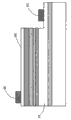
图1显示利用本发明的方式在发光元件上形成波长转换层的结构示意图;Fig. 1 shows a schematic structural view of forming a wavelength conversion layer on a light-emitting element by means of the present invention;
图2显示在波长转换层上形成粗化表面的结构示意图;Fig. 2 shows a schematic diagram of the structure of the roughened surface formed on the wavelength conversion layer;
图3A显示在晶粒切割工艺中形成透明导电层的结构示意图;FIG. 3A shows a schematic diagram of the structure of a transparent conductive layer formed in a die dicing process;
图3B显示在晶粒切割工艺中蚀刻出一凹陷区域的结构示意图;FIG. 3B shows a schematic view of the structure of a recessed region etched in the die dicing process;
图3C显示在晶粒切割工艺中形成n电极与p电极的结构示意图;FIG. 3C shows a schematic diagram of the structure of the n-electrode and the p-electrode formed in the grain cutting process;
图4显示,当外延基板可导电时,n电极可以形成在外延基板的底部的结构示意图;Figure 4 shows, when the epitaxial substrate is conductive, the n-electrode can be formed at the bottom of the epitaxial substrate;
图5A显示在进行外延基板移除过程中形成金属基板的结构示意图;FIG. 5A shows a schematic diagram of the structure of the metal substrate formed during the removal of the epitaxial substrate;
图5B显示在进行外延基板移除过程中移除外延基板与缓冲层的结构示意图;FIG. 5B shows a schematic diagram of removing the epitaxial substrate and the buffer layer during the process of removing the epitaxial substrate;
图5C显示在进行外延基板移除过程中形成n电极与p电极的结构示意图;5C shows a schematic diagram of the structure of n-electrodes and p-electrodes formed during the process of removing the epitaxial substrate;
图6显示本发明也可以应用到倒装芯片封装工艺的结构示意图;FIG. 6 shows a schematic structural view that the present invention can also be applied to a flip-chip packaging process;
图7显示本发明的紫外光元件以及三层波长转换层的混光光谱图;Fig. 7 shows the mixed light spectrum diagram of the ultraviolet light element of the present invention and the three-layer wavelength conversion layer;
图8显示本发明的蓝光元件以及二层波长转换层的混光光谱图;以及Fig. 8 shows the blue light component of the present invention and the light mixing spectrum diagram of two-layer wavelength conversion layer; And
图9显示本发明的蓝光元件以及一层波长转换层的混光光谱图。FIG. 9 shows the mixed light spectrum of the blue light element and a wavelength conversion layer of the present invention.
主要附图标记说明:Explanation of main reference signs:
10外延基板10 epitaxial substrate
11金属基板11 metal substrate
12缓冲层12 buffer layer
14n型导通的包覆层14n-type conduction cladding layer
16有源层16 active layers
18p型导通的电子阻挡层Electron blocking layer for 18p conduction
20p型导通的包覆层20p-type conduction cladding layer
40、42波长转换材料层40, 42 wavelength conversion material layer
60透明导电层60 transparent conductive layer
70凹陷区域70 sunken areas
80、82、84n电极80, 82, 84n electrodes
90、92、94p电极90, 92, 94p electrodes
100封装基板100 Package Substrates
具体实施方式Detailed ways
本发明在此所探讨的方向为一种发光二极管及其工艺。为了能彻底地了解本发明,将在下列的描述中提出详尽的步骤及其组成。显然,本发明的施行并未限定于发光二极管及其工艺的技术人员所熟悉的特殊细节。另一方面,众所周知的组成或步骤并未描述于细节中,以避免造成本发明不必要的限制。本发明的优选实施例会详细描述如下,然而除了这些详细描述的外,本发明还可以广泛地施行在其他的实施例中,且本发明的范围不受限定,其以随附的权利要求为准。The direction of the present invention discussed here is a light emitting diode and its technology. In order to provide a thorough understanding of the present invention, detailed steps and components thereof will be set forth in the following description. Obviously, the practice of the invention is not limited to the specific details familiar to those skilled in light emitting diodes and their art. On the other hand, well-known components or steps have not been described in detail so as not to unnecessarily limit the invention. Preferred embodiments of the present invention will be described in detail as follows, however, in addition to these detailed descriptions, the present invention can also be widely implemented in other embodiments, and the scope of the present invention is not limited, it is based on the appended claims .
本发明利用成长至少一个波长转换材料于发光元件表面,将部分来自发光元件的光转换为至少一种不同波长的光,再与来自发光元件但未经转换的光进行混光的过程,最终得到所需的CIE坐标的光源。The present invention utilizes the process of growing at least one wavelength conversion material on the surface of the light-emitting element, converting part of the light from the light-emitting element into at least one light of different wavelengths, and then mixing light with the unconverted light from the light-emitting element, and finally obtains The desired CIE coordinates of the light source.
本发明提供一种多波长发光二极管,包含一基板、一化合物半导体复合层位于该基板上以及一第一波长转换层位于该化合物半导体复合层上。前述的化合物半导体复合层包含一N型导电的半导体层、一P型导电的半导体层以及一有源层位于N型导电的半导体层与P型导电的半导体层的间,且有源层可激发出一第一波长的激发光。前述的第一半导体波长转换层吸收部分的有源层的第一波长的激发光而放射出一第二波长的激发光,而第二波长大于第一波长。The invention provides a multi-wavelength light-emitting diode, which includes a substrate, a compound semiconductor compound layer on the substrate, and a first wavelength conversion layer on the compound semiconductor compound layer. The aforementioned compound semiconductor composite layer comprises an N-type conductive semiconductor layer, a P-type conductive semiconductor layer, and an active layer located between the N-type conductive semiconductor layer and the P-type conductive semiconductor layer, and the active layer can excite Excitation light of a first wavelength is emitted. The aforesaid first semiconductor wavelength conversion layer absorbs the excitation light of the first wavelength in part of the active layer and emits the excitation light of a second wavelength, and the second wavelength is greater than the first wavelength.
本发明同时提供一种制造多波长发光二极管的方法,包含先提供一外延基板,随后形成一化合物半导体复合层位于外延基板上,然后形成一第一波长转换层位于该化合物半导体复合层上。其中的化合物半导体复合层包含一N型导电的半导体层、一P型导电的半导体层以及一有源层位于N型导电的半导体层与P型导电的半导体层的间,且有源层可激发出一第一波长的激发光。其中的第一半导体波长转换层吸收部分的有源层的第一波长的激发光而放射出一第二波长的激发光,而第二波长大于第一波长。The invention also provides a method for manufacturing a multi-wavelength light-emitting diode, which includes firstly providing an epitaxial substrate, then forming a compound semiconductor compound layer on the epitaxial substrate, and then forming a first wavelength conversion layer on the compound semiconductor compound layer. The compound semiconductor compound layer includes an N-type conductive semiconductor layer, a P-type conductive semiconductor layer, and an active layer located between the N-type conductive semiconductor layer and the P-type conductive semiconductor layer, and the active layer can excite Excitation light of a first wavelength is emitted. The first semiconductor wavelength conversion layer absorbs part of the active layer's excitation light of the first wavelength and emits an excitation light of the second wavelength, and the second wavelength is greater than the first wavelength.
其中上述的第一波长转换层的材料可为III-V族化合物半导体材料或是II-VI族化合物半导体材料,上述的III-V族化合物半导体材料可为III族氮化合物、III族磷化合物或是III族砷化合物。并且,上述的第一波长转换层的表面可为粗化表面。Wherein the material of the above-mentioned first wavelength conversion layer can be a III-V group compound semiconductor material or a II-VI group compound semiconductor material, and the above-mentioned III-V group compound semiconductor material can be a III-group nitrogen compound, a III-group phosphorus compound or It is a group III arsenic compound. In addition, the surface of the above-mentioned first wavelength conversion layer may be a roughened surface.
本发明同时包含一第二波长转换层位于第一波长转换层上,其中的可导电的半导体波长转换层吸收部分有源层的第一波长的激发光及第一波长转换材料的第二波长的激发光而放射出一第三波长的激发光,而第三波长大于第二波长。上述的第二波长转换层可为III族氮化合物、III族磷化合物或是III族砷化合物。The present invention also includes a second wavelength conversion layer located on the first wavelength conversion layer, wherein the conductive semiconductor wavelength conversion layer absorbs part of the excitation light of the first wavelength of the active layer and the excitation light of the second wavelength of the first wavelength conversion material. The excitation light emits an excitation light with a third wavelength, and the third wavelength is greater than the second wavelength. The above-mentioned second wavelength conversion layer can be a group III nitrogen compound, a group III phosphorus compound or a group III arsenic compound.
上述的II-VI族化合物半导体材料可为II族氧化合物、II族硫化合物或是II族硒化合物。The aforementioned group II-VI compound semiconductor materials can be group II oxygen compounds, group II sulfur compounds or group II selenium compounds.
上述的基板可为蓝宝石(Al2O3)基板、碳化硅(SiC)基板、铝酸锂基板(AlLiO2)、镓酸锂基板(LiGaO2)、硅(Si)基板、氮化镓(GaN)基板,氧化锌(ZnO)基板、氧化铝锌基板(AlZnO)、砷化镓(GaAs)基板、磷化镓(GaP)基板、锑化镓基板(GaSb)、磷化铟(InP)基板、砷化铟(InAs)基板、硒化锌(ZnSe)基板或是金属基板。本发明同时包含一缓冲层位于上述基板与化合物半导体复合层之间。本发明同时包含一P型导电的电子阻挡层位于有源层与P型导电的半导体层之间。再者,本发明同时包含一透明导电层位于上述第一或第二波长转换层上,且与第一或第二波长转换层欧姆接触。The above-mentioned substrates can be sapphire (Al2O3) substrates, silicon carbide (SiC) substrates, lithium aluminate substrates (AlLiO2), lithium gallate substrates (LiGaO2), silicon (Si) substrates, gallium nitride (GaN) substrates, zinc oxide (ZnO) substrate, aluminum zinc oxide substrate (AlZnO), gallium arsenide (GaAs) substrate, gallium phosphide (GaP) substrate, gallium antimonide substrate (GaSb), indium phosphide (InP) substrate, indium arsenide (InAs) ) substrate, zinc selenide (ZnSe) substrate or metal substrate. The present invention also includes a buffer layer located between the substrate and the compound semiconductor compound layer. The present invention also includes a P-type conductive electron blocking layer located between the active layer and the P-type conductive semiconductor layer. Furthermore, the present invention also includes a transparent conductive layer located on the first or second wavelength conversion layer and in ohmic contact with the first or second wavelength conversion layer.
上述的外延基板可为蓝宝石基板、碳化硅基板、铝酸锂基板、镓酸锂基板、硅基板、氮化镓基板、氧化锌基板、氧化铝锌基板、砷化镓基板、磷化镓基板、锑化镓基板、磷化铟基板、砷化铟基板或是硒化锌基板。本发明同时包含形成一缓冲层位于外延基板与化合物半导体复合层之间。本发明同时包含形成一P型导电的电子阻挡层位于有源层与P型导电的半导体层之间。再者,本发明同时包含形成一透明导电层位于该第一波长转换层上,且与可导电的波长转换层欧姆接触。The aforementioned epitaxial substrates can be sapphire substrates, silicon carbide substrates, lithium aluminate substrates, lithium gallate substrates, silicon substrates, gallium nitride substrates, zinc oxide substrates, aluminum zinc oxide substrates, gallium arsenide substrates, gallium phosphide substrates, Gallium antimonide substrate, indium phosphide substrate, indium arsenide substrate or zinc selenide substrate. The invention also includes forming a buffer layer between the epitaxial substrate and the compound semiconductor compound layer. The present invention also includes forming a P-type conductive electron blocking layer between the active layer and the P-type conductive semiconductor layer. Moreover, the present invention also includes forming a transparent conductive layer on the first wavelength conversion layer and in ohmic contact with the conductive wavelength conversion layer.
本发明同时包含形成一欧姆导电层位于该第一波长转换层上,且与可导电的波长转换层欧姆接触。本发明同时包含形成一金属基板于欧姆导电层上。本发明同时包含移除该外延基板的步骤。The invention also includes forming an ohmic conductive layer on the first wavelength conversion layer and in ohmic contact with the conductive wavelength conversion layer. The invention also includes forming a metal substrate on the ohmic conductive layer. The present invention also includes the step of removing the epitaxial substrate.
上述的实施内容,将会搭配图示与各步骤的结构示意图以详细介绍本发明的结构与形成方式的各步骤。The above implementation content will be combined with diagrams and structural schematic diagrams of each step to introduce the structure and each step of the formation method of the present invention in detail.
请参照图1,首先提供一外延基板10,其中外延基板10可以使用下列几种,蓝宝石基板、碳化硅基板、铝酸锂基板、镓酸锂基板、硅基板、氮化镓基板、氧化锌基板、氧化铝锌基板、砷化镓基板、磷化镓基板、锑化镓基板、磷化铟基板、砷化铟基板或是硒化锌基板等。外延基板的选择,主要在于外延的材料的选择。举例来说,一般II-VI半导体化合物会使用硒化锌基板或是氧化锌基板做为外延基材;III-砷化物或是磷化物通常是使用砷化镓基板、磷化镓基板、磷化铟基板或是砷化铟基板;而III-氮化物在商业上通常会使用蓝宝石基板或是碳化硅基板,目前实验阶段有使用铝酸锂基板、镓酸锂基板、硅基板或是氧化铝锌基板等。另外,晶格结构与晶格常数是另一项选择外延基板的重要依据。晶格常数差异过大,往往需要先形成一缓冲层才可以得到优选的外延品质。在本实施例中,使用的外延材料为III-氮化物,特别是使用氮化镓,而搭配使用的外延基板是目前商业上常见的蓝宝石基板或是碳化硅基板。然而,任何本领域的普通技术人员应能理解,本发明的外延材料的选择并不限定于III-氮化物,或甚至是氮化镓等的材料。任何III-V半导体化合物或是II-VI半导体化合物皆可应用在本发明中。Please refer to Fig. 1, first provide an
一种改善后续外延品质的方式,是在外延基板10上先形成图案,使得之后外延的过程中,缺陷密度不会顺着外延的方向向上成长,最后通过有源层。不同的图案设计,会对应到各种不同的外延条件与外延品质。涉及具有图案的外延基板的外延技术,可以参阅先进开发光电之前的专利申请提案,中国台湾专利申请号096150701。One way to improve the quality of subsequent epitaxy is to form a pattern on the
由于使用蓝宝石基板或是碳化硅基板,在外延III-氮化物之前需要先形成一缓冲层12,这是因为蓝宝石基板与氮化镓之间的晶格常数的不匹配高达14%,而使用碳化硅基板也有达到3.5%的晶格常数的不匹配。一般的缓冲层12的材料可以是氮化镓、氮化铝镓(AlGaN)、氮化铝(AlN)、或是InGaN/InGaN超晶格结构。涉及形成InGaN/InGaN超晶格结构的技术,可以参阅先进开发光电之前的专利申请提案,中国台湾专利申请号096104378。形成缓冲层12的方式是在外延机台,例如有机金属化学气相沉积(MOCVD;Metal OrganicChemical Vapor Deposition)机台或是分子束外延(MBE;Molecular BeamEpitaxy)机台中,以相对于后续正常外延温度较低的环境长晶。例如氮化铝镓铟的一般长晶温度约在800-1400℃之间,而缓冲层的长晶温度约在250-700℃之间。当使用有机金属化学气相沉积机台时,氮的先驱物可以是NH3或是N2,镓的先驱物可以是三甲基镓或是三乙基镓,而铝的先驱物可以是三甲基铝或是三乙基铝。反应室的压力可以是低压或是常压。Due to the use of a sapphire substrate or a silicon carbide substrate, a
随后形成n型导通的氮化镓层或是氮化铝镓层,而这一层的作用是提供发光二极管的n型导通的包覆层(cladding layer)14。n型导通的氮化镓层或是氮化铝镓层的形成方式,是在有机金属化学气相沉积机台或是分子束外延机台中,在形成氮化物层时,同时掺杂四族的原子,在本实施例中是硅原子,而硅的先驱物在有机金属化学气相沉积机台中可以是硅甲烷或是硅乙烷。在这一层的下方可以在缓冲层上先行依续形成未参杂的氮化镓层(未在图示中显示)以及n型导通的接触层(未在图示中显示),而这两层的形成步骤是非必需的(optional)。形成未参杂的氮化镓层是提升n型导通的包覆层的外延品质,而n型导通的接触层是高掺杂的氮化镓层或是氮化铝镓层,可以提供与n型电极之间优选的导电效果。Subsequently, an n-type conduction GaN layer or an AlGaN layer is formed, and the function of this layer is to provide an n-type conduction cladding layer (cladding layer) 14 of the light emitting diode. The n-type conduction gallium nitride layer or aluminum gallium nitride layer is formed by doping the four groups simultaneously in the metalorganic chemical vapor deposition machine or molecular beam epitaxy machine when the nitride layer is formed. Atoms, in this embodiment, are silicon atoms, and the precursor of silicon in the metalorganic chemical vapor deposition tool can be silane or silethane. Under this layer, an undoped gallium nitride layer (not shown in the figure) and an n-type conduction contact layer (not shown in the figure) can be successively formed on the buffer layer, and this The step of forming two layers is optional. The formation of undoped gallium nitride layer is to improve the epitaxial quality of the cladding layer of n-type conduction, and the contact layer of n-type conduction is a highly doped gallium nitride layer or aluminum gallium nitride layer, which can provide Excellent conduction effect with n-type electrodes.
接着是形成一有源层16在n型导通的包覆层14上,其中有源层16是发光二极管元件的发光层,可以是单异质结构、双异质结构、单量子阱层或是多重量子阱层结构。目前多采用多重量子阱层结构,也就是多重量子阱层/阻障层的结构。量子阱层可以使用氮化铟镓,而阻障层可以使用氮化铝镓等的三元结构。另外,也可以采用四元结构,也就是使用氮化铝镓铟(AlxInyGal-x-yN)同时作为量子阱层以及阻障层,其中调整铝与铟的比例使得氮化铝镓铟晶格的能阶可以分别成为高能阶的阻障层与低能阶的量子阱层。有源层的形成方式,基本上接近前述的形成n型导通的包覆层的方式,其中铟的先驱物可以是三甲基铟或是三乙基铟。有源层可以掺杂n型或是p型的掺杂子(dopant),可以是同时掺杂n型与p型的掺杂子,也可以完全不掺杂。并且,可以是量子阱层掺杂而阻障层不掺杂、量子阱层不掺杂而阻障层掺杂、量子阱层与阻障层都掺杂或是量子阱层与阻障层都不掺杂。再者,亦可以在量子阱层的部分区域进行高浓度的掺杂(delta doping)。Next is to form an
之后,在有源层上可以形成一p型导通的电子阻挡层18,这个步骤可以是非必需的(optional)。p型导通的电子阻挡层18可包括第一种三五族半导体层,以及第二种三五族半导体层。这两种三五族半导体层,能隙不同,且具有周期性地重复沉积在上述有源发光层上,以作为一势垒较高的电子阻挡层(势垒高于有源发光层的势垒),用以阻挡过多电子(e-)溢流有源发光层。关于p型导通的电子阻挡层18详细的内容与形成方式,可以参阅先进开发光电之前的专利申请提案,中国台湾专利申请号097128065。Afterwards, a p-type conduction
接着,形成一p型导通的氮化镓层或是氮化铝镓层,而这一层的作用是提供发光二极管的p型导通的包覆层(cladding layer)20。p型导通的氮化镓层或是氮化铝镓层的形成方式,是在有机金属化学气相沉积机台或是分子束外延机台中,在形成氮化物层时,同时掺杂二族的原子,在本实施例中是镁原子,而镁的先驱物在有机金属化学气相沉积机台中可以是CP2Mg。在这一层的上方可以形成p型导通的接触层(未在图示中显示),而这层的形成步骤是非必需的(optional)。p型导通的接触层是高掺杂的氮化镓层或是氮化铝镓层,可以提供与p型电极之间优选的导电效果。Next, a p-type conduction GaN layer or AlGaN layer is formed, and the function of this layer is to provide a p-type conduction cladding layer (cladding layer) 20 of the LED. The formation method of the p-type conduction gallium nitride layer or aluminum gallium nitride layer is to dope the second group simultaneously when forming the nitride layer in the organic metal chemical vapor deposition machine or the molecular beam epitaxy machine. Atom, in this embodiment is a magnesium atom, and the precursor of magnesium in the organometallic chemical vapor deposition machine can be CP2Mg. A p-type conductive contact layer (not shown in the figure) may be formed above this layer, and the formation step of this layer is optional. The p-type conductive contact layer is a highly doped gallium nitride layer or aluminum gallium nitride layer, which can provide a preferred conductive effect with the p-type electrode.
然后,形成一波长转换材料层40在p型导通的包覆层20或是p型导通的接触层上。波长转换材料层40可以是III-V族化合物半导体材料或是II-VI族化合物半导体材料,例如AlInGaAs、GaAs、InAs、AlAs、InGaAs、AlGaAs、InAlAs,AlInGaP、GaP、InP、AlP、InGaP、AlGaP、InAlP、AlInGaN、GaN、InN、AlN、InGaN、AlGaN、InAlN、ZnSe、ZnMgBeSSe、ZnCdSe、ZnMgSe、ZnSSe、ZrAgSSe、ZnMgSSe、ZnCdSe/ZnMgSSe或是ZnMgBeSe/ZnCdSe/ZnMgBeSe。波长转换材料的形成方式,无论是III-V族化合物半导体材料或是II-VI族化合物半导体材料,都可以使用有机金属化学气相沉积法,分子束外延法,或是使用晶片接合(wafer bonding)法,其中晶片接合的方式可以将已经形成好的波长转换材料层直接黏接在p型导通的包覆层或是p型导通的接触层。在本发明中,波长转换材料层可以经由掺杂而具有p型导通。这样可以降低波长转换材料层在电性上的阻抗。Then, a wavelength
由于发光元件中的有源层会由电子空穴的结合而激发第一激发辐射光,而一部分的第一激发辐射光会激发光转换材料层而得到第二激发辐射光。调整有源层的能阶与光转换材料层的能阶可以得到任何所需CIE坐标的固态发光元件或是可以得到演色性(Ra)佳的白光光源。Since the active layer in the light-emitting element will excite the first excitation radiation light due to the combination of electrons and holes, and a part of the first excitation radiation light will excite the photo-conversion material layer to obtain the second excitation radiation light. Adjusting the energy level of the active layer and the energy level of the light conversion material layer can obtain any desired CIE coordinate solid-state light-emitting device or a white light source with good color rendering (Ra).
在本发明中,波长转换材料可以是一层或是一层以上。并且可以根据材料的不同进行不同的组合与搭配。例如,一层波长转换材料是III-V族化合物半导体材料而另一层是II-VI族化合物半导体材料,或是两层都是III-V族化合物半导体材料或是II-VI族化合物半导体材料。另外,波长转换层的表面可为粗化表面。In the present invention, the wavelength converting material may be one layer or more than one layer. And it can be combined and matched according to different materials. For example, one layer of wavelength conversion material is a III-V compound semiconductor material and the other layer is a II-VI compound semiconductor material, or both layers are III-V compound semiconductor materials or II-VI compound semiconductor materials . In addition, the surface of the wavelength conversion layer may be a roughened surface.
在本发明的一实施例中,有源层是InGaN/AlGaN多重量子阱层,并且可以发射出紫外光或是近紫外光,其波长约在365-420纳米之间,请参阅图7。波长转换材料可以有三层,第一波长转换材料层是InGaN,可以发射出蓝光,波长约在440-480纳米之间;第二波长转换材料层是InGaN,可以发射出绿光或是黄绿光,波长约在480-570纳米之间;第三波长转换材料层是可以GaP、GaAs、或是InN,可以发射出黄光或是红光,波长约在580-650纳米之间。In an embodiment of the present invention, the active layer is an InGaN/AlGaN multiple quantum well layer, and can emit ultraviolet light or near ultraviolet light with a wavelength of about 365-420 nm, please refer to FIG. 7 . The wavelength conversion material can have three layers. The first wavelength conversion material layer is InGaN, which can emit blue light with a wavelength of about 440-480 nanometers; the second wavelength conversion material layer is InGaN, which can emit green light or yellow-green light. about 480-570 nanometers; the third wavelength conversion material layer can be GaP, GaAs, or InN, and can emit yellow or red light with a wavelength between about 580-650 nanometers.
在本发明的另一实施例中,有源层是InGaN/AlGaN多重量子阱层,并且可以发射出蓝光,其波长约在440-460纳米之间,请参阅图8。波长转换材料可以有两层,第一波长转换材料层是InGaN,可以发射出绿光或是黄绿光,波长约在480-570纳米之间;第二波长转换材料层可以是GaP、GaAs或是InN,可以发射出黄光或是红光,波长约在580-650纳米之间。In another embodiment of the present invention, the active layer is an InGaN/AlGaN multiple quantum well layer, and can emit blue light with a wavelength between about 440-460 nm, please refer to FIG. 8 . The wavelength conversion material can have two layers, the first wavelength conversion material layer is InGaN, which can emit green light or yellow-green light, and the wavelength is about 480-570 nanometers; the second wavelength conversion material layer can be GaP, GaAs or InN , can emit yellow or red light with a wavelength of about 580-650 nanometers.
在本发明的另一实施例中,有源层是InGaN/AlGaN多重量子阱层,并且可以发射出蓝光,其波长约在440-460纳米之间,请参阅图9。波长转换材料有一层,波长转换材料层可以是GaP、GaAs或是InN,可以发射出黄光或是红光,波长约在520-650纳米之间。在这个实施例中,在最后的封装阶段可以混合黄色光或是绿色光的荧光粉,使得封装完成的发光二极管元件可以发射出高演色性的白光。In another embodiment of the present invention, the active layer is an InGaN/AlGaN multiple quantum well layer, and can emit blue light with a wavelength between about 440-460 nm, please refer to FIG. 9 . The wavelength conversion material has a layer, and the wavelength conversion material layer can be GaP, GaAs or InN, which can emit yellow light or red light with a wavelength of about 520-650 nanometers. In this embodiment, yellow or green phosphors can be mixed in the final packaging stage, so that the packaged light-emitting diode element can emit white light with high color rendering.
请参阅图2,当波长转换材料层42为不导电时,必须将透明导电层60与p型导通的包覆层20或是p型导通的接触层直接接触,产生电性连接。最简单的方式,是以蚀刻的方式移除一部分的波长转换材料层42,或是在有机金属化学气相沉积中利用外延的条件直接形成未完全覆盖的波长转换材料层42。其中,蚀刻可以采用湿式蚀刻或是干式蚀刻。Please refer to FIG. 2 , when the wavelength
接下来的工艺是属于发光二极管的晶粒切割工艺。首先,请参阅图3A,形成一透明导电层60在波长转换材料层上,其中透明导电层60必须与波长转换材料层40之间形成欧姆接触。透明导电层60的材质可以是Ni/Au、ITO、IZO、IWO或是IGO等可以跟p型导通的III-氮化物之间欧姆接触的材料。透明导电层60的形成方式,可以是蒸镀,溅镀等物理气相沉积法。The next process is the die cutting process belonging to the LED. First, referring to FIG. 3A , a transparent
接着,当外延基板是蓝宝石基板或是不导电的基板时,会在同一面形成n电极与p电极的同面电极的结构,如图3C所示。在这个工艺步骤中,首先需要将一部分的透明导电层60、波长转换材料层40、p型导通的接触层(如果有形成)、p型导通的包覆层20、有源层16、n型导通的包覆层14以及n型导通的接触层(如果有形成)移除,以形成一凹陷区域70,请参阅图3B。移除的方式可以使用干式蚀刻或是湿式蚀刻的方式。然后,请参阅图3C,分别在透明导电层60上形成p电极90,在露出的n型导通的包覆层14或是n型导通的接触层(如果有形成)上形成n电极80。n电极80与p电极90的形成的方式可以使用蒸镀或是溅镀等的物理气相沉积法。上述n电极80与p电极90的工艺可以透过光刻或是剥离(lift-off)方式形成图案。Next, when the epitaxial substrate is a sapphire substrate or a non-conductive substrate, an n-electrode and a p-electrode structure are formed on the same surface, as shown in FIG. 3C . In this process step, first, a part of the transparent
形成电极之后,会对外延基板进行研磨的步骤,将蓝宝石基板的厚度降低。基本上这个步骤是非必需的(optional),主要的目的是可以提升元件的发光亮度。After the electrodes are formed, the epitaxial substrate will be polished to reduce the thickness of the sapphire substrate. Basically, this step is optional, and the main purpose is to improve the luminance of the component.
当外延基板是碳化硅或是其他的导电基板时,可以不用对一部分的透明导电层、波长转换材料层、p型导通的接触层(如果有形成)、p型导通的包覆层、有源层、n型导通的包覆层以及n型导通的接触层(如果有形成)移除以露出n型导通的包覆层或是n型导通的接触层(如果有形成)。请参阅图4,n电极82可以直接形成在外延基板10的底部,而p电极92会形成在透明导电层60上接近中央的区域。When the epitaxial substrate is silicon carbide or other conductive substrates, part of the transparent conductive layer, wavelength conversion material layer, p-type conductive contact layer (if formed), p-type conductive cladding layer, The active layer, the cladding layer of n-type conduction and the contact layer of n-type conduction (if formed) are removed to expose the clad layer of n-type conduction or the contact layer of n-type conduction (if formed) ). Referring to FIG. 4 , the n-
另外,当外延基板是蓝宝石基板时,也可以使用基板剥离(substrate lift-off)技术,将蓝宝石基板给完全移除,请参阅图5。这时,需要在另一面形成另一个可支撑晶片应力的金属基板11,才能将蓝宝石基板移除,如图5A所示。当使用基板剥离技术时,在波长转换材料层之后形成的欧姆接触层60,可以不需要是透明的。基板剥离技术可以使用激光热分离的技术,或是使用化学蚀刻的技术将外延基板10与缓冲层12移除,如图5B所示。随后,如图5C所示,整个晶片会反置使得n型导通的包覆层14会朝上。在金属基板11下形成p电极94,在n型导通的包覆层14上形成n电极84。不论是使用导电的外延基板或是使用基板剥离技术,都可形成双面的n电极与-p电极。In addition, when the epitaxial substrate is a sapphire substrate, the substrate lift-off technique can also be used to completely remove the sapphire substrate, as shown in Figure 5. At this time, another
随后,就会对整片的晶片进行切割形成晶粒。晶片切割的方式可以使用切割刀或是使用激光将整个晶片切割成一个个小块的晶粒(chip)或是晶方(die)。切割下来的晶粒或是晶方都会黏在蓝膜上供下一阶段的封装工艺用。Subsequently, the entire wafer is diced to form dies. Wafer dicing can use a dicing knife or a laser to cut the entire wafer into small pieces of crystal grains (chips) or crystal cubes (die). The cut dies or wafers will be stuck on the blue film for the next stage of packaging process.
本发明亦可以应用到倒装芯片(flip-chip)封装的型态,请参阅图6。在晶粒切割的工艺中,就只能形成同面电极的结构。然后在封装的工艺中,直接将同面电极结构的晶粒或是晶方的n电极与p电极直接黏着到封装基板100上。The present invention can also be applied to flip-chip packaging, please refer to FIG. 6 . In the grain cutting process, only the structure of electrodes on the same plane can be formed. Then, in the packaging process, the crystal grains of the same-plane electrode structure or the n-electrode and p-electrode of the crystal square are directly adhered to the
本发明利用成长至少一个波长转换材料层于发光元件表面的手段,达成可以直接发出白光或是多波长激发光的功效,其中波长转换材料为半导体,可任意改变所需要的波长。而且,在封装工艺的阶段可以不需要添加荧光粉就可以发射出白光,或是可以提供高演色性的白光。The present invention uses the method of growing at least one wavelength conversion material layer on the surface of the light-emitting element to achieve the effect of directly emitting white light or multi-wavelength excitation light. The wavelength conversion material is a semiconductor, and the required wavelength can be changed arbitrarily. Moreover, at the stage of packaging process, white light can be emitted without adding phosphor powder, or white light with high color rendering property can be provided.
从本发明手段与具有的功效中,可以得到本发明具有诸多的优点。首先,形成的波长转换材料层的全工艺可以于外延反应器内完成,不需额外的黄光光刻工艺,减少外延片受污染的机会。另外,相较于诸多的现有技术中,发光元件的p-n结位置不会改变,可保留原发光元件的发光效率。再者,波长转换材料为化合物半导体,可根据材料的能阶任意改变所需要的波长。同时,可对波长转换材料层形成具有粗化的表面,因而增加元件的光取出效率。From the means and effects of the present invention, it can be obtained that the present invention has many advantages. First, the entire process of forming the wavelength conversion material layer can be completed in the epitaxial reactor, without the need of additional photolithography process, reducing the chance of contamination of the epitaxial wafer. In addition, compared with many existing technologies, the position of the p-n junction of the light-emitting element will not change, and the luminous efficiency of the original light-emitting element can be retained. Furthermore, the wavelength conversion material is a compound semiconductor, and the required wavelength can be changed arbitrarily according to the energy level of the material. At the same time, the wavelength conversion material layer can be formed to have a roughened surface, thereby increasing the light extraction efficiency of the element.
显然,依照上面实施例中的描述,本发明可能有许多的修正与差异。因此需要在其附加的权利要求的范围内加以理解,除了上述详细的描述外,本发明还可以广泛地在其他的实施例中施行。上述仅为本发明的优选实施例而已,并非用以限定本发明;凡其它未脱离本发明所公开的精神下所完成的修改,均应包含在所附权利要求所要求保护的范围内。Obviously, according to the description in the above embodiments, the present invention may have many modifications and differences. It is therefore to be understood, within the scope of the appended claims, that the invention may be practiced broadly in other embodiments than the foregoing detailed description. The above are only preferred embodiments of the present invention, and are not intended to limit the present invention; any other modifications that do not deviate from the disclosed spirit of the present invention should be included in the scope of protection required by the appended claims.
Claims (11)
Priority Applications (1)
| Application Number | Priority Date | Filing Date | Title |
|---|---|---|---|
| CN200810167918A CN101728462A (en) | 2008-10-17 | 2008-10-17 | Multi-wavelength light emitting diode and manufacturing method thereof |
Applications Claiming Priority (1)
| Application Number | Priority Date | Filing Date | Title |
|---|---|---|---|
| CN200810167918A CN101728462A (en) | 2008-10-17 | 2008-10-17 | Multi-wavelength light emitting diode and manufacturing method thereof |
Publications (1)
| Publication Number | Publication Date |
|---|---|
| CN101728462A true CN101728462A (en) | 2010-06-09 |
Family
ID=42449028
Family Applications (1)
| Application Number | Title | Priority Date | Filing Date |
|---|---|---|---|
| CN200810167918A Pending CN101728462A (en) | 2008-10-17 | 2008-10-17 | Multi-wavelength light emitting diode and manufacturing method thereof |
Country Status (1)
| Country | Link |
|---|---|
| CN (1) | CN101728462A (en) |
Cited By (10)
| Publication number | Priority date | Publication date | Assignee | Title |
|---|---|---|---|---|
| CN102428579A (en) * | 2009-05-29 | 2012-04-25 | 欧司朗光电半导体有限公司 | Optoelectronic semiconductor chip and method for producing an optoelectronic semiconductor chip |
| CN102956766A (en) * | 2011-08-22 | 2013-03-06 | 隆达电子股份有限公司 | Method for manufacturing light-emitting diode device and light-emitting semiconductor structure |
| CN102956781A (en) * | 2011-08-31 | 2013-03-06 | 新世纪光电股份有限公司 | Light emitting element and manufacturing method thereof |
| WO2013033969A1 (en) * | 2011-09-07 | 2013-03-14 | SemiLEDs Optoelectronics Co., Ltd. | Systems and methods for producing white-light light emitting diodes |
| CN103456858A (en) * | 2012-05-28 | 2013-12-18 | 新世纪光电股份有限公司 | Light emitting element and method for manufacturing the same |
| CN105518881B (en) * | 2013-09-16 | 2019-04-16 | 奥斯兰姆施尔凡尼亚公司 | Thin film wavelength converter and method for manufacturing thin film wavelength converter |
| TWI657931B (en) * | 2016-11-15 | 2019-05-01 | 迎輝科技股份有限公司 | Optical film |
| CN110911533A (en) * | 2019-12-03 | 2020-03-24 | 泗阳群鑫电子有限公司 | Semiconductor light-emitting element wafer and manufacturing method thereof |
| CN112086548A (en) * | 2018-07-16 | 2020-12-15 | 厦门三安光电有限公司 | Micro-light emitting device and display thereof |
| WO2021197101A1 (en) * | 2020-04-03 | 2021-10-07 | 华为技术有限公司 | Led device and manufacturing method therefor, display module, and terminal |
-
2008
- 2008-10-17 CN CN200810167918A patent/CN101728462A/en active Pending
Cited By (15)
| Publication number | Priority date | Publication date | Assignee | Title |
|---|---|---|---|---|
| CN102428579A (en) * | 2009-05-29 | 2012-04-25 | 欧司朗光电半导体有限公司 | Optoelectronic semiconductor chip and method for producing an optoelectronic semiconductor chip |
| US9306131B2 (en) | 2009-05-29 | 2016-04-05 | Osram Opto Semiconductors Gmbh | Optoelectronic semiconductor chip and method of producing an optoelectronic semiconductor chip |
| US8900888B2 (en) | 2009-05-29 | 2014-12-02 | Osram Opto Semiconductors Gmbh | Optoelectronic semiconductor chip and method for producing an optoelectronic semiconductor chip |
| CN102428579B (en) * | 2009-05-29 | 2015-02-25 | 欧司朗光电半导体有限公司 | Optoelectronic semiconductor chip and method for producing an optoelectronic semiconductor chip |
| CN102956766A (en) * | 2011-08-22 | 2013-03-06 | 隆达电子股份有限公司 | Method for manufacturing light-emitting diode device and light-emitting semiconductor structure |
| CN102956781B (en) * | 2011-08-31 | 2015-03-11 | 新世纪光电股份有限公司 | Light emitting element and manufacturing method thereof |
| CN102956781A (en) * | 2011-08-31 | 2013-03-06 | 新世纪光电股份有限公司 | Light emitting element and manufacturing method thereof |
| WO2013033969A1 (en) * | 2011-09-07 | 2013-03-14 | SemiLEDs Optoelectronics Co., Ltd. | Systems and methods for producing white-light light emitting diodes |
| CN103456858A (en) * | 2012-05-28 | 2013-12-18 | 新世纪光电股份有限公司 | Light emitting element and method for manufacturing the same |
| CN103456858B (en) * | 2012-05-28 | 2016-09-14 | 新世纪光电股份有限公司 | Light emitting element and method for manufacturing the same |
| CN105518881B (en) * | 2013-09-16 | 2019-04-16 | 奥斯兰姆施尔凡尼亚公司 | Thin film wavelength converter and method for manufacturing thin film wavelength converter |
| TWI657931B (en) * | 2016-11-15 | 2019-05-01 | 迎輝科技股份有限公司 | Optical film |
| CN112086548A (en) * | 2018-07-16 | 2020-12-15 | 厦门三安光电有限公司 | Micro-light emitting device and display thereof |
| CN110911533A (en) * | 2019-12-03 | 2020-03-24 | 泗阳群鑫电子有限公司 | Semiconductor light-emitting element wafer and manufacturing method thereof |
| WO2021197101A1 (en) * | 2020-04-03 | 2021-10-07 | 华为技术有限公司 | Led device and manufacturing method therefor, display module, and terminal |
Similar Documents
| Publication | Publication Date | Title |
|---|---|---|
| TWI416757B (en) | Multi-wavelength light-emitting diode and manufacturing method thereof | |
| JP5702739B2 (en) | Boron Introduced Group III Nitride Light Emitting Diode Device | |
| CN102947955B (en) | Ultraviolet semiconductor light-emitting component | |
| CN101728462A (en) | Multi-wavelength light emitting diode and manufacturing method thereof | |
| CN102117771B (en) | LED epitaxial wafer and LED chip as well as manufacturing method thereof | |
| US20220285505A1 (en) | Indium-gallium-nitride structures and devices | |
| WO2010100844A1 (en) | Nitride semiconductor element and method for manufacturing same | |
| US7910154B2 (en) | Nitride-based light emitting devices and methods of manufacturing the same | |
| KR102135836B1 (en) | Method of forming a P-type layer for a light emitting device | |
| KR102147587B1 (en) | Ⅲ-nitride light-emitting device grown on a relaxed layer | |
| CN105633229B (en) | Light-emitting diode and method of making the same | |
| TW201828493A (en) | Method for growing a light-emitting device under ultraviolet light irradiation | |
| KR100661960B1 (en) | Light emitting diodes and manufacturing method thereof | |
| US20090008626A1 (en) | Optoelectronic device | |
| KR101198759B1 (en) | Nitride light emitting device | |
| US20220181516A1 (en) | Mixed color light emitting device | |
| KR102302320B1 (en) | Light emitting device | |
| JP3540643B2 (en) | Method for manufacturing semiconductor device | |
| KR101241331B1 (en) | Nitride based LED and method of manufacturing the same | |
| KR100608919B1 (en) | Light emitting device and manufacturing method thereof | |
| KR100699057B1 (en) | Light emitting device and manufacturing method | |
| KR101198760B1 (en) | LED having vertical structure and method of making the same | |
| KR101414652B1 (en) | Nitride semiconductor light emitting device | |
| KR101414654B1 (en) | Nitride semiconductor light emitting device | |
| KR20080089904A (en) | Nitride semiconductor light emitting device and manufacturing method |
Legal Events
| Date | Code | Title | Description |
|---|---|---|---|
| C06 | Publication | ||
| PB01 | Publication | ||
| C10 | Entry into substantive examination | ||
| SE01 | Entry into force of request for substantive examination | ||
| ASS | Succession or assignment of patent right |
Owner name: ZHANJING TECHNOLOGY (SHENZHEN) CO., LTD. Free format text: FORMER OWNER: ADVANCED DEVELOPMENT PHOTOELECTRIC CO., LTD. Effective date: 20101117 Owner name: RONGCHUANG ENERGY TECHNOLOGY CO., LTD. |
|
| C41 | Transfer of patent application or patent right or utility model | ||
| COR | Change of bibliographic data |
Free format text: CORRECT: ADDRESS; FROM: HSINCHU COUNTY, TAIWAN PROVINCE, CHINA TO: NO. 2, E. RING ROAD 2, INDUSTRY ZONE 10, YOUSONG, LONGHUA SUBDISTRICT OFFICE, BAO AN DISTRICT, SHENZHEN CITY, GUANGDONG PROVINCE |
|
| TA01 | Transfer of patent application right |
Effective date of registration: 20101117 Address after: No. two, No. 2, East Ring Road, Pinus tabulaeformis Industrial Zone, Longhua, Baoan District, Shenzhen, Guangdong, Applicant after: Zhanjing Technology (Shenzhen) Co., Ltd. Co-applicant after: Advanced Optoelectronic Technology Inc. Address before: Hsinchu County, Taiwan, China Applicant before: Advanced Development Photoelectric Co., Ltd. |
|
| C02 | Deemed withdrawal of patent application after publication (patent law 2001) | ||
| WD01 | Invention patent application deemed withdrawn after publication |
Open date: 20100609 |