[go: up one dir, main page]

CN101682126A - Electrical connector for use in soldering operations - Google Patents

Electrical connector for use in soldering operations Download PDF

Info

Publication number
CN101682126A
CN101682126A CN200880013738A CN200880013738A CN101682126A CN 101682126 A CN101682126 A CN 101682126A CN 200880013738 A CN200880013738 A CN 200880013738A CN 200880013738 A CN200880013738 A CN 200880013738A CN 101682126 A CN101682126 A CN 101682126A
Authority
CN
China
Prior art keywords
electronic circuit
solder
groove
solder segment
scolder
Prior art date
Legal status (The legal status is an assumption and is not a legal conclusion. Google has not performed a legal analysis and makes no representation as to the accuracy of the status listed.)
Granted
Application number
CN200880013738A
Other languages
Chinese (zh)
Other versions
CN101682126B (en
Inventor
詹姆斯·R·泽诺利
约瑟夫·S·卡奇纳
Current Assignee (The listed assignees may be inaccurate. Google has not performed a legal analysis and makes no representation or warranty as to the accuracy of the list.)
Teka Interconnection Systems Inc
Original Assignee
Teka Interconnection Systems Inc
Priority date (The priority date is an assumption and is not a legal conclusion. Google has not performed a legal analysis and makes no representation as to the accuracy of the date listed.)
Filing date
Publication date
Application filed by Teka Interconnection Systems Inc filed Critical Teka Interconnection Systems Inc
Publication of CN101682126A publication Critical patent/CN101682126A/en
Application granted granted Critical
Publication of CN101682126B publication Critical patent/CN101682126B/en
Active legal-status Critical Current
Anticipated expiration legal-status Critical

Links

Images

Classifications

    • BPERFORMING OPERATIONS; TRANSPORTING
    • B23MACHINE TOOLS; METAL-WORKING NOT OTHERWISE PROVIDED FOR
    • B23KSOLDERING OR UNSOLDERING; WELDING; CLADDING OR PLATING BY SOLDERING OR WELDING; CUTTING BY APPLYING HEAT LOCALLY, e.g. FLAME CUTTING; WORKING BY LASER BEAM
    • B23K1/00Soldering, e.g. brazing, or unsoldering
    • B23K1/0008Soldering, e.g. brazing, or unsoldering specially adapted for particular articles or work
    • B23K1/0016Brazing of electronic components
    • HELECTRICITY
    • H01ELECTRIC ELEMENTS
    • H01RELECTRICALLY-CONDUCTIVE CONNECTIONS; STRUCTURAL ASSOCIATIONS OF A PLURALITY OF MUTUALLY-INSULATED ELECTRICAL CONNECTING ELEMENTS; COUPLING DEVICES; CURRENT COLLECTORS
    • H01R12/00Structural associations of a plurality of mutually-insulated electrical connecting elements, specially adapted for printed circuits, e.g. printed circuit boards [PCB], flat or ribbon cables, or like generally planar structures, e.g. terminal strips, terminal blocks; Coupling devices specially adapted for printed circuits, flat or ribbon cables, or like generally planar structures; Terminals specially adapted for contact with, or insertion into, printed circuits, flat or ribbon cables, or like generally planar structures
    • H01R12/50Fixed connections
    • H01R12/51Fixed connections for rigid printed circuits or like structures
    • H01R12/52Fixed connections for rigid printed circuits or like structures connecting to other rigid printed circuits or like structures
    • HELECTRICITY
    • H01ELECTRIC ELEMENTS
    • H01RELECTRICALLY-CONDUCTIVE CONNECTIONS; STRUCTURAL ASSOCIATIONS OF A PLURALITY OF MUTUALLY-INSULATED ELECTRICAL CONNECTING ELEMENTS; COUPLING DEVICES; CURRENT COLLECTORS
    • H01R4/00Electrically-conductive connections between two or more conductive members in direct contact, i.e. touching one another; Means for effecting or maintaining such contact; Electrically-conductive connections having two or more spaced connecting locations for conductors and using contact members penetrating insulation
    • H01R4/02Soldered or welded connections
    • H01R4/027Soldered or welded connections comprising means for positioning or holding the parts to be soldered or welded
    • HELECTRICITY
    • H01ELECTRIC ELEMENTS
    • H01RELECTRICALLY-CONDUCTIVE CONNECTIONS; STRUCTURAL ASSOCIATIONS OF A PLURALITY OF MUTUALLY-INSULATED ELECTRICAL CONNECTING ELEMENTS; COUPLING DEVICES; CURRENT COLLECTORS
    • H01R4/00Electrically-conductive connections between two or more conductive members in direct contact, i.e. touching one another; Means for effecting or maintaining such contact; Electrically-conductive connections having two or more spaced connecting locations for conductors and using contact members penetrating insulation
    • H01R4/02Soldered or welded connections
    • H01R4/028Soldered or welded connections comprising means for preventing flowing or wicking of solder or flux in parts not desired
    • HELECTRICITY
    • H05ELECTRIC TECHNIQUES NOT OTHERWISE PROVIDED FOR
    • H05KPRINTED CIRCUITS; CASINGS OR CONSTRUCTIONAL DETAILS OF ELECTRIC APPARATUS; MANUFACTURE OF ASSEMBLAGES OF ELECTRICAL COMPONENTS
    • H05K3/00Apparatus or processes for manufacturing printed circuits
    • H05K3/30Assembling printed circuits with electric components, e.g. with resistor
    • H05K3/32Assembling printed circuits with electric components, e.g. with resistor electrically connecting electric components or wires to printed circuits
    • H05K3/34Assembling printed circuits with electric components, e.g. with resistor electrically connecting electric components or wires to printed circuits by soldering
    • H05K3/3457Solder materials or compositions; Methods of application thereof
    • H05K3/3478Applying solder preforms; Transferring prefabricated solder patterns
    • HELECTRICITY
    • H05ELECTRIC TECHNIQUES NOT OTHERWISE PROVIDED FOR
    • H05KPRINTED CIRCUITS; CASINGS OR CONSTRUCTIONAL DETAILS OF ELECTRIC APPARATUS; MANUFACTURE OF ASSEMBLAGES OF ELECTRICAL COMPONENTS
    • H05K3/00Apparatus or processes for manufacturing printed circuits
    • H05K3/36Assembling printed circuits with other printed circuits
    • H05K3/366Assembling printed circuits with other printed circuits substantially perpendicularly to each other
    • BPERFORMING OPERATIONS; TRANSPORTING
    • B23MACHINE TOOLS; METAL-WORKING NOT OTHERWISE PROVIDED FOR
    • B23KSOLDERING OR UNSOLDERING; WELDING; CLADDING OR PLATING BY SOLDERING OR WELDING; CUTTING BY APPLYING HEAT LOCALLY, e.g. FLAME CUTTING; WORKING BY LASER BEAM
    • B23K2101/00Articles made by soldering, welding or cutting
    • B23K2101/36Electric or electronic devices
    • B23K2101/38Conductors
    • BPERFORMING OPERATIONS; TRANSPORTING
    • B23MACHINE TOOLS; METAL-WORKING NOT OTHERWISE PROVIDED FOR
    • B23KSOLDERING OR UNSOLDERING; WELDING; CLADDING OR PLATING BY SOLDERING OR WELDING; CUTTING BY APPLYING HEAT LOCALLY, e.g. FLAME CUTTING; WORKING BY LASER BEAM
    • B23K2101/00Articles made by soldering, welding or cutting
    • B23K2101/36Electric or electronic devices
    • B23K2101/40Semiconductor devices
    • HELECTRICITY
    • H05ELECTRIC TECHNIQUES NOT OTHERWISE PROVIDED FOR
    • H05KPRINTED CIRCUITS; CASINGS OR CONSTRUCTIONAL DETAILS OF ELECTRIC APPARATUS; MANUFACTURE OF ASSEMBLAGES OF ELECTRICAL COMPONENTS
    • H05K2201/00Indexing scheme relating to printed circuits covered by H05K1/00
    • H05K2201/10Details of components or other objects attached to or integrated in a printed circuit board
    • H05K2201/10227Other objects, e.g. metallic pieces
    • H05K2201/10424Frame holders
    • HELECTRICITY
    • H05ELECTRIC TECHNIQUES NOT OTHERWISE PROVIDED FOR
    • H05KPRINTED CIRCUITS; CASINGS OR CONSTRUCTIONAL DETAILS OF ELECTRIC APPARATUS; MANUFACTURE OF ASSEMBLAGES OF ELECTRICAL COMPONENTS
    • H05K3/00Apparatus or processes for manufacturing printed circuits
    • H05K3/30Assembling printed circuits with electric components, e.g. with resistor
    • H05K3/32Assembling printed circuits with electric components, e.g. with resistor electrically connecting electric components or wires to printed circuits
    • H05K3/34Assembling printed circuits with electric components, e.g. with resistor electrically connecting electric components or wires to printed circuits by soldering
    • H05K3/341Surface mounted components
    • H05K3/3431Leadless components
    • H05K3/3442Leadless components having edge contacts, e.g. leadless chip capacitors, chip carriers
    • YGENERAL TAGGING OF NEW TECHNOLOGICAL DEVELOPMENTS; GENERAL TAGGING OF CROSS-SECTIONAL TECHNOLOGIES SPANNING OVER SEVERAL SECTIONS OF THE IPC; TECHNICAL SUBJECTS COVERED BY FORMER USPC CROSS-REFERENCE ART COLLECTIONS [XRACs] AND DIGESTS
    • Y10TECHNICAL SUBJECTS COVERED BY FORMER USPC
    • Y10STECHNICAL SUBJECTS COVERED BY FORMER USPC CROSS-REFERENCE ART COLLECTIONS [XRACs] AND DIGESTS
    • Y10S439/00Electrical connectors
    • Y10S439/951PCB having detailed leading edge

Landscapes

  • Engineering & Computer Science (AREA)
  • Manufacturing & Machinery (AREA)
  • Microelectronics & Electronic Packaging (AREA)
  • Mechanical Engineering (AREA)
  • Coupling Device And Connection With Printed Circuit (AREA)

Abstract

一种将第一电子电路电连接到第二电子电路的电连接器,该连接器包括壳体,所述壳体包括多个焊料保持槽,所述多个焊料保持槽将多个焊料段保持在垂直方向上,以便于至少每个焊料段的垂直表面和一个端部暴露在外。所述焊料保持槽形成为相对的第一排和第二排,在这两排之间形成有敞开的空间。所述焊料段的暴露在外的垂直表面彼此相对。

Figure 200880013738

An electrical connector for electrically connecting a first electronic circuit to a second electronic circuit includes a housing having a plurality of solder retaining grooves. The plurality of solder retaining grooves retain a plurality of solder segments in a vertical direction such that at least a vertical surface and an end portion of each solder segment are exposed. The solder retaining grooves are formed into first and second opposing rows with an open space formed between the rows. The exposed vertical surfaces of the solder segments face each other.

Figure 200880013738

Description

用在焊接操作中的电连接器 Electrical connectors used in welding operations

相关申请的交叉引用Cross References to Related Applications

本申请要求于2007年4月26日递交的美国专利申请No.60/914,255和于2008年2月27日递交的美国专利申请No.12/038,635的优先权,在此通过引用的方式将这些申请的全文并入。This application claims priority to U.S. Patent Application No. 60/914,255, filed April 26, 2007, and U.S. Patent Application No. 12/038,635, filed February 27, 2008, which are incorporated herein by reference The application is incorporated in its entirety.

技术领域 technical field

本发明涉及将连接器或其他电元件相互连接的装置的领域,并且更具体地,涉及便于将第一电子装置(例如连接器)焊接到第二电子装置(例如印制电路板)上的方法和装置。The present invention relates to the field of devices for interconnecting connectors or other electrical components, and more particularly to methods for facilitating the soldering of a first electronic device, such as a connector, to a second electronic device, such as a printed circuit board and device.

背景技术 Background technique

将一个元件电连接到另一个元件通常是必要的和所需的。例如,多接线端元件(比如连接器)通常被电连接到基片(比如印制电路板)上,以便于所述元件的接线端牢固地连接到形成在所述基片上的接点上,以在它们之间提供电连接。一种用于将所述元件接线端牢固地连接到所述接点上的优选技术是使用焊料围绕在特殊区域(比如孔,其一般容纳一个元件接线端)的周围。所述元件接线端通常可以是导电销的形式,其容纳在形成在所述基片上的孔中。所述焊料,例如锡膏,一般施加在每个接点孔周围,然后在所述导电销被容纳并穿过所述接点孔后加热所述锡膏。所述锡膏的加热使所述锡膏围绕所述导电销和接点孔流动。所述锡膏的冷却导致了所述导电销被牢固地连接到形成在所述基片上的其中一个接点上。It is often necessary and desirable to electrically connect one component to another. For example, multi-terminal components such as connectors are often electrically connected to a substrate such as a printed circuit board so that the terminals of the component are securely connected to contacts formed on the substrate to provide An electrical connection is provided between them. A preferred technique for securely connecting the component terminals to the contacts is to use solder around special areas such as holes, which typically accommodate a component terminal. The component terminals may generally be in the form of conductive pins received in holes formed in the substrate. The solder, such as solder paste, is typically applied around each contact hole, and the solder paste is then heated after the conductive pin is received and passed through the contact hole. The heating of the solder paste causes the solder paste to flow around the conductive pins and contact holes. Cooling of the solder paste results in the conductive pin being securely connected to one of the contacts formed on the substrate.

虽然锡膏的使用在一些应用中是有效的,但是存在许多应用,所述锡膏在这些应用中的使用是不理想的,原因在于许多因素,包括但不局限于所述元件接线端和基片本身的设计。此外,所述锡膏的使用一般没有提供足够的焊接空间来合适地将所述元件接线端与接点连接。While the use of solder paste is effective in some applications, there are many applications for which use of the solder paste is not ideal due to a number of factors including, but not limited to, the component terminals and base The design of the tablet itself. Furthermore, the use of the solder paste generally does not provide enough solder space to properly connect the component terminals to the contacts.

因此,需要提供一种可选的将焊料施加到连接器等上的装置和方法。Accordingly, it would be desirable to provide an apparatus and method for alternatively applying solder to connectors and the like.

发明内容 Contents of the invention

一种将第一电子装置连接到第二电子装置的电连接器,包括壳体,所述壳体包括多个焊料保持槽,所述焊料保持槽将多个焊料段保持在垂直的方向上,以便于至少每个焊料段的垂直表面和一个端部暴露在外。所述焊料保持槽形成为相对的第一排和第二排,在这两排之间成型有敞开的空间。所述焊料段的暴露在外的垂直表面彼此相对。An electrical connector for connecting a first electronic device to a second electronic device, comprising a housing including a plurality of solder retention grooves that retain a plurality of solder segments in a vertical orientation, so that at least the vertical surface and one end of each solder segment are exposed. The solder holding grooves are formed in opposing first and second rows with an open space formed therebetween. The exposed vertical surfaces of the solder segments face each other.

在另一个实施方式中,电连接器设置成将第一电子装置的至少一个第一接点电连接到第二电子装置的至少一个第二接点上。该电连接器包括壳体,所述壳体包括至少一个焊料保持槽,所述焊料保持槽将焊料段保持在垂直方向上,以便于至少所述焊料段的垂直表面和底端暴露在外。所述壳体具有紧接所述焊料保持槽和焊料段形成的用于容纳所述第一电子装置的狭槽。所述第一电子装置垂直于所述第二电子装置布置,以便于沿着第一电子装置的垂直表面形成的至少一个第一接点紧接焊料段布置,并且沿着第二电子装置的顶面形成的至少一个第二接点布置在焊料段的下方,因此在所述焊料段回流时,在第一接点与第二接点之间形成电连接。In another embodiment, the electrical connector is configured to electrically connect at least one first contact of the first electronic device to at least one second contact of the second electronic device. The electrical connector includes a housing that includes at least one solder retention groove that retains a solder segment in a vertical orientation such that at least a vertical surface and a bottom end of the solder segment are exposed. The housing has a slot for receiving the first electronic device formed proximate to the solder holding groove and the solder segment. The first electronic device is arranged perpendicular to the second electronic device, so that at least one first contact formed along the vertical surface of the first electronic device is arranged next to the solder segment, and along the top surface of the second electronic device At least one second contact formed is disposed below the solder segment so that an electrical connection is formed between the first contact and the second contact when the solder segment is reflowed.

附图说明 Description of drawings

下文中将参照附图,通过某些优选的实施方式对本发明的目的和特征进行详细的描述,其中:Hereinafter, with reference to the accompanying drawings, the purpose and features of the present invention will be described in detail through some preferred embodiments, wherein:

图1是根据一个实施方式的连接器的截面视图;Figure 1 is a cross-sectional view of a connector according to one embodiment;

图2是图1的连接器的顶视图;Figure 2 is a top view of the connector of Figure 1;

图3是图1的用来将子PCB连接到主PCB上的连接器的截面视图;3 is a cross-sectional view of the connector of FIG. 1 for connecting the sub-PCB to the main PCB;

图4是根据第二实施方式的在回流之前的处于组装状态的连接器的透视图;4 is a perspective view of the connector in an assembled state before reflow according to the second embodiment;

图5是图4的连接器的局部分解透视图;Figure 5 is a partially exploded perspective view of the connector of Figure 4;

图6是图4的连接器的分解顶视图;Figure 6 is an exploded top view of the connector of Figure 4;

图7是处于组装状态下的连接器的顶视图;Figure 7 is a top view of the connector in an assembled state;

图8是连接器和焊料段的一部分的分解透视图;Figure 8 is an exploded perspective view of a portion of the connector and solder segment;

图9是沿着图4的9-9线的剖视图;Fig. 9 is a sectional view along line 9-9 of Fig. 4;

图10是载有变形的用于改进形成在其中的槽的保持力的焊料段的连接器的一部分的顶视图;10 is a top view of a portion of a connector carrying deformed solder segments for improving retention of grooves formed therein;

图11A是带有形成在所述槽中的用于阻止焊料段轴向运动的焊料保持元件的连接器的一部分的顶视图;以及11A is a top view of a portion of a connector with a solder retaining element formed in the groove for resisting axial movement of the solder segment; and

图11B是嵌入在焊料段中的焊料保持元件的封闭顶视图。11B is a closed top view of a solder retention element embedded in a solder segment.

具体实施方式 Detailed ways

在一个方面中,本发明方便了使用带有焊料的薄片或连接器将一个电子装置的电焊点或接点焊接到第二个电子装置的电焊点或接点上的方法。In one aspect, the present invention facilitates a method of soldering electrical pads or contacts of one electronic device to electrical pads or contacts of a second electronic device using a solder-bearing wafer or connector.

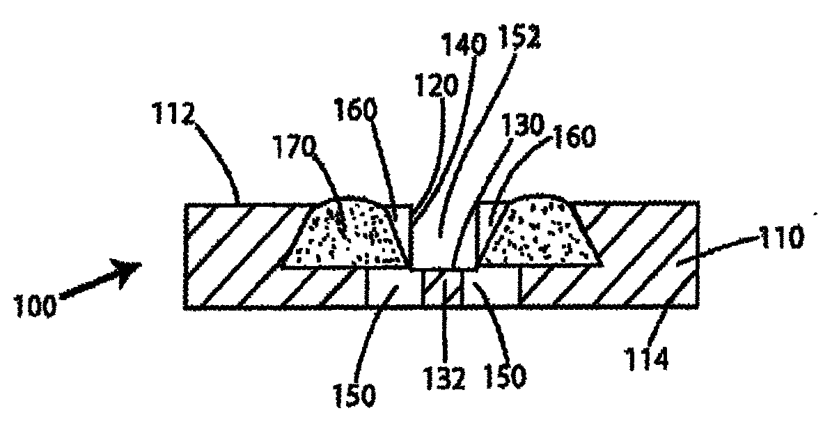
图1示出了由本体110构成的薄片或连接器壳体形式的连接器100。所述本体110可以具有任意不同的形状,在图示的实施方式中,所述本体110具有矩形形状。该本体110具有上表面112和相对的下表面114。FIG. 1 shows a connector 100 in the form of a wafer or connector housing formed by a body 110 . The body 110 may have any different shape, and in the illustrated embodiment, the body 110 has a rectangular shape. The body 110 has an upper surface 112 and an opposite lower surface 114 .

第一沟或槽120形成在上表面中,该槽120的底部由基底130限定。在图示的实施方式中,所述槽120还形成有两个间隔的垂直壁140(与所述基底130成直角)。A first trench or groove 120 is formed in the upper surface, the bottom of which groove 120 is defined by a base 130 . In the illustrated embodiment, the trough 120 is also formed with two spaced apart vertical walls 140 (at right angles to the base 130).

所述本体110还包括至少一个,且优选是多个第一回流开口或槽或通道150。每个回流槽150与所述基底130和下表面114连通。所述回流槽150可以是在所述槽120的内腔(室)152之间延伸的垂直槽的形式,并且还沿着所述下表面114构成了开口。The body 110 also includes at least one, and preferably a plurality of first return openings or slots or channels 150 . Each return channel 150 communicates with the base 130 and the lower surface 114 . The return channel 150 may be in the form of a vertical channel extending between lumens (chambers) 152 of the channel 120 and also forming an opening along the lower surface 114 .

当存在多个回流槽150时,这些槽150可以沿着所述基底130的侧边缘形成两排,其中所述垂直壁140横贯所述基底130,以便于所述基底130的中心部132保持在这些回流槽150之间来支撑物体(例如电子装置)。When there are multiple return channels 150, these channels 150 may form two rows along the side edges of the base 130, wherein the vertical wall 140 traverses the base 130, so that the central portion 132 of the base 130 remains in the Objects (such as electronic devices) are supported between the reflow tanks 150 .

所述本体110还包括至少一个,且优选是多个形成在限定所述沟或槽120的垂直壁140中的第二回流槽或开口160,以便于它们与所述槽120的内部连通。The body 110 also includes at least one, and preferably a plurality of, second return channels or openings 160 formed in the vertical wall 140 defining the trench or trough 120 so as to facilitate their communication with the interior of the trough 120 .

所述连接器100设计成容纳和保持至少一个,且优选地是多个焊料块(段)170。所述本体110包括多个形成在一平台182的相对两侧上的修整槽180(通孔),一个焊料段170位于所述平台上。形成所述修整槽180的制造原因在于比所需的焊料块170大的焊料块最初横跨两个间隔的修整槽180,并横跨所述平台182,然后冲压机或类似装置通过所述的两个间隔的修整槽180以便于将所述焊料块切割成仅保留在所述平台182上的一段170。The connector 100 is designed to receive and hold at least one, and preferably a plurality of solder bumps (segments) 170 . The body 110 includes a plurality of trim grooves 180 (through holes) formed on opposite sides of a platform 182 on which a solder segment 170 is located. The manufacturing reason for forming the trim slots 180 is that a solder bump larger than the desired solder bump 170 initially spans two spaced trim slots 180, and across the platform 182, and then a punch or similar device passes through the trim slots 180 as described. Two spaced apart trim grooves 180 facilitate cutting the solder bump into only a segment 170 remaining on the platform 182 .

根据所图示的实施方式,至少一个第一回流槽150和至少一个第二回流槽160与位于所述平台182上的焊料段170连通。换言之,第一回流槽150和第二回流槽160通向限定在所述平台182上方的空间。因此可以理解的是所述回流槽150,160是被专门定位的,以便于在回流时,(位于所述平台182上的)焊料段170回流并通过第一回流槽150和第二回流槽160,如图3中所示。According to the illustrated embodiment, at least one first reflow slot 150 and at least one second reflow slot 160 communicate with the solder segment 170 located on said platform 182 . In other words, the first return channel 150 and the second return channel 160 lead to the space defined above the platform 182 . Therefore, it can be understood that the reflow channels 150, 160 are specially positioned so that during reflow, the solder segment 170 (on the platform 182) reflows and passes through the first reflow channel 150 and the second reflow channel 160. , as shown in Figure 3.

如图3中所示,连接器100设计成将第一电子装置200电连接到第二电子装置300,且尤其是将第一电子装置200的接点或导电元件210电连接到第二电子装置300的接点或导电元件310上。As shown in FIG. 3 , the connector 100 is designed to electrically connect the first electronic device 200 to the second electronic device 300, and in particular to electrically connect the contacts or conductive elements 210 of the first electronic device 200 to the second electronic device 300. on the contact or conductive element 310.

第一电子装置200(例如子PCB)容纳在槽120中并被支撑在所述垂直壁140之间以便于保持竖直(垂直设计)。第二回流槽160形成在所述垂直壁140中以便于它们与第一电子装置200的接点(导电/可焊的焊点)210对齐。第一回流槽150形成为与第二电子装置300的接点310对齐。在所图示的实施方式中,第二电子装置300是相对于所述第一电子装置200(垂直PCB)水平定位的主PCB。A first electronic device 200 (eg, a sub PCB) is accommodated in the slot 120 and supported between the vertical walls 140 so as to be kept vertical (vertical design). Second reflow slots 160 are formed in the vertical walls 140 so that they align with the contacts (conductive/solderable pads) 210 of the first electronic device 200 . The first reflow tank 150 is formed to be aligned with the contact 310 of the second electronic device 300 . In the illustrated embodiment, the second electronic device 300 is a main PCB positioned horizontally relative to said first electronic device 200 (vertical PCB).

所述本体100由不可焊的材料形成,因此,在回流时,每个焊料段170回流以便于所述焊料被引导来将两个接点210,310弄湿。换言之,在焊料回流期间,所述焊料通过所述第一槽150回流并与所述接点310(主PCB)接触,同时通过所述第二槽160回流并与所述接点210(子PCB)接触。The body 100 is formed from a non-solderable material, therefore, upon reflow, each solder segment 170 reflows so that the solder is directed to wet the two joints 210, 310. In other words, during solder reflow, the solder reflows through the first slot 150 and contacts the joint 310 (main PCB), and at the same time reflows through the second slot 160 and contacts the joint 210 (sub PCB). .

在冷却时,在所述接点210与所述接点310之间形成了牢固的电连接。Upon cooling, a strong electrical connection is formed between the joints 210 and 310 .

图4-9示出了根据另一个实施方式的连接器400。该连接器400与连接器100类似的是其设计成将第一电子装置500(子PCB)电连接到第二电子装置600(主PCB)上,且尤其是其将第一电子装置500的接点或导电元件510电连接到第二电子装置600的接点或导电元件610上。4-9 illustrate a connector 400 according to another embodiment. The connector 400 is similar to the connector 100 in that it is designed to electrically connect the first electronic device 500 (sub-PCB) to the second electronic device 600 (main PCB), and in particular it connects the contacts of the first electronic device 500 Or the conductive element 510 is electrically connected to the contact or the conductive element 610 of the second electronic device 600 .

如这些图中所示,连接器400具有壳体410,该壳体410将焊料段700保持在垂直的方向上,如下所述,用于将第一电子装置500的一个接点510电连接到第二电子装置600的一个接点610上。所述壳体410实际上是由两部分构成的,这两部分相互接合并配合以构成如图1中所示的组装后的连接器400。特别地,所述壳体410由可选择性地相互配合的第一部件420和第二部件450构成。As shown in these figures, the connector 400 has a housing 410 that holds the solder segment 700 in a vertical orientation for electrically connecting a contact 510 of the first electronic device 500 to a second electronic device 500 as described below. On a contact 610 of the second electronic device 600 . The housing 410 is actually made up of two parts that engage and cooperate with each other to form the assembled connector 400 as shown in FIG. 1 . In particular, said housing 410 is composed of a first part 420 and a second part 450 which are selectively matable with each other.

第一和第二部件420,450可以由许多不同的材料形成,包括但不局限于多种不同的塑料。例如,第一和第二部件420,450可以形成为模制的塑料部件,可以理解的是所述连接器400(部件420,450)不形成为包括金属接点的印制接点构件。The first and second components 420, 450 may be formed from many different materials including, but not limited to, many different plastics. For example, the first and second parts 420, 450 may be formed as molded plastic parts, it being understood that the connector 400 (parts 420, 450) is not formed as a printed contact member including metal contacts.

第一部件420是细长的构件,其具有第一端422和相对的第二端424,以及顶面426和相对的底面428。第一部件420可以是至少部分地中空的构件。The first member 420 is an elongated member having a first end 422 and an opposing second end 424 , and a top surface 426 and an opposing bottom surface 428 . The first part 420 may be an at least partially hollow member.

在第一端422与第二端424之间,第一部件420包括多个焊料容纳构件430,每个焊料容纳构件430配置成容纳并保持焊料段700。每个焊料容纳构件430包括由一对相对的垂直侧壁432和一后垂直壁434限定的焊料容纳槽431。所述焊料容纳构件430彼此相互间隔从而导致所述焊料段700彼此相互间隔。如图6的顶视图中所看到的,所述焊料段700沿轴向定向,因为它们从一端422到另一端424沿着共用的轴线形成。Between the first end 422 and the second end 424 , the first component 420 includes a plurality of solder containment members 430 each configured to receive and retain a solder segment 700 . Each solder containment member 430 includes a solder containment channel 431 defined by a pair of opposing vertical side walls 432 and a rear vertical wall 434 . The solder receiving members 430 are spaced from each other causing the solder segments 700 to be spaced from each other. As seen in the top view of FIG. 6 , the solder segments 700 are axially oriented since they are formed along a common axis from one end 422 to the other end 424 .

所图示的每个焊料段700为示出具有药芯的细长焊料段的形式。每个焊料段700包括第一端702、相对的第二端704以及内表面706和面对其他部件420,450的相对的外表面708。当后垂直壁434是如图所示的平面时,焊料段700的内表面同样也会是平面。相对的外表面708可以如图所示的圆形的表面或者其可以是平面。类似地,侧壁432是平面,因此,焊料段700的侧面709同样可以是平面。Each solder segment 700 illustrated is in the form of an elongated solder segment shown with a flux core. Each solder segment 700 includes a first end 702 , an opposing second end 704 , and an inner surface 706 and an opposing outer surface 708 facing the other components 420 , 450 . While rear vertical wall 434 is planar as shown, the inner surface of solder segment 700 will also be planar. The opposing outer surface 708 may be a rounded surface as shown or it may be a planar surface. Similarly, sidewall 432 is planar, therefore, side 709 of solder segment 700 may also be planar.

可以理解的是焊料段700的尺寸和焊料容纳槽431的尺寸是彼此结合考虑而选择的以便于焊料段700被紧密地保持在所述焊料容纳槽431中。所述焊料容纳槽430相对于所述第一部件420是垂直定向的,因为它们沿上下的方向上延伸。焊料段700的深度可以大于焊料容纳构件430和焊料容纳槽431的深度,以便于焊料段700的内面或内表面702沿朝向第二部件450的方向突出所述焊料容纳构件430。It can be understood that the size of the solder segment 700 and the size of the solder receiving groove 431 are selected in consideration of each other so that the solder segment 700 is tightly held in the solder receiving groove 431 . The solder receiving grooves 430 are vertically oriented with respect to the first part 420 because they extend in an up and down direction. The depth of the solder segment 700 may be greater than the depth of the solder receiving member 430 and the solder receiving groove 431 such that the inner face or surface 702 of the solder segment 700 protrudes from the solder receiving member 430 in a direction toward the second component 450 .

端部422和424以及中间部425是第一部件420的组成部分,它们配置成与第二部件450的互补的部分配合来将第一和第二部件420、450彼此牢固地连接。为了将第一和第二部件420、450彼此连接,第一部件420可以包括多个固定元件,这些固定元件与第二部件450的互补的固定元件配合。例如,第一部件420可以包括多个自第一部件420的内部向外延伸的指状凸出部440。在所图示的实施方式中,第一部件420包括第一固定元件442,该第一固定元件442定位在第一部件420的第二端424附近或定位在第二端424上,并且自第一部件420的内部向外延伸。此外,所述中间部425包括第二固定元件444,该第二固定元件444自所述第一部件420的内部向外延伸。The end portions 422 and 424 and the intermediate portion 425 are integral parts of the first member 420 and are configured to cooperate with complementary portions of the second member 450 to securely connect the first and second members 420, 450 to each other. In order to connect the first and second parts 420 , 450 to each other, the first part 420 may comprise a plurality of fixing elements which cooperate with complementary fixing elements of the second part 450 . For example, the first member 420 may include a plurality of finger-shaped protrusions 440 extending outwardly from the interior of the first member 420 . In the illustrated embodiment, the first component 420 includes a first fixation element 442 positioned near or on the second end 424 of the first component 420 and extending from the second end 424. The interior of a part 420 extends outward. In addition, the middle portion 425 includes a second fixing element 444 extending outward from the inside of the first part 420 .

第一部件420的第一端422包括形成在其中的开口或槽427。该开口427包括互锁的部件,例如扣锁部件,其允许第二部件450的互补的凸出部(固定元件)与其相互锁定配合。The first end 422 of the first member 420 includes an opening or slot 427 formed therein. The opening 427 includes interlocking features, such as snap-lock features, which allow complementary projections (fixation elements) of the second part 450 to interlockingly engage therewith.

与第一部件420类似并互补的是,第二部件450是细长的构件,其具有第一端452和相对的第二端454以及顶面456和相对的底面458。第二部件450可以是至少部分地中空的构件。Similar to and complementary to first member 420 , second member 450 is an elongated member having a first end 452 and an opposing second end 454 and a top surface 456 and an opposing bottom surface 458 . The second component 450 may be an at least partially hollow member.

在第一端452与第二端454之间,第二部件450包括多个焊料容纳构件460,每个焊料容纳构件460配置成容纳并保持焊料段700。每个焊料容纳构件460包括由一对相对的垂直侧壁462和一后垂直壁464限定的焊料容纳槽461。所述焊料容纳构件460彼此相互间隔从而导致所述焊料段700彼此相互间隔。如图6的顶视图中所看到的,所述焊料段700沿轴向定向,因为它们从一端462到另一端464沿着共用的轴线形成。Between first end 452 and second end 454 , second component 450 includes a plurality of solder containment members 460 each configured to receive and retain a solder segment 700 . Each solder containment member 460 includes a solder containment channel 461 defined by a pair of opposing vertical side walls 462 and a rear vertical wall 464 . The solder receiving members 460 are spaced from each other causing the solder segments 700 to be spaced from each other. As seen in the top view of FIG. 6 , the solder segments 700 are axially oriented since they are formed along a common axis from one end 462 to the other end 464 .

当所述后垂直壁464是如图所示的平面时,所述焊料段700的内表面706同样会是平面。类似地,侧壁462是平面,因此所述焊料段700的侧面709同样可以是平面。While the rear vertical wall 464 is planar as shown, the inner surface 706 of the solder segment 700 will also be planar. Similarly, sidewall 462 is planar, so side 709 of solder segment 700 may also be planar.

可以理解的是焊料段700的尺寸和焊料容纳槽461的尺寸是相互结合考虑而选择的,以便于焊料段700被紧密地保持在所述焊料容纳槽461中。所述焊料容纳槽460相对于所述第二部件450是垂直定向的,因为它们沿上下的方向延伸。焊料段700的深度可以大于焊料容纳构件460和焊料容纳槽461的深度,以便于焊料段700的内面或内表面702沿朝向第一部件420的方向突出所述焊料容纳构件460。It can be understood that the size of the solder segment 700 and the size of the solder receiving groove 461 are selected in conjunction with each other so that the solder segment 700 is tightly held in the solder receiving groove 461 . The solder receiving grooves 460 are vertically oriented with respect to the second part 450 because they extend in an up and down direction. The depth of the solder segment 700 may be greater than the depth of the solder receiving member 460 and the solder receiving groove 461 such that the inner face or surface 702 of the solder segment 700 protrudes from the solder receiving member 460 in a direction toward the first component 420 .

端部462和464以及中间部455是第二部件450的组成部分,它们配置成与第一部件450的互补的部分配合来将第一和第二部件420,450彼此牢固地连接。为了将第一和第二部件420,450彼此连接,第二部件450可以包括许多固定元件,这些固定元件与第一部件420的互补的固定元件配合。例如,第二部件450可以包括多个自第二部件450的内部向外延伸的指状凸出部470。在所图示的实施方式中,第二部件450包括第一固定元件472,该第一固定元件472定位在第二部件450的第一端452附近或定位在第一端452上并且自第二部件450的内部向外延伸。此外,所述中间部455包括第二固定元件474,该第二固定元件474自所述第二部件450的内部向外延伸。The end portions 462 and 464 and the intermediate portion 455 are integral parts of the second member 450 and are configured to cooperate with complementary portions of the first member 450 to securely connect the first and second members 420, 450 to each other. In order to connect the first and second parts 420 , 450 to each other, the second part 450 may comprise a plurality of fixing elements which cooperate with complementary fixing elements of the first part 420 . For example, the second member 450 may include a plurality of finger-shaped protrusions 470 extending outwardly from the interior of the second member 450 . In the illustrated embodiment, the second member 450 includes a first fixation element 472 positioned near or on the first end 452 of the second member 450 and extending from the second end 452 . The interior of member 450 extends outward. Furthermore, the intermediate portion 455 includes a second fixing element 474 extending outwardly from the interior of the second part 450 .

第二部件450的第二端454包括形成在其中的开口或槽457。该开口457包括互锁的部件,例如扣锁部件,其允许第一部件420的互补的凸出部(这种情况下是第一固定元件442)与其相互锁定配合。例如,当两个部件420、450配合在一起时,凸出部442容纳在开口457中,凸出部444容纳在形成在中间部455中的开口469中,凸出部474容纳在中间部425中的开口429中,且凸出部472容纳在开口427中。正如先前提到的,两个部件420、450可以相互卡扣配合,或者可以使用另一种类型的固定配置。The second end 454 of the second member 450 includes an opening or slot 457 formed therein. The opening 457 includes interlocking features, such as snap-lock features, which allow a complementary projection of the first part 420 , in this case the first securing element 442 , to interlockingly engage therewith. For example, when the two parts 420, 450 are mated together, the protrusion 442 is received in the opening 457, the protrusion 444 is received in the opening 469 formed in the intermediate portion 455, and the protrusion 474 is received in the intermediate portion 425. In the opening 429 in, and the protrusion 472 is received in the opening 427. As previously mentioned, the two parts 420, 450 may be snap-fitted to each other, or another type of securing arrangement may be used.

从绘制的图中可以理解的是,当两个部件420、450配合在一起时,保持在第一部件420的焊料容纳构件430中的焊料段700从保持在第二部件450的焊料容纳构件460中的焊料段700越过并与其对齐。更具体地说,固定元件的互补对配合在一起来使第一和第二部件420、450连接并且所述焊料段700适当地对齐,以便于配合的、相对的焊料段700对被限定并被适当地定位以便于将第一电子装置500电连接到第二电子装置600上。It can be understood from the drawn figures that when the two parts 420, 450 are mated together, the solder segment 700 held in the solder receiving member 430 of the first part 420 is released from the solder receiving member 460 held in the second part 450. The solder segment 700 in the cross and aligned with it. More specifically, complementary pairs of fixation elements fit together to connect the first and second components 420, 450 and the solder segments 700 are properly aligned so that mating, opposing pairs of solder segments 700 are defined and defined. Suitably positioned to facilitate electrical connection of the first electronic device 500 to the second electronic device 600 .

为了将两个部件420、450彼此连接,可以使用任何数量的不同类型的固定元件。In order to connect the two parts 420, 450 to each other, any number of different types of fixing elements may be used.

还可以理解的是用于将第一和第二部件420、450彼此连接的固定元件可以是可脱开型的,因此,第一和第二部件420、450在某些情况下可以重新使用。在其他的实施方式中,第一与第二部件420、450之间的更持久的连接可以通过卡扣连接等来提供,其中一旦两个部件420、450被彼此锁住,它们不能被轻易地分开。正如这些图中所示的,这两个部件420、450不仅在它们的端部连接,而且在中间部上也连接。It is also understood that the securing elements used to connect the first and second parts 420, 450 to each other may be of the releasable type, so that the first and second parts 420, 450 may be reused in some cases. In other embodiments, a more permanent connection between the first and second parts 420, 450 may be provided by a snap connection or the like, wherein once the two parts 420, 450 are locked to each other, they cannot be easily removed. separate. As shown in these figures, the two parts 420, 450 are connected not only at their ends, but also in the middle.

当然,第一和第二部件420、450起初彼此分开,以允许容易地将焊料段装入各自的焊料容纳构件中。例如,可以设置自动系统来将长的焊料段分割成具有合适尺寸和形状的单个的焊料段700,然后该机器可以将所述的单个的焊料段700放置在它们各自的焊料容纳构件中。特别地,自动活塞或拨爪能够可控制地接触并引导所述单个的焊料段进入一个焊料容纳构件中。正如先前提到的,所述焊料段700可以靠摩擦保持在限定所述焊料容纳构件的壁表面之间。Of course, the first and second components 420, 450 are initially separated from each other to allow easy loading of the solder segments into the respective solder containing members. For example, an automated system may be provided to divide long solder segments into individual solder segments 700 of suitable size and shape, which machines may then place said individual solder segments 700 in their respective solder containment members. In particular, automatic pistons or fingers are capable of controllably contacting and guiding the individual solder segments into a solder containing member. As previously mentioned, the solder segment 700 may be frictionally retained between the wall surfaces defining the solder containment member.

在该特殊实施方式中,所述焊料段700被垂直地保持在第一和第二部件420、450的焊料容纳构件中。因为焊料段700以相对的对向对的形式布置,所以它们限定了多个用于将第一电子装置500电连接到第二电子装置600上的焊点。In this particular embodiment, the solder segment 700 is held vertically in the solder containing members of the first and second components 420 , 450 . Because the solder segments 700 are arranged in opposing facing pairs, they define a plurality of solder joints for electrically connecting the first electronic device 500 to the second electronic device 600 .

如图7中所示还可以理解的是,当第一和第二部件420、450配合在一起时,在焊料段700的彼此面对隔开的外表面708之间形成了间隙空间800。该空间800设计成容纳一构件以便于该构件被布置成与第一和第二部件420、450的焊料段700紧密接触。在图示的实施方式中,该间隙800一般形成为矩形。此外,在任意相对的焊料段700对之间的间隙或空间800应该是相同的。换言之,在每个相对的焊料段700对之间应该存在相同的距离,因为在它们之间形成的间隙被设计成容纳一般具有均匀厚度的第一电子装置500。当第一电子装置500被容纳在所述间隙800中时,因为该第一电子装置500竖立在所述间隙800中,所以该第一电子装置500与和第一和第二部件420、450相连的每个焊料段700紧密接触。It will also be appreciated that, as shown in FIG. 7 , when the first and second components 420 , 450 are mated together, an interstitial space 800 is formed between the facing and spaced outer surfaces 708 of the solder segment 700 . The space 800 is designed to accommodate a component such that the component is arranged in intimate contact with the solder segment 700 of the first and second components 420 , 450 . In the illustrated embodiment, the gap 800 is generally formed as a rectangle. Furthermore, the gap or space 800 between any opposing pair of solder segments 700 should be the same. In other words, there should be the same distance between each pair of opposing solder segments 700, since the gap formed between them is designed to accommodate the first electronic device 500, which generally has a uniform thickness. When the first electronic device 500 is accommodated in the gap 800, since the first electronic device 500 stands in the gap 800, the first electronic device 500 is connected with the first and second components 420, 450 Each solder segment 700 is in close contact.

两个部件420、450的中间部将所述间隙800分成两个不同的部分,且特别地,在两个部件420、450的中间部与第一端之间形成有第一间隙800,且在两个部件420、450的中间部与第二端之间形成有第二间隙800。此外,虽然图示的实施方式示出了第一和第二部件420、450中的每一个包括两组十焊料段700,但是可以理解的是这些数量的焊料段700仅是为了图示的目的,每个部件420、450可以载有多于或少于该数量的焊料段。因此,一组焊料段可以在数量上多于另一组焊料段。The middle part of the two parts 420, 450 divides said gap 800 into two different parts, and in particular, a first gap 800 is formed between the middle part and the first end of the two parts 420, 450, and at A second gap 800 is formed between the middle portion and the second end of the two parts 420 , 450 . Furthermore, while the illustrated embodiment shows that each of the first and second components 420, 450 includes two sets of ten solder segments 700, it is to be understood that these numbers of solder segments 700 are for illustration purposes only. , each component 420, 450 may carry more or less than this number of solder segments. Thus, one set of solder segments may be greater in number than another set of solder segments.

现在将参照附图来描述组装和使用连接器400的方法。正如先前提到的,第一电子装置500是具有下边缘502的基片(如,印刷电路板)的形式。沿着所述下边缘502,第一电子装置500具有多个接点510,这些接点510可以是沿着所述下边缘502间隔开选定间隔的导电焊点的形式。在图示的实施方式中,导电焊点510具有矩形形状;但是,这些焊点510可以具有其他任何的形状,包括正方形、椭圆形、圆形,等等。可以理解的是,第一电子装置500是垂直安装式的印刷电路板等,因为其在安装到第二电子装置600上时是垂直竖立的。第一电子装置500还具有相对的垂直面,因为其包括第一垂直面520和相对的第二垂直面530。导电接点510沿着第一垂直面520和第二垂直面530中的每一个的下边缘502布置。以这种方式,导电焊点510被定位在彼此相对的两侧上;但是,它们位于各自的垂直面520,530的相同的位置中。此外,导电焊点510在一个面520上的间距优选地与在另一个面530上的间距是相同的。Methods of assembling and using the connector 400 will now be described with reference to the accompanying drawings. As previously mentioned, the first electronic device 500 is in the form of a substrate (eg, a printed circuit board) having a lower edge 502 . Along the lower edge 502 , the first electronic device 500 has a plurality of contacts 510 which may be in the form of conductive pads spaced at selected intervals along the lower edge 502 . In the illustrated embodiment, the conductive pads 510 have a rectangular shape; however, these pads 510 may have any other shape, including square, oval, circular, and the like. It can be understood that the first electronic device 500 is a vertically mounted printed circuit board or the like, because it stands vertically when mounted on the second electronic device 600 . The first electronic device 500 also has opposite vertical faces because it includes a first vertical face 520 and an opposite second vertical face 530 . The conductive contacts 510 are arranged along the lower edge 502 of each of the first vertical surface 520 and the second vertical surface 530 . In this way, the conductive pads 510 are positioned on opposite sides of each other; however, they are located in the same position on the respective vertical planes 520,530. Furthermore, the spacing of the conductive pads 510 on one side 520 is preferably the same as the spacing on the other side 530 .

为了容下第一和第二部件420、450的中间部425、455,第一电子装置500包括容纳两个部件420、450的固定元件的切口550。在图示的实施方式中,所述切口550具有半圆形的形状;但是,其并不局限于具有这样的形状,其可以具有其他任何形状,包括但不局限于正方形,等等,只要该切口550允许所述固定元件从其中通过并且允许第一电子装置容纳在中间部各侧上的两个间隙800中,以使第一电子装置500贴合地安装在第二电子装置600上,正如下面所描述的那样。In order to accommodate the intermediate portions 425 , 455 of the first and second parts 420 , 450 , the first electronic device 500 includes cutouts 550 for receiving the fixing elements of the two parts 420 , 450 . In the illustrated embodiment, the cutout 550 has a semicircular shape; however, it is not limited to having such a shape, and it may have any other shape, including but not limited to a square, etc., as long as the The cutouts 550 allow passage of the fixing elements therethrough and allow the first electronic device to be accommodated in the two gaps 800 on each side of the middle portion so that the first electronic device 500 is snugly mounted on the second electronic device 600, as as described below.

因此第二电子装置600是一种水平式的装置,其包括顶面602。该顶面602是含有接点610的那个表面,特别地,所述接点610布置成两排间隔开的接点。例如,接点610在轴向上布置成接点610的第一排613和接点610的第二排615,在它们之间具有空间620。该空间620具有基本为矩形的形状。Therefore, the second electronic device 600 is a horizontal device, which includes a top surface 602 . The top surface 602 is that surface containing the contacts 610, in particular said contacts 610 arranged in two rows of spaced apart contacts. For example, the contacts 610 are axially arranged in a first row 613 of contacts 610 and a second row 615 of contacts 610 with a space 620 therebetween. The space 620 has a substantially rectangular shape.

在图示的实施方式中,接点610具有正方形或矩形的形状;但是,再次重申,接点610并不局限于这些形状,其可以具有任何不同的形状。In the illustrated embodiment, the contacts 610 have a square or rectangular shape; however, again, the contacts 610 are not limited to these shapes and may have any different shape.

接点510的数量一般等于接点610的数量,以便于对于每个接点510来说存在相对于其合适定位的对应的接点610。两排接点610之间的间距大约等于第一电子装置500的厚度,因此在这两排之间形成了没有任何导电材料的区域620。第一电子装置500的底边缘503位于该区域620内。The number of contacts 510 is generally equal to the number of contacts 610 so that for each contact 510 there is a corresponding contact 610 properly positioned relative thereto. The distance between the two rows of contacts 610 is approximately equal to the thickness of the first electronic device 500, thus forming a region 620 without any conductive material between the two rows. The bottom edge 503 of the first electronic device 500 is located within the area 620 .

接点610之间的间距应该约等于接点510之间的间距,以便于在第一和第二电子装置500,600关于彼此布置时,排613中的每个接点610具有沿着第一垂直面520的下边缘502形成的对应的接点510。类似地,排615中的每个接点610具有沿着第二垂直面530的下边缘502形成的对应的接点510。The spacing between the contacts 610 should be approximately equal to the spacing between the contacts 510 so that when the first and second electronic devices 500, 600 are arranged with respect to each other, each contact 610 in the row 613 has an The corresponding contacts 510 are formed by the lower edge 502 of the . Similarly, each contact 610 in row 615 has a corresponding contact 510 formed along lower edge 502 of second vertical face 530 .

因为第一电子装置500垂直于第二电子装置600安装,所以对应的接点对510、610同样彼此垂直定位,如图所示。Because the first electronic device 500 is mounted perpendicular to the second electronic device 600, the corresponding contact pairs 510, 610 are also positioned perpendicular to each other, as shown.

为了恰当地定位第一和第二电子装置500、600,第一电子装置500被定位以便于排613中的接点610紧接沿着第一垂直面520的边缘502的接点510定位,类似地,排615中的接点610紧接沿着第二垂直面530的边缘502的接点510定位。更具体地说,在每个接点610与对应的接点510之间形成直角。In order to properly position the first and second electronic devices 500, 600, the first electronic device 500 is positioned so that the contacts 610 in the row 613 are positioned next to the contacts 510 along the edge 502 of the first vertical plane 520, similarly, The contacts 610 in the row 615 are located next to the contacts 510 along the edge 502 of the second vertical face 530 . More specifically, a right angle is formed between each joint 610 and the corresponding joint 510 .

为了将第一电子装置500电连接到第二电子装置600上,连接器400的其中一个部件420、450相对于垂直定向的第一电子装置500定位。例如如图5中所示,第一部件420相对于第一电子装置500定位以便于保持在第一部件420的焊料容纳构件中的焊料段700既面对接点510又面对接点610。在每个端部422、424附近,第一部件包括一对端壁423,该对端壁423限定了间隙800的端部,并且还作为定位器和止动件来在组装所述连接器400时限制第一电子装置500在所述间隙800内的运动。第一电子装置500因此布置在这些端壁423之间。所述端壁423还限定了彼此紧固以连接到第一和第二部件420、450上的端部件的起点。可以从图中看出,这些端部件具有内壁,在第一和第二部件420、450被连接以形成组装后的连接器400时,这些内壁布置成彼此紧密接触。In order to electrically connect the first electronic device 500 to the second electronic device 600 , one of the components 420 , 450 of the connector 400 is positioned relative to the vertically oriented first electronic device 500 . For example, as shown in FIG. 5 , first component 420 is positioned relative to first electronic device 500 such that solder segment 700 held in the solder-receiving member of first component 420 faces both joint 510 and joint 610 . Near each end 422, 424, the first part includes a pair of end walls 423 that define the ends of the gap 800 and also serve as locators and stops when assembling the connector 400. The movement of the first electronic device 500 in the gap 800 is restricted at the same time. The first electronic device 500 is thus arranged between these end walls 423 . Said end wall 423 also defines the origin of the end pieces fastened to each other for connection to the first and second pieces 420 , 450 . As can be seen from the figure, these end pieces have inner walls which are arranged in intimate contact with each other when the first and second pieces 420 , 450 are connected to form the assembled connector 400 .

第一部件420布置在第二电子装置600的顶面之上,并且被定位以便于所述焊料段700被布置在接点610上方,同时,焊料段700的外表面708被紧接第一电子装置500的垂直定向的接点510设置或者被设置成与所述接点510紧密接触。因此,对于每一对接点510、610,存在一个焊料段700,也就是该焊料段700在回流时将接点510、610彼此电连接,正如下面所述。The first component 420 is disposed on the top surface of the second electronic device 600 and is positioned so that the solder segment 700 is disposed above the joint 610 while the outer surface 708 of the solder segment 700 is positioned in close proximity to the first electronic device. The vertically oriented joint 510 of 500 is disposed or arranged in intimate contact with said joint 510 . Thus, for each butt joint 510, 610, there is one solder segment 700, ie, the solder segment 700 electrically connects the joints 510, 610 to each other during reflow, as described below.

凸出部444、474穿过切口550而被容纳以允许它们与对应的开口469、429配合,并且固定元件442、472位于第一和第二部件420、450的位于焊料段700和第一电子装置500所处的位置之外的端部件中。这些端部件和固定元件442、472因此约束并围绕第一电子装置500的端部。可以理解的是,当第一和第二部件420、450彼此配合时,对应的固定元件在视图中被隐藏了,因为这些部件420、450的内表面彼此平齐固定。Projections 444, 474 are received through cutouts 550 to allow them to mate with corresponding openings 469, 429, and securing elements 442, 472 are located between solder segments 700 and first electronics of first and second components 420, 450. In an end piece other than where the device 500 is located. These end pieces and fixing elements 442 , 472 thus constrain and surround the ends of the first electronic device 500 . It will be appreciated that when the first and second parts 420, 450 are mated to each other, the corresponding securing elements are hidden from view, since the inner surfaces of these parts 420, 450 are secured flush with each other.

当第一和第二部件420、450的固定元件彼此配合时,这两个部件420、450彼此牢固地连接,其中第一电子装置500容纳在间隙800中,并且焊料段700被合适地定位以便于每个焊料段700被布置在一个接点610的上方并靠近一个接点510。When the fixing elements of the first and second parts 420, 450 cooperate with each other, the two parts 420, 450 are firmly connected to each other, with the first electronic device 500 accommodated in the gap 800, and the solder segment 700 is properly positioned so that Each solder segment 700 is disposed above a joint 610 and close to a joint 510 .

要将第一和第二电子装置500、600彼此电连接,使用传统的技术将连接器400和焊料段700加热以使焊料段700回流。图9示出了处于回流状态的焊料段700,特别地,当每个焊料段700回流时,所述焊料段流动与接点610和接点510接触,停止加热时焊料段在该区域内凝固。以这种方式,焊料段700在接点610与接点510之间提供了电连接。焊料段700的回流发生在焊料槽431、461中。可以看出这些槽431、461在连接器400放置在连接器400上方时覆盖在接点610上面。To electrically connect the first and second electronic devices 500, 600 to each other, the connector 400 and the solder segment 700 are heated to reflow the solder segment 700 using conventional techniques. Figure 9 shows the solder segments 700 in a reflow state, in particular, as each solder segment 700 reflows, the solder segments flow into contact with joints 610 and 510, and the solder segments solidify in this area when heating is stopped. In this manner, solder segment 700 provides an electrical connection between joint 610 and joint 510 . The reflow of the solder segment 700 takes place in the solder baths 431 , 461 . It can be seen that these slots 431 , 461 overlie the contacts 610 when the connector 400 is placed over the connector 400 .

可选地,第一和第二部件420、450可以早已彼此连接,其中焊料段700牢固地附带其中。在这种情况下,第一电子装置500的下边缘502仅插入到间隙800中,然后第一电子装置500和连接器400相对于第二电子装置500定位,以便于焊料段700设置在接点610上方。在该实施方式中,连接器400的尺寸专门设计以容纳某种类型(例如厚度)的第一电子装置500。可以为不同尺寸(例如不同厚度)的子插板(第一电子装置500)来提供不同的连接器400。Alternatively, the first and second components 420, 450 may already be connected to each other with the solder segment 700 securely attached thereto. In this case, the lower edge 502 of the first electronic device 500 is only inserted into the gap 800, and then the first electronic device 500 and the connector 400 are positioned relative to the second electronic device 500 so that the solder segment 700 is disposed on the joint 610 above. In this embodiment, the size of the connector 400 is specially designed to accommodate a certain type (eg thickness) of the first electronic device 500 . Different connectors 400 may be provided for daughterboards (first electronic device 500 ) of different sizes (eg, different thicknesses).

还可以理解的是,本发明的连接器被构造成允许消费者将两个分离的连接件,即部件420、450以适合于各种尺寸(例如不同厚度)的大量子插板(第一电子装置500)的方式压配在一起。It will also be appreciated that the connector of the present invention is configured to allow the consumer to adapt two separate connectors, i.e. parts 420, 450, to fit various sizes (e.g. different thicknesses) of Quantum Boards (first electronic device 500) are press-fitted together.

在图4-9的实施方式中,焊料段700通过具有鸽子尾巴形状的焊料变形体来保持在各自的连接器部件420、450中。在图10中,焊料段700被处理以便于提高保持力,更具体地说,将一工具压向焊料段700的外表面708以形成下凹的或凹入的部分709。凹入的部分709的形成有助于更好地驱动焊料段700进入焊料容纳构件的鸽子尾巴形状的角落。所述工具可以是自动系统的部分,在这种情况下在一个自动构件将焊料段700放置在焊料容纳构件中之后,另一个自动构件接触焊料段700并将焊料段700压入鸽子尾巴形状的构件的角落,从而形成了凹入的部分709。图示的凹入的部分709具有三角形或V形的形状。In the embodiment of Figures 4-9, the solder segment 700 is retained in the respective connector part 420, 450 by a solder deformation having a dove tail shape. In FIG. 10 , the solder segment 700 is processed to facilitate retention, more specifically, a tool is pressed against the outer surface 708 of the solder segment 700 to form a depressed or concave portion 709 . The formation of the concave portion 709 helps to better drive the solder segment 700 into the dove tail shaped corner of the solder receiving member. The tool may be part of an automated system, in which case after one automated component places the solder segment 700 in the solder containing component, another automated component contacts the solder segment 700 and presses the solder segment 700 into a dove tail shaped corners of the member, thereby forming a recessed portion 709 . The illustrated concave portion 709 has a triangular or V-shape.

图11A和B示出了另一种用于提高焊料保持构件的所述槽中的焊料保持力的装置。在该实施方式中,焊料保持装置770形成在焊料保持槽中。该焊料保持装置770可以是自所述后壁464向外延伸的台阶、短小突出部或隆起的形式。在一个实施方式中,台阶770位于所述槽的中间(例如既在垂直方向上又在横向上)。台阶770设计成限制焊料段700在焊料保持槽中的轴向运动。Figures 11A and B illustrate another means for improving solder retention in the grooves of the solder retention member. In this embodiment, the solder retaining means 770 is formed in the solder retaining groove. The solder retaining means 770 may be in the form of a step, tab or bump extending outwardly from the rear wall 464 . In one embodiment, the step 770 is located in the middle of the slot (eg, both vertically and laterally). The step 770 is designed to limit the axial movement of the solder segment 700 in the solder holding groove.

换言之,焊料保持装置770提高了连接器400中的焊料轴向保持力,因为焊料段400插入到焊料槽中导致了所述装置770被压入到了焊料段700的本体中,如图11B中所示。所述装置770插入到焊料段700的本体中限制了焊料段700在焊料槽中的上下(垂直轴)运动,因为该装置770用来将焊料段700保持在所述槽中的适当位置。所述装置770的精确的形状不是关键的。在图示的实施方式中,该装置770具有圆形的毛边(freeedge),并且具有类似于吉他拨片的形状;但是,这只是一种示例性形状。In other words, the solder retention device 770 improves the axial retention of the solder in the connector 400 because the insertion of the solder segment 400 into the solder bath causes the device 770 to be pressed into the body of the solder segment 700, as shown in FIG. 11B Show. Insertion of the device 770 into the body of the solder segment 700 limits the up and down (vertical axis) movement of the solder segment 700 in the solder bath, as the device 770 serves to hold the solder segment 700 in place in the bath. The precise shape of the device 770 is not critical. In the illustrated embodiment, the device 770 has a rounded freeedge and has a shape similar to a guitar pick; however, this is only an exemplary shape.

台阶770优选地不向外超出焊料保持构件430、460的侧壁432、462(图6)。台阶770可以是第一和第二连接器部件420、450的整体的一部分,正如在普通的模制过程中形成所述台阶770的情况那样。The step 770 preferably does not extend outward beyond the sidewalls 432, 462 of the solder retaining members 430, 460 (FIG. 6). The step 770 may be an integral part of the first and second connector components 420, 450, as would be the case in forming the step 770 during a conventional molding process.

虽然出于解释的目的已经披露了优选的实施方式,但是本领域的技术人员可以理解,在不脱离本发明的范围和精髓的情况下许多添加、修改和置换是可行的。Although a preferred embodiment has been disclosed for purposes of illustration, those skilled in the art will appreciate that many additions, modifications and substitutions are possible without departing from the scope and spirit of the invention.

Claims (27)

1. electric connector that is used for first electronic circuit is electrically connected to second electronic circuit, described first electronic circuit has at least one first contact on its one side, described second electronic circuit has at least one second contact on its one side, this connector comprises:
Housing, this housing comprises:
At least one scolder keeps groove, and described scolder keeps groove to be configured to solder segment is remained on wherein, and
Slit, contiguous described scolder keeps groove to form, and be configured to along holding first electronic circuit perpendicular to the vertical substantially direction of second electronic circuit, make the contiguous described scolder of described at least one first contact on described that is formed on described first electronic circuit keep groove to arrange, and at least a portion of described at least one second contact that forms along the one side of described second electronic circuit is arranged in the below that described scolder keeps groove.
2. electric connector according to claim 1 also comprises the solder segment that is arranged in the described scolder maintenance groove.
3. electric connector according to claim 2, wherein said solder segment have outside vertical orientation makes that the vertical surface of described at least solder segment and bottom are exposed to.
4. electric connector that is used for first electronic circuit is electrically connected to second electronic circuit comprises:
Housing, this housing comprise that a plurality of scolders keep groove, and each scolder keeps groove to be configured to keep solder segment, and described scolder keeps flute profile to become the first relative row and second row, is formed with unlimited space between described first row and second row.
5. electric connector according to claim 4 also comprises the solder segment that is arranged in each scolder maintenance groove.
6. electric connector according to claim 5, wherein each solder segment has outside vertical orientation makes that the vertical surface of described at least solder segment and bottom are exposed to, and
Corresponding solder segment among the wherein relative row be exposed to outer vertical surface toward each other.
7. electric connector according to claim 6 is outside the top of wherein said solder segment is exposed to.
8. electric connector according to claim 5, wherein each groove is limited by an a pair of relative sidewall and a rear wall, and described solder segment frictionally remains in the described groove between the described sidewall.
9. electric connector according to claim 4, wherein said housing is made of first parts and second parts, and first parts comprise that first row's scolder keeps groove, and second parts comprise that second row's scolder keeps groove.
10. electric connector according to claim 9, first wherein relative row and the described unlimited spatial configuration between second row become to hold first electronic circuit, make the scolder of the contiguous respective row of lip-deep first contact of the opposing vertical that is formed on first electronic circuit keep groove to arrange.
11. electric connector according to claim 10, wherein said unlimited space are the forms of slit, it is configured to hold first electronic circuit makes the electronic circuit of winning be erected in the described slit in vertical mode.
12. electric connector according to claim 11 also comprises the solder segment that is arranged in each scolder maintenance groove, and
Wherein the degree of depth of each solder segment makes described solder segment extend beyond the sidewall that scolder keeps groove, and makes described solder segment limit described slit greater than the degree of depth of corresponding scolder maintenance groove.
13. electric connector according to claim 9, but wherein first parts and second parts each other buckle be connected.
14. electric connector according to claim 9, wherein first parts and second parts they relative two ends and pars intermedia on be connected to each other, each corresponding pars intermedia keeps groove to be divided into two different parts in corresponding every row's scolder.
15. connector according to claim 4, wherein said scolder keep groove to comprise the scolder holding element that is formed on wherein, this scolder holding element is configured to limit the axial motion that is arranged in the solder segment in the described groove.
16. connector according to claim 15, wherein said scolder holding element comprises protuberance, and this protuberance reaches in the described scolder maintenance groove and is bonded in the solder segment, with restrictive axial motion in vertical direction.
17. connector according to claim 16 wherein roughly is formed in the pars intermedia of described groove at described protuberance when the vertical axis of described groove is measured.
18. connector according to claim 4, wherein said housing are formed by plastics and do not have a hardware.
19. an electric connector that is used for first electronic circuit is electrically connected to second electronic circuit comprises:
Housing with upper surface and lower surface, this housing comprises:
Groove is arranged in the described upper surface, and has two isolated vertical walls, and described vertical wall is configured to keep therein described first electronic circuit,
At least one backflash that is communicated with described groove and lower surface, and
Be configured to keep at least one platform of at least one solder bump, it is electrically connected second electronic circuit of first electronic circuit below being arranged in described lower surface by described backflash after refluxing.
20. electric connector according to claim 19 also comprises at least one solder bump that contiguous described backflash is arranged.
21. electric connector according to claim 20 also comprises at least one trim slots that contiguous described platform is arranged.
22. a method that is used for first electronic circuit is electrically connected to second electronic circuit comprises:
A connector is provided, this connector comprises housing, described housing has a plurality of scolders and keeps groove, described a plurality of scolder keeps groove that a plurality of solder segment are remained on wherein, outside wherein the vertical surface of each solder segment and an end are exposed at least, described scolder keeps flute profile to become the first relative row and second row, is formed with unlimited space between described first row and second row;
Described connector is placed on the face of second electronic circuit, described second electronic circuit on this face, have be spaced apart from each other two ranked second contact, described connector be placed to make described at least a portion that is exposed to outer end of solder segment row be arranged in the top of second bank of contacts;
With first electrical circuit arrangement in described unlimited space, make it vertically locate with respect to the described connector and second electronic circuit, described first electronic circuit first ranked first contact what have solder segment location in contiguous first emissions groove on the face, and has second of solder segment location in contiguous second emissions groove ranked first contact on relative face; And
Described solder segment is back to respectively on first contact and second contact, thereby corresponding first contact of first electronic circuit is electrically connected on corresponding second contact of second electronic circuit.
23. method according to claim 22 also comprises:
Utilize instrument that described solder segment is pressed in the described groove, thereby form recessed feature, and cause described solder segment to be directed in the corner of described groove.
24. method according to claim 22 also comprises:
Limit described solder segment axial motion in vertical direction in the described groove by forming protuberance, wherein said protuberance stretches in the described groove and with described solder segment and is inserted in the described groove, thereby causes described protuberance to be embedded in the described solder segment.
25. method according to claim 22, wherein said first electronic circuit are the daughter boards of vertical orientation, and described second electronic circuit is the mainboard of the horizontal orientation vertical with described first electronic circuit.
26. a method that is used for first electronic circuit is electrically connected to second electronic circuit comprises:
A connector is provided, this connector comprises housing, and described housing has upper surface and lower surface, be arranged in the described upper surface and have the groove of two isolated vertical walls, at least one backflash that is communicated with described groove and described lower surface and at least one contiguous described backflash and be configured to keep the platform of at least one solder segment;
Described connector is placed on the face of second electronic circuit, described second electronic circuit comprises at least one second contact on this face, described connector is placed to make described backflash be disposed in the top of at least a portion of described second contact;
In described groove, make it with respect to the described connector and the second electronic circuit perpendicular positioning first electrical circuit arrangement, described first electronic circuit has at least one first contact of contiguous described backflash on one face; And
Described solder segment is back on first contact and second contact by described backflash, thereby first contact of first electronic circuit is electrically connected on second contact of second electronic circuit.
27. method according to claim 26 also comprises:
Described solder segment is arranged on the described platform of described housing;
Cut and be right after the trim slots that described platform is arranged, so that cut described solder segment.
CN2008800137384A 2007-04-26 2008-04-25 Electrical connector and method for electrically connecting first electronic device to second electronic device Active CN101682126B (en)

Applications Claiming Priority (5)

Application Number Priority Date Filing Date Title
US91425507P 2007-04-26 2007-04-26
US60/914,255 2007-04-26
US12/038,635 US7758350B2 (en) 2007-04-26 2008-02-27 Electrical connector with solder retention means for assembly
US12/038,635 2008-02-27
PCT/US2008/061555 WO2008134501A1 (en) 2007-04-26 2008-04-25 Electrical connector for use in soldering operations

Publications (2)

Publication Number Publication Date
CN101682126A true CN101682126A (en) 2010-03-24
CN101682126B CN101682126B (en) 2011-11-30

Family

ID=39887513

Family Applications (1)

Application Number Title Priority Date Filing Date
CN2008800137384A Active CN101682126B (en) 2007-04-26 2008-04-25 Electrical connector and method for electrically connecting first electronic device to second electronic device

Country Status (5)

Country Link
US (1) US7758350B2 (en)
EP (1) EP2176925A4 (en)
CN (1) CN101682126B (en)
TW (1) TWI410010B (en)
WO (1) WO2008134501A1 (en)

Cited By (2)

* Cited by examiner, † Cited by third party
Publication number Priority date Publication date Assignee Title
CN108493629A (en) * 2018-03-12 2018-09-04 福耀集团(上海)汽车玻璃有限公司 A kind of electrical coupling element and vehicle glass
CN108695602A (en) * 2017-03-29 2018-10-23 泰连德国有限公司 Electrical contact member and the indentation welding body made of hard solder form the method for welding conductive connection part to the hard solder of cooperation contact

Families Citing this family (2)

* Cited by examiner, † Cited by third party
Publication number Priority date Publication date Assignee Title
JP2016152083A (en) * 2015-02-16 2016-08-22 タイコエレクトロニクスジャパン合同会社 Connector
CN106363312B (en) * 2016-11-23 2019-03-08 京信通信技术(广州)有限公司 Weld matrix

Family Cites Families (11)

* Cited by examiner, † Cited by third party
Publication number Priority date Publication date Assignee Title
US5139448A (en) * 1985-05-24 1992-08-18 North American Specialties Corporation Solder-bearing lead
US4985990A (en) * 1988-12-14 1991-01-22 International Business Machines Corporation Method of forming conductors within an insulating substrate
US4900279A (en) * 1989-04-24 1990-02-13 Die Tech, Inc. Solder terminal
KR100339767B1 (en) * 1993-12-09 2002-11-30 메소드 일렉트로닉스 인코포레이티드 Electrical connector for electric signal transmission and its manufacturing method
US6543129B2 (en) 1995-11-03 2003-04-08 Teka Interconnections Systems, Inc. Solder-bearing contacts and method of manufacture thereof and use in a solder ball grid array connector
US6089920A (en) * 1998-05-04 2000-07-18 Micron Technology, Inc. Modular die sockets with flexible interconnects for packaging bare semiconductor die
WO2000067346A1 (en) * 1999-04-30 2000-11-09 Die Tech, Inc. Edge clip terminal and method
DE10057460C1 (en) * 2000-11-20 2002-08-08 Tyco Electronics Amp Gmbh Holding element with a holding clip, arrangement with a carrier plate and a holding element and arrangement with holding element and carrier strip
US20040018773A1 (en) * 2002-07-29 2004-01-29 Fci Americas Technology, Inc. Printed circuit board assembly having a BGA connection
US6851954B2 (en) * 2002-07-30 2005-02-08 Avx Corporation Electrical connectors and electrical components
US8328564B2 (en) * 2003-06-13 2012-12-11 Molex Incoporated Electrical connector solder terminal

Cited By (4)

* Cited by examiner, † Cited by third party
Publication number Priority date Publication date Assignee Title
CN108695602A (en) * 2017-03-29 2018-10-23 泰连德国有限公司 Electrical contact member and the indentation welding body made of hard solder form the method for welding conductive connection part to the hard solder of cooperation contact
US11145995B2 (en) 2017-03-29 2021-10-12 Te Connectivity Germany Gmbh Electrical contact element and method of producing a hard-soldered, electrically conductive connection to a mating contact by means of a pressed-in soldering body made from hard solder
CN108695602B (en) * 2017-03-29 2021-12-28 泰连德国有限公司 Electrical contact element and method for forming a hard solder joint conductive connection
CN108493629A (en) * 2018-03-12 2018-09-04 福耀集团(上海)汽车玻璃有限公司 A kind of electrical coupling element and vehicle glass

Also Published As

Publication number Publication date
CN101682126B (en) 2011-11-30
EP2176925A1 (en) 2010-04-21
TWI410010B (en) 2013-09-21
US20080268676A1 (en) 2008-10-30
TW200903926A (en) 2009-01-16
WO2008134501A1 (en) 2008-11-06
US7758350B2 (en) 2010-07-20
EP2176925A4 (en) 2011-07-20

Similar Documents

Publication Publication Date Title
US6287130B1 (en) Construction and method of connecting connector to base board
TWI420750B (en) Electrical connector with programmable lead frame
CN101685912B (en) Electrical connector for connecting a circuit board
US20040157477A1 (en) High density connector
CN100377442C (en) An electrical connector assembly
US20090130912A1 (en) Electrical connector mating guide
CN101901975B (en) Connector set and jointer for use therein
JP2007329136A (en) Low-height connector
TW201421820A (en) Low-profile mezzanine connector
WO2005096456A1 (en) Connector
EP1643597A1 (en) A connector and terminal fitting
CN107851914B (en) Plug connector
US20190165509A1 (en) Electrical connector
CN106471683A (en) There is the electric connector of terminal base
JP2003197299A (en) Surface mount rectanglular electric connector
CN101682126A (en) Electrical connector for use in soldering operations
US6955545B1 (en) Two piece ball grid array
US20050124228A1 (en) Circuit board connector
JP2001230004A (en) Electric connector
SG176336A1 (en) Sim card connector and sim card connector assembly including the same
CN100553044C (en) Connector
JPH0523429U (en) Surface mount type connector
KR102504222B1 (en) IMT and SMT Combination Type Connector
JPH08288025A (en) Electrical connector for circuit board
JP4000865B2 (en) Electrical connector

Legal Events

Date Code Title Description
C06 Publication
PB01 Publication
C10 Entry into substantive examination
SE01 Entry into force of request for substantive examination
C14 Grant of patent or utility model
GR01 Patent grant