CN101681949B - Light-guide solar panel and method of fabrication thereof - Google Patents
Light-guide solar panel and method of fabrication thereof Download PDFInfo
- Publication number
- CN101681949B CN101681949B CN2008800143629A CN200880014362A CN101681949B CN 101681949 B CN101681949 B CN 101681949B CN 2008800143629 A CN2008800143629 A CN 2008800143629A CN 200880014362 A CN200880014362 A CN 200880014362A CN 101681949 B CN101681949 B CN 101681949B
- Authority
- CN
- China
- Prior art keywords
- light
- optical waveguide
- optical
- sunlight
- solar cell
- Prior art date
- Legal status (The legal status is an assumption and is not a legal conclusion. Google has not performed a legal analysis and makes no representation as to the accuracy of the status listed.)
- Expired - Fee Related
Links
Images


Classifications
-
- H—ELECTRICITY
- H10—SEMICONDUCTOR DEVICES; ELECTRIC SOLID-STATE DEVICES NOT OTHERWISE PROVIDED FOR
- H10F—INORGANIC SEMICONDUCTOR DEVICES SENSITIVE TO INFRARED RADIATION, LIGHT, ELECTROMAGNETIC RADIATION OF SHORTER WAVELENGTH OR CORPUSCULAR RADIATION
- H10F77/00—Constructional details of devices covered by this subclass
- H10F77/40—Optical elements or arrangements
- H10F77/42—Optical elements or arrangements directly associated or integrated with photovoltaic cells, e.g. light-reflecting means or light-concentrating means
-
- G—PHYSICS
- G02—OPTICS
- G02B—OPTICAL ELEMENTS, SYSTEMS OR APPARATUS
- G02B19/00—Condensers, e.g. light collectors or similar non-imaging optics
- G02B19/0004—Condensers, e.g. light collectors or similar non-imaging optics characterised by the optical means employed
-
- F—MECHANICAL ENGINEERING; LIGHTING; HEATING; WEAPONS; BLASTING
- F21—LIGHTING
- F21S—NON-PORTABLE LIGHTING DEVICES; SYSTEMS THEREOF; VEHICLE LIGHTING DEVICES SPECIALLY ADAPTED FOR VEHICLE EXTERIORS
- F21S11/00—Non-electric lighting devices or systems using daylight
-
- G—PHYSICS
- G02—OPTICS
- G02B—OPTICAL ELEMENTS, SYSTEMS OR APPARATUS
- G02B19/00—Condensers, e.g. light collectors or similar non-imaging optics
- G02B19/0004—Condensers, e.g. light collectors or similar non-imaging optics characterised by the optical means employed
- G02B19/0019—Condensers, e.g. light collectors or similar non-imaging optics characterised by the optical means employed having reflective surfaces only (e.g. louvre systems, systems with multiple planar reflectors)
-
- G—PHYSICS
- G02—OPTICS
- G02B—OPTICAL ELEMENTS, SYSTEMS OR APPARATUS
- G02B19/00—Condensers, e.g. light collectors or similar non-imaging optics
- G02B19/0004—Condensers, e.g. light collectors or similar non-imaging optics characterised by the optical means employed
- G02B19/0028—Condensers, e.g. light collectors or similar non-imaging optics characterised by the optical means employed refractive and reflective surfaces, e.g. non-imaging catadioptric systems
-
- H—ELECTRICITY
- H10—SEMICONDUCTOR DEVICES; ELECTRIC SOLID-STATE DEVICES NOT OTHERWISE PROVIDED FOR
- H10F—INORGANIC SEMICONDUCTOR DEVICES SENSITIVE TO INFRARED RADIATION, LIGHT, ELECTROMAGNETIC RADIATION OF SHORTER WAVELENGTH OR CORPUSCULAR RADIATION
- H10F77/00—Constructional details of devices covered by this subclass
- H10F77/40—Optical elements or arrangements
- H10F77/413—Optical elements or arrangements directly associated or integrated with the devices, e.g. back reflectors
-
- H—ELECTRICITY
- H10—SEMICONDUCTOR DEVICES; ELECTRIC SOLID-STATE DEVICES NOT OTHERWISE PROVIDED FOR
- H10F—INORGANIC SEMICONDUCTOR DEVICES SENSITIVE TO INFRARED RADIATION, LIGHT, ELECTROMAGNETIC RADIATION OF SHORTER WAVELENGTH OR CORPUSCULAR RADIATION
- H10F77/00—Constructional details of devices covered by this subclass
- H10F77/40—Optical elements or arrangements
- H10F77/42—Optical elements or arrangements directly associated or integrated with photovoltaic cells, e.g. light-reflecting means or light-concentrating means
- H10F77/488—Reflecting light-concentrating means, e.g. parabolic mirrors or concentrators using total internal reflection
-
- G—PHYSICS
- G02—OPTICS
- G02B—OPTICAL ELEMENTS, SYSTEMS OR APPARATUS
- G02B6/00—Light guides; Structural details of arrangements comprising light guides and other optical elements, e.g. couplings
- G02B6/0001—Light guides; Structural details of arrangements comprising light guides and other optical elements, e.g. couplings specially adapted for lighting devices or systems
- G02B6/0011—Light guides; Structural details of arrangements comprising light guides and other optical elements, e.g. couplings specially adapted for lighting devices or systems the light guides being planar or of plate-like form
- G02B6/0033—Means for improving the coupling-out of light from the light guide
- G02B6/0035—Means for improving the coupling-out of light from the light guide provided on the surface of the light guide or in the bulk of it
- G02B6/0038—Linear indentations or grooves, e.g. arc-shaped grooves or meandering grooves, extending over the full length or width of the light guide
-
- G—PHYSICS
- G02—OPTICS
- G02B—OPTICAL ELEMENTS, SYSTEMS OR APPARATUS
- G02B6/00—Light guides; Structural details of arrangements comprising light guides and other optical elements, e.g. couplings
- G02B6/0001—Light guides; Structural details of arrangements comprising light guides and other optical elements, e.g. couplings specially adapted for lighting devices or systems
- G02B6/0011—Light guides; Structural details of arrangements comprising light guides and other optical elements, e.g. couplings specially adapted for lighting devices or systems the light guides being planar or of plate-like form
- G02B6/0075—Arrangements of multiple light guides
- G02B6/0078—Side-by-side arrangements, e.g. for large area displays
-
- Y—GENERAL TAGGING OF NEW TECHNOLOGICAL DEVELOPMENTS; GENERAL TAGGING OF CROSS-SECTIONAL TECHNOLOGIES SPANNING OVER SEVERAL SECTIONS OF THE IPC; TECHNICAL SUBJECTS COVERED BY FORMER USPC CROSS-REFERENCE ART COLLECTIONS [XRACs] AND DIGESTS
- Y02—TECHNOLOGIES OR APPLICATIONS FOR MITIGATION OR ADAPTATION AGAINST CLIMATE CHANGE
- Y02E—REDUCTION OF GREENHOUSE GAS [GHG] EMISSIONS, RELATED TO ENERGY GENERATION, TRANSMISSION OR DISTRIBUTION
- Y02E10/00—Energy generation through renewable energy sources
- Y02E10/50—Photovoltaic [PV] energy
- Y02E10/52—PV systems with concentrators
-
- Y—GENERAL TAGGING OF NEW TECHNOLOGICAL DEVELOPMENTS; GENERAL TAGGING OF CROSS-SECTIONAL TECHNOLOGIES SPANNING OVER SEVERAL SECTIONS OF THE IPC; TECHNICAL SUBJECTS COVERED BY FORMER USPC CROSS-REFERENCE ART COLLECTIONS [XRACs] AND DIGESTS
- Y10—TECHNICAL SUBJECTS COVERED BY FORMER USPC
- Y10T—TECHNICAL SUBJECTS COVERED BY FORMER US CLASSIFICATION
- Y10T29/00—Metal working
- Y10T29/49—Method of mechanical manufacture
- Y10T29/49826—Assembling or joining
Landscapes
- Physics & Mathematics (AREA)
- General Physics & Mathematics (AREA)
- Optics & Photonics (AREA)
- Life Sciences & Earth Sciences (AREA)
- Sustainable Development (AREA)
- Engineering & Computer Science (AREA)
- General Engineering & Computer Science (AREA)
- Photovoltaic Devices (AREA)
- Optical Elements Other Than Lenses (AREA)
- Optical Couplings Of Light Guides (AREA)
- Planar Illumination Modules (AREA)
- Non-Portable Lighting Devices Or Systems Thereof (AREA)
Abstract
Description
相关申请的交叉引用 Cross References to Related Applications
本申请要求2007年5月1日提交的美国临时专利申请No.60/915,207;2007年6月8日提交的美国临时专利申请No.60/942,745;以及2007年7月25日提交的美国临时专利申请No.60/951,775的权益和优先权,这些专利申请的全部内容通过参考合并于此。 This application claims U.S. Provisional Patent Application No. 60/915,207, filed May 1, 2007; U.S. Provisional Patent Application No. 60/942,745, filed June 8, 2007; The benefit and priority of patent application Ser. No. 60/951,775, which is hereby incorporated by reference in its entirety. the
技术领域 technical field
本发明一般涉及太阳能电池板。更具体地,本发明涉及光导聚光器太阳能电池板。 The present invention generally relates to solar panels. More specifically, the present invention relates to light guide concentrator solar panels. the
背景技术 Background technique
已知的是,太阳能电池板装置具有排布在直接暴露给太阳的巨大表面上的光伏(PV)电池。然而,PV电池材料价格昂贵,并且已经在寻求减少太阳能电池板中需要的PV电池的材料量的方案。这些方案之一利用了诸如透镜和反射镜之类的聚光光学元件,以在相对比较小的PV电池所占用的较小表面积上对太阳光进行聚光。假定这些聚光光学元件都具有非零的焦距,那么它们导致聚光型光伏(CPV)模块,这些聚光型光伏模块通常在体积上大于它们的非聚光对应物。不仅对CPV模块的操作来说,而且对材料成本来说,这种体积庞大都是有缺点的。通过减小PV电池的大小来获取体积较小的CPV模块同时保持相同的聚光系数是可能的;然而,将PV电池切割成小方块形成较小的电池增加了这些模块的复杂性和成本。 It is known that solar panel installations have photovoltaic (PV) cells arranged over a large surface directly exposed to the sun. However, PV cell materials are expensive, and solutions have been sought to reduce the amount of PV cell material required in solar panels. One of these approaches utilizes concentrating optics, such as lenses and mirrors, to concentrate sunlight over the small surface area occupied by relatively small PV cells. Assuming that these concentrating optics all have a non-zero focal length, they result in concentrating photovoltaic (CPV) modules that are typically bulkier than their non-concentrating counterparts. Such bulkiness is disadvantageous not only with regard to the handling of the CPV module, but also with regard to material costs. It is possible to obtain smaller CPV modules by reducing the size of the PV cells while maintaining the same concentration factor; however, dicing the PV cells to form smaller cells increases the complexity and cost of these modules. the
另外,现在的CPV模块通常需要这些聚光光学元件被固定在复杂的结构外壳中以将这些元件全部固定就位。这不可避免地增加这些CPV模块的体积和成本,并且导致更严格的装运要求以减轻装配好的CPV模块的破损 风险,或者需要这些CPV模块被拆卸运输到它们的目的地,从而在接收目的地需要装配时间和劳动强度。 Additionally, today's CPV modules typically require these concentrating optics to be secured in complex structural housings to hold them all in place. This inevitably increases the size and cost of these CPV modules, and leads to stricter shipping requirements to mitigate the risk of breakage of the assembled CPV modules, or requires these CPV modules to be disassembled for transport to their Requires assembly time and labor intensity. the
因此,想要的是,提供一种与现有CPV模块相比体积较小的CPV模块。还想要的是,提供一种与已知CPV模块相比要求相对较小的PV电池材料的CPV模块。另外,想要的是,提供一种与已知CPV模块相比,需要聚光光学元件的结构外壳的体积较小并且复杂性较低的CPV模块。 Therefore, it would be desirable to provide a CPV module that is less bulky than existing CPV modules. It would also be desirable to provide a CPV module that requires relatively less PV cell material than known CPV modules. In addition, it would be desirable to provide a CPV module that requires a less bulky and less complex structural housing for concentrating optics than known CPV modules. the
发明内容 Contents of the invention
本发明的目的是消除或减轻先前的太阳能电池板的至少一个缺点。 It is an object of the present invention to obviate or alleviate at least one disadvantage of previous solar panels. the
在第一方面,本发明提供了一种光导太阳能电池板,包括光插入段,所述光插入段具有用于接收光的输入表面、光学元件以及至少一个光学输出孔径,所述光元件被形成在所述输入表面和所述至少一个光学输出孔径之间,以将所述光从所述输入表面引导到所述至少一个光学输出孔径。所述电池板进一步包括具有输出表面的光学波导段,所述光学波导段被光耦合到所述至少一个光学输出孔径,以从所述至少一个光学输出孔径上接收所述光,所述光学波导段用于将所述导向所述输出表面。 In a first aspect, the present invention provides a light-guiding solar panel comprising a light insertion section having an input surface for receiving light, an optical element and at least one optical output aperture, the light element being formed between the input surface and the at least one optical output aperture to direct the light from the input surface to the at least one optical output aperture. The panel further includes an optical waveguide segment having an output surface, the optical waveguide segment being optically coupled to the at least one optical output aperture to receive the light from the at least one optical output aperture, the optical waveguide Segments are used to direct the guide to the output surface. the
所述太阳能电池板可以具有沿着基本平行的线被彼此间隔开的光学元件,并且所述输出表面可以基本不正交于所述输入表面。 The solar panel may have optical elements spaced from each other along substantially parallel lines, and the output surface may be substantially non-orthogonal to the input surface. the
所述太阳能电池板可以具有沿着基本同心的圆弧被彼此间隔开的光学元件,并且所述输出表面可以成形为与所述光学元件基本同心的圆弧。 The solar panel may have optical elements spaced apart from each other along substantially concentric arcs, and the output surface may be shaped as an arc substantially concentric with the optical elements. the
所述太阳能电池板可以具有包括以下中至少一项的光学元件:抛物面反射镜、三次反射镜、双曲线反射镜、椭圆形反射镜、平面反射镜、卡塞格伦光学装置、温斯顿锥面光学装置、圆形反射镜、透镜、全息图和棱镜脊(prismatic ridge)。 The solar panel may have optical elements comprising at least one of: parabolic mirrors, cubic mirrors, hyperbolic mirrors, elliptical mirrors, planar mirrors, Cassegrain optics, Winston cones Surface optics, circular mirrors, lenses, holograms and prismatic ridges. the
所述太阳能电池板可以具有楔形的光学波导段。所述太阳能电池板可以具有至少部分锥形的光学波导段。 The solar panel may have a wedge-shaped optical waveguide section. The solar panel may have an at least partially tapered optical waveguide section. the
所述太阳能电池板可以具有包括第一表面的光学波导段,其中离开所述 第一表面从所述至少一个光学输出孔径接收到的光经历第一全内反射。所要求保护的太阳能电池板可以具有其上形成有覆层的所述输入表面和所述第一表面中的至少一个。 The solar panel may have an optical waveguide segment comprising a first surface, wherein light received from the at least one optical output aperture away from the first surface undergoes a first total internal reflection. The claimed solar panel may have at least one of the input surface and the first surface having a coating formed thereon. the
所要求保护的太阳能电池板可以具有光学波导部分,所述光学波导部具有与所述第一表面相对形成的多个反射镜元件,所述多个反射镜元件用于从所述第一表面接收全内反射的光并用于将所述全内反射的光反射向所述第一表面。所述多个反射镜元件可以包括平面反射镜。这些平面反射镜可以基本平行于所述第一表面。至少一个反射元件可以具有全内反射表面。所述至少一个光学输出孔径可以位于相邻的反射镜元件之间。 The claimed solar panel may have an optical waveguide portion having a plurality of mirror elements formed opposite the first surface for receiving from the first surface total internally reflected light and for reflecting the total internally reflected light towards the first surface. The plurality of mirror elements may comprise planar mirrors. These planar mirrors may be substantially parallel to said first surface. At least one reflective element may have a total internal reflection surface. The at least one optical output aperture may be located between adjacent mirror elements. the
所要求保护的太阳能电池板可以使得基本没有光通过所述至少一个光学输出孔径从所述光学波导段耦合到所述光插入段。 The claimed solar panel may be such that substantially no light is coupled from the optical waveguide section to the light insertion section through the at least one optical output aperture. the
所述太阳能电池板可以使得所述光学波导段通过一组全内反射将所述光导向所述输出表面。所述太阳能电池板可以使得所述输入表面具有光输入区域并且所述输出表面具有光收集区域,所述光收集区域小于所述光输入区域。 The solar panel may be such that the optical waveguide segments direct the light towards the output surface through a set of total internal reflections. The solar panel may be such that the input surface has a light input area and the output surface has a light collection area that is smaller than the light input area. the
所述太阳能电池板可以包括被光耦合到所述输出表面的太阳能收集器。所述太阳能收集器可以包括光伏太阳能电池和集热器中的至少一个。所述太阳能电池板可以进一步包括光学棱镜,所述光学棱镜用于将所述输出表面光耦合到所述太阳能收集器。 The solar panel may include a solar collector optically coupled to the output surface. The solar collector may include at least one of a photovoltaic solar cell and a thermal collector. The solar panel may further comprise an optical prism for light coupling the output surface to the solar collector. the
所述太阳能电池板可以使得所述光学波导段具有与所述输出表面相邻的至少一个抛物面形界面,所述至少一个抛物面形界面用于将所述光聚集到所述输出表面上。所述太阳能可以包括与所述输出表面相邻的锥形光学元件,所述锥形光学元件用于将所述太阳能收集器与所述光学波导段相隔开并用于将所述光聚集在所述太阳能收集器上。所述锥形光学元件可以具有与所述光学波导段的折射率不同的折射率。 The solar panel may be such that the optical waveguide segment has at least one parabolic interface adjacent to the output surface for concentrating the light onto the output surface. The solar energy may include a conical optical element adjacent to the output surface for separating the solar collector from the optical waveguide segment and for concentrating the light in the above the solar collector. The tapered optical element may have a different refractive index than the optical waveguide segment. the
所述太阳能电池板可以具有包括多个波导的光学波导段,每个波导被光耦合到所述至少一个光学输出孔径之一,每个波导用于从相应的光学输出孔 径接收光并用于将所述光沿着该波导在至少由所述光学元件确定的方向上传播。每个波导可以具有波导输出表面,所述波导段输出表面包括每个波导的波导输出表面。所述光学元件可以引导所述光沿每个波导在仅仅一个方向上传播或者沿每个波导在两个相反的方向上传播。所述光学元件可以包括体相位全息图。所述光学元件可以包括多个棱镜脊。 The solar panel may have an optical waveguide section comprising a plurality of waveguides, each waveguide being optically coupled to one of the at least one optical output aperture, each waveguide for receiving light from a corresponding optical output aperture and for transmitting The light propagates along the waveguide in at least a direction determined by the optical element. Each waveguide may have a waveguide output surface, the waveguide segment output surface comprising the waveguide output surface of each waveguide. The optical element may direct the light in only one direction along each waveguide or in two opposite directions along each waveguide. The optical element may comprise a volume phase hologram. The optical element may comprise a plurality of prismatic ridges. the
所述太阳能电池板可使得所述光插入段可以包括多个锥形光通道,并且所述光学波导段可以包括多个波导,所述锥形光通道中的至少一个通过所述至少一个光学输出孔径之一被光耦合到至少一个波导,每个波导用于沿该波导在至少由所述光学元件确定的传播方向上对光进行导向。所述至少一个波导可以包括不同直径的波导。所述光学元件可以包括体相位全息图和棱镜脊中的至少一个,以用于将传播方向给予所述光。所述光学元件可以进一步包括抛物面反射镜、三次反射镜、双曲线反射镜、椭圆形反射镜、平面反射镜和圆形反射镜中的至少一个。 The solar panel may be such that the light insertion section may include a plurality of tapered light channels, and the optical waveguide section may include a plurality of waveguides, at least one of the tapered light channels passing through the at least one optical output One of the apertures is optically coupled to at least one waveguide, each waveguide for guiding light along the waveguide in at least a direction of propagation determined by said optical element. The at least one waveguide may comprise waveguides of different diameters. The optical element may comprise at least one of a volume phase hologram and a prism ridge for imparting a direction of propagation to the light. The optical element may further include at least one of a parabolic mirror, a cubic mirror, a hyperbolic mirror, an elliptical mirror, a plane mirror, and a circular mirror. the
所述光插入段可以被形成在由光学透射性材料构成的第一板材中,并且所述光学波导段可以被形成在由光学透射性材料构成的第二板材中。所述第一板材可以包括所述输入表面和所述光学元件,并且可以具有与所述输入表面相对立的输出成型表面。所述第二板材可以包括与所述输出成型表面相邻的输入成型表面,所述第一板材的输出成型表面和所述第二板材的输入成型表面彼此互补并且限定所述至少一个光学输出孔径。 The light insertion section may be formed in a first sheet composed of an optically transmissive material, and the optical waveguide section may be formed in a second sheet composed of an optically transmissive material. The first sheet may include the input surface and the optical element, and may have an output shaping surface opposite the input surface. The second sheet may include an input forming surface adjacent to the output forming surface, the output forming surface of the first sheet and the input forming surface of the second sheet being complementary to each other and defining the at least one optical output aperture . the
所述太阳能电池板可以使得所述光插入段被形成在由光学透性射材料构成的第一层和第二层中,并且所述光学波导段被形成在由光学透性射材料构成的第三层中。所述第一层可以包括所述输入表面,并进一步包括与所述输入表面相对的第一成型表面。所述第二层可以包括与所述第一成型表面相邻和互补的第二成型表面,所述第二层进一步包括与所述第二成型表面相对的第三成型表面。所述第三层可以包括与所述第三成型表面相邻和互补的第四成型表面,所述第三成型表面和所述第四成型表面限定所述至少一个光学输出孔径。 The solar cell panel may be such that the light insertion section is formed in first and second layers made of an optically transparent material, and the optical waveguide section is formed in a first layer made of an optically transparent material. In the third floor. The first layer may include the input surface, and further include a first contoured surface opposite the input surface. The second layer may include a second contoured surface adjacent to and complementary to the first contoured surface, the second layer further comprising a third contoured surface opposite the second contoured surface. The third layer may include a fourth contoured surface adjacent and complementary to the third contoured surface, the third contoured surface and the fourth contoured surface defining the at least one optical output aperture. the
所述太阳能电池板可以使得所述光插入段和所述光学波导段被形成在相同的光学透射性材料中。 The solar panel may have the light insertion section and the optical waveguide section formed in the same optically transmissive material. the
所述太阳能电池板可以使得所述光插入段具有第一部分和第二部分,该第一部分具有沿第一组基本同心的圆弧被彼此间隔开的第一组光学元件,该第二部分具有沿第二组基本同心的圆弧被彼此间隔开的第二组光学元件。所述第一组光学元件可以在第一方向上引导所述光的第一部分,并且所述第二组光学元件可以在与所述第一方向截然不同的第二方向上引导所述光的第二部分。所述第二方向可以与所述第一方向相反。所述光插入段的第一部分可以具有至少一个第一部分光学输出孔径,并且所述光插入段的第二部分可以具有至少一个第二部分光学输出孔径,所述光学波导段具有被光耦合到所述至少一个第一部分光学孔径的第一部分和被光耦合到所述至少一个第二部分光学孔径的第二部分。 The solar panel may be such that the light insertion section has a first portion having a first set of optical elements spaced from one another along a first set of substantially concentric circular arcs and a second portion having a second portion along A second set of substantially concentric circular arcs are spaced apart from each other for a second set of optical elements. The first set of optical elements may direct a first portion of the light in a first direction, and the second set of optical elements may direct a first portion of the light in a second direction distinct from the first direction. two parts. The second direction may be opposite to the first direction. The first portion of the optical insertion section may have at least one first partial optical output aperture and the second portion of the optical insertion section may have at least one second partial optical output aperture, the optical waveguide section having optically coupled to the A first portion of the at least one first partial optical aperture and a second portion optically coupled to the at least one second partial optical aperture. the
在另一方面,提供了一种光导太阳能电池板,包括:光插入段,具有用于接收光的输入表面、光学元件以及至少一个光学输出孔径,所述光学元件被形成在所述输入表面和所述至少一个光学输出孔径之间,以将所述光从所述输入表面引导到所述至少一个光输出孔径;具有输出表面的光学波导段,所述光学波导段被光耦合到所述至少一个光学输出孔径以从所述至少一个光学输出孔径接收所述光,所述光学波导段用于将所述光导向所述输出表面;以及被光耦合到所述输出表面的光伏电池。 In another aspect, there is provided a light guiding solar panel comprising: a light insertion section having an input surface for receiving light, an optical element formed on the input surface and at least one optical output aperture between the at least one optical output aperture to guide the light from the input surface to the at least one optical output aperture; an optical waveguide section having an output surface, the optical waveguide section being optically coupled to the at least an optical output aperture to receive the light from the at least one optical output aperture, the optical waveguide segment for directing the light toward the output surface; and a photovoltaic cell optically coupled to the output surface. the
在又一方面,提供了一种制备光导太阳能电池板的方法。所述方法包括步骤:形成光插入段,该光插入段具有用于接收光的输入表面、光学元件以及至少一个光学输出孔径,所述光学元件被放置在所述输入表面和所述至少一个光学输出孔径之间,以将所述光从所述输入表面引导向所述至少一个光学输出孔径;形成具有输出表面的光学波导段;以及将所述光学波导段光耦合到所述至少一个光学输出孔径以从所述至少一个光学输出孔径接收所述光,所述光学波导段用于将所述光导向所述输出表面。 In yet another aspect, a method of making a photoconductive solar cell panel is provided. The method includes the steps of forming a light insertion section having an input surface for receiving light, an optical element and at least one optical output aperture, the optical element being positioned between the input surface and the at least one optical output aperture. between the output apertures to guide the light from the input surface to the at least one optical output aperture; form an optical waveguide segment having an output surface; and optically couple the optical waveguide segment to the at least one optical output an aperture to receive the light from the at least one optical output aperture, and the optical waveguide segment for directing the light towards the output surface. the
在结合附图回顾本发明的具体实施例的下列描述之后,本发明的其它方 面和特征对本领域普通技术人员来说将是显而易见的。 Other aspects and features of the present invention will become apparent to those of ordinary skill in the art after reviewing the following description of specific embodiments of the invention in conjunction with the accompanying drawings. the
附图说明 Description of drawings
现在将参照附图,仅作为实例描述本发明的实施例,其中 Embodiments of the invention will now be described, by way of example only, with reference to the accompanying drawings, in which
图1示出本发明的光导太阳能电池板的第一实施例; Fig. 1 shows the first embodiment of the photoconductive solar panel of the present invention;
图2示出图1的实施例,其中有多条光线被单反射镜聚焦; Fig. 2 shows the embodiment of Fig. 1, wherein a plurality of rays are focused by a single reflector;
图3示出图1的实施例的细节; Fig. 3 shows the detail of the embodiment of Fig. 1;
图4示出图1的实施例的放大视图; Figure 4 shows an enlarged view of the embodiment of Figure 1;
图5示出光导太阳能电池板,其中光线保持陷入在光学波导段中; Figure 5 shows a photoconductive solar panel where light remains trapped in optical waveguide segments;
图6示出光导太阳能电池板,其中光线从光学波导段中射出; Figure 6 shows a photoconductive solar panel where light emerges from an optical waveguide section;
图7示出本发明的光导太阳能电池板的直线几何形状实施例的透视图; Figure 7 shows a perspective view of a rectilinear geometry embodiment of a light-guiding solar panel of the present invention;
图8A示出图7的实施例的侧视图,其中有两条光线在其中传播; Figure 8A shows a side view of the embodiment of Figure 7 with two rays propagating therethrough;
图8B示出图7的实施例的前视图,其中有两条光线在其中传播; Figure 8B shows a front view of the embodiment of Figure 7 with two rays propagating therethrough;
图8C示出图7的实施例的透视图,其中有两条光线在其中传播; Figure 8C shows a perspective view of the embodiment of Figure 7 with two rays propagating therethrough;
图9示出本发明的光导太阳能电池板的旋转几何形状实施例的透视图; Figure 9 shows a perspective view of a rotational geometry embodiment of a light-guiding solar panel of the present invention;
图10示出图9的实施例的矩形部分的透视图; Fig. 10 shows the perspective view of the rectangular part of the embodiment of Fig. 9;
图11示出图9的实施例的薄片部分的透视图; Figure 11 shows a perspective view of the sheet portion of the embodiment of Figure 9;
图12示出本发明的两层式光导太阳能电池板实施例的一部分; Figure 12 shows a part of a two-layer photoconductive solar panel embodiment of the present invention;
图13示出本发明的光导太阳能电池板的实施例的一部分,其中在光插入段中发生了三次反射; Figure 13 shows a portion of an embodiment of a light-guiding solar panel of the present invention where three reflections occur in the light insertion segment;
图14示出本发明的光导太阳能电池板的实施例,其中在光导段中使用了卡塞格伦光学装置; Figure 14 shows an embodiment of a light-guiding solar panel of the present invention, wherein Cassegrain optics are used in the light-guiding segments;
图15示出本发明的光导太阳能电池板的实施例,其中在光导段中使用了温斯顿锥面光学装置; Figure 15 shows an embodiment of a light-guiding solar panel of the present invention, wherein Winston cone optics are used in the light-guiding segment;
图16示出本发明的光导太阳能电池板的实施例,其中在光学波导段中使用了温斯顿锥面光学装置; Figure 16 shows an embodiment of a light-guiding solar panel of the present invention, wherein Winston cone optics are used in the optical waveguide section;
图17示出本发明的光导太阳能电池板的实施例,其中在光学波导段中 使用了温斯顿半锥面光学装置; Figure 17 shows an embodiment of a light-guiding solar panel of the present invention, wherein Winston half-cone optics are used in the optical waveguide section;
图18示出本发明的光导太阳能电池板的实施例,其中在光学波导段中使用了平坦的有小平面的聚光元件; Figure 18 shows an embodiment of a light guiding solar panel of the present invention, wherein flat faceted light concentrating elements are used in the optical waveguide section;
图19示出本发明的光导太阳能电池板的实施例,其中在光学波导段上存在多个输出表面; Figure 19 shows an embodiment of a photoconductive solar panel of the present invention, wherein there are multiple output surfaces on the optical waveguide section;
图20示出本发明的光导太阳能电池板的实施例,其中覆层围绕该电池板; Figure 20 shows an embodiment of a photoconductive solar panel of the present invention, wherein a cladding surrounds the panel;
图21示出本发明的通过并排装配薄片来制作光导太阳能电池板的实施例; Figure 21 shows an embodiment of the present invention for fabricating a photoconductive solar panel by assembling sheets side by side;
图22A示出本发明的光导太阳能电池板的三层式实施例的透视图; Figure 22A shows a perspective view of a three-layer embodiment of a photoconductive solar panel of the present invention;
图22B示出图22A的实施例的分解视图; Figure 22B shows an exploded view of the embodiment of Figure 22A;
图22C示出图22A的实施例的侧视图; Figure 22C shows a side view of the embodiment of Figure 22A;
图22D示出图22C的放大视图; Figure 22D shows an enlarged view of Figure 22C;
图23A示出本发明的光导太阳能电池板的两层式实施例的透视图; Figure 23A shows a perspective view of a two-layer embodiment of a photoconductive solar panel of the present invention;
图23B示出图23A的实施例的分解透视图; Figure 23B shows an exploded perspective view of the embodiment of Figure 23A;
图23C示出图23A的实施例的放大视图; Figure 23C shows an enlarged view of the embodiment of Figure 23A;
图24A示出本发明的光导电池板的实施例的放大视图; Figure 24A shows the enlarged view of the embodiment of the photoconductive cell plate of the present invention;
图24B示出本发明的光导电池板的实施例的放大视图; Figure 24B shows an enlarged view of an embodiment of a photoconductive cell panel of the present invention;
图24C示出图24B和33D的实施例的几何细节; Figure 24C shows the geometric details of the embodiment of Figures 24B and 33D;
图25A示出本发明的光导太阳能电池板的两层式实施例的透视图; Figure 25A shows a perspective view of a two-layer embodiment of a photoconductive solar panel of the present invention;
图25B示出图25A的实施例的分解视图; Figure 25B shows an exploded view of the embodiment of Figure 25A;
图25C示出图25A的实施例的放大视图; Figure 25C shows an enlarged view of the embodiment of Figure 25A;
图26示出本发明的光导太阳能电池板的实施例的放大视图; Figure 26 shows an enlarged view of an embodiment of a photoconductive solar panel of the present invention;
图27示出本发明的十太阳能电池板实施例的装配; Figure 27 shows the assembly of ten solar panel embodiments of the present invention;
图28示出本发明的装配保持在大凸缘之间的光导太阳能电池板; Fig. 28 shows the light-guiding solar panel assembled and held between the large flanges of the present invention;
图29示出的吸热器; The heat sink shown in Figure 29;
图30示出光伏电池装配; Figure 30 shows photovoltaic cell assembly;
图31示出单轴太阳跟踪机构的细节; Figure 31 shows the details of the single-axis sun tracking mechanism;
图32A示出本发明的光导太阳能电池板的旋转几何形状实施例的透视图; Figure 32A shows a perspective view of a rotated geometry embodiment of a light-guiding solar panel of the present invention;
图32B示出图32A的实施例的顶视图; Figure 32B shows a top view of the embodiment of Figure 32A;
图33A示出棱镜; Figure 33A shows a prism;
图33B示出图33A的本发明的具有棱镜的光导太阳能电池板的旋转几何形状实施例的透视图; Figure 33B shows a perspective view of the rotated geometry embodiment of the light-guiding solar panel with prisms of the present invention of Figure 33A;
图33C示出图33A的实施例的顶视图; Figure 33C shows a top view of the embodiment of Figure 33A;
图33D示出光导太阳能电池板部分的装配的透视图; Figure 33D shows a perspective view of the assembly of light-guiding solar panel sections;
图33E示出图33D的装配的侧视图; Figure 33E shows a side view of the assembly of Figure 33D;
图33F示出图33E的装配的分解视图; Figure 33F shows an exploded view of the assembly of Figure 33E;
图33G示出图33D的实施例的光插入段和光学波导段的细节; Figure 33G shows details of the optical insertion section and the optical waveguide section of the embodiment of Figure 33D;
图34示出双轴太阳跟踪机构; Figure 34 shows a biaxial sun tracking mechanism;
图35示出另一双轴太阳跟踪机构; Figure 35 shows another two-axis sun tracking mechanism;
图36示出又一双轴太阳跟踪机构; Figure 36 shows another two-axis sun tracking mechanism;
图37示出本发明的光导太阳能电池板的另一实施例; Figure 37 shows another embodiment of the photoconductive solar panel of the present invention;
图38示出本发明的光导太阳能电池板的另一实施例; Figure 38 shows another embodiment of the photoconductive solar panel of the present invention;
图39示出具有不同的光接收角度的光导太阳能电池板的各种实施例; Figure 39 shows various embodiments of light guiding solar panels with different light acceptance angles;
图40示出本发明的光导太阳能电池板的另一实施例; Figure 40 shows another embodiment of the photoconductive solar panel of the present invention;
图41A是本发明的光导太阳能电池板的另一实施例的透视图; Figure 41 A is the perspective view of another embodiment of the photoconductive solar panel of the present invention;
图41B是图41A的实施例的详细视图; Figure 41 B is a detailed view of the embodiment of Figure 41 A;
图42A示出在玻璃基板上全息图; Figure 42A shows a hologram on a glass substrate;
图42B示出图41A的实施例的详细横截面视图; Figure 42B shows a detailed cross-sectional view of the embodiment of Figure 41A;
图42C示出图42B的详细视图的透视图; Figure 42C shows a perspective view of the detailed view of Figure 42B;
图42D示出图42B的详细视图的侧视图; Figure 42D shows a side view of the detailed view of Figure 42B;
图43示出由棱镜脊构成的偏转层; Figure 43 shows a deflection layer made of prism ridges;
图44A示出本发明的光导太阳能电池板的实施例的元件的横截面视图; Figure 44A shows a cross-sectional view of elements of an embodiment of a photoconductive solar panel of the present invention;
图44B示出图44A的实施例的顶视图; Figure 44B shows a top view of the embodiment of Figure 44A;
图44C示出图44A实施例的侧视图; Figure 44C shows a side view of the embodiment of Figure 44A;
图45A示出吸热器的透视图; Figure 45A shows a perspective view of a heat sink;
图45B示出图45A的吸热器的横截面视图; Figure 45B shows a cross-sectional view of the heat sink of Figure 45A;
图46示出太阳能电池板单轴跟踪装配; Figure 46 shows a solar panel uniaxial tracking assembly;
图47示出太阳能热力单轴跟踪装配; Figure 47 shows a solar thermal uniaxial tracking assembly;
图48示出梯度折射率太阳能电池板实施例; Figure 48 shows a gradient index solar panel embodiment;
图49示出另一梯度折射率太阳能电池板实施例;以及 Figure 49 shows another gradient index solar panel embodiment; and
图50示出在图33D-33F示出的太阳能电池板的装配。 Figure 50 illustrates the assembly of the solar panel shown in Figures 33D-33F. the
具体实施方式 Detailed ways
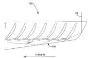
一般而言,本发明提供了一种太阳能系统,该太阳能系统用光导太阳能电池板(LGSP)来将使光陷入在介电或其它透明电池板内并且将该光传导到电池板边缘之一,用以被太阳能收集器(SEC)收获。这允许很薄的模块,这些模块的厚度相当于SEC的高度,该SEC可以是例如在该模块的边缘处的PV电池,因此消除了诸如CPV系统之类的传统太阳能系统内在的深度要求。照射该LGSP的光被改向或被向内部陷入,以便它通过该电池板的边缘之一离开该电池板,其中SEC在该边缘上接收它。 In general, the present invention provides a solar energy system that uses a light guiding solar panel (LGSP) to trap light within a dielectric or other transparent panel and conduct that light to one of the panel edges, To be harvested by Solar Energy Collectors (SEC). This allows for very thin modules, the thickness of which is equivalent to the height of the SEC which may be, for example, the PV cells at the edge of the module, thus eliminating the depth requirements inherent in traditional solar systems such as CPV systems. Light striking the LGSP is redirected or trapped inwards so that it exits the panel through one of the panel's edges where the SEC receives it. the
本发明的LGSP能够被结合成组以制造模块。该LGSP光学装置在结构上可以被设计为大部分自支撑,这意味着它们不要求任何实质性的外壳来维持它们的形状和定向。完整的外壳可以添加到该LGSP。如下面将要描述的,为了最小化材料的使用和成本,LGSP模块可以由轴加凸缘(axle-and-rib)的结构来支撑。 The LGSPs of the present invention can be combined into groups to make modules. The LGSP optics can be structurally designed to be mostly self-supporting, meaning that they do not require any substantial housing to maintain their shape and orientation. Complete shells can be added to this LGSP. As will be described below, to minimize material usage and cost, the LGSP module may be supported by an axle-and-rib structure. the
可以利用聚集的阳光作为动力以用于不同于用(PV)电池发电的目的。一个替代的用途是对元件进行加热。这些模块还可以被配置为加热水的同时进行发电。也可能的是,将聚集的光接入到光纤装置或者其它光导以将光传导到另一位置以用于某些其它用途,例如传导到照明器材以提供日光照明。 Concentrated sunlight can be harnessed as power for purposes other than electricity generation with (PV) cells. An alternative use is to heat the element. The modules can also be configured to generate electricity while heating water. It is also possible to tap the concentrated light into a fiber optic device or other light guide to conduct the light to another location for some other use, such as to a lighting fixture to provide daylighting. the
图1和图2示出本发明的LGSP 100的第一实施例的横截面视图。电池 板100具有光插入段102和光学波导段104,它们都能由任何合适的光学透射性材料制成。光插入段102在它的输入表面108接收阳光106,并且从那里开始,阳光106被导向诸如一组反射镜110之类的光学元件。这些反射镜110在光插入段102的光学透射性材料和组成区域114的材料之间的界面112来限定。选择界面112相对于入射的阳光106所位于的角度和光插入段102的光学透射性材料的折射率与区域114的材料的折射率之比,使得入射在界面112上的阳光106经历全内反射。通常,材料114是空气或任何其它合适的气体;然而,光插入段102的材料和光学波导段104的材料可以包括例如任何类型的聚合物或丙烯酸玻璃,例如,聚甲基丙烯酸甲酯(PMMA),其对于光学频谱的可见部分具有大约1.49的折射率。也可以使用任何其它合适的材料。界面112相对于入射的太阳光106所位于的角度的范围从临界角到90°,由界面112的表面法线开始测量(例如对于PMMA-空气界面,该角度基本包括在大约42.5°和90°之间)。
1 and 2 show cross-sectional views of a first embodiment of an
反射镜110被成形为抛物面反射镜;然而它们可以是任何合适的形状。如果这些反射镜之间的间隔是“A”,并且坐标系统的原点是孔径116,那么相应的抛物线的示范性公式为y=(1/2A)x2-1/4。如图1所示,每个反射镜110通过将阳光106聚焦在输出光学孔径116而将阳光106引向各自的输出光学孔径116。图2示出用相同的反射镜110对阳光106进行聚焦。如此聚焦的阳光106进入光学波导段104,光学波导段104包括壁118,阳光106被传播向壁118。壁118具有位于光学波导段104的光学透射性材料和位于壁118的另一侧面上的材料122之间的第一表面120。界面118可以位于的相对于水平方向的角度在1-5°的范围中;然而,任何其它合适的角度也将起作用。选择壁118相对于来自孔径116的阳光106的定向和光学波导段104的光学透射性材料的折射率与材料122的折射率的比率,使得入射在第一表面120上的阳光106经历全内反射。材料122可以是空气和任何其它气体;然而折射率低于光学波导段104的折射率的任何其它材料也可以组成材料122。至于光插入段102的材料和光学波导段104的材料,它们可以包括, 例如任何类型的聚合物或丙烯酸玻璃,例如,PMMA。也可以使用任何其它合适的材料。
一旦阳光106在第一表面120上被全内反射,它在光学波导段104中向一组反射元件124传播,该组反射元件124向第一表面120反射阳光106,在第一表面120上,阳光再次经历全内反射。如图3所示,每个反射元件124被在光学波导段104和组成区域128的材料之间的界面来限定,区域128的材料可以是与区域114相同的材料。选择反射元件124相对于来自第一表面120的阳光106的定向和光学波导段104的光学透射性材料的折射率与材料128的折射率的比率,使得入射到反射元件124上的阳光106经历全内反射。然而,反射元件124、第一元件120和反射镜110的功能不需要基于全内反射并且可以包括例如合适类型的反射镜。
Once the
如在图1-3中的示范性实施例所示,每个反射元件124是平面的并且与输入平面108成非平行的角度(例如1-5°)。另外,每个反射元件124位于距输入表面108基本相同的距离并且基本平行于第一表面120。同样,光学波导段104,如图3所示,一般具有楔形,其起到的作用是在楔形变宽的方向(该方向称为下行方向)上传播通过光学输出孔径116输入的阳光106。因此,光学波导段104使得在第一表面120和在反射元件124处的多个连续的全内反射之后,阳光106到达输出表面130(图1和2),输出表面130为侧壁132的一部分,其中合适类型的SEC(未示出)可以被设置以收获阳光106携带的能量。
As shown in the exemplary embodiment in FIGS. 1-3 , each
图1和2示出与输入表面108不垂直的侧壁132;然而,侧壁132可以与输入表面108成任何合适的角度。另外,如技术人员将会理解的,LGSP 100可以具有任何合适数目的反射元件124以及任何合适数目的输出光学孔径116。
1 and 2 illustrate
图3示出在该实施例中每个反射元件124与壁118平行。在该实施例中,当阳光106的射线在下游方向上传播时,入射角保持为常数。
FIG. 3 shows that each
图4示出反射元件124可以被形成为使得来自第一表面120(图1)并 且向光插入段102传播的阳光106将被反射离开反射元件124并且没有入射在输出光学孔径116上。
4 shows that
图5示出本发明的另一实施例,其中壁118和反射元件124之间的角度不平行而是在下游方向上张开。在本实施例中,可以示出的是,阳光106将保持陷入在光学波导段104中。图6示出了一实施例,其中壁118和这些反射元件之间的角度在下游方向上接近。在本实施例中,可以示出的是,阳光106最终发射出光学波导段104。
Fig. 5 shows another embodiment of the invention in which the angle between the
图7示出可以具有图1中示出的横截面图的LGSP的100透视图。图7的LGSP 100将阳光106聚集在侧壁132上。图7的LGSP 100的实施例可以被称为具有直线几何形状,因为反射镜110全部沿平行线放置。
FIG. 7 shows a 100 perspective view of an LGSP that may have the cross-sectional view shown in FIG. 1 .
对于阳光106在由X和Y轴限定的平面中的入射角的改变,图7的LGSP100的性能基本是不变的。在图8A-8C中示出了这种不变性,在图8A-8C中,分别以30°和45°入射在输入表面108上的射线134和136被光插入段102引向光学波导段104,并且在光学波导段104中朝输出表面130向下游传播。因为对X-Y平面中的入射角的这种不变性,图7的LGSP 100可以与任何合适的单轴太阳跟踪装置协同使用,以有效地将阳光106聚集在该电池板的边缘,即聚集在输出表面130。如技术人员将会理解的,单轴跟踪装置保持该电池板与太阳固定地对齐,以便使得被LGSP捕获的阳光的量最大。
The performance of the
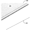
图9示出可以具有图1中示出的横截面的另一LGSP 100的透视图。图9的LGSP 100基本成形为圆板138,并且将阳光聚集在形成于圆板138的轴心区域中的内壁140上,内壁140充当输出表面142,其可以通过任何合适的路径被光耦合到任何合适的SEC。下面进一步讨论如何将阳光106耦合到SEC的实例。图9的LGSP 100的实施例被称为具有旋转几何形状态,因为反射镜110位于同心圆上。SEC包括例如光伏检测器、太阳能电池、聚集入射的阳光并且用光纤装置将入射的阳光传输到建筑物内部以用于照明材料的光纤收集器以及诸如用于对水进行加热之类的热力收集器,或者任何它们结合。
FIG. 9 shows a perspective view of another
图9的LGSP 100可以切割成如图10所示的矩形方块或者如图11所示的角形薄片,或者任何其它合适的形状,以便适于任何想要的安装架或结构(未示出)。
The
如技术人员将会理解的,图7-11的LGSP 100可以被安装到任何合适类型的太阳跟踪系统,例如,单轴跟踪系统和双轴跟踪系统。对于图7-11的LGSP 100,可以在聚集型阳光接收和有角度型阳光接收上进行设计折衷,这接下来确定所要求的对齐和跟踪精度。图7的LGSP 100可以实现例如20-50个太阳功率密度的聚集并且要求大约1°的单轴太阳能跟踪。图10的LGSP100可以实现例如大约500-1000个太阳功率密度的集中并且要求大约1°的双轴跟踪。在图10的LGSP 100的中心具有较大的轴心区域,即在LGSP 100的中心具有较大的开口将比轴心区域较小时产生更少的集中并且将要求较不精确的跟踪。
As the skilled artisan will appreciate, the
如技术人员将会理解的,光学输出孔径116的宽度与反射镜110的跨度的比率确定了该聚集。如果使该比率很小,使得光学输出孔径116非常紧,则可以使该聚集很高,然而该角型接收将很小。116的宽度和110的水平跨度的比率还影响第一表面120的角度,因为较紧的孔径允许表面118和108之间的角度更小,例如,1°。这接下来导致更小的侧墙132,因而更小的SEC。
As the skilled person will understand, the ratio of the width of the
为了制备的目的,例如图7和10的LGSP的光插入段102和光学波导段104可以形成截然不同的层,如图12所示。这在光插入段102中产生了出口面144并在光学波导段104中产生了注入面146。出口面144和注入面146不需要平行或平坦。出口面144和注入面146为光学输出孔径116的一部分。
For fabrication purposes, the
图13示出了本发明的LGSP的另一实施例的横截面图。在图13的实施例中,阳光106在光学输出孔径116处输入到光学波导段104中之前反射离开第一反射镜148、第二反射镜150以及第三反射镜152。第一、第二和第三反射镜是光学元件并且可以具有合适的形状,例如平面的、抛物线的、双 曲线的、椭圆形的和圆形的表面。
Figure 13 shows a cross-sectional view of another embodiment of an LGSP of the present invention. In the embodiment of FIG. 13 ,
此外,在光插入段102中还可以包括任何合适的光学元件,例如,透镜、菲涅耳透镜、抛物槽、卡塞格伦光学装置、温斯顿锥面以及锥形棱镜。这些光学元件需要不仅能够在该光学波导段的大体上的下游方向上传送阳光106到光学输出孔径116。光学波导段104可以与光插入段102的实施例无关,即相同的光学波导段104可以用于不同的光插入段102的实施例。
In addition, any suitable optical elements may also be included in the
图14示出了具有卡塞格伦光学装置的光插入段102的实施例。在这个实施例中,抛物面主镜154和双曲面次镜156用于将阳光106聚焦和引导在平面反射镜158处。阳光106反射离开反射镜158并且在注入面160处进入光学波导段104,该注入面160充当光插入段102的光学输出孔径。图14的实施例可以用于直线或旋转几何形状的LGSP。图14的卡塞格伦光学装置要求在主镜和次镜(分别是154和156)上以及平面反射镜158上的反射型表面。
Figure 14 shows an embodiment of an
图15示出了具有由位于光插入段102的光学透射性材料与材料166之间的界面164A和164B所限定的一组温斯顿锥面的光插入段102,材料166可以是空气或任何其它合适的气体;然而,任何其它合适的材料也可以组成材料166。选择界面164相对于入射的阳光106的几何形状和光插入段102的光学透射性材料的折射率与材料166的折射率的比率,使得入射在界面164上的阳光106经历全部内射。针对由界面164A和164B所限定的给定锥形162,入射在界面164A上的阳光106被反射向反射镜168,反射镜168接下来将阳光106引向光学输出孔径116。至于入射在界面164B上的阳光106,基于它在界面164B上反射的地方,它将被反射到光学输出孔径116,或者被反射到反射镜168,反射镜168将把它反射向光学输出孔径116。至于直接入射在反射镜168上的阳光106,它也在光学输出孔径116处被引导。在已经通过光学输出孔径116进入光学波导段104之后,阳光106可以入射在第一表面120上或者入射在反射元件124上,不管怎样,阳光106经历全内反射并且在下游方向上传播。反射镜168可以具有合适的几何形状,例如, 圆形几何形状,并且可以包括任何合适类型的反射型涂料。图15的光插入段102可以用于直线或旋转几何形状的LGSP。图15的光插入段102由于其相对宽的阳光接收角度而可以用于非跟踪太阳能电池板。
15 shows
在上述实施例中,通过减小邻近光学波导段的光学输出孔径的光学波导段104的高度来获得增加的聚集。如以上实施例所述,光学波导段104通过阳光的全内反射来传播阳光106。总的来说,如果光学波导段如图6所示向下游成锥形或会聚,则阳光将从光学波导段射出。然而,这种限制并不适用于光学波导段内的最后一次反射,因为在这一点,阳光将从光学波导段104出来。在由SEC马上收获阳光之前,阳光可以以任何合适的角度被反射,假设它仍将到达光学波导段的光学输出孔径。因为该SEC将收获阳光,所以阳光的入射角就不太重要,而且同样阳光在被收获之前马上被收缩或者进一步聚集。以这种方式可实现的另外的聚集依赖于阳光106在光学波导段104内的角展度,可实现的聚集越大,光导层内的阳光就越平行。在通常的实施例中,例如,额外聚集的范围可以在1.5倍到2倍之间。
In the embodiments described above, increased concentration is obtained by reducing the height of the
增加这种额外聚集的最简单的方式是使靠近SEC的光导层成锥形。用于聚集的好的锥形是温斯顿锥面,其为离轴抛物面,它的一个实例在图16中以附图标记170来表示。然而,包含这种温斯顿锥面170在LGSP 100中引入了死区(被定义为暴露给阳光的、不捕获光和向SEC发射光的LGSP表面),因为入射在温斯顿锥面上的光基本没有被捕获。这种死区导致,在使用用于将太阳能转换成有用能的空间的利用上,总的系统效率降低。
The simplest way to add this extra concentration is to taper the lightguide layer close to the SEC. A good cone shape for concentrating is the Winston cone, an off-axis paraboloid, an example of which is indicated at 170 in FIG. 16 . However, inclusion of this Winston cone 170 introduces a dead zone (defined as the LGSP surface exposed to sunlight that does not capture light and emit light to the SEC) in the
额外聚集和死区之间的折衷可以利用图17示出的半温斯顿锥面来实现。作为另一替代,如图18所示,平坦的有小平面的锥形174可以用于估计温斯顿锥面的效果。然而,该平坦的有小平面的锥形并不提供可以与温斯顿锥面提供的相同的额外聚集。尽管存在这样的事实,但因为平面元件比弯曲元件更容易制备,所以图18示出的方法可能是令人感兴趣的。
The trade-off between extra aggregation and dead space can be achieved with half Winston cones as shown in FIG. 17 . As another alternative, as shown in FIG. 18, a flat
利用分离的光学元件,即由光学透射性材料制成并且可以被固定在光学波导段和SEC(未示出)之间的收缩,来实现增加的聚集。这种收缩在图 18中以附图标记176来表示。如果收缩176的折射率大于光学波导段的折射率,则可以获得进一步的额外聚集。因为在光学波导段和收缩176之间的界面180处出现了阳光偏转并且因为高折射率材料(收缩176)的临界角更小,所以出现了额外聚集。
The increased concentration is achieved using a separate optical element, ie a constriction made of optically transmissive material and which can be fixed between the optical waveguide section and the SEC (not shown). This shrinkage is indicated with
在光学波导段和SEC之间放置例如收缩176的优点在于它可以将光学波导段与SEC处的热积聚绝缘。在条件很差的操作期间,如果SEC变得比制成光学波导段的材料所能承受的更热,则这变得很重要。
An advantage of placing eg a
图19中示出了本发明的LGSP 100的另一实施例。该实施例允许光学波导段104提供阳光给固定到由光学波导段104限定的一组壁182的一组SEC。如技术人员将会理解的,使用多个壁182导致更薄的光学波导段104。
Another embodiment of the
为了保护光插入段102的输入表面108和光学波导段104的第一表面120,图20中示出的覆层184可以涂抹到该输入表面和/或涂抹到该第一表面。该覆层可以具有比该光插入段的折射率更低并且比该光学波导段的折射率更低的折射率。此外,覆层184还可以被涂抹在LGSP 100内通常被空气或气体所占据的空间内。
To protect the
具有这种覆层184的优点在于,它可以保护该LGSP的完整性。有了这种覆层184存在,该覆层的外表面可以变脏或被刮擦而不会危及该LGSP的功能。覆层184可以由诸如氟化乙烯丙烯之类的任何合适的材料制成。如技术人员将会理解的,该覆层的厚度可以相对变薄而且仍然是有效的。
An advantage of having this
以上给出的这些LGSP实施例是可伸缩的。也就是说,它们的尺寸可以乘以一公共因子完全改变而不会影响这些光学装置的功能,假设这些光学装置没有变得小到使得干扰效应占优势。当交错的光学装置之间的空间处于与光波长相当的数量级时,这些干扰效应可能变得很重要。太阳频谱的最高能量波长部分在0.2微米到3微米之间。相应地,可以将这些光学元件和这些孔径的交错周期以及这些孔径的尺寸保持在大于3微米以消除这些干扰效应。 The LGSP embodiments given above are scalable. That is, their dimensions can be varied entirely by a common factor without affecting the functionality of the optics, provided that the optics do not become so small that interference effects predominate. These interference effects can become significant when the space between interleaved optics is on the order of the wavelength of light. The highest energy wavelength portion of the solar spectrum is between 0.2 microns and 3 microns. Accordingly, the interleaved period of the optical elements and the apertures and the size of the apertures can be kept greater than 3 microns to eliminate these interfering effects. the
为了使用最少的材料并保持低的成本,想要的是,使这些光学元件体积 变小以最小化LGSP的厚度并且使得能够以最少的材料覆盖最多的面积。光学波导段(光导层)的厚度将大大受限于这些被布置成收获阳光的SEC的尺寸(例如PV电池条)。在PV电池条的情况下,它们的尺寸可以变化,例如,从1毫米到1分米,虽然更大或更小的PV电池会工作的同样好。另一方面,光插入段(插入层)可以被制成薄到干扰效应和制备方法所能允许的程度。 In order to use the least amount of material and keep the cost low, it is desirable to make these optics compact to minimize the thickness of the LGSP and enable the most area to be covered with the least amount of material. The thickness of the optical waveguide section (lightguide layer) will be largely limited by the size of those SECs (eg PV cell strips) that are arranged to harvest sunlight. In the case of PV cell strips, their size can vary, for example, from 1 millimeter to 1 decimeter, although larger or smaller PV cells will work equally well. On the other hand, the optical insertion section (intercalation layer) can be made as thin as interference effects and fabrication methods allow. the
本发明的这些LGSP可以由诸如喷射模塑、压缩模塑、喷射-压缩模塑之类的模塑技术或者通过任何其它合适的方法来制备。一般而言,通过模塑方法制成的部分不可以有底切,并且同样利用常规模塑一次模塑整个上述光导电池板是不可能。然而,该LGSP可以通过将它们分成可以被单独地模塑的段来制造。下面描述两个用于为了制造的目的分割LGSP的示范性方法。 The LGSPs of the present invention may be prepared by molding techniques such as injection molding, compression molding, injection-compression molding, or by any other suitable method. In general, the parts made by the molding method must not have undercuts, and it is also impossible to mold the entire above-mentioned photoconductive cell plate at one time by conventional molding as well. However, the LGSPs can be fabricated by dividing them into segments that can be molded individually. Two exemplary methods for segmenting LGSPs for manufacturing purposes are described below. the
第一种方法是制造薄的LGSP的垂直部分或薄片,并且如图21所示对它们进行并排装配。该电池板的分离的薄片190可以通过外拉(未示出)固定在一起,或者它们可以被粘合在一起或者相反被绑定在一起。第一种方法(薄片方法)适于直线几何形状LGSP。 The first method is to fabricate thin vertical sections or slices of LGSP and assemble them side-by-side as shown in FIG. 21 . The separate sheets 190 of the panel can be held together by pulling them out (not shown), or they can be glued together or otherwise bound together. The first method (thin slice method) is suitable for straight line geometry LGSP. the
第二种方法是制备水平板材以制作LGSP,这些板材可以是一个在另一个顶上堆叠的板材。这样的电池板可以是自支撑的,对在框架和外壳上要求很少并且可以使得不需要粘合和绑定。这些板材组成先前描述的功能层(光插入段和光学波导段);然而,给定的功能层可以由任何数目的板材组成。 The second method is to prepare horizontal sheets to make LGSP, these sheets can be sheets stacked one on top of the other. Such panels may be self-supporting, requiring little on the frame and housing and may render gluing and binding unnecessary. These sheets make up the previously described functional layers (optical insertion section and optical waveguide section); however, a given functional layer may consist of any number of sheets. the
图22A-22D是一种将LGSP 100分成三个薄板而没有底切的方式。顶部的两个薄板192和194共同起作用形成插入层(光插入段102),底部的薄板196形成光导层(光学波导段104)。图22A-22D示出的实施例类似于图13示出的实施例。在顶部板材192中,阳光106通过全内反射(TIR)的方式反射离开抛物面反射镜,它然后从顶部板材192出来,并进入中间板材194,然后在从中间板材194出来并进入底部板材196之前通过TIR方式反射离开两个平坦的小平面,该底部板材196充当光导层(光学波导段104)。
Figures 22A-22D are one way of dividing
图23A-23C示出另一种可能的将LGSP 100分成两个板材198和200。 该插入层和光导层各用一个板材来制作,分别是板材198和200。如图24A所示,阳光106全内反射离开抛物表面202而后在遇到光导层(光学波导段)的注入面206之前通过平坦的小平面(出口表面)204出来进入到空气中。在插入层板材的出口表面204处的偏转改变了该抛物面反射镜的焦点;它使得该焦点稍微向上,这接下来要求向上移动光导层的孔径。稍微移动焦点有一个优点:它允许捆紧抛物面反射镜面而它们之间死区很小。然而,使用偏转而非仅仅反射来聚集阳光的缺点在于得到的实施例在单轴阳光跟踪的情况下不会发挥最佳的作用。同样,图24A的两板材式方法非常适合于旋转几何形状的LGSP。这是因为无论如何,为了最优性能,该实施例要求两个轴跟踪。通过平坦的小平面改变焦点将一些小的散光引入到聚焦抛物面光学装置。这将阳光106略微散布在焦点,并且将可实现的聚集限至到一定程度。通过略微倾斜该抛物面来稍微补偿该散光是可能的。如果该平坦小平面204从垂直线沿逆时针方向倾斜2°,则从垂直线沿顺时针方向将抛物面反射镜倾斜5°可以稍微补偿该散光。图24B示出类似于图24A的光导太阳能电池板的光导太阳能电池板的另一实施例,但是改为具有与由注入面206形成的突起207相邻的三次曲面203。
23A-23C illustrate another possible division of
图24C示出图24B的光插入段的周期性单元的示范性尺寸,正在讨论的该单元包括三次曲面203、平坦的小平面204、注入面206和突起207。这些长度以微米为单位,并且三次曲面203的方程为y=-1.049388x+9.1781775×10-4x2+1.19193×10-7x3。
FIG. 24C shows exemplary dimensions of the periodic unit of the optical insertion segment of FIG. 24B , the unit in question comprising
图25A-25C示出了又一将LGSP 100分成两个板材208和210,其改进了图24A的实施例的关于非最优单轴跟踪的限制,并且允许制备一种不使用偏转来聚集阳光的直线几何形状LGSP。如图26所示,阳光106全内反射离开抛物面反射镜212,但是在该实施例中,它在出口面214处从插入层板材出来,该出口面214是以抛物面反射镜212的焦点为中心的圆的圆弧。会聚在抛物面反射镜的焦点的阳光线各以基本上直角碰到该弧形出口面,并且因此没有发生偏转。
Figures 25A-25C show yet another division of the
所有以上提及的板材,在它们被装配成LGSP时,可以用使它们之间的对齐变得容易的装配特征来模塑。这些装配特征对光学性能可以具有最小的或没有干扰。特别地,本发明的LGSP的实施例可被设计为使得上游孔径的背部依靠在抛物面反射镜的底部;这是具有图25C的实施例的实施例。其它装配特征可以包括散布在光导层的表面上的小结块,这些小结块将这些抛物面反射镜相对于光学波导段104固定就位。这些板材之间的空间将基本清除灰尘和潮气。这些板材可以用硅树脂或任何其它合适的材料或者利用密封垫或任何其它合适的封条彼此密封。小量的干燥剂可以添加在这些板材之间来吸收潮气。防尘套或全防护壳可以被添加到该LGSP来保持它清洁并且允许与结构相匹配的颜色。
All of the above mentioned panels, when they are assembled into LGSP, can be molded with assembly features that facilitate alignment between them. These assembly features may have minimal or no interference with optical performance. In particular, an embodiment of the LGSP of the present invention can be designed such that the back of the upstream aperture rests on the bottom of the parabolic mirror; this is an embodiment with the embodiment of Figure 25C. Other mounting features may include small nodules scattered on the surface of the lightguide layer that hold the parabolic mirrors in place relative to the
图27示出了单轴跟踪太阳能系统216。单轴跟踪太阳能系统216可以使用利用两板材式方法来制造LGSP 100,并且可以被装配成围绕轴218倾斜。这些LGSP可以被制成正方形,每个边长125毫米。光导层(光插入段)可以使用半温斯顿锥面来将阳光聚集到3米高的PV电池上。这种系统的光学聚集大约是30个太阳功率密度。
FIG. 27 shows a single axis tracking solar system 216 . A single axis tracking solar system 216 can be fabricated using a two-sheet approach to
系统216用在吸热器220的任一侧排列成两个平行排的若干(例如,10个)太阳能电池板100来形成,吸热器220可以由铝或任何合适的材料制成,并且采用这样一种方式,即将光聚集向这些电池板的连接到吸热器220的内部边缘。PV电池被放置在光学电池板100和吸热器220之间。
The system 216 is formed with a number (e.g., 10) of
太阳能电池板100可以通过图28示出的凸缘222保持对齐。这些凸缘可以由喷射模塑聚合物制成,虽然可以使用机器加工铝或任何其它材料。凸缘222靠着吸热器220将电池板100机械地固定就位,并且可以在凸缘222和吸热器220上包含一些特征件以方便装配。这样的特征件(例如凹槽224)和凸缘222和吸热器220的细节分别在图28和29中示出。可以使用机械紧固件、粘胶或任何其它手段将凸缘222靠着该吸热器固定就位。
The
该吸热器220可以起两个作用:(1)它辅助从PV电池散热,并且(2)它为LGSP 100生成刚性支撑轴。在吸热器220的任一侧上对这些电池板的 重量进行平衡,并且吸热器220在这些电池板连接到外部支撑架的地方。为了辅助散热,并且如图29所示,吸热器220可以具有散热片226,散热片226由粘结在两个挤压铝轨道228之间的折叠铝片制成。这些散热片被连接到这两个轨道并在吸热器220中生成垂直空气通道230。可以通过铜焊、环氧树脂、型锻或通过其它手段来进行这些散热片与这两个轨道之间的粘结。这种开口吸热器实施例允许通过自然对流来散热,因为热空气可以从吸热器220上升出来并且较冷的空气可以从下面进入到吸热器220。
This
在系统216中使用的PV电池可以是任何尺寸,例如125毫米乘125毫米,并且可以切割成任何高度的条,例如本实施例所用的3mm高。PV电池可以以任何常规方式进行封装。例如,它们可以成串焊接在一起,并且用乙烯一醋酸乙烯(EVA)或任何其它合适的材料进行封装。可替代地,可以通过将PV电池焊接、粘附或粘结到导热介电基板上的图案式电路来进行电气连接。诸如那些明尼苏达州臣哈森市的贝格斯公司销售的绝缘金属基板(IMS)将是适合的。图30示出焊接到PV电池234的IMS基板232;以235示出该焊接层。IMS 232可以通过环氧树脂或粘胶或通过任何其它适合的手段连接到铝吸热器220。
The PV cells used in the system 216 can be any size, eg 125mm by 125mm, and can be cut into strips of any height, eg 3mm high as used in this example. PV cells can be encapsulated in any conventional manner. For example, they may be welded together in strings and encapsulated with ethylene vinyl acetate (EVA) or any other suitable material. Alternatively, electrical connections may be made by soldering, adhering or bonding the PV cells to patterned circuits on the thermally conductive dielectric substrate. Insulated Metal Substrates (IMS) such as those sold by Bergs Corporation of Chanhassen, Minnesota would be suitable. FIG. 30 shows an
通常的IMS 232具有位于被粘结到铝或铜基底的聚合物绝缘层的顶部上的铜电气图案。放弃该基底而将电气图案聚合物绝缘层直接固定到吸热器220也是可能的。可以在烘箱中通过热养护进行该过程。这个方法的优点在于它消除了基底元件并且可以降低成本。PV电池234可以通过连接到PV电池232的顶部连接器(未示出)的整个长度上的导电带或网粘结至IMS232。PV电池232的背部连接器也可以粘结到它的整个长度和/或表面上。对于长而窄且脆的PV电池232,使用上述连接方法允许这些PC电池断成段而不丧失其功能性或基本影响电力生产。
A
PV电池可以被封装来防止受潮以避免腐蚀。这可以通过诸如乙烯一醋酸乙烯(EVA)之类的任何合适的封装来实现。然而,EVA要求热固化,因而要求密封的部件需要放置在烘箱中。另一种方法是使用密封剂,其在室 温下固化在适当的位置。某些在光学上透明的粘胶,例如,道康宁生产的硅酮Sylgard184,可以起到这个目的的作用,并且可以在焊接之后在PV电池的顶部浇注成薄层。作为添加的好处,在硅酮已经开始固化之前,这些电池板可以被固定在适当位置。这密封了这些电池板和这些PV电池之间的空间,并且生成它们之间的光学粘结。这些光学电池板与这些PV电池之间的光学粘结减少了该光学电池板的出口边缘的菲涅尔损耗。
PV cells can be encapsulated to protect from moisture to avoid corrosion. This can be achieved by any suitable encapsulation such as ethylene vinyl acetate (EVA). However, EVA requires heat curing, so parts requiring sealing need to be placed in an oven. Another method is to use a sealant, which cures in place at room temperature. Certain optically clear adhesives, such as the
这些LGSP可以被排布在安装框架上以形成太阳能系统。这些吸热器可以与该安装框架上的轴承连接,该安装框架允许该电池板围绕由吸热器220制成的轴自由转动(参见图27中的轴218)。吸热器220可通过喷射模塑端帽(图27的236)的方式与这些轴承连接,该喷射模塑端帽接合到吸热器220的端部。这些端帽可以具有允许连接到该框架上的这些轴承上的任何合适的特征件。端帽236可以机械地、使用环氧树脂、粘胶、使用胶带或通过任何其它合适的手段接合到该吸热器。吸热器220的端帽236还可以耦合到允许执行器控制LGSP 100的转动的机构。例如,如图31所示,三个连杆机构可以将所有模块连接到由线性执行器240驱动的单轨238。可替代地,每个LGSP可以具有附接到支架上的小齿轮,该支架又由线性执行器驱动。用任一系统,移动该单轨的单个线性执行器可以驱动所有这些电池板的运动,使得它们一致地倾斜并且保持对齐。
These LGSPs can be arranged on a mounting frame to form a solar system. These heat sinks can be connected with bearings on the mounting frame which allows the panel to rotate freely about an axis made of heat sinks 220 (see axis 218 in Figure 27). The
可以使用具有旋转几何形状的LGSP制作并使用在图23A-23C中举例如说明的两层式方法制造全阳光跟踪太阳能电池板系统。这些全阳光跟踪系统的外观可以类似于以上针对单轴跟踪系统描述的全阳光跟踪太阳能电池板系统的外观,在该单轴跟踪系统中,LGSP可以沿中心吸热器的任一侧排列并被凸缘支撑。 A full sun-tracking solar panel system can be fabricated using LGSP with rotated geometry and using the two-layer approach illustrated for example in Figures 23A-23C. The appearance of these full sun-tracking systems can be similar to that of the full sun-tracking solar panel systems described above for single-axis tracking systems where LGSPs can be arrayed along either side of a central heat sink and Flange support. the
这些电池板的外部尺寸可以是125毫米乘250毫米。阳光被集中到位于如图32A和32B所示的LGSP的内缘的中心的线242上。阳光在半圆柱面244处从太阳能电池板100出来并进入到空气间隙中。尽管原则上薄PV电池可以沿线242放置,但这种装置会有有限的有角度的接收。
The external dimensions of these panels can be 125 mm by 250 mm. Sunlight is concentrated onto a
在实践中,较宽的有角度接收通过将屋脊棱镜246放置到半圆柱小平面来实现,如图33A-33C所示。该屋脊棱镜246可以由玻璃或任何其它合适的材料制成,并且具有大于1.4的折射率。诸如三向连接构造电池之类的高效率PV电池可以使用硅树脂密封剂或其它光学环氧树脂在光学上粘结到屋脊棱镜的基底248。图33D-33G示出矩形光导太阳能电池板800如何可以用两个光插入段部分802和804来制作。光插入段部分802和804各具有旋转的几何形状和相应的光学波导段部分806和808。入射到光插入段802的阳光被耦合到光学波导段部分806,光学波导段部分806将该阳光传播至表面810。至于入射到光插入段804的阳光,它被耦合到光学波导段808,光学波导段808将该阳光传播至表面812。表面810和812可以是平坦的表面并且任何适合的SEC可以被固定于此。由于不必使用棱镜来耦合从光学波导段部分806和808出来的光,所以可以避免菲涅尔折射损耗。如图33E所示,光学波导806和808可以具有半温斯顿锥面剖面816和818。图33F示出了光导太阳能电池板800可以采用两层式工艺通过将光插入段802和804放置在光学波导段806和808上来制作。图33G示出图33E的装置的分解视图。假定阳光从该光学装置的两侧射出,吸热器可以被放置在该电池板的各个对立的侧面。因为图33D的这个电池板并不具有耦合棱镜,所以与表面810和812相邻的光学波导段806和808的部分可以由绝缘材料制成,这种绝缘材料可以耐受更多的热量,例如,熔融石英,而其它部分由PMMA制造。
In practice, wider angled reception is achieved by placing
尽管与图33A-33C相关的上述排布(关于阳光从半圆柱面224出来而后被棱镜246直接引导至PV电池)确实是将菲涅尔损耗引入到该系统中,但是它也将一层气体,即空气或诸如氩之类的任何其它合适的气体,放置在直接接触该PV电池的棱镜246和该LGSP之间。这种排布的优点在于它防止该光学装置(该LGSP)受到可以积聚在该PV电池上的热。该PV电池在热集中的情况下可以变得很热,或许达到120℃或者更高,并且如果该光学电池板由PMMA制造,这将不利地影响该光学电池板。该气体层可以使该光学电池板绝缘并且不受到积聚在该PV电池上的热。
While the above arrangement in relation to Figures 33A-33C (regarding sunlight exiting the semi-cylindrical surface 224 and being directed by the
如之前提及的,当用于与太阳的全跟踪一起工作时,使用旋转几何学形状并为高太阳能集中而设计的LGSP提供了更好的性能,维持太阳射线在+/-1°的范围内平行于该太阳能电池板的输入表面的法向量。该全跟踪可以由若干种方式来实现,但是两种方法特别适合于该系统。 As mentioned before, when used to work with full tracking of the sun, LGSP using rotational geometry and designed for high solar concentration provides better performance, maintaining the sun's rays within +/- 1° Inner normal vector parallel to the input surface of the solar panel. This full tracking can be achieved in several ways, but two methods are particularly suitable for this system. the
图34示出了第一种全跟踪方法,其中LGSP 100安装在框架249中以围绕第一组轴250倾斜,并且框架249可以围绕轴252倾斜,轴252基本垂直于轴250。同样,该LGSP可以从东到西摆动以在全天当中跟踪太阳的移动,而且该框可以从北到南倾斜以适于太阳的季节性变化。
Figure 34 shows a first full tracking approach, where the
图35和36示出了允许维持较低的剖面的第二种全跟踪方法。LGSP 100可以设置在框架254或256中,并且可以分别绕轴258和260倾斜。此外,框架254和256可以被制成分别绕轴262和264旋转。
Figures 35 and 36 show a second full tracking method that allows a lower profile to be maintained.
图37示出了如图15所示的在插入层(光插入段102)中使用温斯顿锥面的LGSP的变体。图37的实施例是直线几何形状的实施例,其充分适合于非跟踪应用,因为它由于温斯顿锥面而具有宽的有角度的接收。为了提高可实现的聚集,使用位于两个光学电池板之间双面PV电池266是可能的;该实施例使该聚集加倍。
FIG. 37 shows a variant of LGSP as shown in FIG. 15 using Winston tapers in the insertion layer (optical insertion section 102). The embodiment of Fig. 37 is a linear geometry embodiment which is well suited for non-tracking applications as it has a wide angular acceptance due to the Winston cone. To increase the concentration achievable, it is possible to use a
图37的LGSP 100可以用两部分堆叠来制作,但是不是对每个PV电池带的太阳能电池板进行模塑,而是可以对一组电池板进行模塑,一组光学电池板由许多聚光器光学装置集合成较少的片。图38示出如何可以将一组LGSP 268制成容纳四个PV电池266。
The
形成光导层(光学波导段104)的板材270可以具有模塑在其中的凹槽,以容纳双面PV电池266。PV电池266可以被焊接而后在放置到该凹槽中之前被封装,或者它们可以仅仅被焊接在一起以形成电路而后放置在该凹槽中并且使用现场浇注的诸如透明硅或任何其它光学环氧树脂之类的密封剂封装就位。
The sheet 270 forming the light guiding layer (optical waveguide segment 104 ) may have grooves molded into it to accommodate the double-
将许多组电池板附接在一起组成全太阳能电池板模块。存在许多将这些LGSP结合在一起的方法。一种方法是使用框架格栅将所有这些电池板绑在 一起。另一方法是将这些光学电池板排列并通过任何合适的手段粘结在玻璃或任何其它材料的坚硬上层上。 Many sets of panels are attached together to form a full solar panel module. There are many ways to bring these LGSPs together. One way is to use a frame grid to tie all these panels together. Another approach is to align and bond these optical cell panels to a rigid upper layer of glass or any other material by any suitable means. the
如在图37中看到的,在该光学装置的横截面中,非跟踪LGSP 268一般不会具有180°的有角度的接收。LGSP 268的接收锥面可以是从该电池板的法线起+/-30°,这足以适应天空中的太阳位置的季节性变化。同样,非跟踪LGSP 168应该安装在与安装位置的纬度相匹配的斜面上;这将保证该电池板的输入表面的法线在昼夜平分点平行于太阳的射线。然而,这确实限制了非LGSP 268的安装结构。实际上,如针对北半球位置的图39所示,LGSP 268可以被设计为使它们的接收锥面倾斜离开该法线。在实践中,有限数目的非跟踪LGSP 268组可以被设计为适应于任何安装结构。
As seen in Figure 37, in the cross-section of this optic, the non-tracking LGSP 268 generally does not have 180° angled acceptance. The receiving cone of the LGSP 268 can be +/-30° from the normal to the panel, which is sufficient to accommodate seasonal variations in the sun's position in the sky. Likewise, the
为了尽可能成本经济地制作本发明的LGSP,卷对卷连续铸造或压花可以用于将光插入段光学装置制备成膜。用卷对卷制造方法是可能的,因为所有以上太阳能电池板由不具有底切的板材的堆叠组成。成楔形的光导层(光学波导段)可以分开制作,并且光插入段可以利用层压工艺或任何其它合适的工艺敷设到光学波导段上。 In order to make the LGSP of the present invention as cost-effective as possible, roll-to-roll continuous casting or embossing can be used to make light insertion segment optics into films. It is possible with a roll-to-roll manufacturing method, since all the above solar panels consist of a stack of sheets without undercuts. The tapered optical waveguide layer (optical waveguide section) can be fabricated separately and the optical insertion section can be applied to the optical waveguide section using a lamination process or any other suitable process. the
如技术人员会理解的,本发明的LGSP的光插入层102还可以使用任何类型的透镜作为光学元件而非仅仅对上述TIR界面进行聚焦。图40示出具有一组透镜274的LGSP 100,该组透镜274聚焦并光耦合阳光106到光学波导段104。
As the skilled person will understand, the
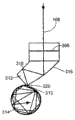
本发明的LGSP的另一实施例如图41A、41B和42A-42D所示。LGSP 300具有插入层(光插入段302)和光导层(光学波导段304)。光插入段302具有采用偏转器部分306和反射镜部分312形式的光学元件。反射镜部分306使入射的阳光106在由双箭头308指示的一个或两个方向上偏转。偏转的阳光被引导向光学元件。这些光学元件是反射镜部分312,其被成形为一组聚焦锥形光通道。这些锥形光通道通过一组光学输出孔径313被光耦合到一组波导314,该组波导314形成光学波导段304。
Another embodiment of the LGSP of the present invention is shown in Figures 41A, 41B and 42A-42D. LGSP 300 has an insertion layer (optical insertion section 302) and an optical guiding layer (optical waveguide section 304).
偏转器部分306可以包括采用体相位全息图(VPH)的形式的光学引导 层。利用两个相干UV光源之间的干涉,以任何合适的形式形成VPH全息图中的条纹。条纹间距和角度可以被设计成使得一个或者更多衍射模式可以在太阳能电池板的平面的45度的范围内。图42A示出这种VPH 309如何进行操作的实例。在图42B至42D中举例说明了得到的偏转。
The
偏转器部分306还可以利用诸如象棱镜一样的平坦的小平面光学装置之类的非干涉光学装置来制作。例如,以互锁方式设置的之间具有小的空气间隙的60°棱镜阵列将入射光在两个方向上分割到该电池板的平面上。该双向偏转将导致光积聚在太阳能电池板300的两个对立的边缘上。在图43中示出了这样的引光导学装置。
The
光学波导段304具有直线几何形状并且可以具有多个波导314,波导314从它们各自的锥形光通道(反射镜部分312)接收光并且通过全内反射来使光陷入。波导314充当延迟线,由此光在光学输出孔径313处从高处进来,传播一段距离而后可以通过光学输出孔径313从顶部出来。在图42A-42C示出了可能的通道实施例。进入锥形光通道(反射镜部分312)的光被反射离开第一抛物线部分316,而后离开平面318并且在进入限定波导314的圆柱部分之前离开第二抛物线部分320。该光在射出之前可以以螺旋方式在波导314内传播一些距离。假设波导314的长度小于锥形光线的平均传播距离,耦合到波导314的光将从该通道的端部集中地射出,由任何合适的SEC在该通道收获光。作为实例,如果光学波导段104高1cm,并且波导314长150cm,则入射到LGSP 300上的光的75%将到达用于由SEC进行收获的该波导的两端。如果光被均匀地入射到LGSP 300上,则光将均匀地分布在该波导通道的两端之间。
The
LGSP 30可以包括任何数目的波导314以及锥形光通道312,并且每个波导314可以形成一个具有各自的锥形光通312的单元。由该锥形光通道312形成的这些单元和它们各自的波导314可以通过模塑来制作。
LGSP 30 may include any number of
在LGSP 300中,每个波导314具有输出表面315,并且输出表面315的总和形成光学波导段304的全部输出表面。任何合适的SEC可以被放置 在多个光学输出孔径315的输出端以收获阳光106。
In LGSP 300, each
可以使用锥形光通道/波导的其它几何形状。例如,图44A-44C示出了具有多个形成在其上的波导的锥形光通道232,该波导的直径随着锥形光通道的宽度的减小而减小。这些波导的交错在垂直方向上允许两个或更多通道并排靠近放置,它们之间具有很小的死区。
Other geometries of tapered light channels/waveguides can be used. For example, FIGS. 44A-44C illustrate a tapered
先前描述的吸热器220可以与单轴跟踪系统和全跟踪高聚光型系统协同工作,以从SEC(例如PV电池)将过剩的热量散发到周围的空气中。然而,该过剩的热量可以改为用于加热水。该功能性可以用图45A和45B示出的吸热器400来完成。吸热器400可以由铝或其它适合的材料制成。与以散热片为特征以将过剩的热量散发到空气中的吸热器220相反的是,吸热器400具有一个或更多通道402,用于流过吸收这些SEC中产生的热量的水。
The previously described
如在图46见的,端帽403可以固定到吸热器400并且起到将LGSP通过轴承固定到安装框架的双重目的的作用,并且它们用作到热交换器(未示出)的入口和出口。水可以直接流过的吸热器400,吸热器400的一端有端帽另一端有出口;或者它能够通过相同的端帽流入或流出该吸热器400,吸热器400具有用作u型管的对立的端帽。在扩展的系统中,这个实施例可以简化在许多模块之间的软管路线。挤压的通道的数目可以增加以便在水和吸热器400的铝之间具有较大的接触表面区域。水流过吸热器400的速率可以用于控制这些SEC的温度并且用于将LGSP保持在它们的工作温度范围内。在图46示出了使用通过软管406互联的吸热器400的系统。如技术人员将会理解的,除水之外的热交换器流体可以用于图46的系统。
As seen in Figure 46, the end caps 403 can be secured to the
由本发明的LGSP捕获的阳光可以用于不使用PV电池的太阳能系统。在图47中示出了这种太阳能热力系统500的实例。系统500可以使用双壁管502,它的最外面管是透明的。诸如氩之类的绝缘气体将内管与外管分离。内管可以是黑色的以便吸收入射的阳光。通过中心管,流过诸如水、油之类的吸热液体或任何其它合适的液体。 Sunlight captured by the LGSPs of the present invention can be used in solar systems that do not use PV cells. An example of such a solar thermal system 500 is shown in FIG. 47 . The system 500 may use a double walled tube 502 whose outermost tube is transparent. An insulating gas such as argon separates the inner tube from the outer tube. The inner tube may be black to absorb incident sunlight. Through the central pipe, a heat absorbing liquid such as water, oil or any other suitable liquid flows. the
管502被放置在先前被上述实施例中的吸热器占据的位置。聚集的阳 光,穿过透明的外管以及绝缘气体层,并且被内管吸收。这使得内管中的液体被加热。这些流体传送管可以保持固定在合适的位置,同时光学装置绕它们旋转。 Tube 502 is placed in the position previously occupied by the heat sink in the above embodiments. The concentrated sunlight passes through the transparent outer tube and insulating gas layer and is absorbed by the inner tube. This causes the liquid in the inner tube to be heated. These fluid transfer tubes can remain fixed in place while the optical device rotates about them. the
用一种被称为在玻璃上的硅树脂的技术制备本发明的LGSP的一些小光学结构。类似于道康宁(Dow)生产的SylgardTM84的薄的透明硅橡胶,在玻璃基板上形成为需要的形状。对硅树脂进行独立的模塑而不用玻璃基板也是可能的。 Some small optical structures of the LGSP of the present invention were prepared using a technique known as silicone-on-glass. A thin transparent silicone rubber similar to Sylgard ™ 84 from Dow was formed into the desired shape on a glass substrate. It is also possible to independently mold silicone without using a glass substrate.
有利的是,本发明的LGSP对热膨胀或收缩相对不敏感。这是可能的,因为这些太阳能电池板的所有光学组件是由相似的(如果不相同的话)材料制成。因为这一点,它们将膨胀相同的程度并且光学元件的功能将不会显著改变。具体来讲,随着反射镜110膨胀,波导部分104也将膨胀。随着该单元根据温度的变化而膨胀或收缩,这维持相同的焦点,使得光从图1的106反射离开110并在116聚焦。
Advantageously, the LGSPs of the present invention are relatively insensitive to thermal expansion or contraction. This is possible because all the optical components of these solar panels are made of similar, if not identical, materials. Because of this, they will expand to the same extent and the functionality of the optics will not change significantly. Specifically, as
对于单轴跟踪,该电池板被倾斜以维持与入射的阳光在一个平面上对齐。在该光学装置的顶上添加光学设备也是可能的,其对光进行预处理,改变入射光的角度以将入射光对准该光学装置。这种预处理光学装置可以使用移动式反射镜、棱镜或电光装置。 For single-axis tracking, the panel is tilted to maintain alignment in a plane with the incoming sunlight. It is also possible to add optics on top of the optics that pre-process the light, changing the angle of the incident light to direct it towards the optics. Such preconditioning optics can use moving mirrors, prisms, or electro-optic devices. the
通过必要时使单轴跟踪电池板或非跟踪电池板倾斜来手动实现跟踪。手动跟踪电池板将是一个在横截面中具有足够宽的有角度的接收的跟踪电池板,比方说,例如,正或负5度,以便它将仅仅需要每隔几周稍微手动重新对齐。电子对齐传感器可以帮助对齐,而不会需要执行器。 Tracking is accomplished manually by tilting single-axis tracking panels or non-tracking panels as necessary. A manual tracking panel would be one that has an angled reception wide enough in cross-section, say, for example, plus or minus 5 degrees, that it would only require slight manual realignment every few weeks. Electronic alignment sensors can aid in alignment without the need for actuators. the
使用不同机构的LGSP可以利用一个具有梯度折射率的电池板来制成。在该LGSP的下游方向折射率梯度增加,以便在该电池板上的入射光将偏转向下游方向。如果该梯度造成在该电池板的底面发生针对TIR的足够偏转,则该光将成锥形并且将变为向下传导向该电池板的边缘,如图48所示。由于梯度较小,如果光从该电池板的底面出来,可以要求反射镜进行第一次反射,并且在向回传播通过该电池板到顶表面的同时,进一步的偏转将增加在 顶面上的入射角,足够使TIR发生。这在图49中示出。 LGSP using a different mechanism can be fabricated using a gradient-index panel. The refractive index gradient increases in the downstream direction of the LGSP so that incident light on the panel will be deflected in the downstream direction. If the gradient causes sufficient deflection for TIR to occur at the bottom surface of the panel, the light will be tapered and will become directed down towards the edge of the panel, as shown in FIG. 48 . Due to the small gradient, if light comes out of the bottom surface of the panel, the mirror can be required to make a first reflection, and further deflection will increase the incidence on the top surface while propagating back through the panel to the top surface angle, enough for TIR to occur. This is shown in Figure 49. the
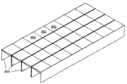
图50A和50B示出图33D的诸如光导太阳能电池板800之类的光导太阳能电池板如何可以被组在一起。光导太阳能电池板800可以被放置在两个垂直方向的铝吸热器900之间以形成光导太阳能电池板800的直线装置902。较大组的光导太阳能电池板800可以通过将直线装置902接合在一起来装配。
50A and 50B illustrate how lightguide solar panels such as lightguide
本发明是一种使用LGSP来将光陷入在介电或其它透明电池板内并将该光传播到电池板边缘之一用于由SEC进行捕获的太阳能系统。这允许很薄的模块,这些模块的厚度相当于在该模块的边缘的SEC(例如PV电池)的高度,因此消除了诸如CPV系统之类的传统太阳能系统内在的厚度要求。照射该LGSP的光被改向并且成内锥形以便它通过该电池板的边缘之一从该电池板出来,其中SEC从该边缘接收光。 The present invention is a solar energy system that uses LGSPs to trap light within a dielectric or other transparent panel and propagate that light to one of the panel edges for capture by an SEC. This allows for very thin modules that are as thick as the height of the SEC (eg PV cells) at the edge of the module, thus eliminating the thickness requirements inherent in traditional solar systems such as CPV systems. Light striking the LGSP is redirected and tapered so that it exits the panel through one of the panel's edges from which the SEC receives light. the
LGSP可以被组合成组以制作模块。该LGSP光学装置在结构上可以被主要设计为自支撑,意味着它们不需要外壳来维持它的形状和方向。全外壳可以被添加到该实施例。如以下将描述的,为了最小化材料使用和成本,LGSP模块可以被最小的轴加凸缘结构支撑。 LGSP can be combined into groups to make modules. The LGSP optics can be structurally designed primarily to be self-supporting, meaning that they do not require a housing to maintain its shape and orientation. A full enclosure can be added to this embodiment. As will be described below, the LGSP module can be supported by a minimal shaft plus flange structure in order to minimize material usage and cost. the
可以利用聚集的阳光作为动力以用于不同于用(PV)电池发电的目的。一个替代的使用是对元件进行加热。这些模块还可以被配置为在发电的同时加热水。将聚集的光耦合到光纤或其它光导以将光传播到另一位置以用作其它用处也是可能的,例如传播到照明器材以提供日光照明。此外,本发明的LGSP光学装置可以用于在包括例如灯和照明设备的其它应用中减小光学装置的厚度。在结合附图回顾本发明的具体实施例的下列描述之后,其它方面和应用对本领域普通技术人员是显而易见的。 Concentrated sunlight can be harnessed as power for purposes other than electricity generation with (PV) cells. An alternative use is to heat the element. The modules can also be configured to heat water while generating electricity. It is also possible to couple the collected light to an optical fiber or other light guide to propagate the light to another location for other uses, such as to a lighting fixture to provide daylighting. In addition, the LGSP optics of the present invention can be used to reduce the thickness of the optics in other applications including, for example, lamps and luminaires. Other aspects and applications will become apparent to those of ordinary skill in the art after reviewing the following description of specific embodiments of the invention in conjunction with the accompanying drawings. the
在之前的描述中,为了说明的目的,阐述了许多细节以便提供对本发明的实施例的透彻理解。然而,对本领域技术人员显而易见的是,为了实施本发明,并不需要这些具体细节。在其它实例中,为了不混淆本发明,用框图的形式示出了已知的电气结构和电路。例如,关于这里描述的本发明的实施 例是否被实施为软件例程、硬件电路、固件或它们的结合,并没有提供具体细节。 In the previous description, for purposes of explanation, numerous details were set forth in order to provide a thorough understanding of embodiments of the invention. It will be apparent, however, to one skilled in the art that these specific details are not required in order to practice the present invention. In other instances, well-known electrical structures and circuits are shown in block diagram form in order not to obscure the invention. For example, no specific details are provided as to whether the embodiments of the invention described herein are implemented as software routines, hardware circuits, firmware, or a combination thereof. the
本发明的上述实施例仅仅意在示例。在不脱离由在这里所附权利要求单独限定的本发明的范围的情况下,可以由本领域技术人员对特定的实施例进行替代、修改和变形。 The above-described embodiments of the present invention are intended to be examples only. Alternatives, modifications and variations may be made to the particular embodiments by those skilled in the art without departing from the scope of the present invention, which is defined solely by the claims appended hereto. the
Claims (17)
Applications Claiming Priority (7)
| Application Number | Priority Date | Filing Date | Title |
|---|---|---|---|
| US91520707P | 2007-05-01 | 2007-05-01 | |
| US60/915,207 | 2007-05-01 | ||
| US94274507P | 2007-06-08 | 2007-06-08 | |
| US60/942,745 | 2007-06-08 | ||
| US95177507P | 2007-07-25 | 2007-07-25 | |
| US60/951,775 | 2007-07-25 | ||
| PCT/CA2008/000831 WO2008131561A1 (en) | 2007-05-01 | 2008-05-01 | Light-guide solar panel and method of fabrication thereof |
Publications (2)
| Publication Number | Publication Date |
|---|---|
| CN101681949A CN101681949A (en) | 2010-03-24 |
| CN101681949B true CN101681949B (en) | 2013-03-27 |
Family
ID=39925147
Family Applications (2)
| Application Number | Title | Priority Date | Filing Date |
|---|---|---|---|
| CN200880014534.2A Active CN101680631B (en) | 2007-05-01 | 2008-05-01 | Illumination device |
| CN2008800143629A Expired - Fee Related CN101681949B (en) | 2007-05-01 | 2008-05-01 | Light-guide solar panel and method of fabrication thereof |
Family Applications Before (1)
| Application Number | Title | Priority Date | Filing Date |
|---|---|---|---|
| CN200880014534.2A Active CN101680631B (en) | 2007-05-01 | 2008-05-01 | Illumination device |
Country Status (10)
| Country | Link |
|---|---|
| US (6) | US8152339B2 (en) |
| EP (4) | EP2645426A1 (en) |
| JP (2) | JP5837746B2 (en) |
| KR (1) | KR101487896B1 (en) |
| CN (2) | CN101680631B (en) |
| AU (1) | AU2008243623B2 (en) |
| CA (2) | CA2685108C (en) |
| ES (1) | ES2642209T3 (en) |
| IL (1) | IL201786A (en) |
| WO (2) | WO2008131566A1 (en) |
Cited By (1)
| Publication number | Priority date | Publication date | Assignee | Title |
|---|---|---|---|---|
| US9229144B2 (en) | 2007-09-10 | 2016-01-05 | Banyan Energy Inc. | Redirecting optics for concentration and illumination systems |
Families Citing this family (200)
| Publication number | Priority date | Publication date | Assignee | Title |
|---|---|---|---|---|
| CN101595569B (en) * | 2006-12-13 | 2013-03-06 | 毕达哥拉斯太阳公司 | Solar radiation collector |
| US9337373B2 (en) | 2007-05-01 | 2016-05-10 | Morgan Solar Inc. | Light-guide solar module, method of fabrication thereof, and panel made therefrom |
| US9040808B2 (en) * | 2007-05-01 | 2015-05-26 | Morgan Solar Inc. | Light-guide solar panel and method of fabrication thereof |
| US20110308611A1 (en) * | 2010-03-19 | 2011-12-22 | Morgan Solar Inc. | Solar-light concentration apparatus |
| EP2645426A1 (en) * | 2007-05-01 | 2013-10-02 | Morgan Solar Inc. | Light-guide solar panel and method of fabrication thereof |
| US7672549B2 (en) * | 2007-09-10 | 2010-03-02 | Banyan Energy, Inc. | Solar energy concentrator |
| EP2201309A4 (en) | 2007-09-10 | 2010-12-01 | Banyan Energy Inc | COMPACT OPTICS FOR CONCENTRATION, AGGREGATION AND ILLUMINATION OF LIGHT ENERGY |
| US8412010B2 (en) * | 2007-09-10 | 2013-04-02 | Banyan Energy, Inc. | Compact optics for concentration and illumination systems |
| ES2326456B1 (en) * | 2008-01-30 | 2010-05-25 | Abengoa Solar New Technologies S.A. | LOW SOLAR CONCENTRATION PLANT AND METHOD TO MAXIMIZE THE ELECTRICAL ENERGY PRODUCTION OF ITS PHOTOVOLTAIC MODULES. |
| CN102089887B (en) | 2008-05-16 | 2014-12-31 | 昂科公司 | A solar system that includes one or more female-tolerant wiring schemes |
| US20100024805A1 (en) * | 2008-07-29 | 2010-02-04 | Genie Lens Technologies, Llc | Solar panels for concentrating, capturing, and transmitting solar energy in conversion systems |
| WO2010033859A2 (en) | 2008-09-19 | 2010-03-25 | The Regents Of The University Of California | System and method for solar energy capture and related method of manufacturing |
| US8730179B2 (en) * | 2008-09-30 | 2014-05-20 | Apple Inc. | Integrated touch sensor and solar assembly |
| US20120024374A1 (en) * | 2008-10-02 | 2012-02-02 | Raydyne Energy, Inc. | Solar energy concentrator |
| US20110197877A1 (en) * | 2008-10-15 | 2011-08-18 | Kuldip Singh Virk | Solar panels |
| ES2364665B1 (en) * | 2008-11-12 | 2012-05-23 | Abengoa Solar New Technologies, S.A. | LIGHTING AND CONCENTRATION SYSTEM. |
| JP2010141297A (en) * | 2008-11-14 | 2010-06-24 | Nippon Leiz Co Ltd | Light guide, photoelectric converter, and flat surface photoelectric conversion device |
| TW201023379A (en) * | 2008-12-03 | 2010-06-16 | Ind Tech Res Inst | Light concentrating module |
| US20100165495A1 (en) * | 2008-12-29 | 2010-07-01 | Murtha R Michael | Collection optic for solar concentrating wedge |
| US8266819B2 (en) * | 2009-01-07 | 2012-09-18 | Pratt & Whitney Rocketdyne, Inc. | Air drying system for concentrated solar power generation systems |
| US8327839B2 (en) * | 2009-01-07 | 2012-12-11 | Pratt & Whitney Rocketdyne, Inc. | Air instrumentation system for concentrated solar power generation systems |
| US7904871B2 (en) * | 2009-01-16 | 2011-03-08 | Genie Lens Technologies, Llc | Computer-implemented method of optimizing refraction and TIR structures to enhance path lengths in PV devices |
| US7968790B2 (en) * | 2009-01-16 | 2011-06-28 | Genie Lens Technologies, Llc | Photovoltaic (PV) enhancement films for enhancing optical path lengths and for trapping reflected light |
| US8048250B2 (en) * | 2009-01-16 | 2011-11-01 | Genie Lens Technologies, Llc | Method of manufacturing photovoltaic (PV) enhancement films |
| US8338693B2 (en) * | 2009-01-16 | 2012-12-25 | Genie Lens Technology, LLC | Solar arrays and other photovoltaic (PV) devices using PV enhancement films for trapping light |
| US9105783B2 (en) * | 2009-01-26 | 2015-08-11 | The Aerospace Corporation | Holographic solar concentrator |
| KR101057790B1 (en) | 2009-02-03 | 2011-08-19 | 테라웨이브 주식회사 | Concentrating solar power module |
| US20100224248A1 (en) * | 2009-02-20 | 2010-09-09 | John Kenney | Solar Modules Including Spectral Concentrators and Related Manufacturing Methods |
| US8774573B2 (en) | 2009-02-20 | 2014-07-08 | OmniPV, Inc. | Optical devices including resonant cavity structures |
| US20100236625A1 (en) * | 2009-02-20 | 2010-09-23 | John Kenney | Solar Modules Including Spectral Concentrators and Related Manufacturing Methods |
| US20100212717A1 (en) * | 2009-02-20 | 2010-08-26 | Whitlock John P | Solar collector with optical waveguide |
| US20100212716A1 (en) * | 2009-02-20 | 2010-08-26 | Scott Lerner | Solar radiation collection using dichroic surface |
| EP2401771A4 (en) * | 2009-02-27 | 2017-02-22 | Cogenra Solar, Inc. | 1-dimensional concentrated photovoltaic systems |
| WO2010101644A1 (en) * | 2009-03-05 | 2010-09-10 | James Rosa | 3-d non-imaging radiant energy concentrator |
| JP2010212280A (en) * | 2009-03-06 | 2010-09-24 | Sumitomo Electric Ind Ltd | Light guide structure for solar cell, solar cell unit and solar cell module |
| CA2658193A1 (en) * | 2009-03-12 | 2010-09-12 | Morgan Solar Inc. | Stimulated emission luminescent light-guide solar concentrators |
| US8290318B2 (en) * | 2009-04-21 | 2012-10-16 | Svv Technology Innovations, Inc. | Light trapping optical cover |
| US9256007B2 (en) * | 2009-04-21 | 2016-02-09 | Svv Technology Innovations, Inc. | Light collection and illumination systems employing planar waveguide |
| US8817377B2 (en) * | 2009-05-14 | 2014-08-26 | Sunboost Ltd | Light collection system and method |
| US20100319684A1 (en) * | 2009-05-26 | 2010-12-23 | Cogenra Solar, Inc. | Concentrating Solar Photovoltaic-Thermal System |
| US9246038B2 (en) | 2009-06-24 | 2016-01-26 | University Of Rochester | Light collecting and emitting apparatus, method, and applications |
| US8189970B2 (en) * | 2009-06-24 | 2012-05-29 | University Of Rochester | Light collecting and emitting apparatus, method, and applications |
| EP2446307A1 (en) | 2009-06-24 | 2012-05-02 | University of Rochester | Stepped light collection and concentration system, components thereof, and methods |
| CN102483484A (en) | 2009-06-24 | 2012-05-30 | 罗切斯特大学 | Dimpled light collection and concentration system, components thereof, and methods |
| TWI409967B (en) * | 2009-07-13 | 2013-09-21 | Epistar Corp | Solar battery module and manufacturing method thereof |
| TWI482995B (en) * | 2009-07-20 | 2015-05-01 | Ind Tech Res Inst | Light collecting device and lighting equipment |
| WO2011022631A2 (en) | 2009-08-20 | 2011-02-24 | Light Prescriptions Innovators, Llc | Stepped flow-line concentrators and collimators |
| JP5443494B2 (en) * | 2009-08-21 | 2014-03-19 | 株式会社東芝 | Optical element and display device |
| JP2011059323A (en) * | 2009-09-09 | 2011-03-24 | Leiz Advanced Technology Corp | Condensing module and condensing unit using the same |
| US7946286B2 (en) * | 2009-09-24 | 2011-05-24 | Genie Lens Technologies, Llc | Tracking fiber optic wafer concentrator |
| WO2011039356A1 (en) * | 2009-10-01 | 2011-04-07 | Danmarks Tekniske Universitet | Solar energy harvesting system |
| KR20110048406A (en) * | 2009-11-02 | 2011-05-11 | 엘지이노텍 주식회사 | Solar cell and manufacturing method thereof |
| US20110017267A1 (en) * | 2009-11-19 | 2011-01-27 | Joseph Isaac Lichy | Receiver for concentrating photovoltaic-thermal system |
| US8937242B2 (en) | 2009-11-24 | 2015-01-20 | Industrial Technology Research Institute | Solar energy system |
| CN102812556B (en) * | 2009-11-25 | 2016-01-20 | 榕树能源公司 | Solar Module Structure |
| US20110162712A1 (en) | 2010-01-07 | 2011-07-07 | Martin David Tillin | Non-tracked low concentration solar apparatus |
| US20110232719A1 (en) * | 2010-02-17 | 2011-09-29 | Freda Robert M | Solar power system |
| ES2364310B1 (en) | 2010-02-19 | 2012-04-02 | Abengoa Solar New Technologies, S.A | SOLAR PHOTOVOLTAIC CONCENTRATION SYSTEM |
| US8673186B2 (en) * | 2010-03-02 | 2014-03-18 | Microsoft Corporation | Fabrication of an optical wedge |
| US20110220173A1 (en) * | 2010-03-09 | 2011-09-15 | Michael Lebby | Active solar concentrator with multi-junction devices |
| CN102918660B (en) * | 2010-04-01 | 2015-11-25 | 摩根阳光公司 | Integrated photovoltaic module |
| US20110271999A1 (en) | 2010-05-05 | 2011-11-10 | Cogenra Solar, Inc. | Receiver for concentrating photovoltaic-thermal system |
| US8686279B2 (en) | 2010-05-17 | 2014-04-01 | Cogenra Solar, Inc. | Concentrating solar energy collector |
| WO2011149589A1 (en) | 2010-05-24 | 2011-12-01 | Cogenra Solar, Inc. | Concentrating solar energy collector |
| US8642937B1 (en) * | 2010-05-27 | 2014-02-04 | Exelis, Inc. | Full-aperture, back-illuminated, uniform-scene for remote sensing optical payload calibration |
| US8624612B2 (en) * | 2010-06-15 | 2014-01-07 | Electronic Testing Services, Llc | RF non-contact thin film measurement using two port waveguide |
| US8735791B2 (en) | 2010-07-13 | 2014-05-27 | Svv Technology Innovations, Inc. | Light harvesting system employing microstructures for efficient light trapping |
| WO2012014088A2 (en) | 2010-07-30 | 2012-02-02 | Morgan Solar Inc. | Light-guide solar module, method of fabrication thereof, and panel made therefrom |
| DE102010034020A1 (en) * | 2010-08-11 | 2012-02-16 | Fraunhofer-Gesellschaft zur Förderung der angewandten Forschung e.V. | Surface structure and Fresnel lens and tool for producing a surface structure |
| CN103228975A (en) * | 2010-09-21 | 2013-07-31 | 皇家飞利浦电子股份有限公司 | Segmented spotlight having narrow beam size and high lumen output |
| ES2399254B1 (en) | 2010-09-27 | 2013-11-11 | Abengoa Solar New Technologies S.A | REFLEXIVE SYSTEM OF SOLAR PHOTOVOLTAIC CONCENTRATION |
| US8798432B2 (en) | 2010-10-21 | 2014-08-05 | Microsoft Corporation | Fabrication of a laminated optical wedge |
| CN102544172B (en) * | 2010-12-30 | 2015-10-21 | 财团法人工业技术研究院 | Concentrated solar light guide module |
| US8885995B2 (en) | 2011-02-07 | 2014-11-11 | Morgan Solar Inc. | Light-guide solar energy concentrator |
| US9246230B2 (en) | 2011-02-11 | 2016-01-26 | AMI Research & Development, LLC | High performance low profile antennas |
| US9806425B2 (en) * | 2011-02-11 | 2017-10-31 | AMI Research & Development, LLC | High performance low profile antennas |
| DE102011004349A1 (en) * | 2011-02-17 | 2012-08-23 | Automotive Lighting Reutlingen Gmbh | Lighting device of a motor vehicle |
| US8928988B1 (en) | 2011-04-01 | 2015-01-06 | The Regents Of The University Of California | Monocentric imaging |
| US9263605B1 (en) | 2011-04-20 | 2016-02-16 | Morgan Solar Inc. | Pulsed stimulated emission luminescent photovoltaic solar concentrator |
| US8791355B2 (en) * | 2011-04-20 | 2014-07-29 | International Business Machines Corporation | Homogenizing light-pipe for solar concentrators |
| ITMI20110994A1 (en) * | 2011-05-31 | 2012-12-01 | Andrea Cincotto | PHOTOVOLTAIC APPARATUS |
| JP2012248776A (en) * | 2011-05-31 | 2012-12-13 | Dainippon Printing Co Ltd | Condensing element and solar cell system |
| WO2012176168A2 (en) | 2011-06-22 | 2012-12-27 | Morgan Solar Inc. | Photovoltaic power generation system |
| WO2013011613A1 (en) * | 2011-07-15 | 2013-01-24 | パナソニック株式会社 | Condensing lens array, and solar cell provided with same |
| US8847142B2 (en) | 2011-07-20 | 2014-09-30 | Hong Kong Applied Science and Technology Research Institute, Co. Ltd. | Method and device for concentrating, collimating, and directing light |
| US9108369B2 (en) | 2011-07-25 | 2015-08-18 | Microsoft Technology Licensing, Llc | Wedge light guide |
| JP5569484B2 (en) * | 2011-07-27 | 2014-08-13 | 三菱電機株式会社 | Concentrator and solar cell with concentrator |
| WO2013024369A1 (en) | 2011-08-15 | 2013-02-21 | Morgan Solar Inc. | Self-ballasted apparatus for solar tracking |
| KR101347785B1 (en) * | 2011-08-29 | 2014-01-10 | 정재헌 | An elliptical mirror optic condensing guide |
| US9482871B2 (en) | 2011-08-30 | 2016-11-01 | Hong Kong Applied Science And Technology Research Institute Co. Ltd. | Light concentration and energy conversion system |
| US20130071716A1 (en) * | 2011-09-16 | 2013-03-21 | General Electric Company | Thermal management device |
| KR101282197B1 (en) * | 2011-10-10 | 2013-07-04 | (주) 비제이파워 | Solar condensing module system for utilizing lens |
| KR101282192B1 (en) * | 2011-10-10 | 2013-07-04 | (주) 비제이파워 | Solar condensing module system for utilizing reflected light |
| WO2013058381A1 (en) | 2011-10-19 | 2013-04-25 | 株式会社ニコン | Optical condenser device, optical power generation device and photothermal conversion device |
| JP2013110273A (en) * | 2011-11-21 | 2013-06-06 | Sharp Corp | Semiconductor light-emitting device |
| US8328403B1 (en) * | 2012-03-21 | 2012-12-11 | Morgan Solar Inc. | Light guide illumination devices |
| BR112014027326A2 (en) | 2012-05-02 | 2017-06-27 | 3M Innovative Properties Co | shelf mounted light engine, lighting system and data center lighting system. |
| US10720541B2 (en) | 2012-06-26 | 2020-07-21 | Lockheed Martin Corporation | Foldable solar tracking system, assembly and method for assembly, shipping and installation of the same |
| US9496822B2 (en) | 2012-09-24 | 2016-11-15 | Lockheed Martin Corporation | Hurricane proof solar tracker |
| WO2014052902A1 (en) * | 2012-09-30 | 2014-04-03 | Taber William Stevens Jr | Radiation collection utilizing total internal reflection and other techniques for the purpose of dispatchble electricity generation and other uses |
| US20140124014A1 (en) | 2012-11-08 | 2014-05-08 | Cogenra Solar, Inc. | High efficiency configuration for solar cell string |
| TWI468737B (en) * | 2012-11-08 | 2015-01-11 | Univ Nat Taiwan Science Tech | Layer upon layer of optical disk |
| EP2938801A4 (en) * | 2012-12-03 | 2016-12-21 | Tropiglas Tech Ltd | SPECTRAL SELECTIVITY PANEL |
| US9318636B2 (en) | 2012-12-11 | 2016-04-19 | International Business Machines Corporation | Secondary optic for concentrating photovoltaic device |
| WO2014105093A2 (en) * | 2012-12-31 | 2014-07-03 | Leo Didomenico | Concentrating solar panel with integrated tracker |
| US9575244B2 (en) | 2013-01-04 | 2017-02-21 | Bal Makund Dhar | Light guide apparatus and fabrication method thereof |
| US9270225B2 (en) | 2013-01-14 | 2016-02-23 | Sunpower Corporation | Concentrating solar energy collector |
| EP2947701A4 (en) * | 2013-01-21 | 2017-02-08 | Holomedia LLC | Light-concentrating mechanism, photovoltaic power generation device, window structure, and window glass |
| WO2014116498A1 (en) | 2013-01-23 | 2014-07-31 | Dow Global Technologies Llc | Solar waveguide concentrator |
| US9291320B2 (en) | 2013-01-30 | 2016-03-22 | Cree, Inc. | Consolidated troffer |
| US10422944B2 (en) * | 2013-01-30 | 2019-09-24 | Ideal Industries Lighting Llc | Multi-stage optical waveguide for a luminaire |
| US9869432B2 (en) | 2013-01-30 | 2018-01-16 | Cree, Inc. | Luminaires using waveguide bodies and optical elements |
| US9690029B2 (en) | 2013-01-30 | 2017-06-27 | Cree, Inc. | Optical waveguides and luminaires incorporating same |
| US11655950B2 (en) * | 2014-03-15 | 2023-05-23 | Ideal Industries Lighting Llc | Lighting devices having optical waveguides for controlled light distribution |
| US9625638B2 (en) | 2013-03-15 | 2017-04-18 | Cree, Inc. | Optical waveguide body |
| US9366396B2 (en) | 2013-01-30 | 2016-06-14 | Cree, Inc. | Optical waveguide and lamp including same |
| US10436969B2 (en) * | 2013-01-30 | 2019-10-08 | Ideal Industries Lighting Llc | Optical waveguide and luminaire incorporating same |
| US12152756B2 (en) * | 2016-06-24 | 2024-11-26 | Cree Lighting Usa Llc | Lighting devices having optical waveguides for controlled light distribution |
| US9442243B2 (en) | 2013-01-30 | 2016-09-13 | Cree, Inc. | Waveguide bodies including redirection features and methods of producing same |
| EP2951496B1 (en) * | 2013-01-30 | 2020-08-12 | Ideal Industries Lighting Llc | Optical waveguide and lamp including same |
| CA2901651C (en) | 2013-02-28 | 2021-11-02 | James DELSAUT | Light-concentrating lens assembly for a solar energy recovery system |
| US9194607B2 (en) * | 2013-03-13 | 2015-11-24 | R. Michael Murtha | Solar concentrating wedge, compact and ventilated |
| US9581750B2 (en) | 2013-03-15 | 2017-02-28 | Cree, Inc. | Outdoor and/or enclosed structure LED luminaire |
| WO2014138857A1 (en) | 2013-03-15 | 2014-09-18 | John Paul Morgan | Light panel, optical assembly with improved interface and light panel with improved manufacturing tolerances |
| US9798072B2 (en) | 2013-03-15 | 2017-10-24 | Cree, Inc. | Optical element and method of forming an optical element |
| MX348456B (en) | 2013-03-15 | 2017-06-14 | Morgan Solar Inc | Sunlight concentrating and harvesting device. |
| US9366799B2 (en) | 2013-03-15 | 2016-06-14 | Cree, Inc. | Optical waveguide bodies and luminaires utilizing same |
| US9595627B2 (en) | 2013-03-15 | 2017-03-14 | John Paul Morgan | Photovoltaic panel |
| US9632295B2 (en) | 2014-05-30 | 2017-04-25 | Cree, Inc. | Flood optic |
| US10400984B2 (en) | 2013-03-15 | 2019-09-03 | Cree, Inc. | LED light fixture and unitary optic member therefor |
| US9960303B2 (en) | 2013-03-15 | 2018-05-01 | Morgan Solar Inc. | Sunlight concentrating and harvesting device |
| US9714756B2 (en) | 2013-03-15 | 2017-07-25 | Morgan Solar Inc. | Illumination device |
| US10436970B2 (en) | 2013-03-15 | 2019-10-08 | Ideal Industries Lighting Llc | Shaped optical waveguide bodies |
| US10379278B2 (en) * | 2013-03-15 | 2019-08-13 | Ideal Industries Lighting Llc | Outdoor and/or enclosed structure LED luminaire outdoor and/or enclosed structure LED luminaire having outward illumination |
| US10502899B2 (en) * | 2013-03-15 | 2019-12-10 | Ideal Industries Lighting Llc | Outdoor and/or enclosed structure LED luminaire |
| US9513424B2 (en) | 2013-03-15 | 2016-12-06 | Cree, Inc. | Optical components for luminaire |
| US9920901B2 (en) | 2013-03-15 | 2018-03-20 | Cree, Inc. | LED lensing arrangement |
| WO2014141204A1 (en) | 2013-03-15 | 2014-09-18 | Morgan Solar Inc. | Optics for illumination devices and solar concentrators |
| US10209429B2 (en) | 2013-03-15 | 2019-02-19 | Cree, Inc. | Luminaire with selectable luminous intensity pattern |
| WO2014188644A1 (en) * | 2013-05-21 | 2014-11-27 | パナソニックIpマネジメント株式会社 | Illuminator |
| US9212968B1 (en) * | 2013-08-28 | 2015-12-15 | Exelis, Inc. | Onboard calibration source for spectral calibraton of a radiometer |
| JP2016537683A (en) * | 2013-09-01 | 2016-12-01 | ベンカテサン, ヴァルン アクールVENKATESAN, Varun Akur | Condensing optical system |
| WO2015038815A2 (en) * | 2013-09-11 | 2015-03-19 | Segal Edward | Capturing reflected solar emr energy |
| WO2015073586A1 (en) * | 2013-11-12 | 2015-05-21 | Nitto Denko Corporation | Solar energy collection systems utilizing holographic optical elements useful for building integrated photovoltaics |
| CN103672720B (en) * | 2013-12-10 | 2015-11-18 | 杭州奕华能源科技有限公司 | Total internal reflection light collecting device |
| JP6269069B2 (en) * | 2014-01-07 | 2018-01-31 | 株式会社ニコン | Concentrating device, photovoltaic device, and manufacturing method of concentrating device |
| ES2493740B1 (en) * | 2014-01-27 | 2015-10-08 | Universidad De Jaén | Light beam beam concentration system |
| MX373478B (en) * | 2014-03-06 | 2020-04-29 | Ortana Elektronik Yazilim Taah San Ve Tic A S | LIGHT. |
| TWI554734B (en) * | 2014-03-13 | 2016-10-21 | 國立臺灣師範大學 | Solar light collection system |
| WO2015168499A1 (en) * | 2014-05-01 | 2015-11-05 | Sec Optics Llc | Optical solar enhancer |
| US11128179B2 (en) | 2014-05-14 | 2021-09-21 | California Institute Of Technology | Large-scale space-based solar power station: power transmission using steerable beams |
| WO2015175839A1 (en) | 2014-05-14 | 2015-11-19 | California Institute Of Technology | Large-scale space-based solar power station: packaging, deployment and stabilization of lightweight structures |
| US12372219B2 (en) * | 2014-05-30 | 2025-07-29 | Cree Lighting Usa Llc | LED luminaire with a cavity, finned interior, and a curved outer wall extending from a surface on which the light source is mounted |
| CN106461192B (en) * | 2014-05-30 | 2019-11-19 | 克里公司 | Optical Components for Lighting Equipment |
| US12021162B2 (en) | 2014-06-02 | 2024-06-25 | California Institute Of Technology | Ultralight photovoltaic power generation tiles |
| EP3149777B1 (en) | 2014-06-02 | 2024-02-14 | California Institute of Technology | Large-scale space-based solar power station: efficient power generation tiles |
| KR102244427B1 (en) * | 2014-06-02 | 2021-04-27 | 엘지이노텍 주식회사 | Lighting device |
| JP2016004809A (en) * | 2014-06-13 | 2016-01-12 | Tdk株式会社 | Solar cell |
| US10330845B2 (en) * | 2014-09-24 | 2019-06-25 | Rebo Lighting & Electronics, Llc | Waveguide for controlled light distribution |
| US20160238388A1 (en) * | 2015-02-17 | 2016-08-18 | Vivint Solar, Inc. | Solar system installation |
| JP6715317B2 (en) | 2015-07-22 | 2020-07-01 | カリフォルニア インスティチュート オブ テクノロジー | Large area structure for compact packaging |
| US10992253B2 (en) | 2015-08-10 | 2021-04-27 | California Institute Of Technology | Compactable power generation arrays |
| EP3334655B1 (en) | 2015-08-10 | 2021-03-24 | California Institute of Technology | Systems and methods for performing shape estimation using sun sensors in large-scale space-based solar power stations |
| WO2017061448A1 (en) * | 2015-10-09 | 2017-04-13 | 国立大学法人北海道大学 | Optical waveguide device, photoelectric conversion device, architectural structure, electronic apparatus and light-emitting device |
| JP6694127B2 (en) * | 2015-12-10 | 2020-05-13 | 峰生 松山 | Solar power system |
| DE102015122055B4 (en) * | 2015-12-17 | 2018-08-30 | Carl Zeiss Ag | Optical system and method for transmitting a source image |
| US10541643B2 (en) | 2015-12-21 | 2020-01-21 | Raydyne Energy, Inc. | Two-axis solar concentrator system |
| US11719882B2 (en) | 2016-05-06 | 2023-08-08 | Ideal Industries Lighting Llc | Waveguide-based light sources with dynamic beam shaping |
| US10416377B2 (en) | 2016-05-06 | 2019-09-17 | Cree, Inc. | Luminaire with controllable light emission |
| CA3030595C (en) | 2016-08-12 | 2019-09-17 | Bigz Tech Inc. | Light collection device |
| WO2018083613A1 (en) * | 2016-11-03 | 2018-05-11 | Basf Se | Daylighting illumination system |
| US10283659B2 (en) | 2016-11-06 | 2019-05-07 | Jitsen Chang | Configurations for solar cells, solar panels, and solar panel systems |
| WO2018138548A1 (en) | 2017-01-25 | 2018-08-02 | Morgan Solar Inc. | Solar concentrator apparatus and solar collector array |
| WO2018211318A1 (en) | 2017-05-16 | 2018-11-22 | Morgan Solar Inc. | Device for harvesting sunlight |
| KR101940921B1 (en) | 2017-08-18 | 2019-01-22 | 주식회사 포스코 | Pattern glass and solar cell module having thereof |
| US11227964B2 (en) | 2017-08-25 | 2022-01-18 | California Institute Of Technology | Luminescent solar concentrators and related methods of manufacturing |
| JP7270252B2 (en) * | 2017-09-22 | 2023-05-10 | 国立大学法人北海道大学 | Optical waveguide devices, photoelectric conversion devices, buildings, electronic devices, moving bodies, and electromagnetic wave waveguide devices |
| US10490682B2 (en) | 2018-03-14 | 2019-11-26 | National Mechanical Group Corp. | Frame-less encapsulated photo-voltaic solar panel supporting solar cell modules encapsulated within multiple layers of optically-transparent epoxy-resin materials |
| US11362229B2 (en) | 2018-04-04 | 2022-06-14 | California Institute Of Technology | Epitaxy-free nanowire cell process for the manufacture of photovoltaics |
| US11634240B2 (en) | 2018-07-17 | 2023-04-25 | California Institute Of Technology | Coilable thin-walled longerons and coilable structures implementing longerons and methods for their manufacture and coiling |
| US11041338B2 (en) * | 2018-08-21 | 2021-06-22 | California Institute Of Technology | Windows implementing effectively transparent conductors and related methods of manufacturing |
| US10739513B2 (en) | 2018-08-31 | 2020-08-11 | RAB Lighting Inc. | Apparatuses and methods for efficiently directing light toward and away from a mounting surface |
| US10801679B2 (en) | 2018-10-08 | 2020-10-13 | RAB Lighting Inc. | Apparatuses and methods for assembling luminaires |
| US10483906B1 (en) | 2018-10-17 | 2019-11-19 | Orenko Limited | Photovoltaic solar conversion |
| US10393407B1 (en) | 2018-10-17 | 2019-08-27 | Orenko Limited | Heat transfer and thermal storage apparatus |
| US10578795B1 (en) | 2018-10-17 | 2020-03-03 | Orenko Limited | Light collection housing |
| US11772826B2 (en) | 2018-10-31 | 2023-10-03 | California Institute Of Technology | Actively controlled spacecraft deployment mechanism |
| TWI693787B (en) * | 2019-01-25 | 2020-05-11 | 國立臺灣師範大學 | Flat-plate light collecting device |
| US11939688B2 (en) | 2019-03-29 | 2024-03-26 | California Institute Of Technology | Apparatus and systems for incorporating effective transparent catalyst for photoelectrochemical application |
| WO2021030902A1 (en) | 2019-08-21 | 2021-02-25 | Acuva Technologies Inc. | Ultraviolet light emitter |
| DE102020100960A1 (en) * | 2019-12-23 | 2021-06-24 | Bergische Universität Wuppertal | Light concentrator |
| US11496090B2 (en) * | 2020-02-20 | 2022-11-08 | National Taiwan Normal University | Light-modulating device |
| CN111063749B (en) * | 2020-03-16 | 2021-12-31 | 徐闻京能新能源有限公司 | Solar cell |
| EP4136490A1 (en) * | 2020-04-15 | 2023-02-22 | CommScope Connectivity Belgium BV | Device and method for sealing cables in telecommunications enclosures |
| RS1666U1 (en) | 2020-06-03 | 2020-11-30 | Inst Za Nuklearne Nauke Vinca | Optical system for cooling, light manipulation, and improvement of photovoltage response of commercial solar panels |
| US12402418B2 (en) | 2020-06-12 | 2025-08-26 | California Institute Of Technology | Systems and methods for non-epitaxial high Schottky-barrier heterojunction solar cells |
| TWI730850B (en) * | 2020-07-22 | 2021-06-11 | 茂林光電科技股份有限公司 | Light guide bar |
| WO2023288320A1 (en) | 2021-07-16 | 2023-01-19 | Multiprens Usa, Inc. | Reflective tie down strap |
| CN117824169A (en) * | 2023-01-28 | 2024-04-05 | 梁鑫元 | Solar concentrating panels |
| CN120826566A (en) * | 2023-06-30 | 2025-10-21 | 本田技研工业株式会社 | Light guide and light guide assembly |
Citations (2)
| Publication number | Priority date | Publication date | Assignee | Title |
|---|---|---|---|---|
| US3780722A (en) * | 1972-04-26 | 1973-12-25 | Us Navy | Fiber optical solar collector |
| WO2006064365A2 (en) * | 2004-12-17 | 2006-06-22 | Universal Biosensors Pty Ltd. | Electromagnetic radiation collector |
Family Cites Families (202)
| Publication number | Priority date | Publication date | Assignee | Title |
|---|---|---|---|---|
| US4037096A (en) | 1974-08-09 | 1977-07-19 | American Sterilizer Company | Illuminator apparatus using optical reflective methods |
| US4151582A (en) | 1974-12-26 | 1979-04-24 | Izon Corporation | Point array sheet lighting apparatus |
| DE2648704A1 (en) | 1975-11-03 | 1977-05-05 | Univ Chicago | LIGHT GUIDE |
| US4074704A (en) | 1976-05-28 | 1978-02-21 | Gellert Donald P | Process of and apparatus for solar heating and the like |
| US4357486A (en) | 1978-03-16 | 1982-11-02 | Atlantic Richfield Company | Luminescent solar collector |
| US4261335A (en) * | 1978-10-16 | 1981-04-14 | Balhorn Alan C | Solar energy apparatus |
| US4252416A (en) | 1978-10-23 | 1981-02-24 | Societe Suisse Pour L'industrie Horlogere Management Services S.A. | Optical instrument for gathering and distribution of light |
| US4199376A (en) | 1978-11-06 | 1980-04-22 | Atlantic Richfield Company | Luminescent solar collector |
| US4282862A (en) | 1979-11-09 | 1981-08-11 | Soleau Bertrand S | Thin-line collectors |
| FR2472135A1 (en) | 1979-12-20 | 1981-06-26 | Cibie Projecteurs | PROJECTOR, IN PARTICULAR FOR MOTOR VEHICLES |
| US4257401A (en) | 1980-01-02 | 1981-03-24 | Daniels Ronald M | Solar heat collector |
| US4292959A (en) * | 1980-02-25 | 1981-10-06 | Exxon Research & Engineering Co. | Solar energy collection system |
| US4529830A (en) | 1980-08-18 | 1985-07-16 | Maurice Daniel | Apparatus for collecting, distributing and utilizing solar radiation |
| US4411490A (en) | 1980-08-18 | 1983-10-25 | Maurice Daniel | Apparatus for collecting, distributing and utilizing solar radiation |
| US4344417A (en) | 1980-10-21 | 1982-08-17 | Jan Malecek | Solar energy collector |
| US4496211A (en) | 1980-12-05 | 1985-01-29 | Maurice Daniel | Lightpipe network with optical devices for distributing electromagnetic radiation |
| US4379613A (en) | 1981-02-23 | 1983-04-12 | Exxon Research And Engineering Co. | Solar energy collector |
| FR2514105A1 (en) | 1981-10-05 | 1983-04-08 | Cibie Projecteurs | LIGHT-DRIVEN PROJECTOR FOR MOTOR VEHICLES |
| US4691994A (en) | 1981-10-06 | 1987-09-08 | Afian Viktor V | Method for a solar concentrator manufacturing |
| US4863224A (en) | 1981-10-06 | 1989-09-05 | Afian Viktor V | Solar concentrator and manufacturing method therefor |
| US4505264A (en) | 1983-12-27 | 1985-03-19 | Universite Laval | Electromagnetic wave concentrator |
| FR2566925B1 (en) | 1984-06-29 | 1987-11-27 | Blanc Michel | NON-IMAGING MULTIDIRECTIONAL RADIATION CONCENTRATOR |
| US4539625A (en) | 1984-07-31 | 1985-09-03 | Dhr, Incorporated | Lighting system combining daylight concentrators and an artificial source |
| US4798448A (en) | 1988-02-16 | 1989-01-17 | General Electric Company | High efficiency illumination system for display devices |
| JPH0635203Y2 (en) | 1988-09-27 | 1994-09-14 | アルプス電気株式会社 | Light guide for illumination |
| US5005108A (en) | 1989-02-10 | 1991-04-02 | Lumitex, Inc. | Thin panel illuminator |
| JPH0325983A (en) * | 1989-06-23 | 1991-02-04 | Yoshikazu Iwamoto | Service basic logic circuit for maximum output of solar light condensing distribution application apparatus and technical application |
| US5280557A (en) * | 1989-07-10 | 1994-01-18 | Nwasokwa Daniel C | Nonmaterial deflector-enhanced collector (NDC) |
| US5089055A (en) | 1989-12-12 | 1992-02-18 | Takashi Nakamura | Survivable solar power-generating systems for use with spacecraft |
| US5050946A (en) | 1990-09-27 | 1991-09-24 | Compaq Computer Corporation | Faceted light pipe |
| US5202950A (en) | 1990-09-27 | 1993-04-13 | Compaq Computer Corporation | Backlighting system with faceted light pipes |
| US5269851A (en) | 1991-02-25 | 1993-12-14 | United Solar Technologies, Inc. | Solar energy system |
| US5220462A (en) | 1991-11-15 | 1993-06-15 | Feldman Jr Karl T | Diode glazing with radiant energy trapping |
| JP3098835B2 (en) * | 1992-01-13 | 2000-10-16 | 本田技研工業株式会社 | Solar cell coating |
| US5528720A (en) | 1992-03-23 | 1996-06-18 | Minnesota Mining And Manufacturing Co. | Tapered multilayer luminaire devices |
| US5806955A (en) | 1992-04-16 | 1998-09-15 | Tir Technologies, Inc. | TIR lens for waveguide injection |
| US5197792A (en) | 1992-04-21 | 1993-03-30 | General Motors Corporation | Illuminator device for a display panel |
| US5438485A (en) | 1993-01-07 | 1995-08-01 | Ford Motor Company | Illuminator for use with a remote light source |
| JPH06314069A (en) | 1993-03-03 | 1994-11-08 | Fujitsu Ltd | Lighting equipment |
| JPH06275859A (en) * | 1993-03-24 | 1994-09-30 | Omron Corp | Condensing device for solar cell |
| US5357592A (en) | 1993-08-17 | 1994-10-18 | Martin Marietta Corporation | Optical energy concentrator/reflector |
| US5485354A (en) | 1993-09-09 | 1996-01-16 | Precision Lamp, Inc. | Flat panel display lighting system |
| US6129439A (en) | 1993-11-05 | 2000-10-10 | Alliedsignal Inc. | Illumination system employing an array of multi-faceted microprisms |
| US5428468A (en) * | 1993-11-05 | 1995-06-27 | Alliedsignal Inc. | Illumination system employing an array of microprisms |
| US5521725A (en) * | 1993-11-05 | 1996-05-28 | Alliedsignal Inc. | Illumination system employing an array of microprisms |
| US5396350A (en) | 1993-11-05 | 1995-03-07 | Alliedsignal Inc. | Backlighting apparatus employing an array of microprisms |
| US5390085A (en) | 1993-11-19 | 1995-02-14 | Motorola, Inc. | Light diffuser for a liquid crystal display |
| US5485291A (en) | 1994-02-22 | 1996-01-16 | Precision Lamp, Inc. | Uniformly thin, high efficiency large area lighting panel with two facet grooves that are spaced apart and have light source facing facets with smaller slopes than the facets facing away from the light source |
| US5719649A (en) | 1994-06-08 | 1998-02-17 | Kabushiki Kaisha Toshiba | Light guide and liquid crystal display device using it |
| US5498297A (en) | 1994-09-15 | 1996-03-12 | Entech, Inc. | Photovoltaic receiver |
| US5540216A (en) | 1994-11-21 | 1996-07-30 | Rasmusson; James K. | Apparatus and method for concentrating radiant energy emanated by a moving energy source |
| AU4409496A (en) | 1994-11-29 | 1996-06-19 | Precision Lamp, Inc. | Edge light for panel display |
| US5839812A (en) * | 1995-07-18 | 1998-11-24 | Gl Displays, Inc. | Flat parallel light source |
| US5877874A (en) | 1995-08-24 | 1999-03-02 | Terrasun L.L.C. | Device for concentrating optical radiation |
| EP1306610B1 (en) * | 1995-11-06 | 2006-05-03 | Seiko Epson Corporation | Lighting apparatus, liquid crystal display system using it and electronic equipment using the liquid crystal display system |
| US6072551A (en) | 1996-02-14 | 2000-06-06 | Physical Optics Corporation | Backlight apparatus for illuminating a display with controlled light output characteristics |
| US5838403A (en) | 1996-02-14 | 1998-11-17 | Physical Optics Corporation | Liquid crystal display system with internally reflecting waveguide for backlighting and non-Lambertian diffusing |
| US5926601A (en) | 1996-05-02 | 1999-07-20 | Briteview Technologies, Inc. | Stacked backlighting system using microprisms |
| US5914760A (en) | 1996-06-21 | 1999-06-22 | Casio Computer Co., Ltd. | Surface light source device and liquid crystal display device using the same |
| JPH10221528A (en) | 1996-12-05 | 1998-08-21 | Toyota Motor Corp | Solar cell equipment |
| US6473554B1 (en) | 1996-12-12 | 2002-10-29 | Teledyne Lighting And Display Products, Inc. | Lighting apparatus having low profile |
| DE69803297T2 (en) | 1997-08-12 | 2002-08-22 | Breault Res Organization Inc | DOUBLE REFLECTIVE LENS |
| US6021007A (en) | 1997-10-18 | 2000-02-01 | Murtha; R. Michael | Side-collecting lightguide |
| US6057505A (en) * | 1997-11-21 | 2000-05-02 | Ortabasi; Ugur | Space concentrator for advanced solar cells |
| US6819687B1 (en) | 1997-12-10 | 2004-11-16 | Nellcor Puritan Bennett Incorporated | Non-imaging optical corner turner |
| US6224223B1 (en) | 1997-12-22 | 2001-05-01 | Casio Computer Co., Ltd. | Illumination panel and display device using the same |
| JP3174549B2 (en) | 1998-02-26 | 2001-06-11 | 株式会社日立製作所 | Photovoltaic power generation device, photovoltaic power generation module, and method of installing photovoltaic power generation system |
| US6036340A (en) | 1998-03-03 | 2000-03-14 | Ford Global Technologies, Inc. | Dimpled manifold optical element for a vehicle lighting system |
| JPH11259007A (en) | 1998-03-10 | 1999-09-24 | Sony Corp | Reflective display |
| JPH11284803A (en) * | 1998-03-27 | 1999-10-15 | Citizen Electronics Co Ltd | Linear light source unit |
| US6139176A (en) | 1998-07-02 | 2000-10-31 | Federal-Mogul World Wide, Inc. | Optical waveguide structure with raised or embedded waveguides |
| US6201246B1 (en) | 1998-07-31 | 2001-03-13 | Infocus Corporation | Non-imaging optical concentrator for use in infrared remote control systems |
| JP4394839B2 (en) | 1999-02-24 | 2010-01-06 | スリーエム イノベイティブ プロパティズ カンパニー | Lighting device that produces a predetermined intensity pattern |
| GB9905642D0 (en) | 1999-03-11 | 1999-05-05 | Imperial College | Light concentrator for PV cells |
| DE19937448A1 (en) | 1999-08-07 | 2001-02-08 | Steigerwald Niluh Kusani | Static concentrator concentrates light with aperture angle in excess of 20 degrees, preferably greater than 40 degrees, has simplified wide angle construction of at least two lenses |
| US6623132B2 (en) | 1999-08-11 | 2003-09-23 | North American Lighting, Inc. | Light coupler hingedly attached to a light guide for automotive lighting |
| US6570710B1 (en) | 1999-11-12 | 2003-05-27 | Reflexite Corporation | Subwavelength optical microstructure light collimating films |
| US6440769B2 (en) * | 1999-11-26 | 2002-08-27 | The Trustees Of Princeton University | Photovoltaic device with optical concentrator and method of making the same |
| ES2157846B1 (en) | 1999-12-02 | 2002-03-01 | Univ Madrid Politecnica | DEVICE WITH DISCONTINUOUS LENS WITH INTERNAL TOTAL REFLECTION AND ASPHERIC DIOPTRIC FOR CONCENTRATION OR COLIMATION OF RADIANT ENERGY. |
| US6347874B1 (en) | 2000-02-16 | 2002-02-19 | 3M Innovative Properties Company | Wedge light extractor with risers |
| EP1266255B1 (en) | 2000-03-16 | 2008-11-12 | Lee Products, Inc. | Method of designing and manufacturing high efficiency non-imaging optics |
| JP2001289515A (en) | 2000-04-07 | 2001-10-19 | Masahiro Nishikawa | Planar solar ray concentrating device |
| US6543911B1 (en) | 2000-05-08 | 2003-04-08 | Farlight Llc | Highly efficient luminaire having optical transformer providing precalculated angular intensity distribution and method therefore |
| DE10059455A1 (en) | 2000-11-30 | 2002-06-06 | Steigerwald Niluh Kusani | Static concentrator |
| JP3944816B2 (en) | 2001-01-31 | 2007-07-18 | ミネベア株式会社 | Surface lighting device |
| US6541694B2 (en) | 2001-03-16 | 2003-04-01 | Solar Enterprises International, Llc | Nonimaging light concentrator with uniform irradiance |
| JP2002289900A (en) * | 2001-03-23 | 2002-10-04 | Canon Inc | Concentrating solar cell module and concentrating solar power generation system |
| US6607286B2 (en) | 2001-05-04 | 2003-08-19 | Lumileds Lighting, U.S., Llc | Lens and lens cap with sawtooth portion for light emitting diode |
| US6425391B1 (en) | 2001-05-23 | 2002-07-30 | Jeffrey A. Davoren | Electromagnetic radiation collector system |
| US6576887B2 (en) | 2001-08-15 | 2003-06-10 | 3M Innovative Properties Company | Light guide for use with backlit display |
| CN1559000A (en) | 2001-09-26 | 2004-12-29 | 皇家飞利浦电子股份有限公司 | Waveguide, edge-emitting lighting device and display incorporating such device |
| US6637921B2 (en) | 2001-09-28 | 2003-10-28 | Osram Sylvania Inc. | Replaceable LED bulb with interchangeable lens optic |
| US6804062B2 (en) | 2001-10-09 | 2004-10-12 | California Institute Of Technology | Nonimaging concentrator lens arrays and microfabrication of the same |
| US6717045B2 (en) | 2001-10-23 | 2004-04-06 | Leon L. C. Chen | Photovoltaic array module design for solar electric power generation systems |
| JP2003258291A (en) | 2001-12-27 | 2003-09-12 | Daido Steel Co Ltd | Concentrating solar power generator |
| US7369735B2 (en) | 2002-02-15 | 2008-05-06 | Biosynergetics, Inc. | Apparatus for the collection and transmission of electromagnetic radiation |
| US6959138B2 (en) | 2002-05-17 | 2005-10-25 | Nanoventions, Inc. | Planar optical waveguide |
| TW594108B (en) * | 2002-06-24 | 2004-06-21 | Mitsubishi Rayon Co | Light source device and light deflection element |
| JP4162935B2 (en) | 2002-07-04 | 2008-10-08 | 株式会社小糸製作所 | Vehicle lighting |
| JP2004047220A (en) | 2002-07-10 | 2004-02-12 | Koito Mfg Co Ltd | Vehicular lighting fixture |
| JP2004047753A (en) * | 2002-07-12 | 2004-02-12 | Bridgestone Corp | Solar cell with condensing element |
| US20040022071A1 (en) * | 2002-08-02 | 2004-02-05 | Delta Electronic, Inc. | Optical energy collection system to provide economical light source |
| KR100472468B1 (en) | 2002-08-07 | 2005-03-10 | 삼성전자주식회사 | Optical guide and image forming apparatus employing it |
| EP1408362A1 (en) * | 2002-10-10 | 2004-04-14 | FER Fahrzeugelektrik GmbH | Lamp, in particular vehicle lamp |
| DE10249113B4 (en) * | 2002-10-22 | 2010-04-08 | Odelo Gmbh | Vehicle lamp, in particular tail lamp, preferably for motor vehicles |
| GB0227718D0 (en) | 2002-11-28 | 2003-01-08 | Eastman Kodak Co | A photovoltaic device and a manufacturing method hereof |
| US7377671B2 (en) | 2003-02-04 | 2008-05-27 | Light Prescriptions Innovators, Llc | Etendue-squeezing illumination optics |
| US7020364B2 (en) | 2003-03-31 | 2006-03-28 | Sioptical Inc. | Permanent light coupling arrangement and method for use with thin silicon optical waveguides |
| US7976169B2 (en) * | 2003-05-14 | 2011-07-12 | Sun Innovations, Inc. | Waveguide display |
| JP2007027150A (en) | 2003-06-23 | 2007-02-01 | Hitachi Chem Co Ltd | Concentrating photovoltaic system |
| JP2005019587A (en) | 2003-06-25 | 2005-01-20 | Kuraray Co Ltd | Daylighting device and photovoltaic device |
| US6966661B2 (en) * | 2003-09-16 | 2005-11-22 | Robert L. Read | Half-round total internal reflection magnifying prism |
| JP2005123036A (en) | 2003-10-16 | 2005-05-12 | Takao Mori | Solar light condensing unit |
| JP2005158362A (en) | 2003-11-21 | 2005-06-16 | Stanley Electric Co Ltd | Vehicle lighting |
| CA2457266A1 (en) | 2004-02-11 | 2005-08-11 | Dbm Reflex Enterprises Inc. | Injection process for large-sized retroreflecting prisms |
| JP4262113B2 (en) | 2004-02-13 | 2009-05-13 | シチズン電子株式会社 | Backlight |
| US20050185416A1 (en) | 2004-02-24 | 2005-08-25 | Eastman Kodak Company | Brightness enhancement film using light concentrator array |
| CN101076744B (en) * | 2004-04-23 | 2010-05-12 | 光处方革新有限公司 | Optical manifold for light emitting diodes |
| TWI245931B (en) | 2004-05-07 | 2005-12-21 | Ace T Corp | Light guide panel whose structure is like a triangular prism |
| US7160017B2 (en) * | 2004-06-03 | 2007-01-09 | Eastman Kodak Company | Brightness enhancement film using a linear arrangement of light concentrators |
| FR2872256B1 (en) | 2004-06-24 | 2008-12-12 | Valeo Vision Sa | OPTICALLY GUIDED LIGHTING AND / OR SIGNALING DEVICE FOR MOTOR VEHICLE |
| US7083313B2 (en) | 2004-06-28 | 2006-08-01 | Whelen Engineering Company, Inc. | Side-emitting collimator |
| US7583331B2 (en) | 2004-07-27 | 2009-09-01 | Dolby Laboratories Licensing Corporation | Diffuser for light from light source array and displays incorporating same |
| KR100677136B1 (en) * | 2004-09-25 | 2007-02-02 | 삼성전자주식회사 | Backlight unit and LCD using the same |
| WO2006035698A1 (en) * | 2004-09-27 | 2006-04-06 | Dueller Corporation | Sheet-like concentrator and solar cell sheet employing it |
| US20060072222A1 (en) | 2004-10-05 | 2006-04-06 | Lichy Joseph I | Asymetric, three-dimensional, non-imaging, light concentrator |
| DE502004003296D1 (en) * | 2004-10-28 | 2007-05-03 | Delphi Tech Inc | vehicle light |
| CN101147088B (en) | 2005-02-16 | 2011-08-17 | 应用材料股份有限公司 | Optically coupled to the IC chip |
| AU2006214859B2 (en) | 2005-02-16 | 2011-10-06 | Philips Lighting Holding B.V. | Luminescent multilayer system and utilisation thereof |
| JP4442767B2 (en) * | 2005-02-28 | 2010-03-31 | 株式会社エンプラス | Light guide plate, surface light source device including the light guide plate, and display device including the surface light source device |
| US20060207650A1 (en) | 2005-03-21 | 2006-09-21 | The Regents Of The University Of California | Multi-junction solar cells with an aplanatic imaging system and coupled non-imaging light concentrator |
| US20080087323A1 (en) | 2005-05-09 | 2008-04-17 | Kenji Araki | Concentrator Solar Photovoltaic Power Generating Apparatus |
| KR101289633B1 (en) | 2005-05-26 | 2013-07-30 | 다우 코닝 코포레이션 | Process and silicone encapsulant composition for molding small shapes |
| US20060283495A1 (en) | 2005-06-06 | 2006-12-21 | Solaria Corporation | Method and system for integrated solar cell using a plurality of photovoltaic regions |
| JP4671344B2 (en) | 2005-08-03 | 2011-04-13 | シチズン電子株式会社 | Light guide plate and backlight device using the same |
| US7726865B2 (en) * | 2005-08-12 | 2010-06-01 | Sharp Kabushiki Kaisha | Backlight unit and liquid crystal display device |
| GB2431513B (en) | 2005-10-21 | 2008-06-04 | Imp College Innovations Ltd | Solar concentrators |
| EP1952056B1 (en) * | 2005-11-14 | 2014-01-22 | Koninklijke Philips N.V. | Thin and efficient light collimating device |
| US20080184989A1 (en) | 2005-11-14 | 2008-08-07 | Mecham Travis W | Solar blackbody waveguide for high pressure and high temperature applications |
| US7160010B1 (en) | 2005-11-15 | 2007-01-09 | Visteon Global Technologies, Inc. | Light manifold for automotive light module |
| US7438454B2 (en) * | 2005-11-29 | 2008-10-21 | Visteon Global Technologies, Inc. | Light assembly for automotive lighting applications |
| US7467879B2 (en) * | 2006-04-21 | 2008-12-23 | Xerox Corporation | Document illuminator with stepped optical element |
| US20070246040A1 (en) | 2006-04-25 | 2007-10-25 | Applied Optical Materials | Wide angle solar concentrator |
| US7855335B2 (en) | 2006-04-26 | 2010-12-21 | Palo Alto Research Center Incorporated | Beam integration for concentrating solar collector |
| IL176618A0 (en) | 2006-06-29 | 2006-10-31 | Zalman Schwartzman | A solar cocentrating device for photovoltaic energy generation |
| KR101469736B1 (en) | 2006-06-30 | 2014-12-05 | 코닌클리케 필립스 엔.브이. | Device and method for controlling a lighting system by proximity sensing of a spotlight control device and spotlight control device |
| CA2552023A1 (en) | 2006-07-14 | 2008-01-14 | Dbm Reflex Enterprises Inc. | Process for injecting lens plastic with non juxtaposed optical elements and/or retroreflecting prisms |
| WO2008012777A2 (en) | 2006-07-28 | 2008-01-31 | Brown, Keith Edwin Frank | Non-tracking solar collectors |
| US20080048102A1 (en) | 2006-08-22 | 2008-02-28 | Eastman Kodak Company | Optically enhanced multi-spectral detector structure |
| FR2905448B1 (en) | 2006-09-01 | 2015-05-01 | Valeo Vision | HIGH PERFORMANCE LIGHT GUIDE ASPECT LIGHTING OR SIGNALING DEVICE FOR VEHICLE. |
| DE102006044603A1 (en) | 2006-09-19 | 2008-03-27 | Solar Dynamics Gmbh | Solar multi-stage concentrator |
| WO2008050392A1 (en) | 2006-10-24 | 2008-05-02 | Daido Steel Co., Ltd | Concentrating photovoltaic apparatus |
| US20080128016A1 (en) | 2006-11-08 | 2008-06-05 | Silicon Valley Solar, Inc. | Parallel Aperture Prismatic Light Concentrator |
| CN101595569B (en) | 2006-12-13 | 2013-03-06 | 毕达哥拉斯太阳公司 | Solar radiation collector |
| AU2008205373B2 (en) | 2007-01-10 | 2011-09-15 | Xtreme Energetics, Inc. | Non-imaging facet based optics |
| DE102007005091B4 (en) | 2007-02-01 | 2011-07-07 | Leonhard Kurz GmbH & Co. KG, 90763 | solar cell |
| CN101641860A (en) | 2007-02-23 | 2010-02-03 | 加利福尼亚大学董事会 | Concentrating photovoltaic systems utilizing Fresnel lenses and non-imaging secondary optics |
| JP2008218018A (en) * | 2007-02-28 | 2008-09-18 | Sony Corp | Light source device and liquid crystal display device |
| US8101855B2 (en) | 2007-03-14 | 2012-01-24 | Light Prescriptions Innovators, Llc | Optical concentrator, especially for solar photovoltaics |
| US20080314436A1 (en) | 2007-03-30 | 2008-12-25 | O'connell Dan | Solar augmentation system |
| FR2914754B1 (en) | 2007-04-05 | 2009-07-17 | Commissariat Energie Atomique | PLAN LIGHT CONCENTRATION DEVICE WITH REDUCED THICKNESS |
| US20080257408A1 (en) | 2007-04-23 | 2008-10-23 | Atomic Energy Council - Institute Of Nuclear Energy Research | Solar light concentrator |
| CN102522435A (en) | 2007-04-30 | 2012-06-27 | 陈小源 | Guided-wave photovoltaic devices |
| EP2645426A1 (en) | 2007-05-01 | 2013-10-02 | Morgan Solar Inc. | Light-guide solar panel and method of fabrication thereof |
| US9337373B2 (en) | 2007-05-01 | 2016-05-10 | Morgan Solar Inc. | Light-guide solar module, method of fabrication thereof, and panel made therefrom |
| US9040808B2 (en) * | 2007-05-01 | 2015-05-26 | Morgan Solar Inc. | Light-guide solar panel and method of fabrication thereof |
| US20110308611A1 (en) | 2010-03-19 | 2011-12-22 | Morgan Solar Inc. | Solar-light concentration apparatus |
| US20100212719A1 (en) | 2007-06-25 | 2010-08-26 | Hans-Henrik Kofoed Stolum | System and methods of utilizing solar energy |
| US7724998B2 (en) | 2007-06-28 | 2010-05-25 | Draka Comteq B.V. | Coupling composition for optical fiber cables |
| EP2009416A1 (en) | 2007-06-29 | 2008-12-31 | Interuniversitair Microelektronica Centrum Vzw | Optical probe |
| US8092062B2 (en) * | 2007-08-29 | 2012-01-10 | Sharp Kabushiki Kaisha | Light-emitting element and display unit having the same |
| CA2698367C (en) | 2007-09-07 | 2013-02-12 | Quadra Solar Corporation | Concentrated solar system |
| US8412010B2 (en) | 2007-09-10 | 2013-04-02 | Banyan Energy, Inc. | Compact optics for concentration and illumination systems |
| EP2201309A4 (en) | 2007-09-10 | 2010-12-01 | Banyan Energy Inc | COMPACT OPTICS FOR CONCENTRATION, AGGREGATION AND ILLUMINATION OF LIGHT ENERGY |
| US7672549B2 (en) | 2007-09-10 | 2010-03-02 | Banyan Energy, Inc. | Solar energy concentrator |
| AU2008305083B2 (en) | 2007-09-26 | 2012-04-05 | Sharp Kabushiki Kaisha | Solar cell, concentrating photovoltaic power generation module, concentrating photovoltaic power generation unit and solar cell manufacturing method |
| US8119905B2 (en) | 2007-11-03 | 2012-02-21 | Solfocus, Inc. | Combination non-imaging concentrator |
| WO2009063416A2 (en) | 2007-11-13 | 2009-05-22 | Koninklijke Philips Electronics, N.V. | Thin and efficient collecting optics for solar system |
| US20090126792A1 (en) | 2007-11-16 | 2009-05-21 | Qualcomm Incorporated | Thin film solar concentrator/collector |
| WO2009076477A1 (en) | 2007-12-10 | 2009-06-18 | Artificial Muscle, Inc. | Optical lens image stabilization systems |
| US20090165842A1 (en) | 2007-12-28 | 2009-07-02 | Mcdonald Mark | Solid concentrator with total internal secondary reflection |
| WO2009129599A1 (en) | 2008-04-22 | 2009-10-29 | Mihai Grumazescu | Optical assembly for concentrating photovoltaics |
| BRPI0913042A2 (en) | 2008-05-28 | 2015-10-13 | Qualcomm Mems Technologies Inc | lighting devices and their manufacturing methods |
| CN102177591A (en) * | 2008-09-04 | 2011-09-07 | 摩根阳光公司 | Staggered light collectors for concentrator solar panels |
| US20100065120A1 (en) | 2008-09-12 | 2010-03-18 | Solfocus, Inc. | Encapsulant with Modified Refractive Index |
| WO2010033859A2 (en) | 2008-09-19 | 2010-03-25 | The Regents Of The University Of California | System and method for solar energy capture and related method of manufacturing |
| WO2010040053A1 (en) | 2008-10-02 | 2010-04-08 | Richard Morris Knox | Solar energy concentrator |
| US20120024374A1 (en) | 2008-10-02 | 2012-02-02 | Raydyne Energy, Inc. | Solar energy concentrator |
| ES2364665B1 (en) | 2008-11-12 | 2012-05-23 | Abengoa Solar New Technologies, S.A. | LIGHTING AND CONCENTRATION SYSTEM. |
| US20100165495A1 (en) | 2008-12-29 | 2010-07-01 | Murtha R Michael | Collection optic for solar concentrating wedge |
| US9105783B2 (en) * | 2009-01-26 | 2015-08-11 | The Aerospace Corporation | Holographic solar concentrator |
| DE102009045033A1 (en) * | 2009-03-12 | 2010-10-07 | Georg-Simon-Ohm Hochschule für angewandte Wissenschaften Fachhochschule Nürnberg | Tracking unit for a solar collector |
| US9256007B2 (en) | 2009-04-21 | 2016-02-09 | Svv Technology Innovations, Inc. | Light collection and illumination systems employing planar waveguide |
| KR20120030412A (en) | 2009-05-08 | 2012-03-28 | 코닝 인코포레이티드 | Glass articles with polymer overmolds and methods for forming the same |
| US20120204566A1 (en) | 2009-10-26 | 2012-08-16 | Hartzell Andrew K | Fresnel lens |
| US8137001B2 (en) | 2009-11-02 | 2012-03-20 | Harris Corporation | Repeatable optical waveguide interconnection including an index matching elastomeric solid layer and related methods |
| CN102812556B (en) | 2009-11-25 | 2016-01-20 | 榕树能源公司 | Solar Module Structure |
| US20110162712A1 (en) | 2010-01-07 | 2011-07-07 | Martin David Tillin | Non-tracked low concentration solar apparatus |
| US20120006382A1 (en) | 2010-06-07 | 2012-01-12 | Hypersolar, Inc. | Thin and flat solar collector-concentrator |
| US8450603B2 (en) | 2010-08-16 | 2013-05-28 | Btpatent Llc | Solar cell concentrator |
| US8561878B2 (en) | 2010-09-27 | 2013-10-22 | Banyan Energy, Inc. | Linear cell stringing |
| US8328403B1 (en) * | 2012-03-21 | 2012-12-11 | Morgan Solar Inc. | Light guide illumination devices |
-
2008
- 2008-05-01 EP EP13164469.2A patent/EP2645426A1/en not_active Withdrawn
- 2008-05-01 CA CA2685108A patent/CA2685108C/en active Active
- 2008-05-01 EP EP14001744.3A patent/EP2767754A3/en not_active Withdrawn
- 2008-05-01 EP EP08748249A patent/EP2174058A4/en not_active Ceased
- 2008-05-01 CN CN200880014534.2A patent/CN101680631B/en active Active
- 2008-05-01 AU AU2008243623A patent/AU2008243623B2/en not_active Ceased
- 2008-05-01 US US12/597,648 patent/US8152339B2/en active Active
- 2008-05-01 CN CN2008800143629A patent/CN101681949B/en not_active Expired - Fee Related
- 2008-05-01 WO PCT/CA2008/000847 patent/WO2008131566A1/en not_active Ceased
- 2008-05-01 US US12/113,705 patent/US7873257B2/en active Active
- 2008-05-01 EP EP08748233.7A patent/EP2153475B1/en not_active Not-in-force
- 2008-05-01 JP JP2010504407A patent/JP5837746B2/en active Active
- 2008-05-01 ES ES08748233.7T patent/ES2642209T3/en active Active
- 2008-05-01 KR KR1020097024905A patent/KR101487896B1/en not_active Expired - Fee Related
- 2008-05-01 WO PCT/CA2008/000831 patent/WO2008131561A1/en not_active Ceased
- 2008-05-01 CA CA2685103A patent/CA2685103C/en active Active
-
2009
- 2009-10-27 IL IL201786A patent/IL201786A/en active IP Right Grant
-
2011
- 2011-01-17 US US13/007,910 patent/US7991261B2/en active Active
- 2011-02-16 US US13/028,976 patent/US20110310633A1/en not_active Abandoned
- 2011-02-16 US US13/028,957 patent/US20120019942A1/en not_active Abandoned
-
2013
- 2013-04-30 US US13/873,521 patent/US9335530B2/en active Active
-
2014
- 2014-02-26 JP JP2014035886A patent/JP2014160824A/en active Pending
Patent Citations (2)
| Publication number | Priority date | Publication date | Assignee | Title |
|---|---|---|---|---|
| US3780722A (en) * | 1972-04-26 | 1973-12-25 | Us Navy | Fiber optical solar collector |
| WO2006064365A2 (en) * | 2004-12-17 | 2006-06-22 | Universal Biosensors Pty Ltd. | Electromagnetic radiation collector |
Cited By (1)
| Publication number | Priority date | Publication date | Assignee | Title |
|---|---|---|---|---|
| US9229144B2 (en) | 2007-09-10 | 2016-01-05 | Banyan Energy Inc. | Redirecting optics for concentration and illumination systems |
Also Published As
Similar Documents
| Publication | Publication Date | Title |
|---|---|---|
| CN101681949B (en) | Light-guide solar panel and method of fabrication thereof | |
| US9040808B2 (en) | Light-guide solar panel and method of fabrication thereof | |
| CN102216695B (en) | System and method for solar energy capture and related method of manufacturing | |
| CN103026496B (en) | One chip photovoltaic solar concentrator | |
| US9337373B2 (en) | Light-guide solar module, method of fabrication thereof, and panel made therefrom | |
| US20100078062A1 (en) | Method and system for light collection and light energy converting apparatus | |
| KR20100072005A (en) | Compact optics for concentration, aggregation and illumination of light energy | |
| KR20130140690A (en) | Compact optics for concentration and illumination systems | |
| CN103238091A (en) | Redirecting optics for concentration and illumination systems | |
| US20080128016A1 (en) | Parallel Aperture Prismatic Light Concentrator | |
| CN103038577B (en) | Photoconductive solar module, manufacturing method thereof, and battery panel made therefrom | |
| US20120024374A1 (en) | Solar energy concentrator | |
| CN104769731A (en) | An improved apparatus for concentrating solar energy | |
| WO2011087194A1 (en) | Solar light collecting device | |
| WO2010041249A1 (en) | High concentration "reverse bulb" solar photovoltaic module | |
| WO2009134208A1 (en) | Solar energy collector apparatus lens and method of fabrication thereof and solar cell and method of fabrication thereof | |
| WO2014116498A1 (en) | Solar waveguide concentrator | |
| KR20190096263A (en) | A Photovoltaic Generating Module Using Light Concentrating Apparatus | |
| US20140247498A1 (en) | Compact concentrator assembly |
Legal Events
| Date | Code | Title | Description |
|---|---|---|---|
| C06 | Publication | ||
| PB01 | Publication | ||
| C10 | Entry into substantive examination | ||
| SE01 | Entry into force of request for substantive examination | ||
| C14 | Grant of patent or utility model | ||
| GR01 | Patent grant | ||
| CF01 | Termination of patent right due to non-payment of annual fee | ||
| CF01 | Termination of patent right due to non-payment of annual fee |
Granted publication date: 20130327 Termination date: 20210501 |