CN101674692A - Light emitting diode driving device and lighting system - Google Patents
Light emitting diode driving device and lighting system Download PDFInfo
- Publication number
- CN101674692A CN101674692A CN200810215961A CN200810215961A CN101674692A CN 101674692 A CN101674692 A CN 101674692A CN 200810215961 A CN200810215961 A CN 200810215961A CN 200810215961 A CN200810215961 A CN 200810215961A CN 101674692 A CN101674692 A CN 101674692A
- Authority
- CN
- China
- Prior art keywords
- terminal
- electrically coupled
- resistor
- transistor
- light source
- Prior art date
- Legal status (The legal status is an assumption and is not a legal conclusion. Google has not performed a legal analysis and makes no representation as to the accuracy of the status listed.)
- Granted
Links
- 239000003990 capacitor Substances 0.000 claims description 17
- 238000010586 diagram Methods 0.000 description 18
- 238000000034 method Methods 0.000 description 5
- 238000001914 filtration Methods 0.000 description 3
- 230000006870 function Effects 0.000 description 3
- 229910044991 metal oxide Inorganic materials 0.000 description 2
- 150000004706 metal oxides Chemical class 0.000 description 2
- 239000004065 semiconductor Substances 0.000 description 2
- 238000001514 detection method Methods 0.000 description 1
- 238000012986 modification Methods 0.000 description 1
- 230000004048 modification Effects 0.000 description 1
- 230000001568 sexual effect Effects 0.000 description 1
- 230000001360 synchronised effect Effects 0.000 description 1
Images


Classifications
-
- Y—GENERAL TAGGING OF NEW TECHNOLOGICAL DEVELOPMENTS; GENERAL TAGGING OF CROSS-SECTIONAL TECHNOLOGIES SPANNING OVER SEVERAL SECTIONS OF THE IPC; TECHNICAL SUBJECTS COVERED BY FORMER USPC CROSS-REFERENCE ART COLLECTIONS [XRACs] AND DIGESTS
- Y02—TECHNOLOGIES OR APPLICATIONS FOR MITIGATION OR ADAPTATION AGAINST CLIMATE CHANGE
- Y02B—CLIMATE CHANGE MITIGATION TECHNOLOGIES RELATED TO BUILDINGS, e.g. HOUSING, HOUSE APPLIANCES OR RELATED END-USER APPLICATIONS
- Y02B20/00—Energy efficient lighting technologies, e.g. halogen lamps or gas discharge lamps
- Y02B20/40—Control techniques providing energy savings, e.g. smart controller or presence detection
Landscapes
- Circuit Arrangement For Electric Light Sources In General (AREA)
Abstract
Description
技术领域 technical field
本发明涉及一种发光二极管驱动装置,且特别涉及一种增加保护单元以避免光源模块被烧毁的驱动装置及照明系统。The invention relates to a light-emitting diode driving device, and in particular to a driving device and a lighting system with a protection unit added to prevent a light source module from being burned.
背景技术 Background technique
发光二极管(Light Emitting Diode,简称LED)诞生在1960年代,从红光LED、绿光LED,一路开发到蓝光LED,直到1998年才真正看到将LED商品化。LED具有省电、开关速度快等功能,目前LED大量应用在指示功能,而该领域也是LED最先进入的市场,如户外显示板、交通号志灯及平面照明等。随着高阶手机采用LED当背光源后,LED又打开了新的应用领域。Light Emitting Diode (LED for short) was born in the 1960s, from red LED, green LED, all the way to blue LED, it was not until 1998 that LED was actually commercialized. LEDs have functions such as power saving and fast switching speed. At present, LEDs are widely used in indication functions, and this field is also the first market for LEDs to enter, such as outdoor display boards, traffic lights, and flat lighting. As high-end mobile phones use LEDs as backlight sources, LEDs have opened up new application areas.
目前,LED的应用范围相当广,由早期手机、小型装置如遥控器等,到近年因高亮度LED出现,应用范围则扩大至汽车、照明、户外大型显示器等产品。另外,由于LED应用于显示光源及背光源具有高色彩饱和度、快速启动、无汞及寿命长等优点,故显示器为LED下一步具有发展潜力的产品。At present, the application range of LED is quite wide, from early mobile phones, small devices such as remote controls, etc., to the emergence of high-brightness LEDs in recent years, and the application range has expanded to products such as automobiles, lighting, and outdoor large displays. In addition, because LEDs are used in display light sources and backlights, they have the advantages of high color saturation, fast start-up, mercury-free and long life, so displays are LED products with potential for development in the next step.
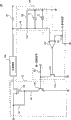
请参照图4,其是示出公知的一种照明系统的电路方块图。此照明系统400包括驱动装置406、光源模块408。而此照明系统400通过整流器404接收交流电源402所提供的交流电压。驱动装置406包括开关单元412、回授单元416、控制单元418、时序同步单元420以及亮度控制装置422。Please refer to FIG. 4 , which is a circuit block diagram of a known lighting system. The
时序同步单元420将所接收的交流电压转换成时序同步信号。控制单元418耦接至时序同步单元420,并依据时序同步信号的时序输出调整信号至开关单元412。开关单元412耦接于整流器404与光源模块408之间。当开关单元412接收到此调整信号后,会依据调整信号的状态(即逻辑高电平或逻辑低电平)来决定是否将交流电压提供给光源模块408,以使光源模块408产生光源。回授单元416耦接于光源模块408与控制单元418之间,并检测光源模块408的负载状态(例如是光源模块408的电流值),再依据检测结果输出回授信号至控制单元418。The
当控制单元418接收回授信号后,会先自亮度控制装置422中取得一预设亮度值。此预设亮度值可由使用者视需求自行调整。之后,控制单元418则将回授信号与预设亮度值作比对,以作为调整信号的脉宽的依据。When the
发明内容 Contents of the invention
本发明的目的是提供一种发光二极管驱动装置以及照明系统,其可根据光源模块的负载状态来决定是否断开光源模块与交流电源之间的连结。The object of the present invention is to provide an LED driving device and a lighting system, which can determine whether to disconnect the light source module from the AC power supply according to the load status of the light source module.
本发明的目的是提供一种发光二极管驱动装置以及照明系统,其可根据光源模块的负载状态以及光源模块的目前亮度来决定是否断开光源模块与交流电源之间的连结。The object of the present invention is to provide an LED driving device and a lighting system, which can decide whether to disconnect the light source module from the AC power supply according to the load status of the light source module and the current brightness of the light source module.
本发明提出一种发光二极管驱动装置,其电性耦接至一交流电源与一光源模块,且此交流电源输出一交流电压。此发光二极管驱动装置包括整流器、回授单元、保护单元、开关单元、时序单元以及控制单元。上述整流器电性耦接至交流电源与光源模块,以将交流电压提供给光源模块。上述回授单元电性耦接至光源模块,以检测及根据光源模块的负载状态产生一回授信号,并输出回授信号。上述保护单元电性耦接至回授单元,且接收回授信号,且将回授信号与保护单元内建的参考电压相比较,并输出一切换信号。上述开关单元具有第一端、第二端与第三端,开关单元的第一端电性耦接至交流电源,开关单元的第二端电性耦接至光源模块,开关单元的第三端电性耦接至保护单元,并接收及根据切换信号以连接或断开交流电源与光源模块的连结。上述时序单元电性耦接至交流电源,并撷取及对交流电压作一同步运算,以输出一时序同步信号。上述控制单元电性耦接至该时序单元与该保护单元,并接收及对该时序同步信号作一调整运算,用以输出一时序调整信号。The invention provides a LED driving device, which is electrically coupled to an AC power source and a light source module, and the AC power source outputs an AC voltage. The LED driving device includes a rectifier, a feedback unit, a protection unit, a switch unit, a timing unit and a control unit. The rectifier is electrically coupled to the AC power supply and the light source module to provide the AC voltage to the light source module. The feedback unit is electrically coupled to the light source module to detect and generate a feedback signal according to the load status of the light source module, and output the feedback signal. The protection unit is electrically coupled to the feedback unit, and receives the feedback signal, compares the feedback signal with a built-in reference voltage of the protection unit, and outputs a switching signal. The switch unit has a first end, a second end and a third end, the first end of the switch unit is electrically coupled to the AC power supply, the second end of the switch unit is electrically coupled to the light source module, and the third end of the switch unit It is electrically coupled to the protection unit, and receives and connects or disconnects the connection between the AC power supply and the light source module according to the switching signal. The timing unit is electrically coupled to the AC power supply, and captures and performs a synchronous operation on the AC voltage to output a timing synchronization signal. The control unit is electrically coupled to the timing unit and the protection unit, and receives and performs an adjustment operation on the timing synchronization signal to output a timing adjustment signal.
如本发明的优选实施例所述,保护单元接收一参考电压与一第二控制信号。此保护单元包括比较器、第一晶体管、第三电阻。上述比较器具有第一输入端、第二输入端以及输出端,比较器的第一输入端接收该回授信号,比较器的第二输入端接收该参考电压。上述第三电阻具有第一端与第二端,第三电阻的第一端接收第一控制信号。上述第一晶体管具有射极端、基极端以及集电极端,第一晶体管的集电极端电性耦接至第三电阻的第二端,第一晶体管的基极端电性耦接至比较器的输出端,第一晶体管的射极端电性耦接至地。。According to the preferred embodiment of the present invention, the protection unit receives a reference voltage and a second control signal. The protection unit includes a comparator, a first transistor, and a third resistor. The comparator has a first input terminal, a second input terminal and an output terminal, the first input terminal of the comparator receives the feedback signal, and the second input terminal of the comparator receives the reference voltage. The third resistor has a first terminal and a second terminal, and the first terminal of the third resistor receives the first control signal. The above-mentioned first transistor has an emitter terminal, a base terminal and a collector terminal, the collector terminal of the first transistor is electrically coupled to the second terminal of the third resistor, and the base terminal of the first transistor is electrically coupled to the output of the comparator terminal, and the emitter terminal of the first transistor is electrically coupled to the ground. .
本发明还提出一种发光二极管驱动装置,其电性耦接至交流电源与光源模块,且交流电源输出交流电压。此发光二极管驱动装置包括整流器、回授单元、保护单元以及开关单元。上述整流器电性耦接至交流电源与光源模块,以将交流电压提供给光源模块。上述回授单元电性耦接至光源模块,以检测及根据光源模块的负载状态产生回授信号,并输出回授信号。上述保护单元电性耦接至回授单元,且接收回授信号,用以将回授信号与保护单元内建的参考电压相比,并输出一切换信号。上述开关单元具有第一端、第二端与第三端,开关单元第一端电性耦接至交流电源,开关单元第二端电性耦接至光源模块,开关单元第三端电性耦接至保护单元,并接收及根据切换信号用以连接或断开交流电源与光源模块的连结。The present invention also provides a light emitting diode driving device, which is electrically coupled to an AC power source and a light source module, and the AC power source outputs an AC voltage. The LED driving device includes a rectifier, a feedback unit, a protection unit and a switch unit. The rectifier is electrically coupled to the AC power supply and the light source module to provide the AC voltage to the light source module. The above-mentioned feedback unit is electrically coupled to the light source module to detect and generate a feedback signal according to the load state of the light source module, and output the feedback signal. The protection unit is electrically coupled to the feedback unit, and receives the feedback signal, and compares the feedback signal with a built-in reference voltage of the protection unit, and outputs a switching signal. The above switch unit has a first end, a second end and a third end, the first end of the switch unit is electrically coupled to the AC power supply, the second end of the switch unit is electrically coupled to the light source module, and the third end of the switch unit is electrically coupled It is connected to the protection unit, and is used to connect or disconnect the AC power supply and the light source module according to the switching signal.
如本发明的优选实施例所述,保护单元接收参考电压与回授信号,且保护单元包括一比较器。此比较器具有第一输入端、第二输入端以及输出端,比较器的第一输入端电性耦接至回授单元,并接收回授信号,比较器的第二输入端接收参考电压。According to the preferred embodiment of the present invention, the protection unit receives the reference voltage and the feedback signal, and the protection unit includes a comparator. The comparator has a first input terminal, a second input terminal and an output terminal. The first input terminal of the comparator is electrically coupled to the feedback unit and receives the feedback signal. The second input terminal of the comparator receives the reference voltage.
本发明还提出一种发光二极管驱动装置,其电性耦接至交流电源与光源模块,且交流电源输出交流电压。此发光二极管驱动装置包括整流器、回授单元、控制单元、保护单元以及开关单元。上述整流器电性耦接至交流电源与光源模块,以将交流电压提供给光源模块。上述回授单元电性耦接至光源模块,以检测及根据光源模块的负载状态产生回授信号,并输出回授信号。上述控制单元电性耦接至回授单元,并接收及输出回授信号,且控制单元将回授信号与一预设亮度值作比较,以产生第一比较结果。上述保护单元电性耦接至控制单元,并接收回授信号以及第一比较结果,保护单元将回授信号与参考电压相比,以产生第二比较结果,保护单元则根据第一及第二比较结果,以产生及输出一切换信号。上述开关单元具有第一端、第二端与第三端,开关单元的第一端电性耦接至交流电源,开关单元的第二端电性耦接至光源模块,开关单元的第三端电性耦接至保护单元,并接收及根据切换信号用以连接或断开交流电源与光源模块的连结。The present invention also provides a light emitting diode driving device, which is electrically coupled to an AC power source and a light source module, and the AC power source outputs an AC voltage. The LED driving device includes a rectifier, a feedback unit, a control unit, a protection unit and a switch unit. The rectifier is electrically coupled to the AC power supply and the light source module to provide the AC voltage to the light source module. The above-mentioned feedback unit is electrically coupled to the light source module to detect and generate a feedback signal according to the load state of the light source module, and output the feedback signal. The control unit is electrically coupled to the feedback unit, and receives and outputs the feedback signal, and the control unit compares the feedback signal with a preset brightness value to generate a first comparison result. The protection unit is electrically coupled to the control unit and receives the feedback signal and the first comparison result. The protection unit compares the feedback signal with the reference voltage to generate a second comparison result, and the protection unit uses the first and second comparison results. The comparison result is used to generate and output a switching signal. The switch unit has a first end, a second end and a third end, the first end of the switch unit is electrically coupled to the AC power supply, the second end of the switch unit is electrically coupled to the light source module, and the third end of the switch unit It is electrically coupled to the protection unit, and is used to connect or disconnect the AC power supply and the light source module according to the switching signal.
本发明还提出一种照明系统,其电性耦接至交流电源,且交流电源输出交流电压。光源系统包括光源模块以及发光二极管驱动装置。上述光源模块电性耦接至交流电源,以接收交流电压。上述发光二极管驱动装置电性耦接至交流电源与光源模块,且包括整流器、回授单元、保护单元以及开关单元。其中,整流器电性耦接至交流电源与光源模块,以将交流电压提供给光源模块。回授单元电性耦接至光源模块,以检测及根据光源模块的负载状态产生回授信号,并输出回授信号。保护单元电性耦接至回授单元,且接收回授信号,用以将回授信号与保护单元内建的参考电压相比,并输出一切换信号。开关单元具有第一端、第二端与第三端,开关单元的第一端电性耦接至交流电源,开关单元的第二端电性耦接至光源模块,开关单元的第三端电性耦接至保护单元,并接收及根据切换信号用以连接或断开交流电源与光源模块的连结。The invention also provides a lighting system, which is electrically coupled to an AC power supply, and the AC power supply outputs an AC voltage. The light source system includes a light source module and an LED driving device. The above-mentioned light source module is electrically coupled to an AC power source to receive an AC voltage. The LED driving device is electrically coupled to the AC power supply and the light source module, and includes a rectifier, a feedback unit, a protection unit, and a switch unit. Wherein, the rectifier is electrically coupled to the AC power supply and the light source module to provide the AC voltage to the light source module. The feedback unit is electrically coupled to the light source module to detect and generate a feedback signal according to the load state of the light source module, and output the feedback signal. The protection unit is electrically coupled to the feedback unit, receives the feedback signal, compares the feedback signal with a built-in reference voltage of the protection unit, and outputs a switching signal. The switch unit has a first terminal, a second terminal and a third terminal, the first terminal of the switch unit is electrically coupled to the AC power supply, the second terminal of the switch unit is electrically coupled to the light source module, and the third terminal of the switch unit is electrically is coupled to the protection unit, and is used to connect or disconnect the AC power supply and the light source module according to the switching signal.
为使本发明的上述和其它目的、特征和优点能更明显易懂,下文特举一优选实施例,并配合附图,作详细说明如下。In order to make the above and other objects, features and advantages of the present invention more comprehensible, a preferred embodiment is exemplified below and described in detail with accompanying drawings.
附图说明 Description of drawings
图1A是示出依照本发明一优选实施例的一种照明系统的电路方块图;Fig. 1A is a circuit block diagram showing a lighting system according to a preferred embodiment of the present invention;
图1B是示出依照本发明一优选实施例的一种照明系统的部分详细电路图;Fig. 1B is a partial detailed circuit diagram showing a lighting system according to a preferred embodiment of the present invention;
图2是示出依照本发明另一优选实施例的一种照明系统的电路方块图;Fig. 2 is a circuit block diagram showing a lighting system according to another preferred embodiment of the present invention;
图3A是示出依照本发明再一优选实施例的一种照明系统的电路方块图;Fig. 3A is a circuit block diagram showing a lighting system according to yet another preferred embodiment of the present invention;
图3B是示出依照本发明再一优选实施例的一种照明系统的部分电路图;Fig. 3B is a partial circuit diagram showing a lighting system according to yet another preferred embodiment of the present invention;
图4是公知的一种照明系统的电路方块图;Fig. 4 is a circuit block diagram of a known lighting system;
图5A是示出依照本发明又一优选实施例的一种照明系统的电路方块图;Fig. 5A is a circuit block diagram showing a lighting system according to yet another preferred embodiment of the present invention;
图5B是示出依照本发明又一优选实施例的一种照明系统的部分电路图。Fig. 5B is a partial circuit diagram showing a lighting system according to yet another preferred embodiment of the present invention.
具体实施方式 Detailed ways
请参照图1A,其是示出依照本发明一优选实施例的一种照明系统的电路方块图。此照明系统100包括发光二极管驱动装置106以及光源模块108。Please refer to FIG. 1A , which is a circuit block diagram illustrating a lighting system according to a preferred embodiment of the present invention. The
在本发明的优选实施例中,光源模块108例如是发光二极管阵列或是单一的发光二极管,其数量应当不限于此。另外,发光二极管可以例如是由直流电压所驱动的发光二极管或是由交流电压所驱动的发光二极管。In a preferred embodiment of the present invention, the
此发光二极管驱动装置106包括整流器104、开关单元112、保护单元114、回授单元116、控制单元118以及时序单元120。在本实施例中,回授单元116电性耦接至光源模块108与保护单元114,以检测及根据光源模块108的一负载状态产生一回授信号,并输出回授信号。其中,此回授信号例如是流经光源模块108的电流值。The
其中,整流器104电性耦接至交流电源102,并接收一交流电压,用以在整流过后输出交流电压。而如本领域技术人员可轻易知晓的那样,整流器104可以例如不需要配置、被包含在发光二极管驱动装置106之内或之外,其应当视设计时的需求而定。Wherein, the
保护单元114接收回授单元116所传来的回授信号,并将回授信号与保护单元114内建的参考电压相比较。接着,根据比较结果输出一切换信号至开关单元112。其中,若回授信号所代表的电流值大于参考电压,则可以例如输出逻辑低电平(或逻辑高电平)的信号,以断开交流电源102与光源模块108间的电性连结;反之,若回授信号所代表的电流值小于参考电压,则可以例如输出逻辑高电平(或逻辑低电平)的信号,以连接或保持交流电源102与光源模块108间的电性连结。The
开关单元112具有第一端、第二端与第三端。开关单元112的第一端电性耦接至交流电源102(通过整流器104),开关单元112的第二端电性耦接至光源模块108,开关单元112的第三端电性耦接至保护单元114,并接收及根据切换信号用以连接或断开交流电源102与光源模块108的连结。The
时序单元120电性耦接至交流电源102(通过整流器104),并根据一预设周期撷取整流器104所输出的交流电压。其次,时序单元120将对所撷取到的交流电压作一同步运算,并产生及输出一时序同步信号。其中,时序同步信号欲使光源模块108工作周期与交流电压的周期能匹配。The
控制单元118电性耦接至时序单元120与保护单元114,并接收及对时序同步信号作一调整运算,以输出一时序调整信号。The
其中,开关单元112接收到时序调整信号时,则根据时序调整信号的电平决定断开整流器104与光源模块108的电性连结的时序,以调整提供给光源模块108的交流电压的脉宽。Wherein, when the
整流器104为对交流电源102所传来的交流电压作定电压与滤波后输出,以使光源模块108可以在更为稳定的电压下工作。其中,整流器104可以例如是桥式整流器,但不限于此。The
请继续参照图1A,此照明系统的操作方法为整流器104接收及对交流电源102所供给的交流电压作滤波整流后输出。光源模块108则根据开关单元112是否已与交流电源102(通过整流器104)作电性连结。若是,则交流电源102-整流器104-开关单元112-光源模块108-整流器104-交流电源102将形成一回路,故只要交流电压足以驱动光源模块108,光源模块108就将发光。Please continue to refer to FIG. 1A , the operation method of the lighting system is that the
此时,当光源模块108被驱动后,回授单元116将可测得光源模块108的回授电流值,并将回授电流值所相对应的回授信号输出至保护单元114。保护单元114则将此回授信号与内建的参考电压相比较,并输出一切换信号至开关单元112。接着,开关单元112则根据此切换信号决定是否切断光源模块108至交流电源102间的回路。另外,时序单元120则撷取及根据整流器104所输出的交流电压,并于进行同步运算后,输出时序同步信号至控制单元118。控制单元118则根据时序同步信号作调整运算,并通过保护单元114来控制开关单元112的开关,以调整提供给光源模块108的交流电压的脉宽。At this time, when the
请参照图1B,其是示出依照本发明一优选实施例的一种照明系统的部分详细电路图。在本实施例中,第七电阻R7具有第一端与第二端。第七电阻R7的第一端电性耦接至光源模块108,第七电阻R7的第二端电性耦接至整流器104。Please refer to FIG. 1B , which is a partial detailed circuit diagram of a lighting system according to a preferred embodiment of the present invention. In this embodiment, the seventh resistor R7 has a first terminal and a second terminal. A first end of the seventh resistor R7 is electrically coupled to the
此回授单元116包括第五电阻R5、第六电阻R6、电容C1以及二极管D1。此第五电阻R5具有第一端与第二端。第五电阻R5的第一端电性耦接至光源模块108,第五电阻R5的第二端电性耦接至保护单元114的比较器132的第一输入端。The
第六电阻R6具有第一端与第二端。第六电阻R6的第一端电性耦接至第五电阻R5的第二端,第六电阻R6的第二端电性耦接至地。The sixth resistor R6 has a first terminal and a second terminal. The first terminal of the sixth resistor R6 is electrically coupled to the second terminal of the fifth resistor R5, and the second terminal of the sixth resistor R6 is electrically coupled to the ground.
电容C1具有第一端与第二端。电容C1的第一端电性耦接至第五电阻R5的第二端,C1电容的第二端电性耦接至地。二极管D1具有第一端与第二端。The capacitor C1 has a first terminal and a second terminal. The first end of the capacitor C1 is electrically coupled to the second end of the fifth resistor R5, and the second end of the capacitor C1 is electrically coupled to the ground. The diode D1 has a first terminal and a second terminal.
二极管D1的第一端电性耦接至第五电阻R5的第二端,二极管D1的第二端电性耦接至地。The first end of the diode D1 is electrically coupled to the second end of the fifth resistor R5, and the second end of the diode D1 is electrically coupled to the ground.
其中,交流电压流经第五电阻R5之后,从第五电阻R5的第二端接回授信号传送至保护单元114的比较器132的第一输入端。Wherein, after the AC voltage flows through the fifth resistor R5 , the feedback signal from the second terminal of the fifth resistor R5 is transmitted to the first input terminal of the
保护单元114接收参考电压、第一控制信号与回授信号。保护单元114包括比较器132、第一晶体管134、第三电阻R3以及可变电阻140。其中,比较器132具有第一输入端、第二输入端以及输出端。比较器132的第一输入端电性耦接至回授单元116的第五电阻R5的第二端,并接收回授信号。比较器132的第二输入端接收一参考电压。比较器132则将参考电压与回授信号作比较,并根据比较结果输出一比较信号至第一晶体管134。The
如本领域技术人员可轻易知晓的那样,参考电压可以例如由一参考电压源所提供,而此参考电压等同于上述的参考电压。As those skilled in the art can easily understand, the reference voltage can be provided by, for example, a reference voltage source, and the reference voltage is equal to the above-mentioned reference voltage.
可变电阻140电性耦接于比较器132的第二输入端与参考电压的来源间。其中,可变电阻140使得使用者可根据实际需要来调整参考电压值。当然,可变电阻140的可调整范围所影响的交流电压大小必须是在光源模块108可承受的范围之内。The
第一晶体管134具有射极端、基极端以及集电极端。第一晶体管134的基极端电性耦接至比较器132的输出端,第一晶体管134的射极端电性耦接至地,第一晶体管134的集电极端电性耦接至开关单元112。The
第三电阻R3具有第一端与第二端。第三电阻R3的第一端接收第一控制信号,第三电阻R3的第二端电性耦接至第一晶体管134的集电极端与第二晶体管136的基极端。The third resistor R3 has a first terminal and a second terminal. A first terminal of the third resistor R3 receives the first control signal, and a second terminal of the third resistor R3 is electrically coupled to the collector terminal of the
其中,第一晶体管134则根据比较器132输出的比较信号决定是否被导通,并以此决定第一晶体管134的集电极端的电位。Wherein, the
在本发明的优选实施例中,第一晶体管134可以例如是双极性晶体管,但不限于此。第一控制信号可以例如是控制单元118所传来的控制信号。请继续参照图1B,开关单元112接收第一控制信号。此开关单包括第三晶体管138、第一电阻R1、第二电阻R2、第二晶体管136以及第三电阻R3。第三晶体管138具有漏极端、栅极端与源极端,第三晶体管138的漏极端电性耦接至光源模块108,第三晶体管138的源极端电性耦接至交流电源102(通过整流器104)。In a preferred embodiment of the present invention, the
在本实施例中,第一电阻R1具有第一端与第二端。第一电阻R1的第一端电性耦接至第三晶体管138的栅极端,第一电阻R1的第二端电性耦接至第三晶体管138的源极端。第二电阻R2具有第一端与第二端。第二电阻R2的第一端电性耦接至第三晶体管138的栅极端,第二电阻R2的第二端电性耦接至第二晶体管136的集电极端。In this embodiment, the first resistor R1 has a first terminal and a second terminal. The first terminal of the first resistor R1 is electrically coupled to the gate terminal of the
第二晶体管136具有射极端、基极端以及集电极端。第二晶体管136的射极端电性耦接至地。其中,第二晶体管136根据第一晶体管134的集电极端的电位决定是否被导通,即,当第一晶体管134未被导通时,第一晶体管134的集电极端的电位则由第一控制信号所决定;反之,当第一晶体管134被导通时,第一晶体管134的集电极端的电位则为逻辑低电平。The
其次,第三晶体管138则根据第二晶体管136的集电极端的电位决定是否被导通。Secondly, whether the
在本发明的优选实施例中,第二晶体管136可以例如是双极性晶体管,而第三晶体管可以例如是P型金属氧化物半导体,但均不限于此。In a preferred embodiment of the present invention, the
请参照图2,其是示出依照本发明另一优选实施例的一种照明系统的电路方块图。图2与图1A不同之处在于图2的回授单元电性耦接至控制单元118与光源模块108。此照明系统200包括发光二极管驱动装置206以及光源模块108。Please refer to FIG. 2 , which is a circuit block diagram illustrating a lighting system according to another preferred embodiment of the present invention. The difference between FIG. 2 and FIG. 1A is that the feedback unit in FIG. 2 is electrically coupled to the
在本发明的优选实施例中,光源模块108例如是发光二极管阵列或是单一的发光二极管,其数量应当不限于此。In a preferred embodiment of the present invention, the
此发光二极管驱动装置206包括整流器104、开关单元112、保护单元114、回授单元116、控制单元118以及时序单元120。在本实施例中,回授单元116电性耦接至光源模块108与控制单元118,以检测及根据光源模块108的一负载状态产生一回授信号,并输出回授信号。其中,此回授信号例如是流经光源模块108的电流值。The
其中,整流器104电性耦接至交流电源102,并接收一交流电压,用以在整流过后输出交流电压。而如本领域技术人员可轻易知晓的那样,整流器104可以例如不需要配置、被包含在照明系统200之内或之外,其应当视设计时的需求而定。Wherein, the
时序单元120电性耦接至交流电源102(通过整流器104),并根据一预设周期撷取整流器104所输出的交流电压。其次,时序单元120将对所撷取到的交流电压作一同步运算,并产生及输出一时序同步信号。其中,时序同步信号欲使光源模块108工作周期与交流电压的周期能匹配。The
控制单元118电性耦接至时序单元120与回授单元116。控制单元118接收回授单元116所传来的回授信号,并接收及输出回授信号。其中,控制单元118将此回授信号与一预设亮度值相比,并得到第一比较结果。如本领域技术人员可以轻易知晓的那样,预设亮度值可以例如储存于控制单元118芯片内的内存或与控制单元118芯片相连接的内存。The
另外,控制单元118还接收时序单元120所传来的时序同步信号,并对时序同步信号作一调整运算,以通过保护单元114输出一时序调整信号。In addition, the
保护单元114电性耦接至控制单元118,并接收回授信号。保护单元114将回授信号与保护单元114内建的参考电压相比较,并得到第二比较结果。接着,根据第一及第二比较结果输出一切换信号至开关单元112。其中,若回授信号所代表的电流值大于参考电压,则可以例如输出逻辑低电平(或逻辑高电平)的信号,以断开交流电源102与光源模块108间的电性连结;反之,若回授信号所代表的电流值小于参考电压,则可以例如输出逻辑高电平(或逻辑低电平)的信号,以连接或保持交流电源102与光源模块108间的电性连结。The
在本发明的优选实施例中,若回授信号比预设亮度值大,则代表第一比较结果的切换信号为调窄交流电压的脉宽;反之,若回授信号比预设亮度值小,则代表第一比较结果的切换信号为调大交流电压的脉宽。In a preferred embodiment of the present invention, if the feedback signal is larger than the preset brightness value, the switching signal representing the first comparison result is to narrow the pulse width of the AC voltage; otherwise, if the feedback signal is smaller than the preset brightness value , the switching signal representing the first comparison result is to increase the pulse width of the AC voltage.
开关单元112具有第一端、第二端与第三端。开关单元112的第一端电性耦接至交流电源102(通过整流器104),开关单元112的第二端电性耦接至光源模块108,开关单元112的第三端电性耦接至保护单元114,并接收及根据切换信号用以连接或断开交流电源102与光源模块108的连结。The
其中,开关单元112接收到时序调整信号时,则根据时序调整信号的电平决定断开整流器104与光源模块108的电性连结的时序,以调整提供给光源模块108的交流电压的脉宽。Wherein, when the
在本发明的优选实施例中,当第一比较结果与第二比较结果其中之一表示需要调整开关单元112的开关周期时,保护单元114所输出的切换信号即对开关单元112的开关周期作调整。In a preferred embodiment of the present invention, when one of the first comparison result and the second comparison result indicates that the switching period of the
整流器104为对交流电源102所传来的交流电压作定电压与滤波后输出,以使光源模块108可以在更为稳定的电压下工作。其中,整流器104可以例如是桥式整流器,但不限于此。The
请继续参照图2,此照明系统的操作方法为整流器104接收及对交流电源102所提供的交流电压作滤波整流后输出。光源模块108则根据开关单元112是否已与交流电源102(通过整流器104)作电性连结。若是,则交流电源102-整流器104-开关单元112-光源模块108-整流器104-交流电源102将形成一回路,故只要交流电压足以驱动光源模块108,光源模块108就将发光。Please continue to refer to FIG. 2 , the operation method of the lighting system is that the
此时,当光源模块108被驱动后,回授单元116将可测得光源模块108的回授电流值,并将回授电流值所相对应的回授信号输出至控制单元118与保护单元114(通过控制单元118)。控制单元118则将回授信号与预设亮度值相比,并得到及输出第一比较结果。保护单元114则将此回授信号与内建的参考电压相比较,并得到第二比较结果。其次,保护单元114根据第一比较结果与第二比较结果产生及输出一切换信号至开关单元112。接着,开关单元112则根据此切换信号决定是否切断光源模块108至交流电源102间的回路。另外,时序单元120则撷取及根据整流器104所输出的交流电压,并于进行同步运算后,输出时序同步信号至控制单元118。控制单元118则根据时序同步信号作调整运算,并通过保护单元114来控制开关单元112的开关,以调整提供给光源模块108的交流电压的脉宽。At this time, when the
在本发明的优选实施例中,由于图2的详细电路图与图1B大致类似,故在此不再赘述。In a preferred embodiment of the present invention, since the detailed circuit diagram of FIG. 2 is substantially similar to that of FIG. 1B , details are not repeated here.
接着请参照图3A,其是示出依照本发明再一优选实施例的一种照明系统的电路方块图。图3A与图1A的不同之处在于图3A没有控制单元118与时序单元120。此照明系统300包括系包括发光二极管驱动装置306以及光源模块108。Next, please refer to FIG. 3A , which is a circuit block diagram illustrating a lighting system according to yet another preferred embodiment of the present invention. The difference between FIG. 3A and FIG. 1A is that FIG. 3A does not have the
在本发明的优选实施例中,光源模块108例如是发光二极管阵列或是单一的发光二极管,其数量应当不限于此。In a preferred embodiment of the present invention, the
此发光二极管驱动装置306包括整流器104、开关单元112、保护单元114、回授单元116。在本实施例中,回授单元116电性耦接至光源模块108与保护单元114,以检测及根据光源模块108的一负载状态产生一回授信号,并输出回授信号。其中,此回授信号例如是流经光源模块108的电流值。The LED driving device 306 includes a
其中,整流器104电性耦接至交流电源102,并接收一交流电压,用以在整流过后输出交流电压。而如本领域技术人员可轻易知晓的那样,整流器104可以例如不需要配置、被包含在照明系统300之内或之外,其应当视设计时的需求而定。Wherein, the
保护单元114接收回授单元116所传来的回授信号,并将回授信号与保护单元114内建的参考电压相比较。接着,根据比较结果输出一切换信号至开关单元112。其中,若回授信号所代表的电流值大于参考电压,则可以例如输出逻辑低电平(或逻辑高电平)的信号,以断开交流电源102与光源模块108间的电性连结;反之,若回授信号所代表的电流值小于参考电压,则可以例如输出逻辑高电平(或逻辑低电平)的信号,以连接或保持交流电源102与光源模块108间的电性连结。The
开关单元112具有第一端、第二端与第三端。开关单元112的第一端电性耦接至交流电源102(通过整流器104),开关单元112的第二端电性耦接至光源模块108,开关单元112的第三端电性耦接至保护单元114,并接收及根据切换信号用以连接或断开交流电源102与光源模块108的连结。The
整流器104为对交流电源102所传来的交流电压作定电压与滤波后输出,以使光源模块108可以在更为稳定的电压下工作。其中,整流器104可以例如是桥式整流器,但不限于此。The
请继续参照图3A,此照明系统的操作方法为整流器104接收及对交流电源102所供给的交流电压作滤波整流后输出。光源模块108则根据开关单元112是否已与交流电源102(通过整流器104)作电性连结。若是,则交流电源102-整流器104-开关单元112-光源模块108-整流器104-交流电源102将形成一回路,故只要交流电压足以驱动光源模块108,光源模块108就将发光。Please continue to refer to FIG. 3A , the operation method of the lighting system is that the
此时,当光源模块108被驱动后,回授单元116将可测得光源模块108的回授电流值,并将回授电流值所相对应的回授信号输出至保护单元114。保护单元114则将此回授信号与内建的参考电压相比较,并输出一切换信号至开关单元112。接着,开关单元112则根据此切换信号决定是否切断光源模块108至交流电源102间的回路。At this time, when the
请参照图3B,其是示出依照本发明一优选实施例的一种照明系统的部分详细电路图。在本实施例中,第七电阻R7具有第一端与第二端。第七电阻R7的第一端电性耦接至光源模块108,第七电阻R7的第二端电性耦接至整流器104。Please refer to FIG. 3B , which is a partial detailed circuit diagram of a lighting system according to a preferred embodiment of the present invention. In this embodiment, the seventh resistor R7 has a first terminal and a second terminal. A first end of the seventh resistor R7 is electrically coupled to the
此回授单元116包括第五电阻R5、第六电阻R6、电容C1以及二极管D1。此第五电阻R5具有第一端与第二端。第五电阻R5的第一端电性耦接至光源模块108,第五电阻R5的第二端电性耦接至保护单元114的比较器132的第一输入端。The
第六电阻R6具有第一端与第二端。第六电阻R6的第一端电性耦接至第五电阻R5的第二端,第六电阻R6的第二端电性耦接至地。The sixth resistor R6 has a first terminal and a second terminal. The first terminal of the sixth resistor R6 is electrically coupled to the second terminal of the fifth resistor R5, and the second terminal of the sixth resistor R6 is electrically coupled to the ground.
电容C1具有第一端与第二端。电容C1的第一端电性耦接至第五电阻R5的第二端,C1电容的第二端电性耦接至地。二极管D1具有第一端与第二端。The capacitor C1 has a first terminal and a second terminal. The first end of the capacitor C1 is electrically coupled to the second end of the fifth resistor R5, and the second end of the capacitor C1 is electrically coupled to the ground. The diode D1 has a first terminal and a second terminal.
二极管D1的第一端电性耦接至第五电阻R5的第二端,二极管D1的第二端电性耦接至地。The first end of the diode D1 is electrically coupled to the second end of the fifth resistor R5, and the second end of the diode D1 is electrically coupled to the ground.
其中,交流电压流经第五电阻R5之后,从第五电阻R5的第二端接回授信号传送至保护单元114的比较器132的第一输入端。Wherein, after the AC voltage flows through the fifth resistor R5 , the feedback signal from the second terminal of the fifth resistor R5 is transmitted to the first input terminal of the
保护单元114接收参考电压与回授信号。保护单元114包括比较器132。其中,比较器132具有第一输入端、第二输入端以及输出端。比较器132的第一输入端电性耦接至回授单元116的第五电阻R5的第二端,并接收回授信号。比较器132的第二输入端接收一参考电压。比较器132则将参考电压与回授信号作比较,并根据比较结果输出一比较信号至开关单元112的第二晶体管136的基极端。如本领域技术人员可轻易知晓的那样,参考电压可以例如由一参考电压源所提供,而此参考电压等同于上述的参考电压。The
请继续参照图3B,开关单元112接收保护单元114的比较信号。此开关单包括第三晶体管138、第一电阻R1、第二电阻R2以及第二晶体管136。第三晶体管138具有漏极端、栅极端与源极端,第三晶体管138的漏极端电性耦接至光源模块108,第三晶体管138的源极端电性耦接至交流电源102(通过整流器104)。Please continue to refer to FIG. 3B , the
第二晶体管136具有射极端、基极端以及集电极端。第二晶体管136的射极端电性耦接至地,第二晶体管136的集电极端电性耦接至第三晶体管138的栅极端(通过第二电阻R2)。其中,第二晶体管136根据比较信号的电位决定是否被导通。The
在本实施例中,第一电阻R1具有第一端与第二端。第一电阻R1的第一端电性耦接至第三晶体管138的栅极端,第一电阻R1的第二端电性耦接至第三晶体管138的源极端。第二电阻R2具有第一端与第二端。第二电阻R2的第一端电性耦接至第三晶体管138的栅极端,第二电阻R2的第二端电性耦接至第二晶体管136的集电极端。In this embodiment, the first resistor R1 has a first terminal and a second terminal. The first terminal of the first resistor R1 is electrically coupled to the gate terminal of the
其次,第三晶体管138则根据第二晶体管136的集电极端的电位决定是否被导通。Secondly, whether the
请参照图5A,其是示出依照本发明又一优选实施例的一种照明系统的电路方块图。照明系统500包括发光二极管驱动装置506以及光源模块108。此光源模块108与前述的光源模块相同,故在此不再赘述。Please refer to FIG. 5A , which is a circuit block diagram illustrating a lighting system according to another preferred embodiment of the present invention. The
发光二极管驱动装置506电性耦接至交流电源102与光源模块108。发光二极管驱动装置506包括整流器104、第一回授单元106a、第二回授单元106b、开关单元112、保护单元114。The
在本实施例中,整流器104电性耦接至交流电源102与光源模块108,以将交流电压提供给光源模块108。In this embodiment, the
第一回授单元116a电性耦接至整流器104,以检测及根据整流器104输出的交流电压产生一第一回授信号,并输出第一回授信号。而第二回授单元116b电性耦接至光源模块108,以检测及根据光源模块108的一负载状态产生一第二回授信号,并输出第二回授信号。The
保护单元114电性耦接至第一回授单元116a与第二回授单元116b,且接收第一回授信号与第二回授信号。第一回授单元116a将第一回授信号与保护单元114内建的第一参考电压相比,第二回授单元116b将第二回授信号与保护单元114内建的第二参考电压相比,并选择性地输出一切换信号。The
开关单元112具有第一端、第二端与第三端。开关单元112的第一端电性耦接至交流电源102(通过整流器104),开关单元112的第二端电性耦接至光源模块108,开关单元112的第三端电性耦接至保护单元114。开关单元112接收及根据切换信号用以连接或断开交流电源102与光源模块108的连结(通过整流器104)。The
请参照图5B,其是示出依照本发明又一优选实施例的一种照明系统的部分电路图。此保护单元114接收第一及第二参考电压、第一及第二回授信号与第一控制信号。Please refer to FIG. 5B , which is a partial circuit diagram of a lighting system according to another preferred embodiment of the present invention. The
在本实施例中,由于第二回授单元116b、开关单元112的组成与功能分别与前述的回授单元116及开关单元112相同,故在此不再赘述。In this embodiment, since the components and functions of the
保护单元114包括第二比较器132、第三电阻R3、第一晶体管134、第一比较器152以及第四晶体管154。第二比较器132具有第一输入端、第二输入端以及输出端。第二比较器132的第一输入端电性耦接至第二回授单元116b,并接收第二回授信号。第二比较器132的第二输入端接收第二参考电压。其中,在第二比较器132的第二输入端与第二参考电压的来源间还配置有一可变电阻140。因此,被输入至第二比较器132的第二输入端的第二参考电压的值可根据可变电阻140的阻值而被调整。其中,第二比较器132将第二参考电压与第二回授信号作比较,以输出一第二比较信号。The
第三电阻R3具有第一端与第二端。此第三电阻R3的第一端接收一第一控制信号,第三电阻R3的第二端电性耦接至第一晶体管134的集电极端。其中,此第一控制信号可以例如是工作电压或控制信号(如果照明系统有配置控制单元的话),但不限于此。The third resistor R3 has a first terminal and a second terminal. The first terminal of the third resistor R3 receives a first control signal, and the second terminal of the third resistor R3 is electrically coupled to the collector terminal of the
第一晶体管134具有射极端、基极端以及集电极端。第一晶体管134的基极端电性耦接至第二比较器132的输出端,以接收第二比较信号。第一晶体管134的射极端电性耦接至地。其中,第一晶体管134根据第二比较信号的电位来决定是否导通。The
第一比较器152具有第一输入端、第二输入端以及输出端。第一比较器152的第一输入端电性耦接至第一回授单元166a,并接收第一回授信号。第一比较器152的第二输入端接收第一参考电压。其中,在第一比较器152的第二输入端与第一参考电压的来源间还配置有一可变电阻156。因此,被输入至第一比较器152的第二输入端的第一参考电压的值可根据可变电阻156的阻值而被调整。其中,第一比较器152将第二参考电压与第二回授信号作比较,以输出一第一比较信号。The
第四晶体管154具有射极端、基极端以及集电极端。第四晶体管154的射极端电性耦接至地,第四晶体管154的基极端电性耦接至第一比较器152的输出端,第四晶体管154的集电极端电性耦接至第三电阻R3的第二端。其中,第一比较器152将第一参考电压与第一回授信号作比较,以输出一第一比较信号。The
在本实施例中,第一回授单元116a包括第八电阻R8与第九电阻R9。其中,第八电阻R8具有第一端与第二端,第八电阻R8的第一端电性耦接至第三晶体管138的源极端,第八电阻R8的第二端电性耦接至第一比较器152的第一输入端。第九电阻R9具有第一端与第二端,第九电阻R9的第一端电性耦接至第八电阻R8的第二端,第九电阻R9的第二端电性耦接至地。In this embodiment, the
请继续参照图5B,此照明系统500的部分电路图的操作方法为当整流器输出的交流电压太大时,第一比较器152输出的第一比较信号将导通第四晶体管154,因此可以使第三电阻R3的第二端的电位为低电位。同样地,当第二回授单元116b监测到光源模块108的回授电压过大时,第二比较器132输出的第一比较信号将导通第一晶体管134,因此可以使第三电阻R3的第二端的电位为低电位。Please continue to refer to FIG. 5B. The operation method of the partial circuit diagram of the
接着,当第三电阻R3的第二端的电位为低电位时,第二晶体管136不会被导通,故第三晶体管138将不会被导通。所以,整流器104输出的交流电压将不会被提供给光源模块108。因此,如图5B的设计,将可在整流器104输出的交流电压或光源模块108的回授电压过大时,即关闭开关单元112,以保护照明系统。在本发明的优选实施例中,第三晶体管可以例如是P型金属氧化物半导体,但不以此为限。Next, when the potential of the second end of the third resistor R3 is low, the
在本发明之优选实施例中,照明系统100、200、300、500可以例如是单纯的照明系统或为显示装置的背光源,但均不限于此。In a preferred embodiment of the present invention, the
综合以上所述,本发明的驱动装置与照明系统,可在流经光源模块的电流值太大或是整流器输出的交流电压过大时,通过开关单元断开光源模块与交流电源之间的电性连结,以避免因电流太大而使光源模块被烧毁。增加此保护单元不但可以调整亮度值,还可保护光源模块。Based on the above, the driving device and lighting system of the present invention can cut off the power between the light source module and the AC power supply through the switch unit when the current value flowing through the light source module is too large or the AC voltage output by the rectifier is too large. Sexual connection to avoid the light source module being burned due to too much current. Adding this protection unit can not only adjust the brightness value, but also protect the light source module.
虽然本发明已以优选实施例披露如上,然其并非用以限定本发明,任何本领域技术人员,在不脱离本发明的精神和范围内,当可作些许的更动与润饰,因此本发明的保护范围当视所附的权利要求所限定的范围为准。Although the present invention has been disclosed above with preferred embodiments, it is not intended to limit the present invention. Any person skilled in the art may make some changes and modifications without departing from the spirit and scope of the present invention. Therefore, the present invention The scope of protection should be subject to the scope defined by the appended claims.
Claims (34)
Priority Applications (1)
| Application Number | Priority Date | Filing Date | Title |
|---|---|---|---|
| CN2008102159619A CN101674692B (en) | 2008-09-12 | 2008-09-12 | Light-emitting diode driving device and lighting system |
Applications Claiming Priority (1)
| Application Number | Priority Date | Filing Date | Title |
|---|---|---|---|
| CN2008102159619A CN101674692B (en) | 2008-09-12 | 2008-09-12 | Light-emitting diode driving device and lighting system |
Publications (2)
| Publication Number | Publication Date |
|---|---|
| CN101674692A true CN101674692A (en) | 2010-03-17 |
| CN101674692B CN101674692B (en) | 2013-07-10 |
Family
ID=42021604
Family Applications (1)
| Application Number | Title | Priority Date | Filing Date |
|---|---|---|---|
| CN2008102159619A Expired - Fee Related CN101674692B (en) | 2008-09-12 | 2008-09-12 | Light-emitting diode driving device and lighting system |
Country Status (1)
| Country | Link |
|---|---|
| CN (1) | CN101674692B (en) |
Cited By (3)
| Publication number | Priority date | Publication date | Assignee | Title |
|---|---|---|---|---|
| CN102892238A (en) * | 2012-10-30 | 2013-01-23 | 四川新力光源股份有限公司 | Dimming drive circuit of LED module directly driven by alternating current |
| WO2013097692A1 (en) * | 2011-12-31 | 2013-07-04 | 四川新力光源股份有限公司 | Alternating current direct drive led light-emitting device |
| CN104885570A (en) * | 2012-11-16 | 2015-09-02 | 首尔伟傲世有限公司 | Light-emitting diode driving device, driving method and light-emitting diode lighting module comprising same |
Family Cites Families (2)
| Publication number | Priority date | Publication date | Assignee | Title |
|---|---|---|---|---|
| KR100982167B1 (en) * | 2002-12-19 | 2010-09-14 | 코닌클리즈케 필립스 일렉트로닉스 엔.브이. | Power supply for LED light source and method of operating LED light source |
| CN100546424C (en) * | 2004-04-27 | 2009-09-30 | 厦门通士达照明有限公司 | A kind of electric ballast with the protection of dying of old age |
-
2008
- 2008-09-12 CN CN2008102159619A patent/CN101674692B/en not_active Expired - Fee Related
Cited By (5)
| Publication number | Priority date | Publication date | Assignee | Title |
|---|---|---|---|---|
| WO2013097692A1 (en) * | 2011-12-31 | 2013-07-04 | 四川新力光源股份有限公司 | Alternating current direct drive led light-emitting device |
| CN102892238A (en) * | 2012-10-30 | 2013-01-23 | 四川新力光源股份有限公司 | Dimming drive circuit of LED module directly driven by alternating current |
| CN102892238B (en) * | 2012-10-30 | 2015-02-04 | 四川新力光源股份有限公司 | Dimming drive circuit of LED module directly driven by alternating current |
| CN104885570A (en) * | 2012-11-16 | 2015-09-02 | 首尔伟傲世有限公司 | Light-emitting diode driving device, driving method and light-emitting diode lighting module comprising same |
| CN104885570B (en) * | 2012-11-16 | 2018-08-14 | 首尔伟傲世有限公司 | Light emitting diode drive device, driving method and light-emitting diode lighting module |
Also Published As
| Publication number | Publication date |
|---|---|
| CN101674692B (en) | 2013-07-10 |
Similar Documents
| Publication | Publication Date | Title |
|---|---|---|
| US8044603B2 (en) | Light emitting diode driving device and light system | |
| TWI423732B (en) | Lighting apparatus, driving circuit of light emitting diode and driving method using the same | |
| TWI448198B (en) | System and method for dimming control under capacitive loads | |
| JP4944658B2 (en) | LED drive circuit | |
| JP5003850B1 (en) | LED illuminator and LED illumination system | |
| JP4818350B2 (en) | Light emitting diode drive circuit | |
| US9456475B2 (en) | LED light source with reduced flicker | |
| JP2009021535A (en) | Light source device and its driving device | |
| US8981674B2 (en) | Detector circuit and method for operating a detector circuit | |
| TW201422045A (en) | High stability LED control circuit | |
| WO2015090186A1 (en) | Overvoltage and overcurrent protection circuit and electronic device | |
| US11602021B2 (en) | Linear drive circuit and led light having the same | |
| TW201352057A (en) | Load driving apparatus relating to LED lamp and method thereof and illumination apparatus using the same | |
| TW201332390A (en) | Flicker-free LED driver circuit with a high power factor | |
| TW201325302A (en) | LED driving device and method thereof | |
| TWI594664B (en) | Light-emitting diode driving device and short protection method for driving device | |
| JPH11307815A (en) | Collective led lamp for ac power source | |
| CN102065598B (en) | Lighting device, driving circuit of light-emitting diode and driving method thereof | |
| TWM501708U (en) | High stability LED control circuit | |
| CN105392231A (en) | System for providing output current for one or multiple LED | |
| KR101414902B1 (en) | AC LED driving circuit | |
| CN101674692B (en) | Light-emitting diode driving device and lighting system | |
| CN101222798B (en) | Driving circuit of light emitting diode | |
| CN102958240B (en) | Light source device and dimming control circuit thereof | |
| TW201712643A (en) | Traffic signal light drive circuit |
Legal Events
| Date | Code | Title | Description |
|---|---|---|---|
| C06 | Publication | ||
| PB01 | Publication | ||
| C10 | Entry into substantive examination | ||
| SE01 | Entry into force of request for substantive examination | ||
| C14 | Grant of patent or utility model | ||
| GR01 | Patent grant | ||
| CF01 | Termination of patent right due to non-payment of annual fee |
Granted publication date: 20130710 Termination date: 20200912 |
|
| CF01 | Termination of patent right due to non-payment of annual fee |