CN101673787B - Semiconductor light emitting device and packaging structure thereof - Google Patents
Semiconductor light emitting device and packaging structure thereof Download PDFInfo
- Publication number
- CN101673787B CN101673787B CN2008101494130A CN200810149413A CN101673787B CN 101673787 B CN101673787 B CN 101673787B CN 2008101494130 A CN2008101494130 A CN 2008101494130A CN 200810149413 A CN200810149413 A CN 200810149413A CN 101673787 B CN101673787 B CN 101673787B
- Authority
- CN
- China
- Prior art keywords
- transparent adhesive
- semiconductor light
- adhesive tape
- tape material
- light emitting
- Prior art date
- Legal status (The legal status is an assumption and is not a legal conclusion. Google has not performed a legal analysis and makes no representation as to the accuracy of the status listed.)
- Active
Links
Images


Classifications
-
- H—ELECTRICITY
- H10—SEMICONDUCTOR DEVICES; ELECTRIC SOLID-STATE DEVICES NOT OTHERWISE PROVIDED FOR
- H10H—INORGANIC LIGHT-EMITTING SEMICONDUCTOR DEVICES HAVING POTENTIAL BARRIERS
- H10H20/00—Individual inorganic light-emitting semiconductor devices having potential barriers, e.g. light-emitting diodes [LED]
- H10H20/80—Constructional details
- H10H20/85—Packages
- H10H20/851—Wavelength conversion means
-
- H—ELECTRICITY
- H10—SEMICONDUCTOR DEVICES; ELECTRIC SOLID-STATE DEVICES NOT OTHERWISE PROVIDED FOR
- H10H—INORGANIC LIGHT-EMITTING SEMICONDUCTOR DEVICES HAVING POTENTIAL BARRIERS
- H10H20/00—Individual inorganic light-emitting semiconductor devices having potential barriers, e.g. light-emitting diodes [LED]
- H10H20/80—Constructional details
- H10H20/85—Packages
- H10H20/852—Encapsulations
- H10H20/853—Encapsulations characterised by their shape
-
- H—ELECTRICITY
- H10—SEMICONDUCTOR DEVICES; ELECTRIC SOLID-STATE DEVICES NOT OTHERWISE PROVIDED FOR
- H10H—INORGANIC LIGHT-EMITTING SEMICONDUCTOR DEVICES HAVING POTENTIAL BARRIERS
- H10H20/00—Individual inorganic light-emitting semiconductor devices having potential barriers, e.g. light-emitting diodes [LED]
- H10H20/80—Constructional details
- H10H20/85—Packages
- H10H20/855—Optical field-shaping means, e.g. lenses
- H10H20/856—Reflecting means
Landscapes
- Led Device Packages (AREA)
- Led Devices (AREA)
Abstract
Description
技术领域 technical field
本发明涉及一种半导体发光装置及其封装结构,尤其关于一种具有波长转换结构及一透明胶材的半导体发光装置及其封装结构。The invention relates to a semiconductor light-emitting device and its packaging structure, in particular to a semiconductor light-emitting device with a wavelength conversion structure and a transparent adhesive material and its packaging structure.
背景技术 Background technique
发光二极管(Light-emitting Diode;LED)为一种半导体固态元件,至少包含一p-n结(p-n junction),此p-n结形成于p型与n型半导体层之间。当在p-n结上施加一定程度的偏压时,p型半导体层中的空穴与n型半导体层中的电子将会结合而释放出光。此光产生的区域一般又称为有源区(activeregion)。A light-emitting diode (Light-emitting Diode; LED) is a semiconductor solid-state device that includes at least one p-n junction (p-n junction), which is formed between p-type and n-type semiconductor layers. When a certain degree of bias is applied to the p-n junction, holes in the p-type semiconductor layer and electrons in the n-type semiconductor layer will combine to release light. The region where the light is generated is generally called an active region.
LED的主要特征在于尺寸小、发光效率高、寿命长、反应快速、可靠度高和色度良好,目前已经广泛使用在电器、汽车、招牌和交通号志上。随着全彩LED的问世,LED已逐渐取代如荧光灯和白热灯泡等传统照明设备。The main features of LEDs are small size, high luminous efficiency, long life, fast response, high reliability and good chromaticity, and have been widely used in electrical appliances, automobiles, signboards and traffic signals. With the advent of full-color LEDs, LEDs have gradually replaced traditional lighting equipment such as fluorescent lamps and incandescent bulbs.
一般是以LED裸芯搭配波长转换材料(如荧光粉)来产生白光,波长转换材料在被LED裸芯所发出的蓝光照射后会激发黄光、绿光或红光,将蓝光和黄光、绿光或红光混合之后即可产生白光。为了确使LED裸芯所发出的光可以通过波长转换材料并于混合后产生所需的光,波长转换材料必须完全地覆盖在LED裸芯可能出光之处。然而光所射出的方向没有特定方向,若波长转换材料没有完全地覆盖在LED裸芯可能出光之处,使部分光线未能通过波长转换材料,如边射的光,会导致光的波长转换效率降低。另一方面,若波长转换材料完全地包覆LED裸芯,虽可提高波长转换的效率,但是却容易造成散热不易等问题。Generally, white light is produced by pairing the bare LED core with a wavelength conversion material (such as phosphor powder). Mixing green or red light produces white light. In order to ensure that the light emitted by the bare LED core can pass through the wavelength conversion material and produce the required light after being mixed, the wavelength conversion material must completely cover the possible light emission of the LED core. However, there is no specific direction in which the light is emitted. If the wavelength conversion material does not completely cover the possible light emission of the LED core, part of the light fails to pass through the wavelength conversion material, such as side-ray light, which will lead to a decrease in the wavelength conversion efficiency of light. reduce. On the other hand, if the wavelength conversion material completely covers the bare LED core, although the efficiency of wavelength conversion can be improved, it will easily cause problems such as difficult heat dissipation.
将波长转换材料均匀地覆盖在LED裸芯上并不容易。当覆盖在LED裸芯上的波长转换材料厚度不均匀时,由于较厚的波长转换材料会比较薄的波长转换材料吸收较多的光,射向不同方向的光经过厚度相异的波长转换材料所激发出来的色光会因此有所差异。It is not easy to uniformly cover the wavelength conversion material on the LED die. When the thickness of the wavelength conversion material covering the bare LED core is not uniform, since the thicker wavelength conversion material absorbs more light than the thinner wavelength conversion material, the light emitted in different directions passes through the wavelength conversion material with different thickness The color light excited will be different accordingly.
发明内容 Contents of the invention
本发明提供一种半导体发光装置,其包含一导电基板、一半导体发光叠层、一透明胶材及一波长转换结构。半导体发光叠层所发的原色光透过透明胶材由波长转换结构转换后产生与原色光波长相异的变色光。此外,导电基板与半导体发光叠层之间更至少包含一反射层。The invention provides a semiconductor light-emitting device, which includes a conductive substrate, a semiconductor light-emitting stack, a transparent adhesive material and a wavelength conversion structure. The primary-color light emitted by the semiconductor light-emitting stack passes through the transparent adhesive material and is converted by the wavelength conversion structure to produce color-changing light with a wavelength different from that of the primary-color light. In addition, at least one reflective layer is included between the conductive substrate and the semiconductor light emitting stack.
本发明提供一种半导体发光装置,其包含一导电基板、一半导体发光叠层、一透明胶材、与均匀分布于透明胶材中的一波长转换材料。半导体发光叠层所发的原色光经过波长转换材料产生与原色光波长相异的变色光。此外,导电基板与半导体发光叠层之间更至少包含一反射层。The invention provides a semiconductor light-emitting device, which includes a conductive substrate, a semiconductor light-emitting stack, a transparent adhesive material, and a wavelength conversion material uniformly distributed in the transparent adhesive material. The primary color light emitted by the semiconductor light-emitting stack passes through the wavelength conversion material to produce color-changing light with a wavelength different from that of the primary color light. In addition, at least one reflective layer is included between the conductive substrate and the semiconductor light emitting stack.
本发明提供一种半导体发光装置,其包含一导电基板、一半导体发光叠层、一透明胶材、存在于透明胶材中的一波长转换结构。半导体发光叠层所发的原色光经过透明胶材后由波长转换结构转换产生与原色光波长相异的变色光。此外,导电基板与半导体发光叠层之间更至少包含一反射层。The invention provides a semiconductor light-emitting device, which includes a conductive substrate, a semiconductor light-emitting stack, a transparent adhesive material, and a wavelength conversion structure existing in the transparent adhesive material. The primary color light emitted by the semiconductor light-emitting stack passes through the transparent adhesive material and is converted by the wavelength conversion structure to produce color-changing light with a wavelength different from that of the primary color light. In addition, at least one reflective layer is included between the conductive substrate and the semiconductor light emitting stack.
本发明提供一种半导体发光装置封装结构,包含一半导体发光装置、一碗杯、一封装支架、一透明胶材及一波长转换结构。其中半导体发光装置置于碗杯中,将透明胶材充填于碗杯,其高度至少大于半导体发光装置高度,再将波长转换结构设置于透明胶材之上。此外,透明胶材与波长转换结构之间还至少包含一波长选择薄膜(wavelength selection film,WSF)。最后在半导体发光装置与封装支架间形成电性连结。The invention provides a packaging structure of a semiconductor light-emitting device, which includes a semiconductor light-emitting device, a bowl, a packaging bracket, a transparent adhesive material and a wavelength conversion structure. Wherein the semiconductor light-emitting device is placed in the bowl, the bowl is filled with transparent adhesive material, the height of which is at least greater than that of the semiconductor light-emitting device, and then the wavelength conversion structure is arranged on the transparent adhesive material. In addition, at least one wavelength selection film (wavelength selection film, WSF) is included between the transparent adhesive material and the wavelength conversion structure. Finally, an electrical connection is formed between the semiconductor light emitting device and the packaging support.
附图说明 Description of drawings
图1-5显示依据本发明一实施例的半导体发光装置100的剖面图。1-5 show cross-sectional views of a semiconductor
图6系显示依据本发明另一实施例的半导体发光装置200的剖面图。FIG. 6 is a cross-sectional view of a semiconductor light emitting device 200 according to another embodiment of the present invention.
图7系显示依据本发明另一实施例的半导体发光装置300的剖面图。FIG. 7 is a cross-sectional view of a semiconductor
图8A至8C显示依据本发明另一实施例的半导体发光装置400的剖面图。8A to 8C show cross-sectional views of a semiconductor
图9显示依据本发明一实施例的半导体发光装置封装结构1的剖面图。FIG. 9 shows a cross-sectional view of a semiconductor light emitting
图10显示依据本发明另一实施例的半导体发光装置封装结构2的剖面图。FIG. 10 shows a cross-sectional view of a
图11显示依据本发明另一实施例的半导体发光装置封装结构3的剖面图。FIG. 11 shows a cross-sectional view of a packaging structure 3 of a semiconductor light emitting device according to another embodiment of the present invention.
附图标记说明Explanation of reference signs
1、2、3 半导体发光装置封装设计1, 2, 3 Packaging Design of Semiconductor Light-emitting Devices
11 导电基板11 Conductive substrate
12 接合层12 Bonding layer
13、14 电极13, 14 Electrodes
15 透明胶材15 Transparent adhesive material
16 波长转换结构16 Wavelength conversion structure
17、33 反射壁17, 33 Reflecting wall
18 波长选择薄膜18 Wavelength selective film
21 成长基板21 Growth Substrate
22 外延结构22 Epitaxial structure
23 第一电性半导体层23 The first electrical semiconductor layer
24 有源层24 Active layer
25 第二电性半导体层25 Second electrical semiconductor layer
26 第二电性接触层26 Second electrical contact layer
27 反射层27 Reflective layer
31 支架31 Bracket
32 碗杯32 bowl cup
100、200、300、400、500 半导体发光装置100, 200, 300, 400, 500 semiconductor light emitting devices
具体实施方式 Detailed ways
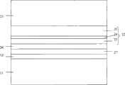
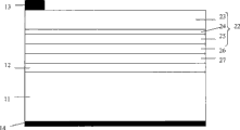
图5为半导体发光装置结构100的剖面图,其制作程序如图1至图5所示。图1所示以一发光二极管为例,包含一成长基板21,其材料可为砷化镓、硅、碳化硅、蓝宝石、磷化铟、磷化镓、氮化铝或氮化镓等。接着,在成长基板21上形成外延结构22。外延结构22通过一外延工艺所形成,例如有机金属气相沉积外延法(MOCVD)、液相外延法(LPE)或分子束外延法(MBE)等外延工艺。此外延结构22至少包含一第一电性半导体层23,例如为一n型磷化铝镓铟(AlxGa1-x)yIn1-yP层或一n型氮化铝镓铟(AlxGa1-x)yIn1-yN层;一有源层24,例如为磷化铝镓铟(AlxGa1-x)yIn1-yP或氮化铝镓铟(AlxGa1-x)yIn1-yN所形成的多重量子阱结构;以及一第二电性半导体层25,例如为一p型磷化铝镓铟(AlxGa1-x)yIn1-yP层或一p型氮化铝镓铟(AlxGa1-x)yIn1-yN层。另外,本实施例的有源层24可由例如同质结构、单异质结构、双异质结构、或是多重量子阱结构所堆叠而成。FIG. 5 is a cross-sectional view of a semiconductor light
接着,在外延结构22上形成一第二电性接触层26及一反射层27。第二电性接触层26的材料可为氧化铟锡(Indium Tin Oxide)、氧化铟(IndiumOxide)、氧化锡(Tin Oxide)、氧化镉锡(Cadmium Tin Oxide)、氧化锌(ZincOxide)、氧化镁(Magnesium Oxide)或氮化钛(Titanium Nitride)等导电氧化物材料。反射层27可为金属材料,例如铝、金、铂、锌、银、镍、锗、铟、锡等金属或其合金;也可由金属和氧化物组合而成,例如氧化铟锡/银(ITO/Ag)、氧化铟锡/氧化铝/银(ITO/AlOx/Ag)、氧化铟锡/氧化钛/氧化硅(ITO/TiOx/SiOx)、氧化钛/氧化硅/铝(TiOx/SiOx/Al)、氧化铟锡/氮化硅/铝(ITO/SiNx/Al)、氧化铟锡/氮化硅/银(ITO/SiNx/Ag)、氧化铟锡/氮化硅/氧化铝/铝(ITO/SiNx/Al2O3/Al)、或氧化铟锡/氮化硅/氧化铝/银(ITO/SiNx/Al2O3/Ag)等。Next, a second
如图2所示,包含一导电基板11,其上具有一接合层12。As shown in FIG. 2 , it includes a
接着,如图1所示将具有反射层27的外延结构22接合于如图2所示的接合层12之上,并移除成长基板21(图未示),如图3所示。接合层12的材料可为金属,例如锡化金(AuSn)、银化铟(InAg)、金化铟(InAu)、铟(In)、金(Au)、铝(Al)与银(Ag)等或上述金属的合金。Next, as shown in FIG. 1 , the
分别在第一电性半导体层23之上及导电基板11背面形成电极13、14(如图4所示)。再于第一电性半导体层23的上电极以外的区域涂布一层厚度至少为0.3mm的透明胶材15,此透明胶材可为环氧树脂(Epoxy),且透明胶材涂布面积不大于外延结构面积。再于透明胶材侧边形成一反射壁17。将波长转换结构16覆盖整个透明胶材的上表面,其中波长转换结构16至少由一种波长转换材料所构成。即形成一半导体发光装置结构100(如图5所示)。
当外延结构22被注入电流后,可激发出一原色光,此原色光经过透明胶材15后,因透明胶材穿透率接近99-100%,且侧向发光会被侧边的反射壁17把光反射回来,所以光取出效率不会降低。此原色光再进入波长转换结构16,会被波长转换结构内的波长转换材料吸收,产生一波长与原色光波长相异的变色光。因波长转换材料不限于一种,因此变色光可能含有多种颜色。When the
在本实施例中,波长转换材料为荧光粉,例如Y3Al5O12。除此之外,波长转换材料亦包含但不限于Gd3Ga5O12:Ce、(Lu,Y)3Al5O12:Ce、SrS:Eu、SrGa2S4:Eu、(Sr,Ca,Ba)(Al,Ga)2S4:Eu、(Ca,Sr)S:Eu,Mn、(Ca,Sr)S:Ce、(Sr,Ba,Ca)2Si5N8:Eu、(Ba,Sr,Ca)2SiO4:Eu、(Ca,Sr,Ba)Si2O2N2:Eu;优选地为非电绝缘性材料,如CdZnSe。In this embodiment, the wavelength conversion material is fluorescent powder, such as Y 3 Al 5 O 12 . In addition, wavelength conversion materials also include but are not limited to Gd 3 Ga 5 O 12 : Ce, (Lu, Y) 3 Al 5 O 12 : Ce, SrS: Eu, SrGa 2 S 4 : Eu, (Sr, Ca , Ba) (Al, Ga) 2 S 4 : Eu, (Ca, Sr) S: Eu, Mn, (Ca, Sr) S: Ce, (Sr, Ba, Ca) 2 Si 5 N 8 : Eu, ( Ba, Sr, Ca)2SiO 4 :Eu, (Ca,Sr,Ba)Si 2 O 2 N 2 :Eu; preferably a non-electrically insulating material such as CdZnSe.
图6为另一实施例半导体发光装置结构200的剖面图。其前段制作程序与前一实施例相同,如图1至图4所示。接着在第一电性半导体层23的上电极以外的区域涂布一层厚度至少为0.3mm的透明胶材15,此透明胶材可为环氧树脂(Epoxy),且透明胶材涂布面积不大于外延结构面积。再于透明胶材侧边形成一反射壁17,将至少一种波长转换材料均匀分布于透明胶材内,即形成一半导体发光装置结构200,如图6所示。当外延结构22被注入电流后,可激发出一原色光,此原色光经过具有波长转换材料均匀分布的透明胶材后,该原色光被波长转换材料吸收,产生一波长与原色光波长相异的变色光。因波长转换材料不限于一种,因此变色光可能含有多种颜色。FIG. 6 is a cross-sectional view of another embodiment of a semiconductor light emitting device structure 200 . Its pre-production procedure is the same as that of the previous embodiment, as shown in Figures 1 to 4. Then, a layer of transparent
图7为再一实施例半导体发光装置结构300的剖面图。其前段制作程序与前一实施例相同,如图1至图4所示。接着在第一电性半导体层23的上电极以外的区域涂布一层厚度至少为0.3mm的透明胶材15,此透明胶材15可为环氧树脂(Epoxy),且透明胶材15涂布面积不大于外延结构面积。再于透明胶材15侧边形成一反射壁17,另形成一层波长转换结构16于透明胶材15中,其中波长转换结构16至少包含一种波长转换材料,即形成一半导体发光装置结构300,如图7所示。当外延结构22被注入电流后,可激发出一原色光,此原色光经过透明胶材15后,因透明胶材15穿透率接近99-100%,且侧向发光会被侧边的反射壁17把光反射回来,所以光取出效率不会降低。此原色光再进入波长转换结构16,会被波长转换材料吸收,产生一波长与原色光波长相异的变色光。因波长转换材料不限于一种,因此变色光可能含有多种颜色。最后经过上方的透明胶材而出光。FIG. 7 is a cross-sectional view of a semiconductor light emitting
图8A为半导体发光装置结构400的俯视图,图8B为依沿a’a’虚线切开,由箭号a方向看去所得的结构剖面图,图8C为沿b’b’虚线切开,由依箭号b方向看去所得的结构剖面图。其前段制作程序与前一实施例相同,如图1至图3所示。当移除成长基板21后(图未示),在外延结构22侧面自第一电性半导体层23、有源层24、第二电性半导体层25、第二电性接触层26、反射层27、至接合层12依序由上至下蚀刻至导电基板11上表面后,再分别于第一电性半导体层23之上及导电基板11背面形成电极13、14。接下来,在第一电性半导体层23的上电极以外的区域涂布一层厚度至少为0.3mm的透明胶材15,此透明胶材可为环氧树脂(Epoxy),且透明胶材涂布面积不大于外延结构面积。将波长转换结构16覆盖整个透明胶材的上表面,其中波长转换结构16至少由一种波长转换材料所构成。为避免发光二极管侧向发光逸失,还在透明胶材15侧边及自第一电性半导体层23、有源层24、第二电性半导体层25、第二电性接触层26、反射层27、至接合层12等以上各层侧边形成一反射壁17,即形成一半导体发光装置结构400,如图8C所示。当外延结构22被注入电流后,可激发出一原色光,此原色光经过透明胶材15后,因透明胶材穿透率接近99-100%,且侧向发光会被侧边反射壁17把光反射回来,所以光取出效率不会降低。此原色光再进入波长转换结构16,会被波长转换材料吸收,产生一波长与原色光波长相异的变色光。因波长转换材料不限于一种,因此变色光可能含有多种颜色。Figure 8A is a top view of a semiconductor light emitting
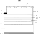
相同设计概念也可以应用于半导体发光装置封装结构1,如图9所示。一半导体发光装置500固定于一支架31上,通过电性连结将此发光装置电性连结于支架上的电路。支架之上有一碗杯32,碗杯内侧有一反射壁33,且反射壁部分区域与支架间夹角约45度。充填一透明胶材15于碗杯内,且透明胶材高度至少大于半导体发光装置500的高度,此透明胶材可为环氧树脂(Epoxy);且透明胶材涂布面积不大于外延结构面积。再形成一波长转换结构16于透明胶材之上,即形成半导体发光装置封装结构1。半导体发光装置500所产生的原色光经过透明胶材15后,因透明胶材穿透率接近99-100%,且侧向发光会被反射壁33把光反射回来,所以光取出效率不会降低。此原色光再进入波长转换结构16,会被波长转换结构内的波长转换材料吸收,产生一波长与原色光波长相异的变色光。因波长转换材料不限于一种,因此变色光可能含有多种颜色。The same design concept can also be applied to the
图10为半导体发光装置封装结构2的剖面图。其大部分制作程序与半导体发光装置封装结构1相似,但还包含一波长选择薄膜(wavelengthselection film,WSF)18形成于透明胶材15与波长转换结构16之间,其功能为使可见光通过往波长转换结构方向前进,但被波长转换结构反射回的可见光则无法通过此薄膜。FIG. 10 is a cross-sectional view of the
碗杯内侧的反射壁33设计可以如图11所示,其反射效果比图10更佳。The design of the
惟上述实施例仅为例示性说明本发明的原理及其功效,而非用于限制本发明。任何本领域的技术人员均可在不违背本发明的技术原理及精神的情况下,对上述实施例进行修改及变化。因此本发明的权利保护范围如后述的权利要求所列。However, the above-mentioned embodiments are only for illustrating the principles and effects of the present invention, rather than limiting the present invention. Any person skilled in the art can modify and change the above-mentioned embodiments without violating the technical principle and spirit of the present invention. Therefore, the protection scope of the present invention is as listed in the following claims.
Claims (10)
Priority Applications (3)
| Application Number | Priority Date | Filing Date | Title |
|---|---|---|---|
| CN201610167887.2A CN105609619B (en) | 2008-09-12 | 2008-09-12 | Semiconductor light-emitting device and its packaging structure |
| CN2008101494130A CN101673787B (en) | 2008-09-12 | 2008-09-12 | Semiconductor light emitting device and packaging structure thereof |
| CN201210401928.1A CN102903832B (en) | 2008-09-12 | 2008-09-12 | Semiconductor light emitting device and packaging structure thereof |
Applications Claiming Priority (1)
| Application Number | Priority Date | Filing Date | Title |
|---|---|---|---|
| CN2008101494130A CN101673787B (en) | 2008-09-12 | 2008-09-12 | Semiconductor light emitting device and packaging structure thereof |
Related Child Applications (2)
| Application Number | Title | Priority Date | Filing Date |
|---|---|---|---|
| CN201610167887.2A Division CN105609619B (en) | 2008-09-12 | 2008-09-12 | Semiconductor light-emitting device and its packaging structure |
| CN201210401928.1A Division CN102903832B (en) | 2008-09-12 | 2008-09-12 | Semiconductor light emitting device and packaging structure thereof |
Publications (2)
| Publication Number | Publication Date |
|---|---|
| CN101673787A CN101673787A (en) | 2010-03-17 |
| CN101673787B true CN101673787B (en) | 2012-12-12 |
Family
ID=42020884
Family Applications (2)
| Application Number | Title | Priority Date | Filing Date |
|---|---|---|---|
| CN2008101494130A Active CN101673787B (en) | 2008-09-12 | 2008-09-12 | Semiconductor light emitting device and packaging structure thereof |
| CN201610167887.2A Active CN105609619B (en) | 2008-09-12 | 2008-09-12 | Semiconductor light-emitting device and its packaging structure |
Family Applications After (1)
| Application Number | Title | Priority Date | Filing Date |
|---|---|---|---|
| CN201610167887.2A Active CN105609619B (en) | 2008-09-12 | 2008-09-12 | Semiconductor light-emitting device and its packaging structure |
Country Status (1)
| Country | Link |
|---|---|
| CN (2) | CN101673787B (en) |
Families Citing this family (4)
| Publication number | Priority date | Publication date | Assignee | Title |
|---|---|---|---|---|
| TW201208143A (en) * | 2010-08-06 | 2012-02-16 | Semileds Optoelectronics Co | White LED device and manufacturing method thereof |
| CN102593310A (en) * | 2011-01-11 | 2012-07-18 | 旭明光电股份有限公司 | Wafer type light-emitting device with precisely coated wavelength conversion layer |
| WO2013144834A1 (en) | 2012-03-30 | 2013-10-03 | Koninklijke Philips N.V. | Light emitting device with wavelength converting side coat |
| WO2014062871A1 (en) * | 2012-10-19 | 2014-04-24 | Osram Sylvania Inc. | Index matched composite materials and light sources incorporating the same |
Citations (4)
| Publication number | Priority date | Publication date | Assignee | Title |
|---|---|---|---|---|
| CN1218996A (en) * | 1997-11-27 | 1999-06-09 | 陈兴 | Multiple colour light emitting diode body |
| CN1734798A (en) * | 2004-08-02 | 2006-02-15 | 晶元光电股份有限公司 | Omni-directional reflector LED with transparent conductive layer |
| CN1742382A (en) * | 2003-01-27 | 2006-03-01 | 3M创新有限公司 | Phosphor-based light source with reflective polarizer |
| CN1805158A (en) * | 2005-01-14 | 2006-07-19 | 财团法人工业技术研究院 | A light-emitting diode with a quasi-omnidirectional reflector |
Family Cites Families (3)
| Publication number | Priority date | Publication date | Assignee | Title |
|---|---|---|---|---|
| US7521727B2 (en) * | 2006-04-26 | 2009-04-21 | Rohm And Haas Company | Light emitting device having improved light extraction efficiency and method of making same |
| WO2008056296A1 (en) * | 2006-11-06 | 2008-05-15 | Koninklijke Philips Electronics N.V. | Wavelength converting elements with reflective edges |
| CN201069780Y (en) * | 2007-07-18 | 2008-06-04 | 宁波安迪光电科技有限公司 | High power white light LED and its chip |
-
2008
- 2008-09-12 CN CN2008101494130A patent/CN101673787B/en active Active
- 2008-09-12 CN CN201610167887.2A patent/CN105609619B/en active Active
Patent Citations (4)
| Publication number | Priority date | Publication date | Assignee | Title |
|---|---|---|---|---|
| CN1218996A (en) * | 1997-11-27 | 1999-06-09 | 陈兴 | Multiple colour light emitting diode body |
| CN1742382A (en) * | 2003-01-27 | 2006-03-01 | 3M创新有限公司 | Phosphor-based light source with reflective polarizer |
| CN1734798A (en) * | 2004-08-02 | 2006-02-15 | 晶元光电股份有限公司 | Omni-directional reflector LED with transparent conductive layer |
| CN1805158A (en) * | 2005-01-14 | 2006-07-19 | 财团法人工业技术研究院 | A light-emitting diode with a quasi-omnidirectional reflector |
Non-Patent Citations (1)
| Title |
|---|
| JP特开2007-43074A 2007.02.15 |
Also Published As
| Publication number | Publication date |
|---|---|
| CN101673787A (en) | 2010-03-17 |
| CN105609619B (en) | 2019-07-19 |
| CN105609619A (en) | 2016-05-25 |
Similar Documents
| Publication | Publication Date | Title |
|---|---|---|
| TWI478370B (en) | Semiconductor light emitting device with wavelength conversion structure and package structure thereof | |
| TWI404228B (en) | Semiconductor light emitting device and method of manufacturing same | |
| JP5973693B2 (en) | Light emitting device and light emitting device package | |
| US9136447B2 (en) | Light emitting device and method of manufacturing the same | |
| US8698176B2 (en) | Light emitting device and lighting system | |
| US11545595B2 (en) | Contact structures for light emitting diode chips | |
| JP6542509B2 (en) | Phosphor and light emitting device package including the same | |
| WO2007102534A1 (en) | Chip type semiconductor light emitting element | |
| TW201637247A (en) | Method for producing light-emitting element transfer sheet, method for manufacturing light-emitting device, light-emitting element transfer sheet, and light-emitting device | |
| US8729568B2 (en) | Light emitting device | |
| JP4773755B2 (en) | Chip-type semiconductor light emitting device | |
| CN107112404A (en) | Light-emitting device | |
| JP2016082229A (en) | Light emitting device, light emitting device package, and lighting device including package | |
| CN101673787B (en) | Semiconductor light emitting device and packaging structure thereof | |
| US10199540B2 (en) | Light emitting diode, light emitting diode package including same, and lighting system including same | |
| CN102800800A (en) | Light-emitting diode device and production method thereof | |
| JP2013012709A (en) | Nitride-based light-emitting diode element and light-emitting method | |
| CN102903832B (en) | Semiconductor light emitting device and packaging structure thereof | |
| CN101488541A (en) | Semiconductor light emitting device and method for manufacturing the same | |
| KR102261954B1 (en) | Phosphor film, light emitting device package and lighting apparatus including the same | |
| KR102507444B1 (en) | Light emitting device and display device including the same | |
| KR102131309B1 (en) | Phosphor and light emitting device package including the same | |
| KR102075132B1 (en) | Light emitting device | |
| KR101722623B1 (en) | Light-emitting element and Light-emitting element package | |
| KR20120045119A (en) | A light emitting device and a light emitting device package |
Legal Events
| Date | Code | Title | Description |
|---|---|---|---|
| C06 | Publication | ||
| PB01 | Publication | ||
| C10 | Entry into substantive examination | ||
| SE01 | Entry into force of request for substantive examination | ||
| C14 | Grant of patent or utility model | ||
| GR01 | Patent grant |