CN101673717A - Semiconductor device and method of manufacturing thereof - Google Patents
Semiconductor device and method of manufacturing thereof Download PDFInfo
- Publication number
- CN101673717A CN101673717A CN200910179066A CN200910179066A CN101673717A CN 101673717 A CN101673717 A CN 101673717A CN 200910179066 A CN200910179066 A CN 200910179066A CN 200910179066 A CN200910179066 A CN 200910179066A CN 101673717 A CN101673717 A CN 101673717A
- Authority
- CN
- China
- Prior art keywords
- wiring
- resin layer
- semiconductor device
- addition
- external terminals
- Prior art date
- Legal status (The legal status is an assumption and is not a legal conclusion. Google has not performed a legal analysis and makes no representation as to the accuracy of the status listed.)
- Granted
Links
Images


Classifications
-
- H10W72/00—
-
- H10W74/129—
-
- H10W72/071—
-
- H10W74/00—
Landscapes
- Internal Circuitry In Semiconductor Integrated Circuit Devices (AREA)
- Structures Or Materials For Encapsulating Or Coating Semiconductor Devices Or Solid State Devices (AREA)
- Dicing (AREA)
- Encapsulation Of And Coatings For Semiconductor Or Solid State Devices (AREA)
Abstract
一种半导体装置(1),在具备多个电极(9)的半导体元件(2)上,形成有多个树脂层、与电极(9)进行电连接的多个配线(4)、以及电连接到该配线(4)的多个外部端子(7),其特征是,在多个配线(4)中,其一部分的第一配线(4a)形成于一个树脂层(第一树脂层3)或者叠层了的多个树脂层的底面,且在多个配线(4)中,除该一部分之外的第二配线(4b)形成于一个树脂层(第一树脂层3)或者叠层了的多个树脂层的表面。由此,本发明提供一种能够高密度地形成配线以及外部端子的半导体装置及其制造方法、搭载该半导体装置的电路基板以及具备该半导体装置的电子设备。
A semiconductor device (1), in which a plurality of resin layers, a plurality of wirings (4) electrically connected to the electrodes (9), and an electrical The plurality of external terminals (7) connected to the wiring (4) is characterized in that, among the plurality of wirings (4), a part of the first wiring (4a) is formed on one resin layer (first resin layer 3) or the bottom surface of a plurality of laminated resin layers, and among the plurality of wirings (4), the second wiring (4b) except for this part is formed in one resin layer (the first resin layer 3 ) or the surface of multiple laminated resin layers. Accordingly, the present invention provides a semiconductor device capable of forming wiring and external terminals at a high density, a manufacturing method thereof, a circuit board on which the semiconductor device is mounted, and electronic equipment including the semiconductor device.
Description
本申请是基于申请号为200410104968.5、发明名称为“半导体装置及其制造方法、电路基板以及电子设备”、申请日为2004年12月15日的专利申请的分案申请。This application is a divisional application based on the patent application with the application number 200410104968.5, the title of the invention is "semiconductor device and its manufacturing method, circuit substrate and electronic equipment", and the filing date is December 15, 2004.
技术领域 technical field
本发明涉及半导体装置及其制造方法、电路基板以及电子设备,尤其涉及能形成多个外部端子的半导体装置及其制造方法、搭载该半导体装置的电路基板以及具备该半导体装置的电子设备。The present invention relates to a semiconductor device and its manufacturing method, a circuit board, and electronic equipment, and more particularly, to a semiconductor device capable of forming a plurality of external terminals, its manufacturing method, a circuit board on which the semiconductor device is mounted, and electronic equipment including the semiconductor device.
背景技术 Background technique
要以高密度安装半导体装置,最好不对半导体芯片进行封装而以原状态进行裸片式安装。但是,在裸片式安装中,由于对半导体芯片的保护不充分,因此很难对其进行操作。所以,人们提出了使用CSP(Chip SizePackage)的半导体装置,特别是近年来,开发出了从晶片划片(切断)后直接以该状态作为半导体装置的晶片级CSP。在该晶片级CSP中,在形成有微小的晶体管等的硅晶片的表面形成树脂层或者配线,并通过切断成一个一个的半导体装置,从而制造半导体装置。In order to mount semiconductor devices at a high density, it is preferable to perform bare-die mounting without packaging the semiconductor chips. However, in bare die mounting, since the protection of the semiconductor chip is not sufficient, it is difficult to handle it. Therefore, semiconductor devices using CSP (Chip Size Package) have been proposed, and especially in recent years, wafer-level CSPs have been developed that use the state as a semiconductor device directly after dicing (cutting) from a wafer. In this wafer-level CSP, a resin layer or wiring is formed on the surface of a silicon wafer on which minute transistors and the like are formed, and the semiconductor devices are cut into individual semiconductor devices to manufacture semiconductor devices.
以往的适用晶片级CSP的半导体装置的制造方法中,在硅晶片的表面形成树脂层时,不在划片的部分形成树脂层,从而防止半导体装置端部出现缺口以及树脂层剥落(例如,参照专利文献1)。In the manufacturing method of the semiconductor device that is applicable to wafer-level CSP in the past in the past, when forming resin layer on the surface of silicon wafer, do not form resin layer in the part of dicing, thereby prevent the notch and resin layer from peeling off at the end of semiconductor device (for example, refer to patent Literature 1).
[专利文献]国际公开第01/071805号单行本(图1、图14)[Patent Document] International Publication No. 01/071805 pamphlet (Fig. 1, Fig. 14)
但是,以往的适用晶片级CSP的半导体装置的制造方法中(例如,参照专利文献1),在半导体元件的中心附近形成有树脂层和外部端子,且从形成于半导体元件的外周部的电极延伸电极而连接到该外部端子。此时,由于仅在树脂层的表面形成配线,因此能够形成配线以及外部端子的部分的面积很小,很难形成多个外部端子,且很难实现配线以及外部端子的高密度化,而这些成为了问题点。However, in a conventional semiconductor device manufacturing method to which wafer-level CSP is applied (for example, refer to Patent Document 1), a resin layer and external terminals are formed near the center of the semiconductor element and extend from electrodes formed on the outer periphery of the semiconductor element. The electrode is connected to the external terminal. At this time, since wiring is formed only on the surface of the resin layer, the area where wiring and external terminals can be formed is small, and it is difficult to form a large number of external terminals, and it is difficult to increase the density of wiring and external terminals. , and these become problematic points.
发明内容 Contents of the invention
本发明鉴于以上的事实,其目的在于提供一种能够高密度地形成配线以及外部端子的半导体装置及其制造方法,搭载该半导体装置的电路基板以及具备该半导体装置的电子设备。In view of the above facts, an object of the present invention is to provide a semiconductor device capable of forming wiring and external terminals at a high density, a method for manufacturing the same, a circuit board on which the semiconductor device is mounted, and electronic equipment including the semiconductor device.
本发明的半导体装置,在具备多个电极的半导体元件上,形成有树脂层、与所述电极电连接的配线、以及与该配线电连接的多个外部端子,其特征是:在多个所述配线中,第一配线形成于所述树脂层或者叠层了的多个树脂层的第一表面;所述多个配线中的第二配线形成于所述树脂层或者叠层了的多个树脂层的与所述第一表面相反侧的面即第二表面;所述第一配线与第二配线立体交叉。In the semiconductor device of the present invention, a resin layer, wiring electrically connected to the electrodes, and a plurality of external terminals electrically connected to the wiring are formed on a semiconductor element having a plurality of electrodes, and is characterized in that: Among the wirings, the first wiring is formed on the first surface of the resin layer or a plurality of laminated resin layers; the second wiring among the plurality of wirings is formed on the resin layer or The second surface is a surface opposite to the first surface of the laminated plurality of resin layers; the first wiring and the second wiring are three-dimensionally intersected.
本发明的半导体装置,在具备多个电极的半导体元件上,形成有多个树脂层、与电极进行电连接的多个配线、以及电连接到该配线的多个外部端子,其特征是:在多个配线中,其一部分的第一配线形成于一个树脂层或者叠层了的多个树脂层的底面;且在多个配线中,除该一部分之外的第二配线形成于一个树脂层或者叠层了的多个树脂层的表面;所述第一配线与第二配线以立体交叉的方式形成。In the semiconductor device of the present invention, a plurality of resin layers, a plurality of wirings electrically connected to the electrodes, and a plurality of external terminals electrically connected to the wirings are formed on a semiconductor element having a plurality of electrodes, and is characterized in that : Among the plurality of wirings, a part of the first wiring is formed on the bottom surface of one resin layer or a plurality of laminated resin layers; and among the plurality of wirings, the second wiring other than the part Formed on the surface of one resin layer or a plurality of laminated resin layers; the first wiring and the second wiring are formed in a three-dimensional crossing manner.
在多个配线中,其一部分的第一配线形成于一个树脂层或者叠层了的多个树脂层的底面,且除了这一部分的第二配线形成于一个树脂层或者叠层了的多个树脂层的表面,因此,扩宽了能够形成配线的面积,从而可以形成多个配线以及外部端子。另外,由于能够以立体式交叉形状形成,因此能够以高密度形成外部端子。Among the plurality of wirings, a part of the first wiring is formed on the bottom surface of one resin layer or a plurality of laminated resin layers, and other than this part of the second wiring is formed on a resin layer or a laminated resin layer. The surface of the plurality of resin layers, therefore, widens the area where wiring can be formed, so that a plurality of wiring and external terminals can be formed. In addition, since it can be formed in a three-dimensional cross shape, external terminals can be formed at high density.
另外关于本发明的半导体装置,在所述的多个电极之中,在未与第一配线连接的电极的表面上,形成有与第一配线相同材料的金属膜。Further, in the semiconductor device of the present invention, among the plurality of electrodes, a metal film of the same material as that of the first wiring is formed on the surface of an electrode not connected to the first wiring.
通过在未与第一配线连接的电极的表面上,形成有与第一配线相同材料的金属膜,可以防止这些电极的氧化和腐蚀。By forming the metal film of the same material as that of the first wiring on the surfaces of the electrodes not connected to the first wiring, oxidation and corrosion of these electrodes can be prevented.
另外关于本发明的半导体装置,所述的第一配线,连接到多个外部端子中的至少位于半导体元件的最外周部侧的外部端子。In addition, in the semiconductor device of the present invention, the first wiring is connected to at least an external terminal located on the outermost peripheral side of the semiconductor element among the plurality of external terminals.
半导体元件的外周部附近,由热应力等而受到很大的应力。因此,通过使比较难断线的第一配线连接到多个外部端子中的至少位于半导体元件的最外周部侧的外部端子,可以防止断线。The vicinity of the outer periphery of the semiconductor element receives a large stress due to thermal stress or the like. Therefore, disconnection can be prevented by connecting the relatively difficult-to-disconnect first wiring to at least the external terminal located on the outermost peripheral portion side of the semiconductor element among the plurality of external terminals.
另外关于本发明的半导体装置,所述的半导体装置采用的封装方式是芯片尺寸封装方式。In addition, with regard to the semiconductor device of the present invention, the packaging method adopted by the semiconductor device is a chip size packaging method.
在所述的半导体装置采用芯片尺寸封装方式(CSP)的情况下,形成所述结构的配线,则可以实现配线以及外部端子的高密度化。When the above-mentioned semiconductor device adopts a chip size package (CSP), forming the wiring of the above-mentioned structure can realize high density of wiring and external terminals.
另外关于本发明的半导体装置,所述外部端子是由软钎球构成。In addition, in the semiconductor device of the present invention, the external terminals are formed of solder balls.
芯片尺寸封装的半导体装置,作为外部端子多使用软钎球。根据所述的结构的配线,可以高密度地形成由该软钎球构成的外部端子。Semiconductor devices in chip size packages often use solder balls as external terminals. According to the wiring of the above-described structure, the external terminals composed of the solder balls can be formed at a high density.
另外关于本发明的半导体装置,在所述的一个树脂层或者叠层了的多个树脂层中形成有通孔。In addition, in the semiconductor device of the present invention, through holes are formed in the above-mentioned one resin layer or the plurality of laminated resin layers.
由于在所述的一个树脂层或者叠层了的多个树脂层中形成有通孔,因此可以很容易地将在一个树脂层或者叠层了的多个树脂层的底面形成的第一配线连接到外部端子,从而提高了连接可靠性。Since a through hole is formed in the one resin layer or a plurality of laminated resin layers, the first wiring formed on the bottom surface of one resin layer or a plurality of laminated resin layers can be easily connected. Connect to external terminals, thus improving connection reliability.
另外关于本发明的半导体装置,通过对由硅晶片构成的半导体元件的集合体经划片而进行切断,制造该半导体装置。In addition, the semiconductor device of the present invention is manufactured by dicing and cutting an assembly of semiconductor elements composed of a silicon wafer.
例如,通过对形成有微小晶体管等的硅晶片经划片而进行切断,从而制造了半导体装置,因此可以由一片硅晶片获得多个半导体装置。For example, since a semiconductor device is manufactured by dicing and cutting a silicon wafer on which minute transistors and the like are formed, a plurality of semiconductor devices can be obtained from one silicon wafer.
另外关于本发明的半导体装置,在所述的多个树脂层中,至少一个树脂层以避开半导体元件的集合体的经划片而切断的部分的方式形成。In addition, in the semiconductor device of the present invention, among the plurality of resin layers, at least one resin layer is formed so as to avoid a portion of the assembly of semiconductor elements cut by dicing.
由于至少一个树脂层以避开半导体元件的集合体的经划片而切断的部分的方式形成,因此可以防止半导体装置的端部产生缺口以及树脂层剥落。Since at least one resin layer is formed so as to avoid the dicing-cut portion of the assembly of semiconductor elements, it is possible to prevent chipping at the end of the semiconductor device and peeling of the resin layer.
另外关于本发明的半导体装置,至少一个树脂层在形成有电极的部分形成。In addition, in the semiconductor device of the present invention, at least one resin layer is formed in the portion where the electrode is formed.
例如,如果所述的一个树脂层或者叠层了的多个树脂层,在形成有电极的部分形成,则形成外部端子的区域就会扩宽,从而可以形成多个外部端子。For example, if one resin layer or a plurality of laminated resin layers is formed in a portion where an electrode is formed, the area where an external terminal is to be formed is widened, and a plurality of external terminals can be formed.
本发明的半导体装置的制造方法,在具备多个电极的半导体元件上,形成与电极进行电连接的多个配线、和电连接到该配线的多个外部端子,其特征是:在多个配线中,形成其一部分的第一配线之后,在该第一配线的表面形成至少一个树脂层或者叠层了的多个树脂层,且在多个配线中,将除该一部分之外的第二配线形成于一个树脂层或者叠层了的多个树脂层的表面,并且将所述第一配线与第二配线以立体交叉的方式形成。In the method of manufacturing a semiconductor device of the present invention, on a semiconductor element having a plurality of electrodes, a plurality of wirings electrically connected to the electrodes and a plurality of external terminals electrically connected to the wirings are formed, and it is characterized in that: Among the wirings, after the first wiring which is a part thereof is formed, at least one resin layer or a plurality of laminated resin layers is formed on the surface of the first wiring, and among the plurality of wirings, the part will be removed The other second wiring is formed on the surface of one resin layer or a plurality of laminated resin layers, and the first wiring and the second wiring are formed in a three-dimensional crossing manner.
关于如上的本发明制造方法,在多个配线中,形成其一部分的第一配线之后,在该第一配线的表面形成至少一个树脂层或者叠层了的多个树脂层,且在多个配线中,将除该一部分之外的第二配线形成于一个树脂层或者叠层了的多个树脂层的表面,因此,能够形成配线的部分的面积扩大到树脂层的两面,从而可以形成多个配线以及外部端子。另外,由于能够以立体式交叉形状形成,因此能够以高密度形成外部端子。With regard to the manufacturing method of the present invention as described above, after forming a part of the first wiring among the plurality of wirings, at least one resin layer or a plurality of laminated resin layers is formed on the surface of the first wiring, and Among the plurality of wirings, the second wiring other than this part is formed on the surface of one resin layer or a plurality of laminated resin layers, so the area of the part where the wiring can be formed is expanded to both sides of the resin layer. , so that a plurality of wiring and external terminals can be formed. In addition, since it can be formed in a three-dimensional cross shape, external terminals can be formed at high density.
另外关于本发明的半导体装置的制造方法,在所述的多个电极之中,在未与第一配线连接的电极的表面上,形成与第一配线相同材料的金属膜。In addition, in the method of manufacturing a semiconductor device according to the present invention, among the plurality of electrodes, a metal film of the same material as that of the first wiring is formed on the surface of an electrode not connected to the first wiring.
通过在未与第一配线连接的电极的表面上,形成与第一配线相同材料的金属膜,可以防止这些电极的氧化和腐蚀。By forming a metal film of the same material as that of the first wiring on the surfaces of the electrodes not connected to the first wiring, oxidation and corrosion of these electrodes can be prevented.
另外关于本发明的半导体装置的制造方法,将所述的第一配线连接到多个外部端子中的至少位于半导体元件的最外周部侧的外部端子。In addition, in the method of manufacturing a semiconductor device according to the present invention, the first wiring is connected to at least an external terminal located on the outermost peripheral side of the semiconductor element among the plurality of external terminals.
半导体元件的外周部附近由热应力等而会受到很大的应力。因此,通过将比较难断线的第一配线连接到多个外部端子中的至少位于半导体元件的最外周部侧的外部端子,可以防止断线。The vicinity of the outer periphery of the semiconductor element receives a large stress due to thermal stress or the like. Therefore, disconnection can be prevented by connecting the relatively difficult-to-break first wiring to at least the external terminal located on the outermost peripheral portion side of the semiconductor element among the plurality of external terminals.
另外关于本发明的半导体装置的制造方法,所述的半导体装置采用芯片尺寸封装方式进行封装。In addition, with regard to the manufacturing method of the semiconductor device of the present invention, the semiconductor device is packaged in a chip size packaging manner.
在所述的半导体装置采用芯片尺寸封装方式(CSP)的情况下,形成所述结构的配线,则可以实现配线以及外部端子的高密度化。When the above-mentioned semiconductor device adopts a chip size package (CSP), forming the wiring of the above-mentioned structure can realize high density of wiring and external terminals.
另外关于本发明的半导体装置的制造方法,所述外部端子是由软钎球构成。In addition, in the method of manufacturing a semiconductor device according to the present invention, the external terminals are formed of solder balls.
芯片尺寸封装的半导体装置,作为外部端子多使用软钎球。通过形成具有所述的结构的配线,可以高密度地形成由该软钎球构成的外部端子。Semiconductor devices in chip size packages often use solder balls as external terminals. By forming the wiring having the above-described structure, external terminals composed of the solder balls can be formed at high density.
另外关于本发明的半导体装置的制造方法,在所述的一个树脂层或者叠层了的多个树脂层中形成通孔。In addition, in the method of manufacturing a semiconductor device according to the present invention, a via hole is formed in the above-mentioned one resin layer or a plurality of stacked resin layers.
由于在所述的一个树脂层或者叠层了的多个树脂层中形成了通孔,因此可以很容易地将在一个树脂层或者叠层了的多个树脂层的底面形成的第一配线连接到外部端子,从而提高了连接可靠性。Since the through holes are formed in the one resin layer or the laminated resin layers, the first wiring formed on the bottom surface of the one resin layer or the laminated resin layers can be easily Connect to external terminals, thus improving connection reliability.
另外关于本发明的半导体装置的制造方法,通过对由硅晶片构成的半导体元件的集合体经划片而进行切断,制造该半导体装置。In addition, in the method of manufacturing a semiconductor device of the present invention, the semiconductor device is manufactured by dicing and cutting an assembly of semiconductor elements made of a silicon wafer.
例如,通过对形成有微小晶体管等的硅晶片经划片而进行切断,从而制造了半导体装置,因此可以由一片硅晶片获得多个半导体装置。For example, since a semiconductor device is manufactured by dicing and cutting a silicon wafer on which minute transistors and the like are formed, a plurality of semiconductor devices can be obtained from one silicon wafer.
另外关于本发明的半导体装置的制造方法,在所述的多个树脂层中,至少一个树脂层以避开半导体元件的集合体的经划片而切断的部分的方式形成。In addition, in the method of manufacturing a semiconductor device according to the present invention, among the plurality of resin layers, at least one resin layer is formed so as to avoid a portion of the assembly of semiconductor elements cut by dicing.
由于至少一个树脂层以避开半导体元件的集合体的经划片而切断的部分的方式形成,因此可以防止半导体装置的端部产生缺口以及树脂层剥落。Since at least one resin layer is formed so as to avoid the dicing-cut portion of the assembly of semiconductor elements, it is possible to prevent chipping at the end of the semiconductor device and peeling of the resin layer.
另外关于本发明的半导体装置的制造方法,至少将一个树脂层在形成有电极的部分形成。In addition, in the method of manufacturing a semiconductor device of the present invention, at least one resin layer is formed in a portion where an electrode is formed.
例如,如果所述的一个树脂层或者叠层了的多个树脂层,在形成有电极的部分形成,则形成外部端子的区域就会扩宽,从而可以形成多个外部端子。For example, if one resin layer or a plurality of laminated resin layers is formed in a portion where an electrode is formed, the area where an external terminal is to be formed is widened, and a plurality of external terminals can be formed.
本发明的电路基板,其特征是搭载有所述的任何一个半导体装置。The circuit board of the present invention is characterized in that any one of the semiconductor devices described above is mounted thereon.
由于该电路基板搭载有所述的任何一个半导体装置,且在该半导体装置上以高密度形成有外部端子,因此可以实现电路基板的小型化以及高性能化。Since any one of the aforementioned semiconductor devices is mounted on the circuit board, and the external terminals are formed at a high density on the semiconductor device, the circuit board can be reduced in size and high in performance.
本发明的电子设备,其特征是搭载有所述的任何一个半导体装置。The electronic equipment of the present invention is characterized in that any one of the semiconductor devices described above is mounted.
由于该电子设备上搭载有所述的任何一个半导体装置,因此可以实现电路设备的小型化以及高性能化。Since any one of the semiconductor devices described above is mounted on the electronic device, it is possible to realize miniaturization and high performance of the circuit device.
附图说明 Description of drawings
图1是表示本发明的本实施方式1的半导体装置的俯视图以及纵截面图。1 is a plan view and a longitudinal sectional view showing a semiconductor device according to
图2是表示作为半导体元件的集合体的硅晶片的俯视图。FIG. 2 is a plan view showing a silicon wafer as an aggregate of semiconductor elements.
图3是表示本实施方式2的半导体装置的制造方法的部分俯视图以及部分纵截面图。3 is a partial plan view and a partial longitudinal sectional view showing a method of manufacturing a semiconductor device according to
图4是表示图3的制造工序的后续工序的部分俯视图以及部分纵截面图。4 is a partial plan view and a partial longitudinal sectional view showing steps subsequent to the manufacturing process shown in FIG. 3 .
图5是表示图4的制造工序的后续工序的部分俯视图以及部分纵截面图。FIG. 5 is a partial plan view and a partial longitudinal sectional view showing steps subsequent to the manufacturing process shown in FIG. 4 .
图6是表示本发明的实施方式3的电路基板的实例的立体示意图。6 is a schematic perspective view showing an example of a circuit board according to
图7是表示本发明的实施方式3的电子设备的实例的图。FIG. 7 is a diagram showing an example of an electronic device according to
图中:1-半导体装置,2-半导体元件,3-第一树脂层,4-配线,4a-第一配线,4b-第二配线,5-第二树脂层,6-第三树脂层,7-外部端子,8-钝化膜,9-电极,10-第一陆地,11-硅晶片,14-第一通孔,15-第二通孔,17-第二陆地,100-电路基板,200-笔记本型个人电脑,300-携带电话。In the figure: 1-semiconductor device, 2-semiconductor element, 3-first resin layer, 4-wiring, 4a-first wiring, 4b-second wiring, 5-second resin layer, 6-third Resin layer, 7-external terminal, 8-passivation film, 9-electrode, 10-first land, 11-silicon wafer, 14-first through hole, 15-second through hole, 17-second land, 100 -circuit board, 200-notebook personal computer, 300-mobile phone.
具体实施方式 Detailed ways
(本实施方式1)(this embodiment 1)
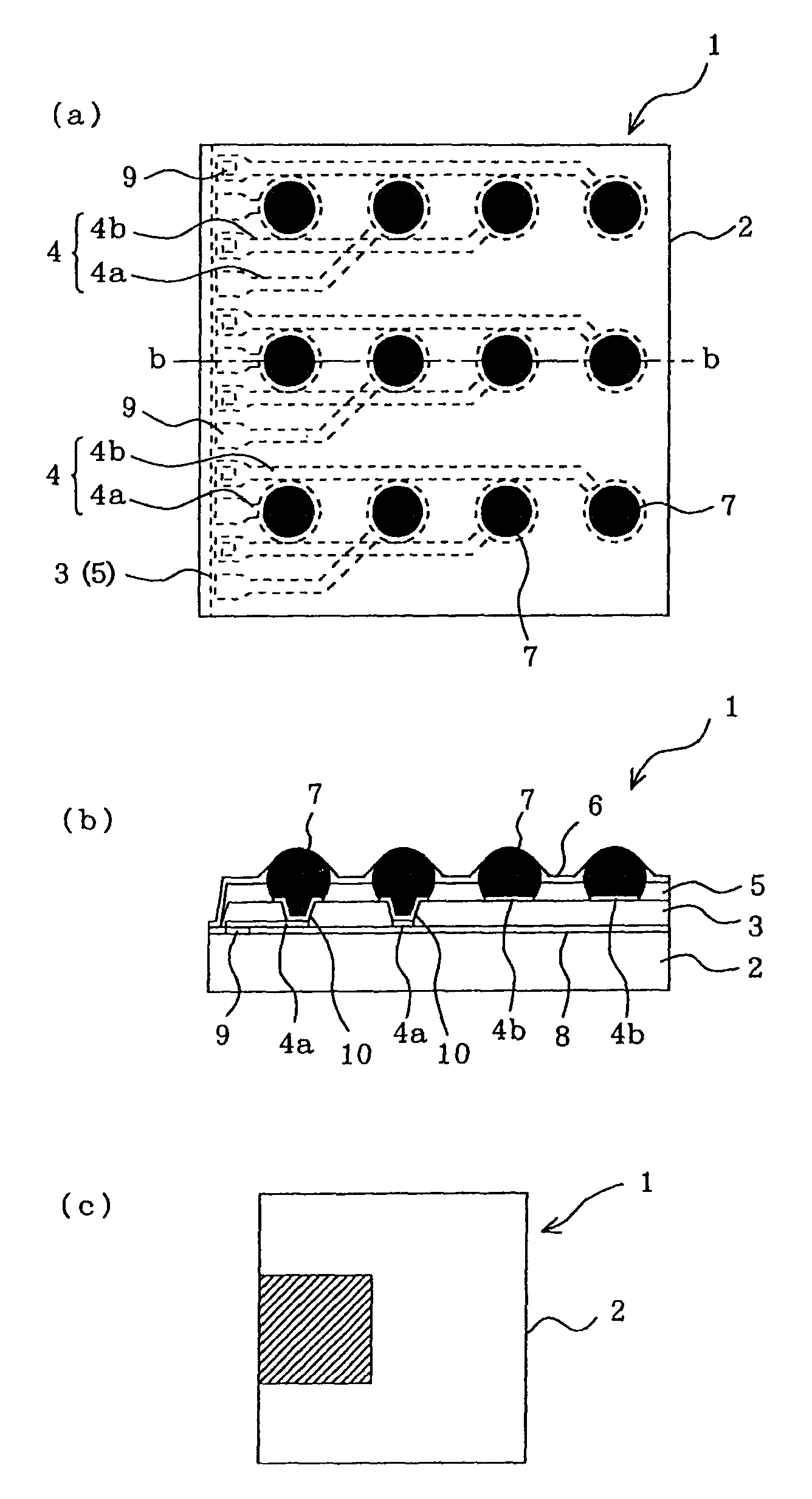
图1是表示本发明的本实施方式1的半导体装置的俯视图以及纵截面图。图1(a)和图1(b)表示了半导体装置1的侧面附近的一部分,更具体地说,是图1(c)的斜线部所示的部分。半导体装置1的其它部分是使图1(a)所示的结构大致对称地形成。另外,在图1(a)中,以一部分透明的方式显示。另外图1(b)是图1(a)的沿b-b线的纵截面图。1 is a plan view and a longitudinal sectional view showing a semiconductor device according to
本实施方式1的半导体装置1主要具有以下结构:在半导体元件2的一方的面,形成有第一树脂层3、配线4、第二树脂层5、第三树脂层6、外部端子7。
另外,在多个配线4中,其一部分构成形成于第一树脂层3的半导体元件2侧的面上的第一配线4a,且除这一部分之外的其他配线构成形成于第一树脂层3的外部端子7侧的面的第二配线4b。另外,在半导体元件2的一方的表面上形成有由绝缘体构成的钝化膜8以及电极9,且第一配线4a形成于钝化膜8的表面。In addition, among the plurality of
设置有多个电极9和配线4,且构成电连接的状态。另外,在各个配线4上设置有与配线4电连接的外部端子7,其结果电极9和外部端子7处于导通的状态。A plurality of
另外,在本实施方式1中,为了加固外部端子7的底部而设置了第三树脂层6,但也没必要一定设置。In addition, in the first embodiment, the
通过对硅晶片的前处理,半导体元件2形成了多个如微小的晶体管。而且,在硅晶片上形成第一树脂层3、外部端子7等之后,通过对硅晶片以划片的方式切断,制造一个一个的半导体装置1。由此,对硅晶片划片后即成为半导体装置的元件,就是被称为晶片级CSP的元件。该晶片级CSP是被称为CSP(chip·size·package,即,芯片尺寸封装)的封装方法的一种,它比以往的CSP实现了更加小型化。另外,在本实施方式1中,作为半导体元件2使用硅(主要是单晶),但也可以使用如镓等其他半导体材料。Through the pre-processing of the silicon wafer, the
在上述的半导体装置2的一方的面,形成有薄的钝化膜8和由铝等构成的电极9,且在钝化膜8的表面上形成有第一配线4a以及第一树脂层3。在本实施方式1中,多个电极9位于半导体元件2的外周部,且第一树脂层3还形成于电极9形成的部分之上。通过形成第一树脂层3,可扩宽形成外部端子7的区域,从而能够形成多个外部端子7。另外,第一树脂层3还形成于半导体元件2的最外侧的外周部。在这里,作为第一树脂层3的材料,可使用聚酰亚胺树脂、硅改性聚酰亚胺树脂、环氧树脂、硅改性环氧树脂、酚醛系树脂、丙烯酸树脂、苯并环丁烯(BCB、BenzoCycloButene)、聚苯并噁唑(PBO、PolyBenzOxazole)等。On one side of the above-mentioned
如上所述,配线4的一部分构成第一配线部4a,而除该部分的其他配线构成第二配线板4b。第一配线4a连接到多个电极9中的一部分,并形成于第一树脂层3的半导体元件2侧的面。另外,第二布线4b连接在未与第一布线4a连接的电极9上,形成于第一树脂层3的外部端子7侧的面上。第二配线4b经由形成于第一树脂层3的电极9的第二通孔(将在本实施方式2中详述)连接到电极9,并从第二通孔提升至第一树脂层3的外部端子7侧的面。另外,在第一配线4a的与电极9接触的部分的另一端,形成有用于连接外部端子7和第一配线4a的第一陆地(land)10(将在本实施方式2中详述)。As described above, a part of the
例如,如果将配线4全部形成于第一树脂层3的外部端子7侧的面,则能够形成配线4的部分的面积就会减少,且由于无法立体交叉配线4,因此无法高密度地形成配线4和外部端子7。因此,在本实施方式1中,通过在第一树脂层3的两面形成配线4,实现了配线4以及外部端子7的高密度化。For example, if all the
第一配线4a,例如通过叠层多个由钛·钨合金构成的层和由铜构成的层而形成。另外,第二配线4b也以与第一配线4a大致相同地形成,但最好进行如镀铜等。The
另外,在本实施方式1中,在第一配线4a和第二配线4b之间形成有第一树脂层3,但是也可以形成叠层的多个树脂层使夹持其它构件。In addition, in the first embodiment, the
另外,在本实施方式1中,将第一配线4a形成在钝化膜8的表面上,但也可以例如在第一配线4a和半导体元件2之间,再形成另外的树脂层。In addition, in the first embodiment, the
在形成有第一配线4a、第一树脂层3、第二配线4b的半导体元件2的表面,形成有第二树脂层5。但是,在半导体元件2的最外侧的外周部、和上述的第一陆地10以及第二配线4b的形成有外部端子7的部分(第二陆地,将在本实施方式2中详述),没有形成第二树脂层5。在半导体元件2的最外侧的外周部不形成第一树脂层3以及第二树脂层5,是为了在通过划片从硅晶片切断半导体元件2时,避开通过划片而切断的部分,从而防止半导体装置1的端部产生缺口和树脂层剥落。另外,第二树脂层5可以使用与第一树脂层3相同的材料,也可以使用与第一树脂层3不同的材料。The
第一陆地10以及第二陆地(将在本实施方式2中详述)上,形成有由软钎球构成的外部端子7。该外部端子7使用于将半导体装置1连接到电路基板等,并通过例如不含铅的无铅软钎焊形成。
而且,在第二树脂层5的表面以及侧面上,还可以形成第三树脂层6。第三树脂层6主要形成为用来加固外部端子7的底部,使外部端子7的周边部分构成隆起形状。另外,第三树脂层6以露出外部端子7的一部分的方式形成。该第三树脂层6的材料可以使用与第一树脂层3相同的材料,也可以使用与第一树脂层3不同的材料。Furthermore, a
在这里,第一树脂层3、第二树脂层5、第三树脂层6最好以该顺序形成为低弹性。这样,通过从半导体元件2侧向外部端子7侧形成低弹性的树脂层,可以有效缓解由热应力施加到外部端子7的应力等。Here, the
在本实施方式1中,在多个配线4中,其一部分的第一配线4a形成于第一树脂层3的底面,且在多个配线4中,除该一部分之外的第二配线4b形成于第一树脂层3的表面,因此能够形成配线4的部分的面积扩宽了,且可以形成多个配线4以及外部端子7。In
另外,由于第一配线4a形成于钝化膜8的表面,没有台阶高差,因此可实现致密的配线。In addition, since the
(本实施方式2)(this embodiment 2)
图2是表示作为半导体元件2的集合体的硅晶片的俯视图。在如下图3~图5所示的半导体装置的制造工序结束后,通过划片切断硅晶片11而完成各个半导体装置1。在图3~图5中,表示图2的斜线部分的一个半导体元件2的侧面附近的一部分。另外,在半导体装置1的其它部分也同样进行图3~图5所示的处理。FIG. 2 is a plan view showing a silicon wafer as an aggregate of
图3、图4、图5是表示本发明的本实施方式2的半导体装置的制造方法的部分俯视图以及部分纵截面图。另外,在本本实施方式2的制造方法中,是制造本实施方式1的半导体装置的制造方法,且在图3、图4以及图5的俯视图中,都与图1(a)一样,透明显示了第二树脂层5、第三树脂层6等。3 , 4 , and 5 are partial plan views and partial vertical cross-sectional views showing a method of manufacturing a semiconductor device according to
首先,通过前处理,在形成有多个微小晶体管等的硅晶片上,形成钝化膜8和电极9(图3(a1))。在这里,图3(a2)是图3(a1)的沿c-c线的纵截面图。钝化膜8在半导体元件2的单侧表面的电极9以外的部分形成。另外,电极9在半导体元件2的外周部形成。First,
另外,以能够连接到半导体元件2上的电极9的一部分的方式,形成第一配线4a(图3(b1))。在这里,图3(b2)是图3(b1)的沿d-d线的纵截面图。此时,第一配线4a的与电极9连接的部分的另一端,最好以多少膨胀的形状形成。另外,在进行图3(b1)的工序时,还可以在没有连接第一配线4a的电极9的表面,同时形成用于防止氧化或者腐蚀的金属膜。该金属膜可以使用与第一配线4a相同的材料。另外,第一配线4a最好连接半导体元件2的外周部附近的外部端子7和电极9。这是因为由热应力作用等而使半导体元件2的外周部承受大的应力,则容易产生配线4的外部端子7和连接部分的断线,但是通过如后所述的一样形成第一陆地,可以缓解应力而使与外部端子7之间的连接部分的断线不容易产生。在本本实施方式2中,如图3(b1)等所示,位于半导体元件2的最外周部侧的外部端子7、以及其紧接着的一个内侧的外部端子7,与第一配线4a进行了连接,但是,最好至少使位于半导体元件2的最外周部侧的外部端子7,与第一配线4a进行连接。In addition, the
第一配线4a可通过以下方式形成,即,例如在钝化膜8的表面的全面通过喷溅方式形成钛·钨合金层和铜层之后,以规定形状涂敷抗蚀膜(图中未示出),再进行蚀刻而仅留下第一配线4a的部分,最后剥离抗蚀膜。The
接着,在图3(b 1)所示的工序中,在形成有第一配线4a的钝化膜8的表面,形成第一树脂层3(图4(c1))。此时,将该第一树脂层3还形成于第一配线4a和电极9的部分。通过将第一树脂层3形成于电极9的部分,可以扩大外部端子7的形成区域,从而能形成多个外部端子7。另外,不将第一树脂层3形成于半导体元件3的最外侧的外周部。另外,还可以以避开电极9的一部分的方式形成第一树脂层3。Next, in the step shown in FIG. 3(b1), the
在这里,图4(c2)是图4(c1)的沿e-e线以及f-f线的纵截面图。第一树脂层3的、第一配线4a的连接到电极9的部分的另一端,形成有第一通孔14。另外,第一树脂层3的、未连接第一配线4a的电极9的上面的部分,形成有第二通孔15。Here, FIG. 4( c2 ) is a vertical cross-sectional view along e-e line and f-f line of FIG. 4( c1 ). On the other end of the
此后,在第一树脂层3的表面,以连接到未连接第一配线层4a的电极9上的方式,形成第二配线4b,而且,在第一通孔14的部分形成第一陆地10(图4(d1))。此时,将第二配线4b的连接电极9的部分的另一端,以膨胀形状形成,而该部分会成为形成外部端子7的第二陆地17。另外第二配线4b经由第二通孔15连接到电极9。另外,图4(d2)是图4(d1)的沿g-g线以及h-h线的纵截面图。Thereafter, on the surface of the
在这里,第二配线4b也与第一配线4a相同地形成,例如,在钛·钨合金层和铜层上,再进行镀铜。另外,第一陆地10例如可以与第二配线4b相同地形成。Here, the
然后,在第一树脂层3和第二配线4b的表面,形成第二树脂层5(图4(e1))。此时,在半导体元件2的最外侧的外周部、和第一陆地10以及第二陆地17的部分,不形成第二树脂层5(参照图4(e2))。另外,图4(e2)是图4(e1)的沿i-i线以及j-j线的纵截面图。还可以扩大第二树脂层5的、第一陆地10的部分的、未形成第二树脂层5的部分,从而提高外部端子7的连接可靠性。Then, the
接着,在第一陆地10以及第二陆地17的部分,形成由软钎球构成的外部端子7(图5(f1))。该外部端子7由例如无铅软钎料构成,且通过软钎球的复制、糊印刷、镀敷等形成。另外,图5(f2)是图5(f1)的沿k-k线的纵截面图。Next,
然后,在第二树脂层5的表面和侧面,形成第三树脂层6(图(g1))。另外,图5(g2)是图5(g1)的沿l-l线的纵截面图。此时,第三树脂层6以露出外部端子7的一部分的方式形成。另外,不一定非要形成第三树脂层6。Then, the
最后,将处理至图5(f1)或者图5(g1)工序后的硅晶片,通过划片进行切断,完成一个一个的半导体装置1的制作。另外,在所述的制造工序中,由于在作为半导体元件2的集合体的硅晶片的进行划片操作的部分上未形成第一树脂层3以及第二树脂层5,使这些树脂层不被切断,从而可以防止半导体元件2的端部产生缺口或者树脂层剥离。Finally, the silicon wafer processed to the step of FIG. 5(f1) or FIG. 5(g1) is cut by dicing to complete the fabrication of
关于本发明的本实施方式2,在多个配线4中,形成其一部分的第一配线4a之后,在该第一配线4a的表面形成第一树脂层3,且在多个配线4中,将除该一部分之外的第二配线4b形成于第一树脂层3的表面,因此,能够形成配线4的部分的面积扩大到第一树脂层3的两面,从而可以形成多个配线4以及外部端子7。另外,由于能够以立体式交叉形状形成,因此能够以高密度形成外部端子7。In the second embodiment of the present invention, after forming a part of the
(实施方式3)(Embodiment 3)
图6是表示本发明的实施方式3的电路基板的实例的立体示意图。图6所示的电路基板100搭载了本实施方式1的半导体装置1。电路基板100由玻璃环氧基板等构成,且预先形成有铜等的配线图案。该电路基板100,通过连接半导体装置1的外部端子7,处于电导通的状态,从而可以进行所需的处理(例如数据处理)。6 is a schematic perspective view showing an example of a circuit board according to
图7是表示本发明的实施方式3的电子设备的实例的图。图7所示的电子设备具备本实施方式1的半导体装置1。图7(a)表示了将半导体装置1适用于笔记本型个人电脑200的实例;图7(b)表示了将半导体装置1适用于携带电话300的实例。另外,在本实施方式1所示的半导体装置1以及在本实施方式2的制造方法中所示的半导体装置1,还可以使用于其他家电制品等。FIG. 7 is a diagram showing an example of an electronic device according to
Claims (1)
Applications Claiming Priority (3)
| Application Number | Priority Date | Filing Date | Title |
|---|---|---|---|
| JP2003419405A JP4010298B2 (en) | 2003-12-17 | 2003-12-17 | Semiconductor device and manufacturing method thereof, circuit board, and electronic apparatus |
| JP2003-419405 | 2003-12-17 | ||
| JP2003419405 | 2003-12-17 |
Related Parent Applications (1)
| Application Number | Title | Priority Date | Filing Date |
|---|---|---|---|
| CNB2004101049685A Division CN100565851C (en) | 2003-12-17 | 2004-12-15 | Semiconductor device, method for manufacturing the same, circuit board, and electronic apparatus |
Publications (2)
| Publication Number | Publication Date |
|---|---|
| CN101673717A true CN101673717A (en) | 2010-03-17 |
| CN101673717B CN101673717B (en) | 2012-06-13 |
Family
ID=34510638
Family Applications (2)
| Application Number | Title | Priority Date | Filing Date |
|---|---|---|---|
| CNB2004101049685A Expired - Fee Related CN100565851C (en) | 2003-12-17 | 2004-12-15 | Semiconductor device, method for manufacturing the same, circuit board, and electronic apparatus |
| CN2009101790660A Expired - Fee Related CN101673717B (en) | 2003-12-17 | 2004-12-15 | Semiconductor device |
Family Applications Before (1)
| Application Number | Title | Priority Date | Filing Date |
|---|---|---|---|
| CNB2004101049685A Expired - Fee Related CN100565851C (en) | 2003-12-17 | 2004-12-15 | Semiconductor device, method for manufacturing the same, circuit board, and electronic apparatus |
Country Status (6)
| Country | Link |
|---|---|
| US (1) | US7129581B2 (en) |
| EP (1) | EP1544914A2 (en) |
| JP (1) | JP4010298B2 (en) |
| KR (1) | KR100605767B1 (en) |
| CN (2) | CN100565851C (en) |
| TW (1) | TWI243459B (en) |
Families Citing this family (5)
| Publication number | Priority date | Publication date | Assignee | Title |
|---|---|---|---|---|
| JP4010298B2 (en) * | 2003-12-17 | 2007-11-21 | セイコーエプソン株式会社 | Semiconductor device and manufacturing method thereof, circuit board, and electronic apparatus |
| JP3855992B2 (en) * | 2003-12-17 | 2006-12-13 | セイコーエプソン株式会社 | Semiconductor device and manufacturing method thereof, circuit board, and electronic apparatus |
| US9202714B2 (en) * | 2012-04-24 | 2015-12-01 | Micron Technology, Inc. | Methods for forming semiconductor device packages |
| US9099364B1 (en) * | 2014-08-15 | 2015-08-04 | Powertech Technology Inc. | MPS-C2 semiconductor device having shorter supporting posts |
| EP3474327A4 (en) * | 2016-06-20 | 2019-06-19 | Sony Corporation | SEMICONDUCTOR CHIP HOUSING |
Family Cites Families (20)
| Publication number | Priority date | Publication date | Assignee | Title |
|---|---|---|---|---|
| JP2616565B2 (en) * | 1994-09-12 | 1997-06-04 | 日本電気株式会社 | Electronic component assembly |
| JP3142723B2 (en) * | 1994-09-21 | 2001-03-07 | シャープ株式会社 | Semiconductor device and manufacturing method thereof |
| JP2546192B2 (en) * | 1994-09-30 | 1996-10-23 | 日本電気株式会社 | Film carrier semiconductor device |
| JP2843315B1 (en) * | 1997-07-11 | 1999-01-06 | 株式会社日立製作所 | Semiconductor device and manufacturing method thereof |
| TW480636B (en) | 1996-12-04 | 2002-03-21 | Seiko Epson Corp | Electronic component and semiconductor device, method for manufacturing and mounting thereof, and circuit board and electronic equipment |
| TW459323B (en) | 1996-12-04 | 2001-10-11 | Seiko Epson Corp | Manufacturing method for semiconductor device |
| TW448524B (en) | 1997-01-17 | 2001-08-01 | Seiko Epson Corp | Electronic component, semiconductor device, manufacturing method therefor, circuit board and electronic equipment |
| JPH10326795A (en) * | 1997-03-28 | 1998-12-08 | Sony Corp | Semiconductor device and manufacturing method thereof |
| JP3052899B2 (en) | 1997-07-04 | 2000-06-19 | 日本電気株式会社 | Semiconductor device |
| JP3152180B2 (en) * | 1997-10-03 | 2001-04-03 | 日本電気株式会社 | Semiconductor device and manufacturing method thereof |
| JP3907845B2 (en) * | 1998-08-18 | 2007-04-18 | 沖電気工業株式会社 | Semiconductor device |
| WO2000055898A1 (en) | 1999-03-16 | 2000-09-21 | Seiko Epson Corporation | Semiconductor device, method of manufacture thereof, circuit board, and electronic device |
| KR100298827B1 (en) * | 1999-07-09 | 2001-11-01 | 윤종용 | Method For Manufacturing Wafer Level Chip Scale Packages Using Redistribution Substrate |
| JP3629178B2 (en) * | 2000-02-21 | 2005-03-16 | Necエレクトロニクス株式会社 | Flip chip type semiconductor device and manufacturing method thereof |
| KR100440507B1 (en) | 2000-03-23 | 2004-07-15 | 세이코 엡슨 가부시키가이샤 | Semiconductor device, method of manufacture thereof, circuit board, and electronic device |
| JP3526548B2 (en) * | 2000-11-29 | 2004-05-17 | 松下電器産業株式会社 | Semiconductor device and manufacturing method thereof |
| JP2003007701A (en) * | 2001-06-20 | 2003-01-10 | Matsushita Electric Ind Co Ltd | Semiconductor device and method of manufacturing the same |
| JP3813079B2 (en) * | 2001-10-11 | 2006-08-23 | 沖電気工業株式会社 | Chip size package |
| US6987031B2 (en) * | 2002-08-27 | 2006-01-17 | Micron Technology, Inc. | Multiple chip semiconductor package and method of fabricating same |
| JP4010298B2 (en) * | 2003-12-17 | 2007-11-21 | セイコーエプソン株式会社 | Semiconductor device and manufacturing method thereof, circuit board, and electronic apparatus |
-
2003
- 2003-12-17 JP JP2003419405A patent/JP4010298B2/en not_active Expired - Fee Related
-
2004
- 2004-12-08 TW TW093137958A patent/TWI243459B/en not_active IP Right Cessation
- 2004-12-15 CN CNB2004101049685A patent/CN100565851C/en not_active Expired - Fee Related
- 2004-12-15 US US11/013,141 patent/US7129581B2/en not_active Expired - Lifetime
- 2004-12-15 CN CN2009101790660A patent/CN101673717B/en not_active Expired - Fee Related
- 2004-12-16 KR KR1020040106962A patent/KR100605767B1/en not_active Expired - Fee Related
- 2004-12-16 EP EP04029837A patent/EP1544914A2/en not_active Withdrawn
Also Published As
| Publication number | Publication date |
|---|---|
| TWI243459B (en) | 2005-11-11 |
| CN1630071A (en) | 2005-06-22 |
| TW200522307A (en) | 2005-07-01 |
| KR100605767B1 (en) | 2006-07-31 |
| US20050133937A1 (en) | 2005-06-23 |
| US7129581B2 (en) | 2006-10-31 |
| KR20050061372A (en) | 2005-06-22 |
| EP1544914A2 (en) | 2005-06-22 |
| JP4010298B2 (en) | 2007-11-21 |
| CN100565851C (en) | 2009-12-02 |
| CN101673717B (en) | 2012-06-13 |
| JP2005183517A (en) | 2005-07-07 |
Similar Documents
| Publication | Publication Date | Title |
|---|---|---|
| US5104820A (en) | Method of fabricating electronic circuitry unit containing stacked IC layers having lead rerouting | |
| US7262513B2 (en) | Apparatus and method extending flip-chip pad structures for wirebonding on low-k dielectric silicon | |
| US6818998B2 (en) | Stacked chip package having upper chip provided with trenches and method of manufacturing the same | |
| JP4934053B2 (en) | Semiconductor device and manufacturing method thereof | |
| US20030006493A1 (en) | Semiconductor device and manufacturing method thereof | |
| JP2005175019A (en) | Semiconductor device and stacked semiconductor device | |
| JP4379102B2 (en) | Manufacturing method of semiconductor device | |
| JP3502800B2 (en) | Method for manufacturing semiconductor device | |
| US9589886B2 (en) | Semiconductor device, method of manufacturing thereof, circuit board and electronic apparatus | |
| US8361857B2 (en) | Semiconductor device having a simplified stack and method for manufacturing thereof | |
| JP2001135776A (en) | Semiconductor device and method of manufacturing the same | |
| CN101673717B (en) | Semiconductor device | |
| WO1991000683A2 (en) | Fabricating electronic circuitry unit containing stacked ic layers having lead rerouting | |
| US12199027B2 (en) | Substrate and manufacturing method thereof | |
| KR20010073946A (en) | Semiconductor device and manufacturing method of the same with dimple type side pad | |
| JP4552978B2 (en) | Semiconductor device and manufacturing method thereof, circuit board, and electronic apparatus | |
| JP4552979B2 (en) | Semiconductor device and manufacturing method thereof, circuit board, and electronic apparatus | |
| JP2000091496A (en) | Semiconductor device and manufacturing method thereof | |
| JP2008078327A (en) | Semiconductor device and manufacturing method of semiconductor device |
Legal Events
| Date | Code | Title | Description |
|---|---|---|---|
| C06 | Publication | ||
| PB01 | Publication | ||
| C10 | Entry into substantive examination | ||
| SE01 | Entry into force of request for substantive examination | ||
| C14 | Grant of patent or utility model | ||
| GR01 | Patent grant | ||
| CF01 | Termination of patent right due to non-payment of annual fee |
Granted publication date: 20120613 Termination date: 20191215 |
|
| CF01 | Termination of patent right due to non-payment of annual fee |