CN101614753A - Flow field sensor and manufacturing method thereof - Google Patents
Flow field sensor and manufacturing method thereof Download PDFInfo
- Publication number
- CN101614753A CN101614753A CN200810115672A CN200810115672A CN101614753A CN 101614753 A CN101614753 A CN 101614753A CN 200810115672 A CN200810115672 A CN 200810115672A CN 200810115672 A CN200810115672 A CN 200810115672A CN 101614753 A CN101614753 A CN 101614753A
- Authority
- CN
- China
- Prior art keywords
- sensor
- circuit board
- sensitive material
- flow field
- material layer
- Prior art date
- Legal status (The legal status is an assumption and is not a legal conclusion. Google has not performed a legal analysis and makes no representation as to the accuracy of the status listed.)
- Pending
Links
Images


Landscapes
- Measuring Volume Flow (AREA)
Abstract
本发明公开了一种流场传感器,其特征在于,包括集成有调理电路的电路板,以及制作在此电路板上的敏感材料层,所述敏感材料层电连接至所述调理电路;本发明可以利用标准电路板工艺制作传感器调理电路和传感器电极,使得传感器的制造过程简单,极大地降低了传感器的制造成本;传感器的体积小、质量轻,可以很容易地安装在物体表面,且容易实现阵列化;封装简单,热容量小、传感器具有较快的响应速度,散热量小,从而降低了系统的功耗;以电路板为基底的制造方案使得传感器可直接集成在调理电路上,极大地提高了整个系统的集成度。
The invention discloses a flow field sensor, which is characterized in that it includes a circuit board integrated with a conditioning circuit, and a sensitive material layer made on the circuit board, and the sensitive material layer is electrically connected to the conditioning circuit; the present invention The sensor conditioning circuit and sensor electrodes can be made by standard circuit board technology, which makes the manufacturing process of the sensor simple and greatly reduces the manufacturing cost of the sensor; the sensor is small in size and light in weight, can be easily installed on the surface of the object, and is easy to realize Array; the package is simple, the heat capacity is small, the sensor has a fast response speed, and the heat dissipation is small, thereby reducing the power consumption of the system; the manufacturing scheme based on the circuit board allows the sensor to be directly integrated on the conditioning circuit, greatly improving the integration of the whole system.
Description
技术领域 technical field
本发明涉及流场传感器技术领域,特别涉及用于测量风速/剪切力的具有高集成度的流场传感器及其制作方法。The invention relates to the technical field of flow field sensors, in particular to a highly integrated flow field sensor for measuring wind speed/shear force and a manufacturing method thereof.
背景技术 Background technique
流场测量在国民生产和国防工业的多个领域都有需求,尤其在航空航天领域有着重要作用。风速/剪应力测量是表面流场测量的关键组成,因此流场传感器的研究有着很重要的意义。传统的风速测量方法有皮托管、热线、热膜等测量方法,其中热线/热膜测量方法采用的热线/热膜传感器是一种常用的流场传感器。Flow field measurement is required in many fields of national production and defense industry, especially in the field of aerospace. Wind speed/shear stress measurement is a key component of surface flow field measurement, so the study of flow field sensors is of great significance. Traditional wind speed measurement methods include pitot tube, hot wire, hot film and other measurement methods, among which the hot wire/hot film sensor used in the hot wire/hot film measurement method is a commonly used flow field sensor.
随着微电子机械系统(简称MEMS)的发展,基于MEMS工艺的热线、热膜传感器开始出现。铂电阻Pt100/Pt1000就是一类典型的基于MEMS工艺的热膜传感器。它是用薄膜溅射工艺把铂溅射在陶瓷晶体的底片上,形成一层薄膜,再利用光刻技术把它调成所需要的电阻值,最后在表面涂上一层绝缘膜(陶瓷)封装而成。利用薄膜铂热敏电阻自身加热原理可以形成风速/剪应力传感器,它利用气体冷却效应引起的铂电阻的电阻值变化,通过测量铂电阻的大小,可以推算出风速/剪应力的大小,进而可以推算出流场情况。With the development of microelectromechanical systems (referred to as MEMS), hot wire and hot film sensors based on MEMS technology began to appear. Platinum resistance Pt100/Pt1000 is a typical type of hot film sensor based on MEMS technology. It uses a thin film sputtering process to sputter platinum on the bottom of the ceramic crystal to form a thin film, then adjusts it to the required resistance value by using photolithography technology, and finally coats a layer of insulating film (ceramic) on the surface. Packaged. The wind speed/shear stress sensor can be formed by using the heating principle of the thin-film platinum thermistor itself. It uses the resistance value change of the platinum resistance caused by the gas cooling effect. By measuring the size of the platinum resistance, the wind speed/shear stress can be calculated, and then can be Calculate flow conditions.
现有的薄膜铂热敏电阻(如Pt100/Pt1000)虽然能对物体表面流场进行测量,但由于采用陶瓷封装,电阻体积较大,此外,陶瓷封装还增加了传感器的热容量,降低了传感器的性能,所以在物体表面流场测量中存在如下问题:Although the existing thin-film platinum thermistors (such as Pt100/Pt1000) can measure the surface flow field of objects, due to the use of ceramic packaging, the resistance volume is relatively large. In addition, the ceramic packaging also increases the heat capacity of the sensor and reduces the sensor’s temperature. Performance, so there are the following problems in the measurement of the surface flow field of objects:
(1)体积、重量较大,不易在物体表面上阵列化使用;(1) The size and weight are large, and it is not easy to use arrays on the surface of objects;
(2)热容量大,使传感器动态性能受到限制;(2) The large heat capacity limits the dynamic performance of the sensor;
(3)热容量大、散热面积大,导致功耗大;(3) Large heat capacity and large heat dissipation area, resulting in large power consumption;
(4)在物体表面安装困难,与测量电路的集成度低。(4) It is difficult to install on the surface of the object, and the integration degree with the measurement circuit is low.
这些问题在实际应用中都是必须加以考虑的,为了解决这些问题,需要寻找或设计一种更适用于物体表面流场测量的热式传感器。These problems must be considered in practical applications. In order to solve these problems, it is necessary to find or design a thermal sensor that is more suitable for measuring the flow field on the surface of objects.
发明内容 Contents of the invention
因此,本发明的任务是克服现有技术的缺陷,从而提供一种具有高集成度的流场传感器。Therefore, the task of the present invention is to overcome the disadvantages of the prior art, thereby providing a flow field sensor with a high degree of integration.
本发明的另一任务是提供一种流场传感器的制作方法。Another task of the present invention is to provide a method for manufacturing a flow field sensor.
一方面,本发明提供的流场传感器,包括集成有调理电路的电路板,以及制作在此电路板上的敏感材料层,所述敏感材料层电连接至所述调理电路。In one aspect, the flow field sensor provided by the present invention includes a circuit board integrated with a conditioning circuit, and a sensitive material layer fabricated on the circuit board, and the sensitive material layer is electrically connected to the conditioning circuit.
上述流场传感器中,所述敏感材料层可以为单层结构或多层复合结构,所述敏感材料优选镍或铂。In the above flow field sensor, the sensitive material layer may be a single-layer structure or a multi-layer composite structure, and the sensitive material is preferably nickel or platinum.
上述流场传感器中,所述传感器还优选包括位于所述电路板与所述敏感材料层之间的粘附层,用于增强所述敏感材料层与电路板基层之间的粘附性。In the above flow field sensor, the sensor preferably further includes an adhesive layer located between the circuit board and the sensitive material layer, for enhancing the adhesion between the sensitive material layer and the base layer of the circuit board.
上述流场传感器中,所述传感器还优选包括覆盖在所述敏感材料层上的封装层,所述封装层的材料优选聚酰亚胺。In the above flow field sensor, the sensor preferably further includes an encapsulation layer covering the sensitive material layer, and the material of the encapsulation layer is preferably polyimide.
上述流场传感器中,所述电路板为柔性电路板或刚性电路板,所述柔性电路板的材料优选聚酰亚胺。In the above flow field sensor, the circuit board is a flexible circuit board or a rigid circuit board, and the material of the flexible circuit board is preferably polyimide.
上述流场传感器中,所述调理电路可以为恒流式、恒压式或恒温式调理电路。In the above flow field sensor, the conditioning circuit may be a constant current, constant voltage or constant temperature conditioning circuit.
另一方面,本发明提供了一种流场传感器的制作方法,包括以下步骤:In another aspect, the present invention provides a method for manufacturing a flow field sensor, comprising the following steps:
a)首先,在电路板上制作调理电路;a) First, make a conditioning circuit on the circuit board;
b)然后,在该电路板上制作敏感材料层,并使所述敏感材料层电连接至所述调理电路。b) Then, making a sensitive material layer on the circuit board, and electrically connecting the sensitive material layer to the conditioning circuit.
上述方法中,为了增强所述敏感材料层与电路板基层之间的粘附性,在所述步骤b)之前,还优选包括制作位于所述电路板与所述敏感材料层之间的粘附层的步骤,所述粘附层的材料优选铬等。In the above method, in order to enhance the adhesion between the sensitive material layer and the base layer of the circuit board, before the step b), it is also preferable to make an adhesive between the circuit board and the sensitive material layer. layer step, the material of the adhesion layer is preferably chrome or the like.
上述方法中,为了保护传感器的敏感材料,在所述步骤b)之后,还优选包括制作覆盖在所述敏感材料层之上的封装层的步骤,所述封装层的材料优选聚酰亚胺。In the above method, in order to protect the sensitive material of the sensor, after the step b), it preferably further includes the step of making an encapsulation layer covering the sensitive material layer, and the material of the encapsulation layer is preferably polyimide.
与现有技术相比,本发明具有如下有益效果:Compared with the prior art, the present invention has the following beneficial effects:
1、利用标准电路板工艺制作传感器调理电路和传感器电极,使得传感器的制造过程简单,极大地降低了传感器的制造成本;1. The sensor conditioning circuit and sensor electrodes are made by standard circuit board technology, which makes the manufacturing process of the sensor simple and greatly reduces the manufacturing cost of the sensor;
2、体积小、质量轻,可以很容易地安装在物体表面,且容易实现阵列化;2. Small in size and light in weight, it can be easily installed on the surface of objects, and it is easy to realize arraying;
3、封装简单、热容量小,传感器具有较快的响应速度;3. The package is simple, the heat capacity is small, and the sensor has a fast response speed;
4、热容量小、散热量小,从而降低了系统的功耗;4. The heat capacity is small and the heat dissipation is small, thereby reducing the power consumption of the system;
5、以电路板为基底的制造方案使得传感器可直接集成在调理电路上,极大地提高了整个系统的集成度。5. The manufacturing scheme based on the circuit board allows the sensor to be directly integrated on the conditioning circuit, which greatly improves the integration of the entire system.
附图说明 Description of drawings
以下,结合附图来详细说明本发明的实施例,其中:Hereinafter, embodiments of the present invention will be described in detail in conjunction with the accompanying drawings, wherein:
图1是传感器的结构图;Fig. 1 is the structural diagram of sensor;
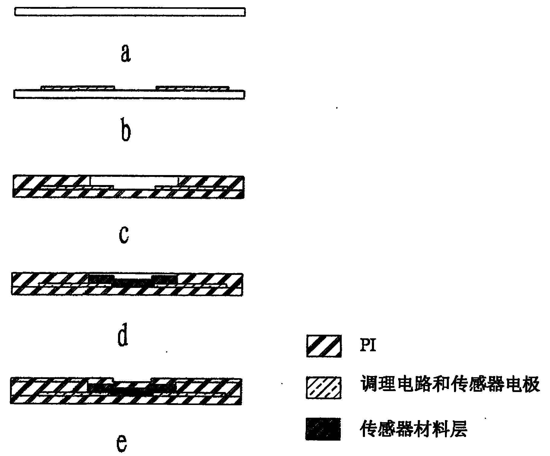
图2是传感器制作过程示意图;Figure 2 is a schematic diagram of the sensor manufacturing process;
图3是传感器材料层的各层示意图;Fig. 3 is each layer schematic diagram of sensor material layer;
图4是传感器的恒温式(CTA)调理电路图。Fig. 4 is the constant temperature (CTA) conditioning circuit diagram of the sensor.
具体实施方式 Detailed ways
本发明的流场传感器,包括在电路板上通过标准的电路板加工工艺制作出的调理电路和电连接至该调理电路的敏感材料层。The flow field sensor of the present invention includes a conditioning circuit manufactured on a circuit board through standard circuit board processing techniques and a sensitive material layer electrically connected to the conditioning circuit.
所述的敏感材料一般可以选择镍或铂或其他适合的材料,其中,敏感材料层既可以是单层敏感材料,也可以是多层复合结构,即由多层敏感材料构成,对于复合结构,各层敏感材料之间的厚度比例可以根据实际需要而确定。复合结构的敏感材料层对本领域技术人员是熟知的,其通常使用铂等稳定性好、抗氧化性强的材料作为最外层,优点是解决了采用诸如镍等敏感材料易氧化的问题,而无论是单层结构还是多层复合结构的敏感材料层,其厚度一般控制在100nm-400nm范围内;The sensitive material generally can be selected from nickel or platinum or other suitable materials, wherein the sensitive material layer can be a single-layer sensitive material, or a multi-layer composite structure, that is, composed of multi-layer sensitive materials, for the composite structure, The thickness ratio between the layers of sensitive materials can be determined according to actual needs. The sensitive material layer of the composite structure is well known to those skilled in the art. It usually uses platinum and other materials with good stability and strong oxidation resistance as the outermost layer. The advantage is that it solves the problem of easy oxidation of sensitive materials such as nickel, while Regardless of whether it is a single-layer structure or a multi-layer composite structure, the thickness of the sensitive material layer is generally controlled within the range of 100nm-400nm;
此外,所述的调理电路类型可以选择恒流式、恒压式或恒温式调理电路,而电路板既可以选择普通的刚性PCB电路板,也可以使用诸如聚酰亚胺等材料制作的柔性电路板。In addition, the type of conditioning circuit can be a constant current, constant voltage or constant temperature conditioning circuit, and the circuit board can be an ordinary rigid PCB circuit board or a flexible circuit made of materials such as polyimide. plate.
为了保护传感器敏感材料层,还可以在传感器敏感材料层上覆盖一层封装层,封装层的材料可以选择聚酰亚胺或陶瓷等,特别是使用柔性电路板时,可以选择聚酰亚胺作为封装层材料。另外,为了增强敏感材料层与电路板基层之间的粘附性,还可以在敏感材料层与所述电路板之间设置由诸如铬等材料形成的粘附层。In order to protect the sensitive material layer of the sensor, a packaging layer can also be covered on the sensitive material layer of the sensor. The material of the packaging layer can be polyimide or ceramics, etc., especially when using a flexible circuit board, polyimide can be selected as encapsulation material. In addition, in order to enhance the adhesion between the sensitive material layer and the base layer of the circuit board, an adhesive layer formed of a material such as chrome may also be provided between the sensitive material layer and the circuit board.
本发明将传感器直接集成在调理电路上,极大地提高了整个系统的集成度,减小了体积和质量,使得这种流场传感器可以很容易的安装在物体表面,而且容易实现流场传感器阵列。同时,随着流场传感器体积的减小,其热容量也随之减小,使得传感器具有较快的响应速度;另外本发明的这种集成的解决方案还降低了整个流场测量系统的功耗。The invention directly integrates the sensor on the conditioning circuit, which greatly improves the integration of the whole system, reduces the volume and quality, makes the flow field sensor can be easily installed on the surface of the object, and it is easy to realize the flow field sensor array . At the same time, as the volume of the flow field sensor decreases, its heat capacity also decreases, so that the sensor has a faster response speed; in addition, this integrated solution of the present invention also reduces the power consumption of the entire flow field measurement system .
下面结合具体实施例对本发明做进一步的解释和说明。图1-图4示出了本发明的流场传感器的一个实施例。本实施例中,如图1a所示,电路板使用由聚酰亚胺材料制作的柔性电路板1,该柔性电路板1上集成有传感器调理电路及其焊盘2和传感器电极对3,同时,如图1b所示,该电路板上还制作有传感器材料层4,其包括粘附层、敏感材料层以及覆盖在敏感材料层之上的封装层,该流场传感器的具体制作过程如图2a-图2e所示,主要包括以下步骤:The present invention will be further explained and illustrated below in conjunction with specific embodiments. 1-4 show an embodiment of the flow field sensor of the present invention. In this embodiment, as shown in Figure 1a, the circuit board uses a
1)首先,在图2a所示的聚酰亚胺柔性电路板1上,使用标准的电路板工艺制作出调理电路和预留的传感器电极对3,如图2b所示,所述传感器电极对3是为了与后面要制作的敏感材料层电连接而准备的,所述传感器电极与所述调理电路电连接;1) At first, on the polyimide
2)然后,如图2c所示,将掩膜板覆盖在上述制作有调理电路和传感器电极的电路板上,采用磁控溅射或真空激光弧沉积技术在两个传感器电极之间及其上依次沉积粘附层和敏感材料层,如图2d所示,粘附层和敏感材料层的结构如图3所示,按照由下至上的次序,依次沉积Cr层、Ni层和Pt层,其中Cr层为粘附层,Ni层和Pt层为敏感材料层,三层的厚度比例Cr∶Ni∶Pt大体上为4∶16∶3,并且敏感材料层的总厚度为100-400nm;2) Then, as shown in Figure 2c, the mask plate is covered on the above-mentioned circuit board with the conditioning circuit and the sensor electrodes, and the magnetron sputtering or vacuum laser arc deposition technology is used to place the mask between and on the two sensor electrodes. The adhesion layer and the sensitive material layer are deposited sequentially, as shown in Figure 2d, the structure of the adhesion layer and the sensitive material layer is shown in Figure 3, and the Cr layer, Ni layer and Pt layer are deposited sequentially in the order from bottom to top, where The Cr layer is an adhesion layer, the Ni layer and the Pt layer are sensitive material layers, the thickness ratio of the three layers Cr:Ni:Pt is generally 4:16:3, and the total thickness of the sensitive material layer is 100-400nm;
3)为了使得电阻具备更加稳定的电阻和温度电阻系数(简称TCR)等特性,优选对传感器进行热处理和电老化。热处理的温度为100-400℃,时间1-4小时;电老化的功率约为传感器的电阻极限功率的60-90%,所述传感器电阻极限功率是指传感器敏感材料层烧毁时的功率值。3) In order to make the resistor have more stable resistance and temperature resistance coefficient (abbreviated as TCR) and other characteristics, it is preferable to perform heat treatment and electrical aging on the sensor. The temperature of the heat treatment is 100-400°C, and the time is 1-4 hours; the power of electrical aging is about 60-90% of the resistance limit power of the sensor, and the resistance limit power of the sensor refers to the power value when the sensitive material layer of the sensor is burned.
4)最后,还可以优选采用蒸镀的方式在整个传感器表面蒸镀一层聚酰亚胺作为封装层,如图2e所示,完成传感器的制作,所述封装层的厚度应尽量薄,以保证传感器的灵敏度。4) Finally, it is also preferable to vapor-deposit a layer of polyimide on the entire surface of the sensor as an encapsulation layer by evaporation, as shown in Figure 2e, to complete the production of the sensor, the thickness of the encapsulation layer should be as thin as possible, so that Ensure the sensitivity of the sensor.
从上述流场传感器的制作过程可以看出,由于本发明利用了标准的电路板工艺制作传感器调理电路和传感器电极,使得传感器的制造过程简单,极大地降低了传感器的制造成本。It can be seen from the manufacturing process of the above-mentioned flow field sensor that since the present invention uses standard circuit board technology to manufacture the sensor conditioning circuit and sensor electrodes, the manufacturing process of the sensor is simple and the manufacturing cost of the sensor is greatly reduced.
热式流场传感器一般有三种工作方式,即恒流式(CCA)、恒压式(CVA)和恒温(阻)式(CTA),其中,恒流和恒压式的调理电路为开环电路,恒温式的调理电路为闭环电路。本实施例流场传感器的调理电路采用恒温式(CTA)调理电路,其原理如图4所示。Thermal flow field sensors generally have three working modes, namely constant current (CCA), constant voltage (CVA) and constant temperature (resistance) (CTA), among them, the conditioning circuits of constant current and constant pressure are open-loop circuits , The thermostatic conditioning circuit is a closed-loop circuit. The conditioning circuit of the flow field sensor in this embodiment adopts a constant temperature (CTA) conditioning circuit, and its principle is shown in FIG. 4 .
该CTA电路由测量电桥、伺服放大器、自动调整环节、输出放大器和输出指示几部分组成。其中,Rw为传感器中传感器材料层的电阻,也称作热膜电阻,其作为电桥的一个桥臂,R1、R2与R3分别为电桥的匹配电阻。其中R1=Rw,R2=R3。加热后的热膜,在受到流速强迫对流作用而造成微小的温度下降(也即传感器材料层的薄膜电阻下降)时,测量电桥能敏感、迅速、稳定、可靠地检测出来,送入伺服放大器进行放大。除电阻Rw外其他桥臂都采用精密电阻,从而保证由电流加热和环境温度变化造成的电阻变化很小。电桥中的RD用来测量热膜电阻冷电阻R0和加过热比Rw/R0用的十进制电阻,其作用是保证传感器材料层能够被控制在预先确定好的工作温度中运转。伺服放大器的功能是将由测量电桥输送来的微弱电信号进行放大,并推动调整环节。自动调整环节主要起电流放大作用,其输出反馈至测量电桥顶端,供给传感器材料层加热电流,保持测量电桥的动态平衡。The CTA circuit is composed of measuring bridge, servo amplifier, automatic adjustment link, output amplifier and output indication. Among them, Rw is the resistance of the sensor material layer in the sensor, also known as thermal film resistance, which is used as a bridge arm of the bridge, and R 1 , R 2 and R 3 are the matching resistances of the bridge respectively. where R 1 =Rw, R 2 =R 3 . When the heated hot film is subjected to the forced convection of the flow rate and causes a slight temperature drop (that is, the film resistance of the sensor material layer drops), the measuring bridge can detect it sensitively, quickly, stably and reliably, and send it to the servo amplifier. to zoom in. Except for the resistance Rw, the other bridge arms are all made of precision resistors, so as to ensure that the resistance changes caused by current heating and ambient temperature changes are small. R D in the bridge is used to measure the cold resistance R 0 of the hot film resistance and the decimal resistance used for the overheating ratio Rw/R 0. Its function is to ensure that the sensor material layer can be controlled to operate at a predetermined working temperature. The function of the servo amplifier is to amplify the weak electrical signal sent by the measuring bridge and push the adjustment link. The automatic adjustment link mainly plays the role of current amplification, and its output is fed back to the top of the measuring bridge to supply the sensor material layer with heating current to maintain the dynamic balance of the measuring bridge.
Rw作为测量电桥的一个桥臂,当流速为零时,电桥平衡,伺服放大器的两个输出端没有电压差,输出指示为零。当传感器材料层在流体的作用下,由强迫对流造成热损耗,其温度tΔ发生变化,由此引起热膜电阻Rw变化,电桥失去平衡,产生一个偏离于平衡点的误差电压。将此误差电压输入到伺服放大器,由高增益的集成运放放大后去推动调整环节,使调整环节反馈到电桥顶端的工作电压能自动升高或降低,也即随之改变热膜的加热电流,使传感器材料层保持恒定的温度,即保持恒定的电阻。桥压的变化也就反映了流速的变化。与此同时,将桥压输入到输出放大器,经与基准电压比较,将其差值放大作为输出指示。利用单个传感器可测量单点风速/剪应力。Rw is used as a bridge arm of the measuring bridge. When the flow rate is zero, the bridge is balanced, there is no voltage difference between the two output terminals of the servo amplifier, and the output indicator is zero. When the sensor material layer is under the action of fluid, heat loss is caused by forced convection, and its temperature t Δ changes, which causes the thermal film resistance Rw to change, and the bridge loses balance, generating an error voltage that deviates from the equilibrium point. Input this error voltage to the servo amplifier, which is amplified by the high-gain integrated operational amplifier to drive the adjustment link, so that the adjustment link can automatically increase or decrease the working voltage fed back to the top of the bridge, that is, the heating of the hot film will be changed accordingly. An electric current keeps the layer of sensor material at a constant temperature, i.e. at a constant resistance. Changes in bridge pressure reflect changes in flow velocity. At the same time, the bridge voltage is input to the output amplifier, and compared with the reference voltage, the difference is amplified as an output indicator. Single point wind speed/shear stress can be measured with a single sensor.
对本实施例制作的流场传感器进行测量,可得到其响应时间小于1s(商业化的热膜传感器Pt100的响应时间1~9s);而单个传感器的面积只有5×1mm2(厚度极其微小),质量也只有0.01g,便于阵列化。The flow field sensor made in this embodiment is measured, and its response time can be found to be less than 1s (the response time of the commercialized hot film sensor Pt100 is 1-9s); while the area of a single sensor is only 5 ×1mm2 (thickness is extremely small), The mass is only 0.01g, which is convenient for arraying.
如果将多个流场传感器布置成阵列,还能够测得物体表面的流场分布情况,这对本领域技术人员是熟知的。If a plurality of flow field sensors are arranged in an array, the flow field distribution on the surface of the object can also be measured, which is well known to those skilled in the art.
最后应说明的是,以上各附图中的实施例仅用以说明本发明的流场传感器结构及其制作方法,但非限制。尽管参照实施例对本发明进行了详细说明,本领域的普通技术人员应当理解,对本发明的技术方案进行各种组合、修改或者等同替换,都不脱离本发明技术方案的精神和范围,其均应涵盖在本发明的权利要求范围当中。Finally, it should be noted that the embodiments in the above figures are only used to illustrate the structure and manufacturing method of the flow field sensor of the present invention, but are not limiting. Although the present invention has been described in detail with reference to the embodiments, those skilled in the art should understand that various combinations, modifications or equivalent replacements of the technical solutions of the present invention will not depart from the spirit and scope of the technical solutions of the present invention, and all should be fall within the scope of the claims of the present invention.
Claims (10)
Priority Applications (1)
| Application Number | Priority Date | Filing Date | Title |
|---|---|---|---|
| CN200810115672A CN101614753A (en) | 2008-06-26 | 2008-06-26 | Flow field sensor and manufacturing method thereof |
Applications Claiming Priority (1)
| Application Number | Priority Date | Filing Date | Title |
|---|---|---|---|
| CN200810115672A CN101614753A (en) | 2008-06-26 | 2008-06-26 | Flow field sensor and manufacturing method thereof |
Publications (1)
| Publication Number | Publication Date |
|---|---|
| CN101614753A true CN101614753A (en) | 2009-12-30 |
Family
ID=41494505
Family Applications (1)
| Application Number | Title | Priority Date | Filing Date |
|---|---|---|---|
| CN200810115672A Pending CN101614753A (en) | 2008-06-26 | 2008-06-26 | Flow field sensor and manufacturing method thereof |
Country Status (1)
| Country | Link |
|---|---|
| CN (1) | CN101614753A (en) |
Cited By (8)
| Publication number | Priority date | Publication date | Assignee | Title |
|---|---|---|---|---|
| CN102370476A (en) * | 2011-09-28 | 2012-03-14 | 上海交通大学 | Cardiovascular blood flow velocity sensor |
| CN104523276A (en) * | 2014-12-23 | 2015-04-22 | 清华大学 | Respiration monitoring nasal paste and respiratory airflow monitoring system |
| CN106066407A (en) * | 2016-06-22 | 2016-11-02 | 西华大学 | A kind of near wall flow rate measuring device |
| CN108593956A (en) * | 2018-04-28 | 2018-09-28 | 中国空气动力研究与发展中心超高速空气动力研究所 | Micro- current meter of double mode and preparation method thereof |
| CN112129969A (en) * | 2020-09-17 | 2020-12-25 | 青岛芯笙微纳电子科技有限公司 | Miniature anemometer |
| CN113418675A (en) * | 2021-08-06 | 2021-09-21 | 中国空气动力研究与发展中心设备设计与测试技术研究所 | Hot wire measurement wind tunnel flow field disturbance modal method |
| CN115219056A (en) * | 2022-07-18 | 2022-10-21 | 山东大学 | Quick-response and high-temperature-resistant film type temperature sensor and preparation method thereof |
| CN116222658A (en) * | 2023-02-03 | 2023-06-06 | 国网湖北省电力有限公司超高压公司 | A multifunctional sensing device and fusion method for UHV substation frame monitoring |
-
2008
- 2008-06-26 CN CN200810115672A patent/CN101614753A/en active Pending
Cited By (11)
| Publication number | Priority date | Publication date | Assignee | Title |
|---|---|---|---|---|
| CN102370476A (en) * | 2011-09-28 | 2012-03-14 | 上海交通大学 | Cardiovascular blood flow velocity sensor |
| CN102370476B (en) * | 2011-09-28 | 2013-07-10 | 上海交通大学 | Cardiovascular blood flow velocity sensor |
| CN104523276A (en) * | 2014-12-23 | 2015-04-22 | 清华大学 | Respiration monitoring nasal paste and respiratory airflow monitoring system |
| CN106066407A (en) * | 2016-06-22 | 2016-11-02 | 西华大学 | A kind of near wall flow rate measuring device |
| CN108593956A (en) * | 2018-04-28 | 2018-09-28 | 中国空气动力研究与发展中心超高速空气动力研究所 | Micro- current meter of double mode and preparation method thereof |
| CN108593956B (en) * | 2018-04-28 | 2023-06-02 | 中国空气动力研究与发展中心超高速空气动力研究所 | Dual-mode micro-flowmeter and preparation method thereof |
| CN112129969A (en) * | 2020-09-17 | 2020-12-25 | 青岛芯笙微纳电子科技有限公司 | Miniature anemometer |
| CN113418675A (en) * | 2021-08-06 | 2021-09-21 | 中国空气动力研究与发展中心设备设计与测试技术研究所 | Hot wire measurement wind tunnel flow field disturbance modal method |
| CN115219056A (en) * | 2022-07-18 | 2022-10-21 | 山东大学 | Quick-response and high-temperature-resistant film type temperature sensor and preparation method thereof |
| CN115219056B (en) * | 2022-07-18 | 2024-09-03 | 山东大学 | A fast-response and high-temperature-resistant thin-film temperature sensor and a method for preparing the same |
| CN116222658A (en) * | 2023-02-03 | 2023-06-06 | 国网湖北省电力有限公司超高压公司 | A multifunctional sensing device and fusion method for UHV substation frame monitoring |
Similar Documents
| Publication | Publication Date | Title |
|---|---|---|
| CN101614753A (en) | Flow field sensor and manufacturing method thereof | |
| KR101489104B1 (en) | Electric element | |
| CN100582784C (en) | Micro-mechanical two-dimension wind speed and wind direction sensor and signal processing circuit thereof | |
| CN110864736B (en) | Flexible sensor strain and temperature compensation method and multi-sensing integrated sensor | |
| JPH0257853B2 (en) | ||
| CN110174527A (en) | A kind of hot type fiber grating wind speed wind direction sensor and detection method | |
| JP5590460B2 (en) | Dew point measuring device and gas characteristic measuring device | |
| CN104482971A (en) | Thermal flow sensor on basis of MEMS (micro-electromechanical systems) technology | |
| JP5769043B2 (en) | Electrical device, integrated device, electronic circuit and temperature calibration device | |
| CN109211342B (en) | Airflow flowmeter, MEMS silicon-based temperature-sensitive chip and preparation method thereof | |
| JP5590459B2 (en) | Dew point measuring device and gas characteristic measuring device | |
| CN115235729B (en) | A high temporal and spatial resolution temperature sensor for simultaneous measurement of oriented and normal heat flux | |
| CN107830967B (en) | A kind of MEMS air differential pressure sensor | |
| CN113551813A (en) | Integrated temperature control micro-miniature silicon piezoresistive pressure sensor and manufacturing method thereof | |
| RU2312319C2 (en) | Thin-film pressure gage | |
| CN215984954U (en) | Integrated temperature control micro-miniature silicon piezoresistive pressure sensor | |
| CN113091940B (en) | Heating and temperature measuring integrated wind speed and direction sensor | |
| JP5761589B2 (en) | Electrical device, integrated device, electronic circuit and temperature calibration device | |
| JP2019138780A (en) | Heat type flow sensor | |
| CN115078843A (en) | Temperature compensation type on-chip integrated conductivity sensor and conductivity measurement method | |
| JPH09318412A (en) | Thermal flow sensor | |
| Stanimirović et al. | Pt Resistive Film Sensors | |
| RU215318U1 (en) | Thermal gas flow sensor of calorimetric type | |
| CN223435632U (en) | A double-sided asymmetric integrated structure thin film resistance thermal flow sensor | |
| SU613219A1 (en) | Semiconductor pressure pickup |
Legal Events
| Date | Code | Title | Description |
|---|---|---|---|
| C06 | Publication | ||
| PB01 | Publication | ||
| C10 | Entry into substantive examination | ||
| SE01 | Entry into force of request for substantive examination | ||
| C12 | Rejection of a patent application after its publication | ||
| RJ01 | Rejection of invention patent application after publication |
Application publication date: 20091230 |