[go: up one dir, main page]

CN101605429B - Method for machining rigid-flexible combination plate needing to be stamped and special die - Google Patents

Method for machining rigid-flexible combination plate needing to be stamped and special die Download PDF

Info

Publication number
CN101605429B
CN101605429B CN2009101085665A CN200910108566A CN101605429B CN 101605429 B CN101605429 B CN 101605429B CN 2009101085665 A CN2009101085665 A CN 2009101085665A CN 200910108566 A CN200910108566 A CN 200910108566A CN 101605429 B CN101605429 B CN 101605429B
Authority
CN
China
Prior art keywords
rigid
flex
height
combined board
difference
Prior art date
Legal status (The legal status is an assumption and is not a legal conclusion. Google has not performed a legal analysis and makes no representation as to the accuracy of the status listed.)
Expired - Fee Related
Application number
CN2009101085665A
Other languages
Chinese (zh)
Other versions
CN101605429A (en
Inventor
黄道明
严永亮
王勇恩
唐慧
Current Assignee (The listed assignees may be inaccurate. Google has not performed a legal analysis and makes no representation or warranty as to the accuracy of the list.)
SHENZHEN HUALIN CIRCUIT TECHNOLOGY Co Ltd
Original Assignee
Shenzhen Huada Electric Circuit Technology Co ltd
Priority date (The priority date is an assumption and is not a legal conclusion. Google has not performed a legal analysis and makes no representation as to the accuracy of the date listed.)
Filing date
Publication date
Application filed by Shenzhen Huada Electric Circuit Technology Co ltd filed Critical Shenzhen Huada Electric Circuit Technology Co ltd
Priority to CN2009101085665A priority Critical patent/CN101605429B/en
Publication of CN101605429A publication Critical patent/CN101605429A/en
Application granted granted Critical
Publication of CN101605429B publication Critical patent/CN101605429B/en
Expired - Fee Related legal-status Critical Current
Anticipated expiration legal-status Critical

Links

Images

Landscapes

  • Structure Of Printed Boards (AREA)

Abstract

一种需冲型的刚挠结合板的加工方法及专用模具,需要冲型出的产品在刚挠结合部分与挠性部分之间存在较大的高度差,该高度差为≥0.2mm,当冲型需冲切到刚挠结合部与挠性部分的交界处,则在冲型之前,于模具的下模(40)上设置一个可适配到挠性部分(30)、垫住挠性部分下表面(301)的凸起(41),所述凸起的高度等于所述高度差。这样消除了模具冲到的高度差,冲切透彻,避免撕裂,提高了产品的良率,且工作性能稳定可靠,成本低廉,适用范围较为广泛,当高度差大于或等于0.2mm时可采用。

Figure 200910108566

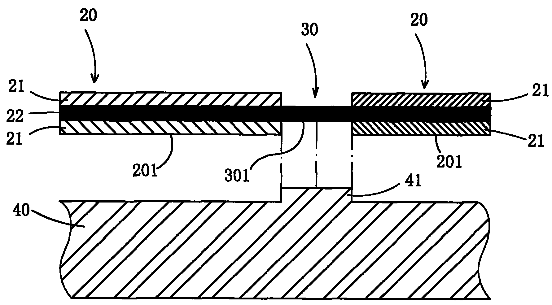
A processing method and special mold for a rigid-flexible plate that needs to be punched. There is a large height difference between the rigid-flexible part and the flexible part of the product that needs to be punched out. The height difference is ≥ 0.2mm. The punching shape needs to be punched to the junction of the rigid-flexible part and the flexible part. Before punching the shape, set a flexible part (30) on the lower die (40) of the mold to cushion the flexible part (30). A protrusion (41) on part of the lower surface (301), the height of the protrusion is equal to the height difference. In this way, the height difference of the die punching is eliminated, the punching is thorough, the tearing is avoided, the yield rate of the product is improved, and the working performance is stable and reliable, the cost is low, and the scope of application is relatively wide. When the height difference is greater than or equal to 0.2mm, it can be used .

Figure 200910108566

Description

A kind of processing method and particular manufacturing craft that needs the rigid-flex combined board of stamp
Technical field
The present invention relates to the processing molding method of rigid-flexible combined circuit plate, relate in particular to a kind of processing method and particular manufacturing craft that has the rigid-flex combined board that needs stamp of difference in height.
Background technology
Rigid-flex combined board is as a kind of special electronic interconnection technology; Can reduce electronic product package size, weight, avoid Miswire; Realize the three-dimensional assembling under the different assembled conditions; And have light, thin, short, little, structure flexible characteristic, be widely used in computer, aviation electronics, Military Electronic Equipment, mobile phone, DV, Communication Equipment, the analytical instrument.The U.S. is very ripe with rigid-flex combined board on military and space science, and mostly the number of plies is 6,8,10 layers.Korea S PCB manufacturer is in the technical maturation the most of rigid-flex combined board at present, and other regional manufacturers are stepping up the research and development to rigid-flex combined board technology now.Rigid-flex combined board from now on can more field, especially consumer fields that are used to reduce encapsulation more.Rigid-flex combined board is by rigidity and flexible substrate is laminated together selectively forms, and structure is tight, forms or conduction connects with plated-through hole; One or more rigid regions and one or more flexible region are arranged on the every rigid-flex combined board, and it has made full use of the characteristics of flex plate, and has solved the problem that is electrically connected with rigid plate; Can three-dimensionally install, effectively utilize installing space, reduce installation cost; And alternative plug-in unit; Guarantee the reliability under environment such as impact, humidity, but its manufacture difficulty is high, a cost height.The technological difficulties of rigid-flex combined board in manufacturing process mainly contain: the dimensional stability technology of rigid-flexible combined printed wiring board, the elastic adhesive technology of rigid-flexible combined printed wiring board, the forming technique of rigid-flexible combined printed wiring board etc.
In the time of will the rigid-flex combined board that tack coat presses being used mould to carry out punching molding as the circuit board shape of needs; There is a difference in height in intersection at rigid-flexible bound fraction and flex section; If design according to the circuit board of routine; Find in the practice, at this bigger difference in height place of rigid-flex combined board (>=0.2mm), regular meeting tears flex section or leaves over and dash the flex section that does not cut through during stamp; Cause the flex section of product to tear at die-cut place easily when separating product and waste material, thereby cause scrapping of product with external force (such as staff).
Summary of the invention
The technical problem that the present invention will solve is; The processing method and the particular manufacturing craft thereof of the rigid-flex combined board that needs stamp are provided; When the intersection punching molding of rigid-flexible bound fraction that has difference in height and flex section; Guarantee can not cause flex section to tear behind die-cut thorough, the rigid-flex combined board stamp, to improve the yield in the rigid-flex combined board course of processing.
For solving the problems of the technologies described above; The present invention provides a kind of processing method that needs the rigid-flex combined board of stamp, and the shape of product that needs stamp to go out has determined to be die-cut to the intersection of rigid-flexible bound fraction and flex section, and the lower surface of the rigid-flexible bound fraction of said intersection is lower than the lower surface of flex section; There is difference in height; It is characterized in that, when said difference in height during more than or equal to 0.2mm, before the stamp; On the counterdie of mould, be provided with one and can be fitted to the firmly convexity of flex section lower surface of flex section, pad, the height of said convexity equals said difference in height.
Said convexity and counterdie are as a whole.
Said rigid-flex combined board comprises flex plate, and the top and following tack coat respectively of the subregion of this flex plate is pressed with the rigid plate of thickness more than or equal to 0.2mm, thereby forms rigid-flexible bound fraction, and the remainder of this flex plate is a flex section.
Said flex plate thickness is 0.1mm, and said rigid plate thickness is 0.35mm.
The present invention also provides a kind of particular manufacturing craft that is used for the processing method of the said rigid-flex combined board that needs stamp; Constitute by upper die and lower die; It is characterized in that; A convexity that can be fitted to flex section, the flex section pad is lived is set on said counterdie, and the lower surface that the height of said convexity equals the corresponding flex section of high spot is higher than the difference in height of the lower surface of said rigid-flexible bound fraction, and said difference in height is more than or equal to 0.2mm.
Said difference in height is 0.35mm.
Said convexity and counterdie are as a whole.
Beneficial effect of the present invention is: need the rigid-flexible bound fraction and the flex section of the product that stamp goes out that bigger difference in height is arranged, because the present invention before stamp, forms boss with the lower corresponding to flex section on the mould; Pad is lived the lower surface of flex section; Thereby eliminated the difference in height that mould is flushed to, the applicant experiment showed, that in a large number the flex section of big difference in height when die-cut like this is difficult for tearing; Die-cut thorough; Avoided not passing through the flex section that causes at the place and torn, therefore improved the yield of product, for the Precision Machining of rigid-flex combined board has been established solid foundation with the manpower separate die-cut.And stable and reliable working performance; With low cost, the scope of application is comparatively extensive, when the difference in height of the rigid-flexible bound fraction of said intersection and flex section can adopt during more than or equal to 0.2mm; On mould, form the boss more than or equal to 0.2, mold machining technology can reach.
Description of drawings
Below in conjunction with accompanying drawing and embodiment the present invention is done further detailed description.
Fig. 1 is the shape of product schematic top plan view that the present invention treats the rigid-flex combined board and the need stamp of stamp processing.
Fig. 2 is the A-A cross-sectional schematic of Fig. 1.
Fig. 3 is the cross-sectional schematic that rigid-flex combined board combines with mould.
Embodiment
Like Fig. 1, Fig. 2 is rigid-flex combined board of the present invention; With four layers of rigid-flex combined board is example, and this rigid-flex combined board has a flex plate 22, and thickness can be 0.10mm; Posted insulating barrier (not marking among the figure) on the flex plate; Top and the following adhesive layer that adopts respectively of the both sides of this flex plate is pressed with the rigid plate 21 of thickness more than or equal to 0.2mm, and rigid plate thickness is 0.35mm in the present embodiment, thereby forms rigid-flexible bound fraction 20 in both sides; The mid portion of this flex plate 22 does not have rigid plate, is flex section 30.The number of plies of the rigid-flex combined board of here enumerating does not constitute the restriction to technical scheme, as long as the lower surface 201 of rigid-flexible bound fraction 20 is lower than the lower surface 301 of flex section 30, forms more than or equal to the 0.2mm difference in height.In the present embodiment, this difference in height is the thickness of the rigid plate of flex plate lower surface subsides, is 0.35mm.
Be depicted as the shape of product 10 that needs stamp to go out with mould like Fig. 1 dotted line, there is difference in height 0.35mm in this product between the lower surface of rigid-flexible bound fraction and flex section, and this difference in height is bigger, more than or equal to 0.2mm.As shown in Figure 3, in this embodiment, before the stamp; (form at mould by upper die and lower die; Patrix is not shown) counterdie 40 on be provided with one can be fitted to flex section 30, with the convexity 41 that flex section lower surface pad is lived, the height of said convexity equals described difference in height, equals the thickness 0.35 of the rigid plate that the flex section lower surface pastes in the present embodiment; As optimized technical scheme, said protruding 41 whole formation on counterdie 40.Like this, after stamp the time, the flex section of having avoided causing because of said difference in height dashes and does not cut through and tear.

Claims (7)

1. the processing method of the rigid-flex combined board of a need stamp; The shape of product (10) that needs stamp to go out has determined to be die-cut to the intersection of rigid-flexible bound fraction (20) and flex section (30); The lower surface (201) of the rigid-flexible bound fraction (20) of said intersection is lower than the lower surface (301) of flex section (30), has difference in height, it is characterized in that; When said difference in height during more than or equal to 0.2mm; Before the stamp, on the counterdie (40) of mould, be provided with one and can be fitted to the firmly convexity (41) of flex section lower surface (301) of flex section (30), pad, the height of said convexity equals said difference in height.
2. the processing method that needs the rigid-flex combined board of stamp according to claim 1 is characterized in that said convexity (41) is as a whole with counterdie (40).
3. the processing method that needs the rigid-flex combined board of stamp according to claim 1; It is characterized in that; Said rigid-flex combined board comprises flex plate (22); Top and the following tack coat respectively of the subregion of this flex plate is pressed with the rigid plate (21) of thickness more than or equal to 0.2mm, thereby forms rigid-flexible bound fraction (20), and the remainder of this flex plate (22) is flex section (30).
4. the processing method that needs the rigid-flex combined board of stamp according to claim 3 is characterized in that said flex plate (22) thickness is 0.1mm, and said rigid plate (21) thickness is 0.35mm.
5. particular manufacturing craft that is used for the processing method of the said rigid-flex combined board that needs stamp of claim 1; Constitute by upper die and lower die; It is characterized in that; A convexity (41) that can be fitted to flex section (30), the flex section pad is lived is set on said counterdie (40), and the lower surface (31) that the height of said convexity equals the corresponding flex section of high spot (30) is higher than the difference in height of the lower surface (21) of said rigid-flexible bound fraction (20), and said difference in height is more than or equal to 0.2mm.
6. the particular manufacturing craft of the processing method of the rigid-flex combined board of need stamp according to claim 5 is characterized in that said difference in height is 0.35mm.
7. the particular manufacturing craft of the processing method of the rigid-flex combined board of need stamp according to claim 5 is characterized in that said convexity (41) is as a whole with counterdie (40).
CN2009101085665A 2009-07-01 2009-07-01 Method for machining rigid-flexible combination plate needing to be stamped and special die Expired - Fee Related CN101605429B (en)

Priority Applications (1)

Application Number Priority Date Filing Date Title
CN2009101085665A CN101605429B (en) 2009-07-01 2009-07-01 Method for machining rigid-flexible combination plate needing to be stamped and special die

Applications Claiming Priority (1)

Application Number Priority Date Filing Date Title
CN2009101085665A CN101605429B (en) 2009-07-01 2009-07-01 Method for machining rigid-flexible combination plate needing to be stamped and special die

Publications (2)

Publication Number Publication Date
CN101605429A CN101605429A (en) 2009-12-16
CN101605429B true CN101605429B (en) 2012-01-25

Family

ID=41470907

Family Applications (1)

Application Number Title Priority Date Filing Date
CN2009101085665A Expired - Fee Related CN101605429B (en) 2009-07-01 2009-07-01 Method for machining rigid-flexible combination plate needing to be stamped and special die

Country Status (1)

Country Link
CN (1) CN101605429B (en)

Families Citing this family (1)

* Cited by examiner, † Cited by third party
Publication number Priority date Publication date Assignee Title
CN113910366A (en) * 2021-10-08 2022-01-11 苏州淏源精密科技有限公司 Punching die and punching method for rigid-flex board

Citations (4)

* Cited by examiner, † Cited by third party
Publication number Priority date Publication date Assignee Title
JPH07135393A (en) 1993-11-11 1995-05-23 Mitsubishi Gas Chem Co Inc Rigid flexible multilayer printed board
KR20050045652A (en) * 2003-11-12 2005-05-17 삼성전기주식회사 External form processing method of the rigid flexible pcb
CN1765161A (en) * 2003-04-18 2006-04-26 揖斐电株式会社 Rigid-flex wiring board
CN1806474A (en) * 2004-06-11 2006-07-19 揖斐电株式会社 Rigid-flex circuit board and manufacturing method thereof

Patent Citations (4)

* Cited by examiner, † Cited by third party
Publication number Priority date Publication date Assignee Title
JPH07135393A (en) 1993-11-11 1995-05-23 Mitsubishi Gas Chem Co Inc Rigid flexible multilayer printed board
CN1765161A (en) * 2003-04-18 2006-04-26 揖斐电株式会社 Rigid-flex wiring board
KR20050045652A (en) * 2003-11-12 2005-05-17 삼성전기주식회사 External form processing method of the rigid flexible pcb
CN1806474A (en) * 2004-06-11 2006-07-19 揖斐电株式会社 Rigid-flex circuit board and manufacturing method thereof

Also Published As

Publication number Publication date
CN101605429A (en) 2009-12-16

Similar Documents

Publication Publication Date Title
JP5349428B2 (en) Electronic element built-in type printed circuit board and manufacturing method thereof
CN101686604B (en) Flexible printed circuit whole board punching method
CN101600306B (en) Method for processing stamped rigid-flexible board and rigid-flexible board
US20100175242A1 (en) Method for packaging micro electromechanical systems microphone
CN109429443A (en) The production method of rigid-flexible circuit board
CN102497746B (en) The manufacture method of circuit board
WO2009037833A1 (en) Solid printed wiring board, method for manufacturing solid printed wiring board, and electronic component module
CN102387662A (en) Rigid-flexibility circuit board and manufacturing method thereof
CN101472393A (en) Stamping mold for flexible circuit board
CN101605429B (en) Method for machining rigid-flexible combination plate needing to be stamped and special die
CN105101674A (en) Manufacturing method of stacked circuit board and stacked circuit board
CN204031568U (en) Flexible printed circuit board
CN201157868Y (en) Flexible circuit board stamping die
JP4033157B2 (en) Conducting path forming method
CN100527916C (en) Multi-layer flexible circuit board and its producing method
CN201418206Y (en) PCB jointed board with stamp hole
CN106304698B (en) A kind of method for manufacturing circuit board
CN103732008B (en) Connecting sheet circuit board and the manufacture method of connecting sheet circuit board
CN102458035B (en) Structure of slotting printed board
CN108055773A (en) A kind of soft or hard combination flexible PCB and its manufacturing method
CN202335060U (en) Single-faced double-contact flexible circuit board
CN106886815A (en) A kind of miniature hyperfrequency anti-metal electronic tag and preparation method thereof
US11461609B1 (en) Multilayer structure and method of manufacturing such
CN204031569U (en) A kind of flexible printed circuit board
CN108016103A (en) A kind of pen electricity camera module conducting resinl

Legal Events

Date Code Title Description
C06 Publication
PB01 Publication
C10 Entry into substantive examination
SE01 Entry into force of request for substantive examination
C53 Correction of patent of invention or patent application
CB03 Change of inventor or designer information

Inventor after: Huang Daoming

Inventor after: Yan Yongliang

Inventor after: Wang Yongen

Inventor after: Tang Hui

Inventor before: Yan Yongliang

Inventor before: Wang Yongen

Inventor before: Tang Hui

COR Change of bibliographic data

Free format text: CORRECT: INVENTOR; FROM: YAN YONGLIANG WANG YONGEN TANG HUI TO: HUANG DAOMING YAN YONGLIANG WANG YONGEN TANG HUI

C14 Grant of patent or utility model
GR01 Patent grant
ASS Succession or assignment of patent right

Owner name: SHENZHEN HUALIN CIRCUIT TECHNOLOGY CO., LTD.

Free format text: FORMER OWNER: SHENZHEN HUADA CIRCUIT SCIENCE + TECHNOLOGY CO., LTD.

Effective date: 20130809

C41 Transfer of patent application or patent right or utility model
TR01 Transfer of patent right

Effective date of registration: 20130809

Address after: No. 1 Longgang District of Shenzhen City, Guangdong province 518217 Baolong Industrial City Jinlong Avenue

Patentee after: Shenzhen Hualin Circuit Technology Co., Ltd.

Address before: No. 1 Longgang District of Shenzhen City, Guangdong province 518217 Baolong Industrial City Jinlong Avenue

Patentee before: Shenzhen Huada Circuit Science & Technology Co., Ltd.

CF01 Termination of patent right due to non-payment of annual fee

Granted publication date: 20120125

Termination date: 20190701

CF01 Termination of patent right due to non-payment of annual fee