Summary of the invention
In view of this, the embodiment of the invention proposes processing unit, method and the decoder of reference frame in a kind of image, realizes that by hardware reference frame reorders, than the very big speed up processing of prior art.
Described processing unit comprises control circuit (301), address pointer register (302), insertion position register (303), comparator (304), reference frame lists memory cell (305) and position and logical calculated device (308);
Described control circuit (301) is used for according to the syntax elements startup or finishes to reorder service logic, and the service logic that reorders comprises: send the initialization enable information to address pointer register (302), insertion position register (303) and reference frame lists memory cell (305); Calculate the reference frame sequence number that needs reorder according to syntax elements frame number absolute offset values or long-term frame number, and the shift enable signal that will export address pointer register (302) to is changed to effectively; If receive equal marking signal from comparator (304), it is invalid that the shift enable signal that then will output to address pointer register (302) is changed to, and the reference frame sequence number that needs reorder is sent to reference frame lists memory cell (305), send to reference frame lists memory cell (305) and upgrade index signal; After reference frame lists memory cell (305) is finished renewal, send shift enable signal to insertion position register (303);
Address pointer register (302) bit wide is the M bit, link to each other with reference frame lists memory cell (305), register value is represented the address pointer of the reference frame register in the reference frame lists memory cell (305), when the initialization enable information of receiving from control circuit (301), then each of register value all is set to 0; When receiving that the shift enable signal from control circuit (301) is effective, clock cycle of then every mistake moves to right 1 with register value, and mends 1 in a high position; Described M is the natural number greater than 2;
Insertion position register (303) bit wide is the M bit, links to each other with reference frame lists memory cell (305), when the initialization enable information of receiving from control circuit (301), then each of register value all is set to 1; When the shift enable signal received from control circuit (301), then register value is moved to right 1, and mend 0 in a high position;
The reference frame sequence number that comparator (304) is used in the reference frame register of the reference frame lists memory cell (305) that will point to from the address pointer that the reference frame sequence number that reorders of needs of control circuit (301) and the register value of address pointer register (302) are represented compares, and sends equal marking signal if both equate to control circuit (301);
Position and logical calculated device (308), its input is link address pointer register (302) and insertion position register (303) respectively, the position is connected reference frame lists memory cell (305) with the output of logical calculated device (308), be used for the register value of the register value of address pointer register (302) and insertion position register (303) is carried out position and operation, the operating result of position and logical calculated device (308) is as the positional information of the reference frame register of needs renewal;
Reference frame lists memory cell (305) comprises M reference frame register and register read writing controller (309), and each reference frame register is respectively applied for deposits a reference frame sequence number; The reference frame sequence number that the reference frame register that the address pointer that reference frame lists memory cell (305) is used for that the register value of address pointer register (302) is represented points to is stored exports comparator (304) to; When receiving that renewal index signal from control circuit (301) is effective, positional information according to position and logical calculated device (308) output, the address pointer sensing position reference frame register afterwards that the register value of insertion position register (303) is represented is done the order displacement to the register value of the reference frame register of address pointer register 302 address pointers sensing, described order displacement is for to store the register value in n-1 the reference frame register in n the reference frame register into, the n value is a natural number, 1≤n≤M will be received from reference frame sequence number that the needs of control circuit (301) reorder then and deposit in the reference frame register that address pointer that the register value of described insertion position register (303) represents points to.
The processing method of reference frame in the described image adopts aforementioned means to realize, comprises the steps:
A, before every frame decoding, each of the register value of address pointer register (302) all is set to 0, each of the register value of insertion position register (303) all is set to 1, and initialization reference frame lists memory cell (305);
The syntax elements reference frame lists of judging B, control circuit (301) reorders indicates whether be 1, if then calculate the reference frame sequence number that needs reorder according to syntax elements absolute reference frame number side-play amount or long-term frame number, and continue execution in step C, otherwise return steps A;
The shift enable signal that C, control circuit (301) will export address pointer register (302) to is changed to effectively, and the register value of each clock cycle with address pointer register (302) moves to right one, and mends 1 in a high position; The reference frame sequence number that the register value of the reference frame register in the reference frame lists memory cell (305) that the address pointer that comparator (304) is represented the register value of address pointer register (302) points to and the needs that described control circuit (301) obtains reorder compares, if both equate, then equate marking signal to control circuit (301) output;
It is invalid that the shift enable signal that D, control circuit (301) will output to address pointer register (302) is changed to, and the reference frame sequence number that needs reorder is sent to reference frame lists memory cell (305), send to reference frame lists memory cell (305) and upgrade index signal;
The content of the reference frame register that the address pointer that the address pointer sensing position reference frame register afterwards that E, reference frame lists memory cell (305) are represented the register value of insertion position register (303) is represented to the register value of address pointer register (302) points to is done the order displacement, and described order is shifted to the register value in n-1 the reference frame register is deposited in n the reference frame register; N is a natural number, 1≤n≤M, M is the sum of reference frame register, will be received from reference frame sequence number that the needs of control circuit (301) reorder then and deposit in the reference frame register that address pointer that the register value of insertion position register (303) represents points to;
F, reference frame lists memory cell (305) obtain the positional information that needs the reference frame register that upgrades from address pointer register (302) and insertion position register (303), and insertion position register (303) moves to right 1 with register value, and mends 0 in a high position;
G, control circuit (301) judge whether the reorder value of indication of syntax elements frame number is 3, then goes to step C if not, if then finish the reference frame flow process that reorders.
The decoder that the embodiment of the invention proposes comprises the processing unit of reference frame in the earlier figures picture, in order to realize that reference frame reorders.
As can be seen from the above technical solutions, the present invention program realizes that by hardware reference frame reorders, and very big speed up processing is applicable to the needs of HD video technical development more.
Embodiment
For making the purpose, technical solutions and advantages of the present invention clearer, the present invention is further elaborated below in conjunction with accompanying drawing.
Before technical solution of the present invention is elaborated, at first introduce the algorithm implementation procedure that reference frame reorders.Reference frame reorders and specifically comprises following process:
Initialization procedure: decoder need carry out the initialization ordering to reference frame before each P_Slice is decoded.Wherein, reference frame is divided into two kinds of short-term reference frame and long term reference frames again, short-term reference frame uses reference frame sequence number (frame_num) to arrange according to descending, the reference frame of frame number maximum ranks the first, promptly come the 1st, and call number (ref_idx) 0 is distributed to this frame from the nearest forward reference frame of present frame; And long term reference frame is arranged according to the ascending order of the long-term picture numbers of parameter (LongTermPicNum).In reference frame lists, all short-term reference frame are before long term reference frame.
Process reorders: in decoding P_Slice process, if the value of syntax elements reference frame lists record mark 10 (ref_pic_list_reordering_flag_l0) is 1, then need to carry out reordering of reference frame lists.The benefit that reorders is then can reduce transmission code stream if when the bigger reference frame of a call number (ref_idx) is frequently quoted, this frame is put into the prostatitis of reference frame lists, thereby makes its call number less.The process of reordering relates generally to four syntax elements: the reference frame lists sign (ref_pic_list_reordering_flag_l0) that reorders, the frame number indication (reordering_of_pic_num_idc) of reordering, frame number absolute offset values (abs_diff_pic_num_minus1) and long-term frame number (long_term_pic_num).The description of use of each syntax elements is as follows:
When syntax elements ref_pic_list_reordering_flag_l0 was 1, expression need be carried out reordering of reference frame, and syntax elements reordering_of_pic_num_idc is used to represent the method that reorders and whether finishes the process of reordering.Abs_diff_pic_num_minus1 or long_term_pic_num are used for then representing that in the reference picture which will be reallocated call number (ref_idx).Table 1 has provided the value of reordering_of_pic_num_idc and the relation between the method for reordering.
Table 1
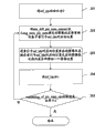
The algorithm realization flow of the process that reorders comprises the steps: as shown in Figure 2
Step 201: ref_idx is initialized as 0.
Step 202: the position that the image of abs_diff_pic_num_minus1 or Long_term_pic_num appointment is placed on call number ref_idx correspondence in the reference frame lists.
Step 203: image that the position of call number ref_idx correspondence is original and the image that comes after the position of call number ref_idx correspondence thereof move a picture position to the tabulation rear portion successively.
Step 204: ref_idx is added 1.
Step 205: whether the value of judging reordering_of_pic_num_idc equals 3, if, then finish sequencer procedure, otherwise, go to step 202 repeating step 202-204.
The embodiment of the invention proposes the processing unit of reference frame in a kind of image, as shown in Figure 3, mainly comprises following components: control circuit 301, address pointer register 302, insertion position register 303, comparator 304, reference frame lists memory cell 305.In addition, also have control interface 306 and the initial reference frame list information input interface 307 relevant with this processing unit.Wherein, the bit wide of address pointer register 302, insertion position register is the M bit, comprises M reference frame register in the reference frame lists memory cell 305.M is the natural number more than or equal to 2.
Control circuit 301 is used to receive the syntax elements of control interface 306 inputs, controls other each module according to syntax elements and carries out the logic that reorders.Specifically, control circuit 301 judges whether syntax elements ref_pic_list_reordering_flag_l0 is 1, if then carry out the service logic that reorders; Whether the value of judging syntax elements reordering_of_pic_num_idc equals 3, if then finish to reorder service logic.
The described service logic that reorders comprises:
Send the initialization enable information to address pointer register 302, insertion position register 303 and reference frame lists memory cell 305;
Calculate the reference frame sequence number that needs reorder according to abs_diff_pic_num_minus1 or long_term_pic_num, and the shift enable signal that will export address pointer register 302 to is changed to effectively (for example being set to 1), if receive equal marking signal from comparator 302, the shift enable signal that outputs to address pointer register 302 is changed to invalid (for example being set to 0), simultaneously, and the register value of the reference frame register of the reference frame lists memory cell 305 that the address pointer of insertion position register 303 is pointed to replaces with the reference frame sequence number that need reorder, and the content that the address pointer of insertion position register 303 points to the reference frame register that the reference frame register after the position points to address pointer register 302 address pointers is done order is shifted; The process of order displacement specifically comprises:
Insertion position register 303 and address pointer register 302 are done position and operation, obtain the location information signal of a 16bit bit wide, on behalf of first reference frame register frame_R0, the highest order of positional information need be updated for " 1 ", and to keep initial value constant for " 0 " representative; On behalf of the 16th reference frame register frame_R15, lowest order need be updated for " 1 ", and to keep initial value constant for " 0 " is represented.Whether other on behalf of corresponding registers, everybody need to be updated respectively.Such as insertion position register 303 values is 16 ' b 1111,1111,1111,1111, the value of address pointer register 302 is 16 ' b1111,1111,0000,0000, address pointer register 302 currencys represent that the reference frame number of the 8th reference frame register in the current reference frame lists memory cell 305 equates with the frame number of the frame that need reorder.Step-by-step and the result be that the value of position information is 16 ' b1111,1111,0000,0000, expression reference frame register frame_R0 need be updated to the value of 8 registers between the reference frame register frame_R7.At this moment, the value of insertion position register 303 is 16 ' b 1111,1111,1111,1111, therefore, the reference frame frame number that reference frame register frame_R0 will sort is replaced self current memory contents, register frame_R1 replaces self current storage of reference frames frame number with the reference frame number of register frame_R0, and reference frame register frame_R2 replaces self current stored reference frame number with the reference frame number of reference frame register frame_R1, and the rest may be inferred, reference frame register frame_R (n) replaces the reference frame number of reference frame register frame_R (n-1) reference frame number of itself storing, after all information updatings, the value of insertion position register 303 moves to right 1, and value becomes 16 ' b 0111,1111,1111,1111, the value of address pointer register 302 is reset.
The bit wide of address pointer register 302 is 16bit, the address pointer of the reference frame register in the value representation reference frame lists memory cell 305 of this register.For example, value is 16 ' b1000,0000,0000,0000, then address pointer points to first register frame_R0 in the reference frame lists memory cell 305, and value is 16 ' b1100, and 0000,0000,0000, then address pointer points to second register frame_R1 in the reference frame lists memory cell 305, and the rest may be inferred.Each is 0 initial value, i.e. 16 ' b0000,0000,0000,0000.Address pointer register 302 carries out shifting function according to the shift enable signal of control circuit 301, if shift enable signal is 1, then clock cycle of the every mistake of the value of address pointer register 302 moves to right one, and mends 1 in a high position.
Register 303 bit wides in insertion position are 16bit, the address of the register that the value representation of this register need upgrade.Insertion position register (303) links to each other with reference frame lists memory cell (305), and when the initialization information of receiving from control circuit (301), then register value is set to 16 ' b1111,1111,1111,1111; When the shift enable signal received from control circuit (301), then register value is moved to right 1, and mend 0 in a high position.
The difference of the shift enable signal of address pointer register 302 and insertion position register 303 is: address pointer register 302 is to be used for each reference frame register of reference frame storing unit 305 is carried out traversal search, when its shift enable signal was effective, the register value of each clock cycle address pointer register 302 all carried out a shifting function; The register value of insertion position register 303 is to carry out shifting function after renewal is finished in reference frame storing unit 305, moves 1 according to shift enable signal.
Comparator 304 is used for the reference frame sequence number of self-reference frame list storage unit 305 in the future and compares with the reference frame sequence number that needs from control circuit 301 reorder, if both equate.Then send and equate marking signal to control circuit 301.
Reference frame lists memory cell 305 is used for the storage of reference frames tabulation, comprises 16 reference frame registers and register read writing controller 309, and these 16 register number are respectively frame_R0 to frame_R15, is respectively applied for reference frame sequence number of storage.Reference frame lists memory cell 305 is when receiving that initialization enable signal from control circuit is 1, register read writing controller 309 in the reference frame lists memory cell 305 reads the initialization information of initial reference frame list information input interface 307, and initialization list is write 16 registers respectively.Reference frame lists memory cell 305 also is used for exporting the reference frame sequence number that the register of the address pointer sensing of address pointer register 302 is stored to comparator 304.When receiving that renewal enable signal from control circuit 301 is effective, with the common positional information of the register value of address pointer register 302 register values and insertion position register 303 as the reference frame register that needs to upgrade, according to described positional information, reference frame sequence number to be reordered is write in first register that need upgrade, other register values that need upgrade register are done the order displacement, described order displacement is for to deposit the register value in n-1 the reference frame register in n the reference frame register, the n value is a natural number, 1≤n≤16, i.e. 1≤n≤M.
Also comprise position and logical calculated device 308 in this processing unit, input respectively link address pointer register 302 with insertion position register 303, output connects reference frame lists memory cell 305, be used for the register value of address pointer register 302 and the register value of insertion position register 303 are carried out position and operation, operating result is as the positional information of the reference frame register of needs renewal.
Preferably, this processing unit can further include and upgrades location register (not shown in Figure 3), described renewal location register is connected respectively with the output that is positioned at logic register 308 with reference frame lists memory cell 305, is used to deposit the positional information of the reference frame register that the needs of institute's rheme and 308 outputs of logical calculated device upgrade.
There is corresponding relation in the bit wide of above-mentioned address pointer register 302 and insertion position register 303 with the number of the reference frame register of reference frame lists memory cell 305.If the bit wide of address pointer register 302 and insertion position register 303 is the M bit, then the number of the reference frame register of reference frame lists memory cell 305 also is M, the M value can be taken as 16, also can be taken as other according to actual needs greater than 2 natural number, generally is taken as 2 power.Below for convenience of description, the M value is taken as 16.
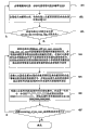
The flow process that reference frame is handled in the processing unit realization image of the embodiment of the invention comprises the steps: as shown in Figure 4
Step 401: before every frame decoding, initialization reference frame lists memory cell 305.Reference frame lists memory cell 305 is to be made of 16 reference frame registers and register read writing controller 309, and frame_R0 is to frame_R15, and each reference frame register bit wide is 16bit, and its value is the reference frame sequence number, in order to identify different reference frames.
Initialization procedure is as follows: when reference frame lists memory cell 305 receives that the initialization enable signal from control circuit 301 is that effectively (value of this enable signal can preestablish, for example set 1 for effective, 0 is invalid), register read writing controller 309 in the reference frame lists memory cell 305 reads the initial reference frame tabulation of initial reference frame list information input interface 307, and described initial reference frame tabulation is write 16 reference frame registers respectively.
Step 402: before every frame begins decoding, 302 two registers of initialization insertion position register 303 and address pointer register.Register 303 bit wides in insertion position are 16bit, and each of initial value is 1, i.e. 16 ' b1111,1111,1111,1111.The bit wide of address pointer register 302 is 16bit, and each is 0 initial value, i.e. 16 ' b0000,0000,0000,0000.
Step 403: control circuit 301 judges that whether syntax elements ref_pic_list_reordering_flag_l0 is 1, if then reorder, carry out step 404, otherwise goes to step 401.
Step 404: control circuit 301 calculates the reference frame sequence number that needs reorder according to the abs_diff_pic_num_minus1 or the long_term_pic_num of control interface 306 inputs, and the shift enable signal of address pointer register 302 put 1, begin to contrast the reference frame sequence number of a plurality of reference frame registers in the reference frame lists memory cell 305, equate with the reference frame sequence number that needs the rearrangement frame up to the reference frame sequence number of certain reference frame register of address pointer register 302 pointed.Detailed process is as follows:
After at control circuit 301 shift enable of address pointer register 302 being put first clock cycle of 1, address pointer register is by 16 ' b 0000,0000,0000,0000 becomes 16 ' b1000,0000,0000,0000, the address pointer of address pointer register 302 points to first register frame_R0 in the reference frame lists memory cell, and therefore, the reference frame sequence number of depositing among reference frame lists memory cell 305 first reference frame register of output frame_R0 is to comparator 304, comparator 304 with the need rearrangement reference frame sequence number of itself and control circuit 301 outputs relatively, if equate, comparator 304 sends to control circuit 301 and equates marking signal, and then control circuit 301 shift enable signal that will output to address pointer register 302 is changed to 0, address pointer register 302 stops displacement, forwards step 405 to.Otherwise, 302 each clock cycle of address pointer register move to right one successively, by 16 ' b 1000,0000,0000,0000 becomes 16 ' b 1100,0000,0000,0000, promptly address pointer points to second register, and the output of reference frame lists then respective change is the reference frame sequence number of depositing among the frame_R1, and compare once more, as equate to stop displacement, and unequally then once more address pointer register 302 being moved to right, the reference frame sequence number of depositing in address pointer register 302 reference frame register pointed equates with the reference frame sequence number that need reorder, control circuit 301 puts 0 with the shift enable of address pointer register 302, and forwards step 405 to.
Step 405: the content of the needs of being determined by positional information in the reference frame lists memory cell 305 being upgraded first register in the register replaces with the reference frame sequence number that need reorder, and the content of other registers of the needs that positional information is definite renewal is done the order displacement.Detailed process is as follows:
With the content input of depositing in insertion position register 303 and the address pointer register 302 put in place with logical calculated device 308 in do position and operation, obtain the location information signal of a 16bit bit wide, location information signal is represented the positional information of the reference frame register that needs upgrade.On behalf of frame_R0, the highest order of positional information need be updated for " 1 ", and to keep initial value constant for " 0 " is represented; On behalf of frame_R15, lowest order need be updated for " 1 ", and to keep initial value constant for " 0 " is represented.Whether other on behalf of corresponding registers, everybody need to be updated respectively.Register value such as insertion position register 303 is 16 ' b1111,1111,1111,1111, the register value of address pointer register 302 is 16 ' b1111,1111,0000,0000, address pointer register 302 currencys represent that the reference frame number of the 8th register in the current reference frame lists memory cell 305 equates with the frame number of the frame that need reorder.Step-by-step and the result be that the value of position information is 16 ' b1111,1111,0000,0000, expression frame_R0 need be updated to the value of 8 reference frame registers between the frame_R7.309 couples of frame_R0 of register read writing controller control upgrade operation to the value of 8 reference frame registers between the frame_R7, the register value of reference frame register frame_R0 is replaced by the frame number that need reorder, the register value of reference frame register frame_R1 is replaced by original reference frame sequence number of frame_R0, the register value of reference frame register frame_R2 is replaced by original reference frame sequence number of frame_R1, the rest may be inferred, and reference frame register frame_R (n) replaces the reference frame number of reference frame register frame_R (n-1) reference frame number of itself storing.Wherein, the n value is a natural number, the sum of 1≤n≤M reference frame register.
Below in conjunction with Fig. 5 the selection and the renewal process of the update content of above-mentioned reference frame register are described:
Comprise selector and determining device in the register read writing controller 309, selector is according to the register value from insertion position register 303, select reference frame register frame_R (n) lastest imformation reference frame sequence number that reorders from need and the register value of reference frame register frame_R (n-1), and described lastest imformation is sent to reference frame register frame_R (n); Determining device be used for judging whether to upgrade enable signal be 1 and positional information be 1 with the corresponding bit of reference frame register frame_R (n), write enable signal if then send to reference frame register frame_R (n):
(1) update content of frame_R0 only may be the reference frame sequence number that needs ordering, therefore need not to select according to the register value of insertion position register 303.If the 16th of positional information is 1, and renewal enables then the register value of reference frame register frame_R0 to be updated to the reference frame sequence number of need ordering into effectively.(2) frame_R1 when the 15th of positional information is 1 and renewal enable to effectively upgrading, update content is then selected according to the 16th of insertion position register 303, if the 16th of insertion position register 303 is 0, then select to reorder frame number, otherwise original reference frame sequence number of selection frame_R0 is as update content as update content.(3) frame_R2 is 1 and upgrades and enable to upgrade for effectively the time as the 14th of insertion position register 303, update content is used the 15th of register value of insertion position register 303 condition alternatively, if the 15th of the register value of insertion position register 303 is 0, then select to reorder frame number as update content, otherwise, select frame_r1 as update content.By that analogy, reference frame register frame_r (n) is with the 17-n position of insertion position register 303 register values (if the bit wide of insertion position register 303 is M, then the being the M-n+1 position) alternative condition as update content.
Specifically then as, register 303 values in insertion position are 16 ' b 0111,1111,1111,1111, the value of address pointer register 302 is 16 ' b 1111,1111,1100,0000, the reference frame number of the 10th reference frame register frame_R9 of the current reference frame lists memory cell 305 of the value representation of address pointer register 302 equates with the frame number of the frame that need reorder, step-by-step and the result be that the position information signal is 16 ' b0111,1111,1100,0000, expression reference frame register frame_R1 need be replaced to the value of 9 registers between the reference frame register frame_R9.The 15th according to the register value of insertion position register 303 is 0, reference frame register frame_R1 replaces current memory contents with the reorder frame number of frame of need, and reference frame register frame_R2 uses the value of previous register to substitute current self storing value to reference frame register frame_R9 successively.
Step 406: insertion position register 303 is carried out the right shift operation, and mend ' 0 ' at first.As 16 ' b1111,1111,1111,1111 right shifts are for becoming 16 ' b0111,1111,1111,1111.Address pointer register 302 is reset to 16 ' b 0000,0000,0000,0000.
Step 407: control circuit 301 judges whether the value of reordering_of_pic_num_idc equals 3, if then finish sequencer procedure, otherwise, going to step 404, repeated execution of steps 404 is to step 406.
The invention discloses the processing unit of reference frame in a kind of image, and use this processing unit to realize reference frame is handled in the image method and decoder.The present invention program is with respect to prior art, and speed has very big lifting, is applicable to the needs of HD video technical development more.
Satisfying under the prerequisite that does not change the present invention's design; part or all of employing equivalent electric circuit well known in the art or device that the embodiment of the invention proposes in the processing unit are replaced, and obtain various be used for device that reference frame reorders all should be in protection scope of the present invention.For example address pointer register 302 wherein or insertion position register 303 can be realized same function with adder.
The above only is preferred embodiment of the present invention, not in order to restriction the present invention, all any modifications of being done within the spirit and principles in the present invention, is equal to and replaces and improvement etc., all should be included within protection scope of the present invention.