CN101546067B - Image display apparatus and optical compensation device - Google Patents
Image display apparatus and optical compensation device Download PDFInfo
- Publication number
- CN101546067B CN101546067B CN2009101291215A CN200910129121A CN101546067B CN 101546067 B CN101546067 B CN 101546067B CN 2009101291215 A CN2009101291215 A CN 2009101291215A CN 200910129121 A CN200910129121 A CN 200910129121A CN 101546067 B CN101546067 B CN 101546067B
- Authority
- CN
- China
- Prior art keywords
- optical compensation
- compensation plate
- liquid crystal
- plate
- optical
- Prior art date
- Legal status (The legal status is an assumption and is not a legal conclusion. Google has not performed a legal analysis and makes no representation as to the accuracy of the status listed.)
- Expired - Fee Related
Links
Images


Classifications
-
- G—PHYSICS
- G02—OPTICS
- G02F—OPTICAL DEVICES OR ARRANGEMENTS FOR THE CONTROL OF LIGHT BY MODIFICATION OF THE OPTICAL PROPERTIES OF THE MEDIA OF THE ELEMENTS INVOLVED THEREIN; NON-LINEAR OPTICS; FREQUENCY-CHANGING OF LIGHT; OPTICAL LOGIC ELEMENTS; OPTICAL ANALOGUE/DIGITAL CONVERTERS
- G02F1/00—Devices or arrangements for the control of the intensity, colour, phase, polarisation or direction of light arriving from an independent light source, e.g. switching, gating or modulating; Non-linear optics
- G02F1/01—Devices or arrangements for the control of the intensity, colour, phase, polarisation or direction of light arriving from an independent light source, e.g. switching, gating or modulating; Non-linear optics for the control of the intensity, phase, polarisation or colour
- G02F1/13—Devices or arrangements for the control of the intensity, colour, phase, polarisation or direction of light arriving from an independent light source, e.g. switching, gating or modulating; Non-linear optics for the control of the intensity, phase, polarisation or colour based on liquid crystals, e.g. single liquid crystal display cells
- G02F1/133—Constructional arrangements; Operation of liquid crystal cells; Circuit arrangements
- G02F1/1333—Constructional arrangements; Manufacturing methods
- G02F1/1335—Structural association of cells with optical devices, e.g. polarisers or reflectors
- G02F1/13363—Birefringent elements, e.g. for optical compensation
- G02F1/133634—Birefringent elements, e.g. for optical compensation the refractive index Nz perpendicular to the element surface being different from in-plane refractive indices Nx and Ny, e.g. biaxial or with normal optical axis
-
- G—PHYSICS
- G02—OPTICS
- G02F—OPTICAL DEVICES OR ARRANGEMENTS FOR THE CONTROL OF LIGHT BY MODIFICATION OF THE OPTICAL PROPERTIES OF THE MEDIA OF THE ELEMENTS INVOLVED THEREIN; NON-LINEAR OPTICS; FREQUENCY-CHANGING OF LIGHT; OPTICAL LOGIC ELEMENTS; OPTICAL ANALOGUE/DIGITAL CONVERTERS
- G02F2201/00—Constructional arrangements not provided for in groups G02F1/00 - G02F7/00
- G02F2201/38—Anti-reflection arrangements
-
- G—PHYSICS
- G02—OPTICS
- G02F—OPTICAL DEVICES OR ARRANGEMENTS FOR THE CONTROL OF LIGHT BY MODIFICATION OF THE OPTICAL PROPERTIES OF THE MEDIA OF THE ELEMENTS INVOLVED THEREIN; NON-LINEAR OPTICS; FREQUENCY-CHANGING OF LIGHT; OPTICAL LOGIC ELEMENTS; OPTICAL ANALOGUE/DIGITAL CONVERTERS
- G02F2413/00—Indexing scheme related to G02F1/13363, i.e. to birefringent elements, e.g. for optical compensation, characterised by the number, position, orientation or value of the compensation plates
- G02F2413/02—Number of plates being 2
-
- G—PHYSICS
- G02—OPTICS
- G02F—OPTICAL DEVICES OR ARRANGEMENTS FOR THE CONTROL OF LIGHT BY MODIFICATION OF THE OPTICAL PROPERTIES OF THE MEDIA OF THE ELEMENTS INVOLVED THEREIN; NON-LINEAR OPTICS; FREQUENCY-CHANGING OF LIGHT; OPTICAL LOGIC ELEMENTS; OPTICAL ANALOGUE/DIGITAL CONVERTERS
- G02F2413/00—Indexing scheme related to G02F1/13363, i.e. to birefringent elements, e.g. for optical compensation, characterised by the number, position, orientation or value of the compensation plates
- G02F2413/10—Indexing scheme related to G02F1/13363, i.e. to birefringent elements, e.g. for optical compensation, characterised by the number, position, orientation or value of the compensation plates with refractive index ellipsoid inclined, or tilted, relative to the LC-layer surface O plate
Landscapes
- Physics & Mathematics (AREA)
- Nonlinear Science (AREA)
- Mathematical Physics (AREA)
- Chemical & Material Sciences (AREA)
- Crystallography & Structural Chemistry (AREA)
- General Physics & Mathematics (AREA)
- Optics & Photonics (AREA)
- Liquid Crystal (AREA)
- Polarising Elements (AREA)
Abstract
一种图像显示装置以及光学补偿设备,所述图像显示装置包括:液晶板,具有被放置于一对基板之间的液晶层;以及光学补偿板对,包括第一光学补偿板和第二光学补偿板,所述第一光学补偿板由负单轴晶体形成以及所述第二光学补偿板由正单轴晶体形成。光学补偿对被配置成使得所述第一光学补偿板与所述第二光学补偿板之间厚度的差所引起的光相位差把液晶板所生成的光相位差抵消。
An image display device and an optical compensation device, the image display device including: a liquid crystal panel having a liquid crystal layer placed between a pair of substrates; and a pair of optical compensation plates including a first optical compensation plate and a second optical compensation plate plates, the first optical compensation plate is formed of a negative uniaxial crystal and the second optical compensation plate is formed of a positive uniaxial crystal. The optical compensation pair is configured such that the optical phase difference caused by the thickness difference between the first optical compensation plate and the second optical compensation plate cancels the optical phase difference generated by the liquid crystal panel.
Description
相关申请的交叉引用Cross References to Related Applications
本发明包含2008年3月25日提交日本专利局的日本专利申请JP2008-077401所涉及的主题,该申请的全部内容经引用并入本文。The present invention contains subject matter related to Japanese Patent Application JP2008-077401 filed in the Japan Patent Office on Mar. 25, 2008, the entire content of which is hereby incorporated by reference.
技术领域technical field
本发明涉及具有液晶板的图像显示装置以及与所述液晶板一同使用的光学补偿设备。The present invention relates to an image display device having a liquid crystal panel and an optical compensation device for use with the liquid crystal panel.
背景技术Background technique
已经存在具有液晶板的图像显示装置的实例。图像显示装置的实例包括液晶投影机装置,其中液晶板被用作光调制器。液晶投影机装置被配置成把用液晶板调制的图像投影到屏幕上,并被广泛地用作用于对会议或演讲的演示材料进行放大和投影的器件。There have been examples of image display devices having liquid crystal panels. Examples of image display devices include liquid crystal projector devices in which a liquid crystal panel is used as a light modulator. A liquid crystal projector device is configured to project an image modulated with a liquid crystal panel onto a screen, and is widely used as a device for magnifying and projecting presentation materials for meetings or lectures.
对于液晶投影机装置,需要对投影图像的图像质量进行改进。定义投影图像的质量的重要因素之一是对比度。对比度是黑色显示状态与白色显示状态之间亮度的比。For liquid crystal projector devices, there is a need to improve the image quality of projected images. One of the important factors that define the quality of a projected image is contrast. The contrast ratio is a ratio of brightness between a black display state and a white display state.
在液晶投影机装置中,尽可能地使黑色显示的亮度最小化以改进对比度是有效的。然而在实际中,某些因素,例如被用作光调制器的液晶板的结构或性质、以及从照明系统进入液晶板的光的状态,会使得即使是在黑色显示状态也会引起漏光。In a liquid crystal projector device, it is effective to minimize the brightness of black display as much as possible to improve the contrast. In practice, however, certain factors, such as the structure or properties of a liquid crystal panel used as a light modulator, and the state of light entering the liquid crystal panel from an illumination system, cause light leakage even in a black display state.
为了防止这种漏光,提出了用于液晶板的光学补偿的技术。例如,使用多层薄膜(例如,见日本专利No.3162210),或者使用双折射板(例如,见日本专利No.3864929)。可替选地,使用复数个包括正单轴双折射材料的双折射元件(例如,见日本未经审查的专利申请公开No.2007-286609)。In order to prevent such light leakage, a technique for optical compensation of liquid crystal panels has been proposed. For example, a multilayer film is used (for example, see Japanese Patent No. 3162210), or a birefringent plate is used (for example, see Japanese Patent No. 3864929). Alternatively, a plurality of birefringent elements including a positive uniaxial birefringent material are used (for example, see Japanese Unexamined Patent Application Publication No. 2007-286609).
发明内容Contents of the invention
近来,提倡把垂直取向(VA)液晶,而不是以前广泛使用的扭曲向列(TN)液晶,用于液晶投影机装置的液晶板。VA液晶是如下类型的液晶:在不施加电压时垂直于基板排列,在施加电压时相对于基板的法线倾斜。VA液晶展现了高速以及高对比度的特性。Recently, vertical alignment (VA) liquid crystals have been advocated for use in liquid crystal panels of liquid crystal projector devices, instead of twisted nematic (TN) liquid crystals that have been widely used previously. The VA liquid crystal is a type of liquid crystal that is aligned vertically to the substrate when no voltage is applied, and is inclined with respect to the normal to the substrate when a voltage is applied. VA liquid crystal exhibits high-speed and high-contrast characteristics.
在VA液晶中,液晶在不施加电压时垂直于基板排列,被称为“常黑”,对于垂直于面板表面的入射光不会出现相位差。然而在实际中,由于一些原因,液晶以大约几度的预倾角来排列,而不是完全垂直地排列。这对于垂直于面板表面的入射光也会引起相位差,导致漏光。来自照明系统的进来的光也垂直于面板表面进入并按照对应于光的F值的发散角分布进行入射。这也会引起相位差,导致漏光。换言之,即使是使用VA液晶,在黑色显示状态中也会出现漏光。In VA liquid crystal, the liquid crystal is aligned perpendicular to the substrate when no voltage is applied, which is called "normally black", and no phase difference occurs for incident light perpendicular to the panel surface. In practice, however, the liquid crystals are aligned with a pretilt angle of about several degrees instead of being perfectly vertically aligned due to some reasons. This also causes a phase difference for incident light perpendicular to the panel surface, resulting in light leakage. Incoming light from the lighting system also enters perpendicular to the panel surface and is incident with a divergence angle distribution corresponding to the F-number of the light. This also causes a phase difference, resulting in light leakage. In other words, even when VA liquid crystals are used, light leakage occurs in a black display state.
在仿真中,其中的液晶以预倾角排列、有一定厚度的VA液晶可以被建模成倾斜的正型C板。被用于VA液晶的光学补偿以防止漏光的可能的机制是,把被用作负型C板的光学补偿板按与该VA液晶的预倾角同样的方向进行倾斜来排列,以抵消光相位差。In the simulation, the VA liquid crystals in which the liquid crystals are arranged at a pre-tilt angle and have a certain thickness can be modeled as a tilted positive C-plate. The possible mechanism used for optical compensation of VA liquid crystals to prevent light leakage is to arrange the optical compensation plate used as a negative C plate by tilting in the same direction as the pretilt angle of the VA liquid crystal to cancel the optical retardation .
如日本专利No.3162210中所公开的,薄膜是多层的且明显是作为负型C板来执行补偿。在此技术中,垂直于薄膜表面的方向是负方向。当此技术被应用于VA液晶时,必须要在形成薄膜后把薄膜设置成按预倾角进行倾斜。在此技术中,是假定使用TN液晶。因此,难以把该技术应用于VA液晶,因为难以减小装置的尺寸(或减小用于所述装置的空间)。此外,根据安装位置,还会出现象散。As disclosed in Japanese Patent No. 3162210, the thin film is multilayered and apparently performs compensation as a negative C-plate. In this technique, the direction perpendicular to the surface of the film is the negative direction. When this technique is applied to VA liquid crystals, it is necessary to set the film to be inclined at a pre-tilt angle after forming the film. In this technique, it is assumed that TN liquid crystals are used. Therefore, it is difficult to apply this technology to VA liquid crystals because it is difficult to reduce the size of the device (or reduce the space for the device). In addition, depending on the installation location, astigmatism may also occur.
上述日本专利No.3864929所公开的技术中,也是假定使用TN液晶。因此,当该技术被应用于VA液晶时,如果按各自的特性使得能够按把液晶相位差抵消的方向来排列双折射元件,则双折射板薄得约几十微米(μm)。因此,形成、加工以及处理这种双折射板会是困难的。In the technique disclosed in the aforementioned Japanese Patent No. 3864929, the use of TN liquid crystals is also assumed. Therefore, when this technique is applied to VA liquid crystals, if the birefringent elements are arranged in a direction that cancels the phase difference of liquid crystals according to their respective characteristics, the birefringent plates are as thin as about several tens of micrometers (μm). Therefore, forming, processing, and handling such a birefringent plate can be difficult.
上述日本未经审查的专利申请公开No.2007-286609所公开的技术中,是假定使用VA液晶。然而,必须要使用复数个包括正单轴晶体、被形成和加工成厚度约几十微米(μm)的光学补偿板。形成和加工是困难的且从成本而言没有优势。In the technique disclosed in the aforementioned Japanese Unexamined Patent Application Publication No. 2007-286609, it is assumed that VA liquid crystals are used. However, it is necessary to use a plurality of optical compensation plates including positive uniaxial crystals, formed and processed to a thickness of about several tens of micrometers (μm). Forming and processing is difficult and not advantageous in terms of cost.
从而,在相关领域的技术中,对于液晶板的光学补偿无法必然获得紧凑的装置配置以及容易的批量生产(低成本实施)。Thus, in the technology of the related art, compact device configuration and easy mass production (low-cost implementation) cannot necessarily be obtained for optical compensation of a liquid crystal panel.
从而,期望的是:通过在确保紧凑的装置配置以及容易的批量生产的情况下使用液晶板的光学补偿,提供一种获得增加的对比度的图像显示装置和光学补偿设备以提供期望的图像质量,而不论液晶板是TN液晶板还是VA液晶板。Thus, it is desirable to provide an image display device and an optical compensation device that obtain an increased contrast ratio to provide desired image quality by using optical compensation of a liquid crystal panel while ensuring a compact device configuration and easy mass production, Regardless of whether the LCD panel is a TN LCD panel or a VA LCD panel.
根据本发明的实施例,图像显示装置包括:液晶板,具有被放置于一对基板之间的液晶层;以及光学补偿板对,包括第一光学补偿板和第二光学补偿板,所述第一光学补偿板由负单轴晶体形成以及所述第二光学补偿板由正单轴晶体形成,其中,所述第一光学补偿板与所述第二光学补偿板之间厚度的差所引起的光相位差把液晶板所生成的光相位差抵消。According to an embodiment of the present invention, an image display device includes: a liquid crystal panel having a liquid crystal layer disposed between a pair of substrates; and a pair of optical compensation plates including a first optical compensation plate and a second optical compensation plate, the first optical compensation plate An optical compensation plate is formed of a negative uniaxial crystal and the second optical compensation plate is formed of a positive uniaxial crystal, wherein a difference in thickness between the first optical compensation plate and the second optical compensation plate is caused by The optical phase difference cancels the optical phase difference generated by the liquid crystal panel.
在具有上述配置的图像显示装置中,由负单轴晶体形成并被用作负型C板的第一光学补偿板与由正单轴晶体形成并被用作正型C板的第二光学补偿板的组合提供液晶板的光学补偿。换言之,液晶板所生成的光相位差被第一光学补偿板与第二光学补偿板之间厚度的差所引起的光相位差抵消。例如,当液晶板被建模成正型C板时,在实践中,仅通过使用第一光学补偿板难以对其进行补偿,因为第一光学补偿板太薄。然而,由于利用了第一光学补偿板与第二光学补偿板之间厚度的差所引起的光相位差,执行液晶板的光学补偿是可能的,且保证了第一光学补偿板和第二光学补偿板实践上可接受的厚度。此外,第一光学补偿板和第二光学补偿板中的每个都是由单轴晶体形成。因此,这些板被形成为使得晶体的光轴倾斜,这就能够支持液晶板中液晶排列的预倾角而无需使这些板倾斜。In the image display device having the above-described configuration, the first optical compensation plate formed of a negative uniaxial crystal and used as a negative C plate and the second optical compensation plate formed of a positive uniaxial crystal and used as a positive C plate The combination of panels provides optical compensation for the liquid crystal panel. In other words, the optical phase difference generated by the liquid crystal panel is offset by the optical phase difference caused by the thickness difference between the first optical compensation plate and the second optical compensation plate. For example, when the liquid crystal panel is modeled as a positive C-plate, in practice, it is difficult to compensate for it only by using the first optical compensation plate because the first optical compensation plate is too thin. However, since the optical phase difference caused by the difference in thickness between the first optical compensation plate and the second optical compensation plate is utilized, it is possible to perform optical compensation of the liquid crystal panel, and it is ensured that the first optical compensation plate and the second optical compensation plate The practically acceptable thickness of the compensation plate. In addition, each of the first optical compensation plate and the second optical compensation plate is formed of a uniaxial crystal. Therefore, the plates are formed such that the optical axes of the crystals are tilted, which can support the pretilt angle of liquid crystal alignment in the liquid crystal panel without tilting the plates.
根据本发明的实施例,从而,通过把由负单轴晶体形成的第一光学补偿板与由正单轴晶体形成的第二光学补偿板进行组合所构建的光学补偿板对被用来执行液晶板的光学补偿。从而,不论液晶板是TN液晶板还是VA液晶板,通过使用液晶板的光学补偿都可以获得增加的对比度,以提供期望的图像质量。此外,即使在此情形中,也可以保证第一光学补偿板和第二光学补偿板实践上可接受的厚度。再者,不必倾斜第一光学补偿板和第二光学补偿板来支持液晶排列的预倾角。从而可以获得紧凑的装置配置以及容易的批量生产。According to an embodiment of the present invention, thus, a pair of optical compensation plates constructed by combining a first optical compensation plate formed of a negative uniaxial crystal with a second optical compensation plate formed of a positive uniaxial crystal is used to implement liquid crystal Plate optical compensation. Thus, regardless of whether the liquid crystal panel is a TN liquid crystal panel or a VA liquid crystal panel, increased contrast can be obtained by using optical compensation of the liquid crystal panel to provide desired image quality. Furthermore, even in this case, practically acceptable thicknesses of the first optical compensation plate and the second optical compensation plate can be secured. Furthermore, it is not necessary to tilt the first optical compensation plate and the second optical compensation plate to support the pre-tilt angle of liquid crystal alignment. Thereby, a compact device configuration and easy mass production can be obtained.
附图说明Description of drawings
图1是示意性地示出了三板液晶投影机装置的实例结构的示意图;1 is a schematic diagram schematically showing an example structure of a three-plate liquid crystal projector device;
图2是示出了根据本发明实施例的液晶投影机装置的主要部分的实例结构的示意图;2 is a schematic diagram showing an example structure of a main part of a liquid crystal projector device according to an embodiment of the present invention;
图3是示意性地示出了根据本发明实施例的光学补偿设备的有益效果的图;3 is a diagram schematically illustrating the beneficial effects of an optical compensation device according to an embodiment of the present invention;
图4是示出了光学补偿的第一具体示例性模型的图;FIG. 4 is a diagram illustrating a first specific exemplary model of optical compensation;
图5是示出了光学补偿的第二具体示例性模型的图;FIG. 5 is a diagram illustrating a second specific exemplary model of optical compensation;
图6是示出了光学补偿的第三具体示例性模型的图;FIG. 6 is a diagram illustrating a third specific exemplary model of optical compensation;
图7是示出了光学补偿的第四具体示例性模型的图;FIG. 7 is a diagram illustrating a fourth specific exemplary model of optical compensation;
图8是示出了用于形成光学补偿板的具体方法的实例的图;FIG. 8 is a diagram showing an example of a specific method for forming an optical compensation plate;
图9A和9B是示出了通过图8所示的流程所产生的光学补偿板的实例结构的图;9A and 9B are diagrams showing an example structure of an optical compensation plate produced by the flow shown in FIG. 8;
图10A和10B是示出了光学系统的视角特性的仿真结果的具体实例的图;10A and 10B are graphs showing specific examples of simulation results of viewing angle characteristics of an optical system;
图11是示出了根据本发明实施例的液晶投影机装置的主要部分的另一实例结构的示意图;FIG. 11 is a schematic diagram showing another example structure of a main part of a liquid crystal projector device according to an embodiment of the present invention;
图12是示意性地示出了三板液晶投影机装置的另一实例结构的示意图;以及FIG. 12 is a schematic diagram schematically showing another example structure of a three-plate liquid crystal projector device; and
图13是示出了根据本发明实施例的液晶投影机装置的主要部分的又一实例结构以及示出了图12所示的液晶投影机装置的主要部分的实例结构的示意图。13 is a schematic diagram showing still another example structure of a main part of a liquid crystal projector device according to an embodiment of the present invention and showing an example structure of a main part of the liquid crystal projector device shown in FIG. 12 .
具体实施方式Detailed ways
现在将参考附图对根据本发明实施例的图像显示装置和光学补偿设备进行描述。An image display device and an optical compensation device according to an embodiment of the present invention will now be described with reference to the accompanying drawings.
首先,将给出液晶投影机装置的示意性结构的描述,所述液晶投影机装置是根据本发明实施例的图像显示装置的具体实例。包括分别对应于红色(R)、绿色(G)和蓝色(B)的液晶板的液晶投影机装置(称为三板液晶投影机装置)是广泛存在的。First, a description will be given of a schematic structure of a liquid crystal projector device which is a specific example of an image display device according to an embodiment of the present invention. Liquid crystal projector devices including liquid crystal panels respectively corresponding to red (R), green (G), and blue (B) (referred to as three-panel liquid crystal projector devices) are widely available.
图1是示意性地示出了三板液晶投影机装置的实例结构的示意图。FIG. 1 is a diagram schematically showing an example structure of a three-panel liquid crystal projector device.
如图1所示的实例所示,在液晶投影机装置中,从光源1出射的光通过被配置成用来阻隔红外辐射或紫外辐射的滤光器2、复眼透镜3、以及被配置成用来把非偏振波转换成偏振波的PS分离器/合成器4,并随后被引导至被配置成仅对特定波段的光进行反射的二向色镜5。二向色镜5把光分成R、G和B的彩色光分量。彩色光分量通过被配置成用来吸收紫外辐射的滤光器6,按照需要,通过全反射镜7、聚光透镜8、替续透镜9、以及其它任何恰当的合适的元件,并分别入射到为R、G和B色提供的液晶板10R、10G和10B上。根据液晶板10R、10G和10B中的视频信号对彩色光分量进行调制之后,进行了光调制的彩色光分量通过1/2波长的膜21被引导至二向色棱镜22,如果必要的话,并且被进行组合,然后使用投影机镜头23进行放大和投影。在液晶投影机装置中,相应地在屏幕上显示彩色图像。As shown in the example shown in FIG. 1 , in a liquid crystal projector device, light emitted from a light source 1 passes through a
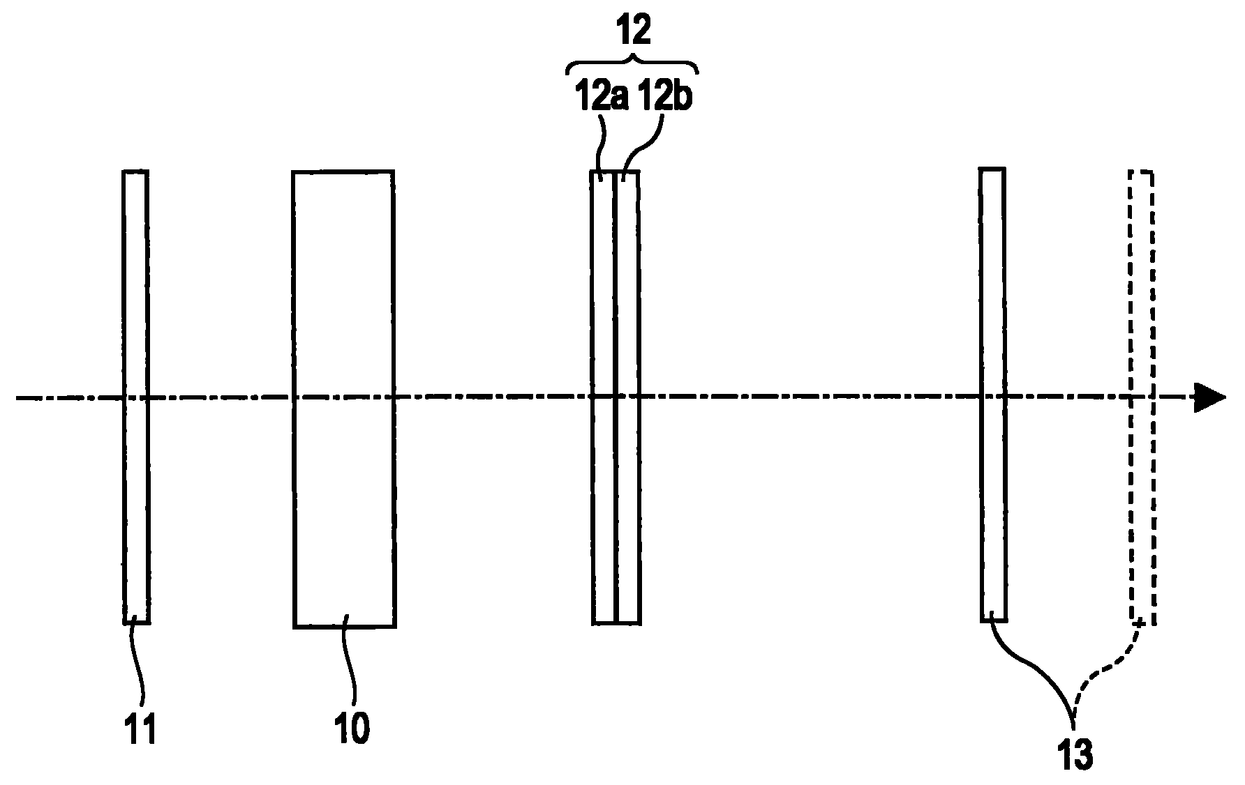
为液晶板10R、10G和10B中的每个液晶板都提供有入射侧偏振板11、光学补偿板对12、以及出射侧偏振板13。透射通过入射侧偏振板11的各彩色光分量入射到液晶板10R、10G和10B上,以及,在液晶板10R、10G和10B中进行了光调制的彩色光分量透射通过光学补偿板对12和出射侧偏振板13。An incident-side
现在将对液晶投影机装置中的主要部分的结构进行描述。The structure of the main parts in the liquid crystal projector device will now be described.
图2是示出了液晶投影机装置的主要部分的实例结构的示意图。在图2所示的实例中,包括入射侧偏振板11、液晶板10R、10G和10B、光学补偿板对12、以及出射侧偏振板13的部分中的每个都以放大的尺寸示出。FIG. 2 is a schematic diagram showing an example structure of a main part of a liquid crystal projector device. In the example shown in FIG. 2 , each of portions including the incident-side
如图2所示的实例所示,在RGB彩色光分量中每个彩色光分量的光路上,被用作光调制器的液晶板10R、10G和10B(以下简称为“液晶板10”)中相应的一个以及光学补偿板对12被排列在具有正交尼科尔排列(即,偏振方向彼此垂直)的入射侧偏振板11与出射侧偏振板13之间,所以光学补偿板对12可以位于光出射侧。可以提供复数个出射侧偏振板13。入射侧偏振板11和出射侧偏振板13可以是有机偏振板也可以是无机偏振板。与有机偏振板相比,无机偏振板即使是在被用在其中来自光源1的光的量很大的液晶投影机装置中时也能够减少性能恶化,并提供更长的寿命和更高的可靠性。As shown in the example shown in FIG. 2, on the optical path of each of the RGB color light components,
液晶板10具有被放置于一对基板之间的液晶层。液晶层中液晶的排列根据施加到其上的电压而变化,以使得液晶板10能够起用于透射的光的光调制器的作用。The
液晶板10可以是由VA液晶制成的。VA液晶被设计成以垂直取向模式进行工作。在不施加电压时,液晶垂直于基板排列,且所述液晶在施加电压时相对于基板的法线倾斜。然而在实际中,即使是在不施加电压时,液晶也是以约几度的预倾角来进行排列,而不是完全垂直于基板。即,液晶板10被配置成使得液晶分子在不施加电压的情况下以预定的预倾角倾斜。The
如本领域中所公知的,包括VA液晶的液晶板被用作正型C板。正型C板是指具有各向同性的平面内折射率并在其厚度方向具有大的折射率的介质。As is well known in the art, a liquid crystal panel including VA liquid crystals is used as a positive type C plate. A positive C-plate refers to a medium having an isotropic in-plane refractive index and a large refractive index in its thickness direction.
光学补偿板对12被设计成提供液晶板10的光学补偿以防止所述液晶板10的黑色显示状态中的漏光。The optical
光学补偿板对12包括包含负单轴晶体的第一光学补偿板12a以及包含正单轴晶体的第二光学补偿板12b。光学补偿板对12被配置成使得第一光学补偿板12a与第二光学补偿板12b之间厚度的差所引起的光相位差把液晶板10所生成的光相位差抵消。The pair of
负单轴晶体是具有负的单轴光学各向异性的晶体,其具体的实例是蓝宝石。由这种负单轴晶体所形成的第一光学补偿板12a被用作负型C板。负型C板是指具有各向同性的平面内折射率并在其厚度方向具有小的折射率的介质。A negative uniaxial crystal is a crystal having negative uniaxial optical anisotropy, a specific example of which is sapphire. The first
另一方面,正单轴晶体是具有正的单轴光学各向异性的晶体,其具体的实例是石英。由这种正单轴晶体所形成的第二光学补偿板12b被用作正型C板。On the other hand, a positive uniaxial crystal is a crystal having positive uniaxial optical anisotropy, a specific example of which is quartz. The second
即,光学补偿板对12是通过把包含负单轴晶体并被用作负型C板的第一光学补偿板与包含正单轴晶体并被用作正型C板的第二光学补偿板进行组合来构建的。由于第一光学补偿板12a与第二光学补偿板12b之间厚度的差,光学补偿板对12整体上被用作负型C板。That is, the optical
可以把第一光学补偿板12a与第二光学补偿板12b成一整体地排列,以便可以使第一光学补偿板12a的光出射表面与第二光学补偿板12b的光入射表面相互接触。The first
此外,由于液晶板10的液晶层中的液晶分子以预定的预倾角倾斜,第一光学补偿板12a和第二光学补偿板12b可以被配置成使它们的光轴在与所述预倾角的倾斜方向相一致的方向中进行倾斜,以下将对此进行详细描述。In addition, since the liquid crystal molecules in the liquid crystal layer of the
现在将对具有上述结构的液晶投影机装置(特别是其主要部分,即光学补偿板对12)的效果进行描述。光学补偿板对12是根据本发明实施例的光学补偿设备的一种实施。Now, the effect of the liquid crystal projector device having the above structure (particularly its main part, ie, the pair of optical compensation plates 12) will be described. The optical
图3是示意性地示出了根据本发明实施例的光学补偿设备的有益效果的图。更具体地,图3是示意性地示出了液晶板10的折射率椭球的效果、第一光学补偿板12a的折射率椭球的效果以及第二光学补偿板12b的折射率椭球的效果的图。FIG. 3 is a diagram schematically illustrating the beneficial effect of an optical compensation device according to an embodiment of the present invention. More specifically, FIG. 3 schematically shows the effect of the refractive index ellipsoid of the
液晶板10是VA液晶板,其中液晶层以垂直取向模式进行工作,且可以被建模成正单轴晶体。换言之,在不施加电压的状态中以预倾角倾斜的VA液晶层是倾斜的正型C板。The
形成第一光学补偿板12a的蓝宝石板是由负单轴晶体制成的。即,蓝宝石板被用作负型C板,所述负型C板在光线通过它时引起与VA液晶的相位差符号相反的相位差。在使光轴倾斜来进行使用的时候,蓝宝石板被用作倾斜的负型C板。The sapphire plate forming the first
形成第二光学补偿板12b的石英板是由正单轴晶体制成的。在使光轴倾斜来进行使用的时候,石英板被用作倾斜的正型C板。The quartz plate forming the second
相应地,当液晶板10、第一光学补偿板12a、以及第二光学补偿板12b的光轴按基本上相同的方向进行倾斜时,作为正型C板的液晶板10和第二光学补偿板12b所生成的相位差符号相同,而作为负型C板的第一光学补偿板12a所生成的相位差符号相反。对液晶板10、第一光学补偿板12a、以及第二光学补偿板12b的厚度进行调整,以使得液晶板10和第二光学补偿板12b所生成的相位差的大小之和与第一光学补偿板12a所生成的相位差的大小相等,以防止处于正交尼科尔关系的入射侧偏振板11与出射侧偏振板13之间的相位移动。这使得液晶板10所生成的相位差能够被第一光学补偿板12a与第二光学补偿板12b之间厚度的差所生成的相位差抵消。Correspondingly, when the optical axes of the
在与液晶板10的预倾角基本上相同的方向上对第一光学补偿板12a和第二光学补偿板12b的厚度进行调整,可使得第一光学补偿板12a和第二光学补偿板12b由于它们之间厚度的差而被用作负型C板。结果是,抵消了液晶板10所生成的相位差。Adjusting the thicknesses of the first
为使得对此更容易理解,将用模型给出描述。To make this easier to understand, a description will be given using a model.
图4是示出了光学补偿的第一具体示例性模型的图。FIG. 4 is a diagram showing a first specific exemplary model of optical compensation.
在图4中,部分(a)示出了正单轴晶体的折射率椭球,其中,X轴和Y轴方向的寻常光线折射率no彼此相等,而Z轴(光轴)方向的非常光线折射率ne大于寻常光线折射率no(no<ne)。在图4中,部分(b)示出了负单轴晶体的折射率椭球,其中,X轴和Y轴方向的寻常光线折射率no彼此相等,而Z轴方向的非常光线折射率ne小于寻常光线折射率no(no>ne)。把图4的部分(a)和部分(b)所示的折射率椭球加在一起生成了图4的部分(c)所示的明显为各向同性的折射率椭球。在此情形中,对于来自任何方向的光,寻常光线折射率与非常光线折射率彼此相等(no=ne),不出现相位差。各相位差的量值由Δn(ne与no之间的差)×厚度来确定,其中,Δn由属性的值来定义。因此,可以通过对厚度进行调整来确定相位差的量值。In Fig. 4, part (a) shows the refractive index ellipsoid of a positive uniaxial crystal, in which the ordinary ray refractive index no in the X-axis and Y-axis directions is equal to each other, and the extraordinary ray in the Z-axis (optical axis) direction The refractive index ne is greater than the ordinary ray refractive index no (no<ne). In Fig. 4, part (b) shows the refractive index ellipsoid of the negative uniaxial crystal, in which the ordinary ray refractive index no in the X-axis and Y-axis directions is equal to each other, and the extraordinary ray refractive index ne in the Z-axis direction is less than Ordinary ray refractive index no (no>ne). Adding together the index ellipsoids shown in parts (a) and (b) of FIG. 4 yields the apparently isotropic index ellipsoid shown in part (c) of FIG. 4 . In this case, for light from any direction, the ordinary ray refractive index and the extraordinary ray refractive index are equal to each other (no=ne), and no phase difference occurs. The magnitude of each phase difference is determined by Δn (difference between ne and no)×thickness, where Δn is defined by the value of the attribute. Therefore, the magnitude of the phase difference can be determined by adjusting the thickness.
图5是示出了光学补偿的第二具体示例性模型的图。在图5所示的实例中,Z轴相对于图4所示模型的Z轴进行了倾斜。FIG. 5 is a diagram showing a second specific exemplary model of optical compensation. In the example shown in FIG. 5 , the Z axis is tilted relative to the Z axis of the model shown in FIG. 4 .
在图5中,部分(a)示出了Z轴以给定角度倾斜的情况下正单轴晶体的折射率椭球。这相当于在不施加电压的状态中以预倾角倾斜的VA液晶层。在图5中,部分(b)示出了Z轴以给定角度倾斜的情况下负单轴晶体的折射率椭球。这相当于被设置成使光轴倾斜的第一光学补偿板12a。所以,即使是在Z轴倾斜时,把图5的部分(a)和部分(b)所示的折射率椭球加在一起也生成了图5的部分(c)所示的明显为各向同性的折射率椭球。因此可以抵消各相位差。In FIG. 5 , part (a) shows the refractive index ellipsoid of a positive uniaxial crystal in the case where the Z axis is tilted at a given angle. This corresponds to a VA liquid crystal layer tilted at a pretilt angle in a state where no voltage is applied. In Fig. 5, part (b) shows the refractive index ellipsoid of the negative uniaxial crystal in the case where the Z axis is tilted at a given angle. This corresponds to the first
图6是示出了光学补偿的第三具体示例性模型的图。图6所示的实例示意了从图5的部分(b)的状态来切割被用作补偿板的平行板的概念,其中图5所示的模型中光轴倾斜。FIG. 6 is a diagram showing a third specific exemplary model of optical compensation. The example shown in FIG. 6 illustrates the concept of cutting a parallel plate used as a compensation plate from the state of part (b) of FIG. 5 in which the optical axis is inclined in the model shown in FIG. 5 .
如图6示出的实例所示,如果使光轴在被切割为平行板的补偿板的平面中进行倾斜,则在液晶投影机装置中安装所述补偿板时不必使它倾斜。从而,有益地,能够获得对液晶投影机装置的尺寸的减小(或对用于液晶投影机装置的空间的减小)。此外,不用担心象散。As shown in the example shown in FIG. 6, if the optical axis is inclined in the plane of the compensating plate cut as a parallel plate, it is not necessary to incline it when installing the compensating plate in a liquid crystal projector device. Thus, advantageously, a reduction in size of the liquid crystal projector device (or a reduction in space for the liquid crystal projector device) can be achieved. Also, don't worry about astigmatism.
然而,仅用作为负型C板的补偿板难以完成这一点,因为负单轴晶体所形成的补偿板的厚度是在几十微米(μm)的数量级。补偿板太薄而无法形成、加工以及处理这种补偿板。However, it is difficult to accomplish this with only a compensation plate used as a negative C-plate because the thickness of the compensation plate formed by negative uniaxial crystals is on the order of tens of micrometers (μm). The compensator is too thin to form, machine and handle such a compensator.
这是因为光学补偿板对12是通过把由负单轴晶体形成并被用作负型C板的第一光学补偿板12a与由正单轴晶体形成并被用作正型C板的第二光学补偿板12b进行组合来构建的。This is because the optical
图7是示出了光学补偿的第四具体示例性模型的图。FIG. 7 is a diagram showing a fourth specific exemplary model of optical compensation.
如在图5和图6中一样,在图7中,也是:部分(a)示出了VA液晶层被倾斜的情况下的折射率椭球,部分(b)示出了倾斜的负单轴晶体的折射率椭球。例如,假定由图7的部分(b)所示的负单轴晶体所形成的补偿板被设置在几百微米(μm)的数量级上,这不会在其生产中引起问题。在此情形中,把图7的部分(a)和部分(b)所示的折射椭球加在一起生成了如图7的部分(c)所示的明显为负型C板的折射率椭球,因为:图7的部分(b)所示的负单轴晶体所生成的相位差的量值大于图7的(a)所示的液晶层所生成的相位差的量值。为了获取各向同性折射率椭球,必须要额外提供正型C板的折射率椭球。这是因为光学补偿板对12是通过组合图7的部分(d)所示的正单轴晶体的折射率椭球来构建的。即,对由图7的部分(d)所示的正单轴晶体所形成的补偿板的厚度进行设置,以使得图7的部分(c)所示的相位差能够被抵消。从而,如图7的部分(e)所示,获取了明显为各向同性的折射率椭球。As in Fig. 5 and Fig. 6, in Fig. 7, too: part (a) shows the refractive index ellipsoid in the case where the VA liquid crystal layer is tilted, and part (b) shows the tilted negative uniaxial The refractive index ellipsoid of a crystal. For example, assuming that a compensation plate formed of a negative uniaxial crystal shown in part (b) of FIG. 7 is set on the order of several hundred micrometers (μm), this does not cause problems in its production. In this case, adding together the refraction ellipsoids shown in part (a) and part (b) of Fig. 7 produces the refraction ellipsoid which is clearly a negative C-plate as shown in part (c) of Fig. 7 ball, because: the magnitude of the phase difference generated by the negative uniaxial crystal shown in part (b) of FIG. 7 is larger than the magnitude of the phase difference generated by the liquid crystal layer shown in FIG. 7(a). In order to obtain an isotropic refractive index ellipsoid, the refractive index ellipsoid of the positive C plate must be additionally provided. This is because the optical
图8是示出了用于形成光学补偿板的具体方法的实例的图。FIG. 8 is a diagram showing an example of a specific method for forming an optical compensation plate.
在图8中,部分(a)示意性地示出了单轴晶体。单轴晶体的具体实例蓝宝石和石英在精确的理解(sense)中是三方晶系。在更广泛的理解中,蓝宝石和石英是六方晶系。在六方晶系系统中,c轴是光轴,以及还有晶体轴a1、a2和a3。为了使光学补偿板的光轴倾斜θ°,可以切割相对于与c轴垂直的平面(c平面)倾斜θ°的平行板。例如,如图8的部分(a)所示,如果把平行板切割成型为短边平行于a轴的矩形,如图8的部分(b)所示,则其长边平行于把m轴投影到该平行板的平面中所获得的m′轴。在此状态的平行板中,光轴(c轴)朝向m′轴倾斜θ°。如果把平行于m′轴的长边设置为参考平面,则液晶层的排列方向是相对于该参考平面倾斜45°的方向。为了使光轴在与液晶层的预倾角的方向同样的方向中进行倾斜,可以切割具有相对于平行板的参考平面进一步倾斜45°的参考平面的矩形板。最终所产生的板的朝向为图8的部分(c)所示的方式。从而,产生了在相对于参考平面倾斜45°的方向上具有倾斜θ°的光轴的光学补偿板。In Fig. 8, part (a) schematically shows a uniaxial crystal. Specific examples of uniaxial crystals sapphire and quartz are trigonal in a precise sense. In a broader understanding, sapphire and quartz are hexagonal. In the hexagonal system, the c-axis is the optical axis, and also the crystallographic axes a1, a2 and a3. In order to incline the optical axis of the optical compensation plate by θ°, a parallel plate inclined by θ° with respect to a plane (c-plane) perpendicular to the c-axis may be cut. For example, as shown in part (a) of Figure 8, if the parallel plate is cut into a rectangle whose short side is parallel to the a-axis, as shown in part (b) of Figure 8, its long side is parallel to the projection of the m-axis to the m' axis obtained in the plane of the parallel plate. In the parallel plate in this state, the optical axis (c axis) is inclined by θ° toward the m' axis. If the long side parallel to the m' axis is set as a reference plane, the alignment direction of the liquid crystal layer is a direction inclined by 45° with respect to the reference plane. In order to tilt the optical axis in the same direction as the direction of the pretilt angle of the liquid crystal layer, a rectangular plate with a reference plane further inclined by 45° relative to that of the parallel plate may be cut. The resulting panel was oriented in the manner shown in part (c) of FIG. 8 . Thus, an optical compensation plate having an optical axis inclined by θ° in a direction inclined by 45° relative to the reference plane was produced.
图9A和9B是示出了通过图8所示的流程所产生的光学补偿板的实例结构的图。图9A示出了液晶分子的预倾方向,图9B示出了光学补偿板的光轴方向。9A and 9B are diagrams showing an example structure of an optical compensation plate produced through the flow shown in FIG. 8 . FIG. 9A shows the pretilt direction of liquid crystal molecules, and FIG. 9B shows the direction of the optical axis of the optical compensation plate.
例如,如图9A所示,液晶板10的液晶层的预倾方向在相对于参考平面倾斜45°的方向上倾斜θ°。在此情形中,为了产生由第一光学补偿板12a与第二光学补偿板12b的组合所形成的光学补偿板对12,可以切割由负单轴晶体形成、形成第一光学补偿板12a的蓝宝石板以及由正单轴晶体形成、形成第二光学补偿板12b的石英板,以使得蓝宝石板和石英板的光轴的朝向沿着液晶分子的预倾角,并且这些板被加工成平行板。所切割的平行板被结合成如图9B所示的一体型的组件。可以按照具有约几百微米(μm)的厚度来形成平行板。借助于由第一光学补偿板12a与第二光学补偿板12b之间厚度的差所生成的光相位差来抵消液晶层所生成的光相位差的配置,如果它们中的一个的厚度增加,则其它的厚度也增加。获得了几百微米(μm)的厚度,这支持实践上的形成和加工以及实践上的处理。For example, as shown in FIG. 9A , the pretilt direction of the liquid crystal layer of the
注意,液晶板10的液晶层,由负单轴晶体形成、构成第一光学补偿板12a的蓝宝石板,以及由正单轴晶体形成、构成第二光学补偿板12b的石英板在折射率波长散射上是不同的。它们在Δn值(ne与no之间的差)上也是不同的,这是由材料决定的。考虑到这些情况,期望:包含蓝宝石的第一光学补偿板12a和包含石英的第二光学补偿板12b被设计成使得光轴的倾斜角度移动约几度(例如,约1°到5°,更优选地,约1°到3°),而不是完全等于液晶板10的液晶层的预倾角。Note that the liquid crystal layer of the
此外,优选地,包含蓝宝石的第一光学补偿板12a和包含石英的第二光学补偿板12b中的每个在与空气相接触的一侧都具有在其中所形成的抗反射(AR)涂层。AR涂层能够提高透射率。Furthermore, preferably, each of the first
进一步地,蓝宝石的折射率约为1.77,石英的折射率约为1.55。粘合它们的粘合剂的折射率约为1.5。由于石英与粘合剂之间折射率的差较小,在它们之间的边界上基本上不出现反射。另一方面,蓝宝石与粘合剂之间折射率的差较大,它们之间的边界上的反射会导致透射率降低。从而,优选地,在蓝宝石和粘合剂互相接触的表面上也形成AR涂层。Further, the refractive index of sapphire is about 1.77, and the refractive index of quartz is about 1.55. The adhesive that holds them together has a refractive index of about 1.5. Since the difference in refractive index between the quartz and the binder is small, substantially no reflection occurs at the boundary between them. On the other hand, the difference in refractive index between the sapphire and the binder is large, and the reflection at the boundary between them will cause the transmittance to decrease. Thus, preferably, the AR coating is also formed on the surface where the sapphire and the adhesive are in contact with each other.
图10A和10B是示出了光学系统的视角特性的仿真结果的具体实例的图。在图10A和10B所示的实例中,视角特性由等对比度线来表示。10A and 10B are diagrams showing specific examples of simulation results of viewing angle characteristics of an optical system. In the example shown in FIGS. 10A and 10B , the viewing angle characteristics are represented by iso-contrast lines.
图10A示出了在不使用由第一光学补偿板12a与第二光学补偿板12b的组合所形成的光学补偿板对12时所获取的仿真结果。作为具有0°到20°入射角的光的仿真结果,发现:具有2000∶1或更高对比度的部分较窄,且线宽随着到中心的距离而减小。这意味着:入射角越大,对比度下降越快。FIG. 10A shows simulation results obtained when the optical
图10B示出了在使用由第一光学补偿板12a与第二光学补偿板12b的组合所形成的光学补偿板对12时所获取的仿真结果。相比于图10A所示的仿真结果,发现:具有2000∶1或更高对比度的部分较宽,且线宽逐渐增大。即,由第一光学补偿板12a与第二光学补偿板12b的组合所形成的光学补偿板对12的使用,对于约0°到约10°入射角提供了精确的补偿。FIG. 10B shows simulation results obtained when using the optical
如上所述,在具有上述结构以及使用光学补偿板对12的液晶投影机装置中,由负单轴晶体形成并被用作负型C板的第一光学补偿板12a与由正单轴晶体形成且被用作正型C板的第二光学补偿板12b的组合实现了液晶板10的光学补偿。即,利用第一光学补偿板12a与第二光学补偿板12b之间厚度的差所引起的光相位差来抵消液晶板10所生成的光相位差。用此配置,不论液晶板10是TN液晶板还是VA液晶板,都获得了液晶板10的光学补偿,且保证了第一光学补偿板12a和第二光学补偿板12b的实践上可接受的厚度。即,在液晶板10是TN液晶板或者VA液晶板的情形中,使用光学补偿板对12所进行的液晶板10的光学补偿能够使用该液晶板提供高对比度的图像显示以获得期望的图像质量。As described above, in the liquid crystal projector device having the above structure and using the pair of
总体上,在使用光学补偿板的情形中,必须要执行平面内旋光度调节以找到最黑的区域。所使用的旋光度调节机制是必须的,且旋光度调节处理是耗时的。相比之下,由于对平面内旋光度的敏感度较低,具有上述结构的光学补偿板对12的使用不单独涉及所述光学补偿板对12的旋光度调节,所以即使对于诸如约±5°到约10°的旋光度也能够获得足够的补偿效果。即,光学补偿板对12不使用用于旋光度调节或耗时的旋光度调节的机制。此外,如下所述,可以以简单的方式把光学补偿板对12与偏振板11和13成一整体地形成,或者把光学补偿板对12与液晶板10的基板成一整体地形成。In general, in the case of using an optical compensation plate, in-plane optical rotation adjustment must be performed to find the darkest area. The optical rotation adjustment mechanism used is necessary, and the optical rotation adjustment process is time consuming. In contrast, due to the low sensitivity to the in-plane optical rotation, the use of the optical
此外,光学补偿板对12提供了液晶板10的光学补偿,所以能够防止液晶板10黑色显示期间的漏光。这还有效消除或减少了黑色状态中的不均匀。In addition, the pair of
另外,第一光学补偿板12a和第二光学补偿板12b中的每个都是由单轴晶体形成的。在液晶板10的液晶层中的液晶分子以预定的预倾角倾斜的情形中,在与该预倾角的倾斜方向相一致的方向中来对第一光学补偿板12a和第二光学补偿板12b的光轴进行倾斜是可能的。第一光学补偿板12a和第二光学补偿板12b被形成为使各单轴晶体的光轴倾斜。此配置不用使第一光学补偿板12a和第二光学补偿板12b倾斜也能够支持液晶在液晶板10中进行排列的预倾角。从而,即使是可以支持液晶排列的预倾角的配置,也不涉及第一光学补偿板12a和第二光学补偿板12b的倾斜排列。这种排列所使用的空间不大,且能够容易地实现液晶投影机装置的尺寸的减小。另外,由于上述机制不涉及倾斜排列,所以不会出现象散。In addition, each of the first
此外,如上所述,蓝宝石被用作形成第一光学补偿板12a的负单轴晶体,石英被用作形成第二光学补偿板12b的正单轴晶体。这会使得使用第一光学补偿板12a与第二光学补偿板12b之间厚度的差所进行的液晶板10的光学补偿是可行的,以及,会便利于获取第一光学补偿板12a和第二光学补偿板12b的材料以及便利于对它们进行加工,使得成本降低。负单轴晶体不限于蓝宝石且正单轴晶体不限于石英。可以使用其它任何的单轴晶体。Furthermore, as described above, sapphire was used as the negative uniaxial crystal forming the first
此外,如上所述,光学补偿板对12的第一光学补偿板12a和第二光学补偿板12b可以成一整体地排列。成一整体的排列提供了对空间的减小。Furthermore, as described above, the first
在关注亮度的装置结构中,如液晶投影机装置,可以在液晶板10的光入射侧提供微镜阵列,以增加有效的数值孔径。在这种装置结构中,入射到微镜阵列上的光线的角度与透射通过微镜阵列的光线的角度不同。In a device structure where brightness is concerned, such as a liquid crystal projector device, a micromirror array may be provided on the light incident side of the
可以在液晶板10的光出射侧来提供光学补偿板对12的第一光学补偿板12a和第二光学补偿板12b的成一整体的组件。这使得在通过微镜阵列之后通过液晶板10的液晶层的光线的角度与通过光学补偿板对12的光线的角度相一致。结果是,可以获得足够的光学补偿效果。An integral assembly of the first
然而,不是必须把光学补偿板对12的第一光学补偿板12a和第二光学补偿板12b成一整体地排列以使得彼此互相接触。可替选地,可以把第一光学补偿板12a和第二光学补偿板12b分开排列。However, it is not necessary to arrange the first
现在将对第一光学补偿板12a和第二光学补偿板12b被分开排列的实例结构进行描述。An example structure in which the first
图11是示出了液晶投影机装置的主要部分的另一实例结构的示意图。在图11所示的实例中,如图2所示的实例结构一样,包括入射侧偏振板11,液晶板10R、10G和10B,光学补偿板对12,以及出射侧偏振板13的部分中的每个都以放大的尺寸示出。Fig. 11 is a schematic diagram showing another example structure of the main part of the liquid crystal projector device. In the example shown in FIG. 11, like the example structure shown in FIG. Each is shown in exaggerated size.
仍在图11所示的实例中,如上述成一整体的排列(见图2)一样,液晶板10和通过把第一光学补偿板12a与第二光学补偿板12b进行组合所构建的光学补偿板对12被排列在具有正交尼科尔排列的入射侧偏振板11与出射侧偏振板13之间。可以提供复数个出射侧偏振板13。Still in the example shown in FIG. 11, the
与上述成一整体的排列不同的是,第一光学补偿板12a和第二光学补偿板12b被分开排列。具体地,在液晶板10的光入射侧提供由负单轴晶体蓝宝石所形成的第一光学补偿板12a,以及,在液晶板10的光出射侧提供由正单轴晶体石英所形成的第二光学补偿板12b。Unlike the above-described integral arrangement, the first
以此方式,即使在第一光学补偿板12a和第二光学补偿板12b被分开排列时,使用所述第一光学补偿板12a与所述第二光学补偿板12b之间厚度的差所引起的光相位差也抵消了液晶板10所生成的光相位差。用此配置,获得了液晶板10的光学补偿,且保证了第一光学补偿板12a和第二光学补偿板12b实践上可接受的厚度。即,使用液晶板10能够获得高对比度的图像显示来提供期望的图像质量。In this way, even when the first
在第一光学补偿板12a和第二光学补偿板12b被成一整体地排列或分开排列的情形中,可以按照需要对第一光学补偿板12a、第二光学补偿板12b、以及液晶板10的排列顺序进行改变。换言之,液晶板10、包含蓝宝石的第一光学补偿板12a、以及包含石英的第二光学补偿板12b在它们的光路上可以按不同的顺序进行排列。只要把第一光学补偿板12a与第二光学补偿板12b之间厚度的差设置成使得液晶板10所生成的光相位差能够被抵消,即能够获得类似的技术效果而不论排列顺序如何。In the case where the first
包括第一光学补偿板12a和第二光学补偿板12b的光学补偿板对12被排列在处于正交尼科尔关系的入射侧偏振板11与出射侧偏振板13之间。The optical
如本领域中所公知的,可以形成第一光学补偿板12a的蓝宝石以及可以形成第二光学补偿板12b的石英具有高导热性且呈现散热效果。所以,把蓝宝石或石英用作入射侧偏振板11或出射侧偏振板13的基材是可能的。As is well known in the art, sapphire that can form the first
相应地,偏振板11和13中的每个偏振板的基材可以具有第一光学补偿板12a或第二光学补偿板12b的功能。因此,偏振板11和13中的每个偏振板可以被配置成起光学补偿板对12中的第一光学补偿板12a或第二光学补偿板12b的作用。Accordingly, the base material of each of the
具体地,如图11所示,负单轴晶体蓝宝石可以被用作入射侧偏振板11的基材,以及,正单轴晶体石英可以被用作出射侧偏振板13的基材。这些基材上可以形成有偏振层,或者可以用偏振膜来形成,以实施偏振板11和13的功能。进一步地,可以把入射侧偏振板11的基材与出射侧偏振板13的基材之间厚度的差设置成使得液晶板10所生成的光相位差能够被抵消。这使得基材能够起第一光学补偿板12a和第二光学补偿板12b的作用。Specifically, as shown in FIG. 11 , negative uniaxial crystal sapphire can be used as the base material of incident-side
此结构确保了提供液晶板10的光学补偿的技术效果,并进一步使得偏振板11和13的基材能够起光学补偿的作用。与结合额外的光学补偿板相比,能够减少所使用的部件的数量,从装置的成本而言这也是有益的。This structure ensures the technical effect of providing optical compensation for the
偏振板11和13的基材可以不必都起光学补偿的作用。即,可以使它们中的一个起此作用。The base materials of the
此外,可以把光学补偿板对12的第一光学补偿板12a和第二光学补偿板12b中的至少一个与液晶板10成一整体地排列。由于液晶板10被配置成使得液晶层被放置于一对基板之间,可以把基板的套件中的至少一个和第一光学补偿板12a和第二光学补偿板12b形成为成一整体的组件。Furthermore, at least one of the first
通过使用成一整体的排列,在液晶板10与第一光学补偿板12a或第二光学补偿板12b之间没有间隔。这有利于减小装置结构的尺寸。By using an integral arrangement, there is no space between the
图12是示意性地示出了三板液晶投影机装置的另一实例结构的示意图。在图12所示的实例中,示意性地示出了包括反射型液晶板的液晶投影机装置的实例结构。FIG. 12 is a diagram schematically showing another example structure of a three-panel liquid crystal projector device. In the example shown in FIG. 12, an example structure of a liquid crystal projector device including a reflective liquid crystal panel is schematically shown.
仍在图12的液晶投影机装置中,如包括透射型液晶板的液晶投影机装置(见图1)一样,从光源1出射的光通过滤光器2、复眼透镜3、以及PS分离器/合成器4,并随后被引导至二向色镜5成为R、G和B彩色光分量。彩色光分量分别入射到为R、G和B色提供的液晶板25R、25G和25B上,按照需要,使用全反射镜7和偏振光束分光器(PBS)。之后,根据液晶板25R、25G和25B中的视频信号执行光调制。由二向色棱镜22对进行了光调制的彩色光分量进行组合并使用投影机镜头23对结果进行放大和投影。在液晶投影机装置中,在屏幕上相应地显示彩色图像。Still in the liquid crystal projector device of FIG. 12, like the liquid crystal projector device (see FIG. 1) including a transmissive liquid crystal panel, the light emitted from the light source 1 passes through the
图13是示出了图12所示的液晶投影机装置的主要部分的实例结构的示意图。在图13所示的实例中,包括PBS 24,光学补偿板对12,以及液晶板25R、25G和25B(以下简称为“液晶板25”)的部分中的每个都以放大的尺寸示出。FIG. 13 is a schematic diagram showing an example structure of a main part of the liquid crystal projector device shown in FIG. 12 . In the example shown in FIG. 13 , each of portions including the
在图13所示的实例光学系统中,以S偏振态入射到PBS 24上的光从膜表面被反射,并通过光学补偿板对12进入反射型的液晶板25。光从液晶板25的反射表面被反射并沿着行进路径通过光学补偿板对12回到PBS 24。In the example optical system shown in FIG. 13, the light incident on the
仍在具有上述结构的光学系统中,使用光学补偿板对12中的第一光学补偿板12a与第二光学补偿板12b之间厚度的差所引起的光相位差来抵消液晶板25所生成的光相位差。这获得了液晶板25的光学补偿,且保证了第一光学补偿板12a和第二光学补偿板12b实践上可接受的厚度。从而,使用液晶板25能够获得高对比度的图像显示来提供期望的图像质量。Still in the optical system having the above-mentioned structure, the optical phase difference caused by the thickness difference between the first
反射型液晶板25可以被配置成使得在光往复通过液晶层时能够获得与在光一次性通过透射型液晶板10时所获取的那些特性相似的特性。因此,通过把所述往复所生成的量值加在一起,可以对液晶层所生成的相位差的量值进行计算。The reflective
相应地,即使是在包括反射型液晶板25的液晶投影机装置中,如在包括透射型液晶板10的液晶投影机装置中一样,使用由第一光学补偿板12a与第二光学补偿板12b的组合所形成的光学补偿板对12能够把液晶板25的光相位差抵消。由于光线还往复通过光学补偿对12,这意味着两次通过,因此所设计的第一光学补偿板12a和第二光学补偿板12b的厚度值会被减小到基本上为透射型液晶板10的情况下的厚度值的一半。Accordingly, even in the liquid crystal projector device including the reflection type
以上实施例作为本发明优选的具体示例性实施例进行了描述,所述实施例不应被解释为对本发明的限制,可以进行各种变换而不脱离本发明的范围。The above embodiments are described as preferred specific exemplary embodiments of the present invention. The embodiments should not be construed as limiting the present invention, and various changes can be made without departing from the scope of the present invention.
在当前的实施例中,以实例的方式在液晶投影机装置的上下文中对图像显示装置进行了描述。可以使用其它任何包括液晶板的图像显示装置,如电视机装置、台式个人计算机的监视器设备、笔记本尺寸的个人计算机、包括液晶显示设备的摄像装置(如摄像机或数字静态照相机)、个人数字助理(PDA)、以及移动电话、还有大量包括具有液晶板的图像显示装置的电子装置。In the current embodiment, the image display device is described in the context of a liquid crystal projector device by way of example. Any other image display device including a liquid crystal panel, such as a television set, a monitor device for a desktop personal computer, a notebook-sized personal computer, an image pickup device including a liquid crystal display device such as a video camera or a digital still camera, a personal digital assistant can be used (PDA), and mobile phones, and a large number of electronic devices including image display devices having liquid crystal panels.
本领域技术人员应当理解的是,根据设计需要和其它因素,会出现在所附权利要求或其等同物的范围内的各种变换、组合、子组合和替选。It should be understood by those skilled in the art that various changes, combinations, sub-combinations and alternatives within the scope of the appended claims or their equivalents may occur depending on design requirements and other factors.
Claims (9)
Applications Claiming Priority (3)
| Application Number | Priority Date | Filing Date | Title |
|---|---|---|---|
| JP2008077401A JP5228559B2 (en) | 2008-03-25 | 2008-03-25 | Image display device and optical compensation device |
| JP2008077401 | 2008-03-25 | ||
| JP2008-077401 | 2008-03-25 |
Publications (2)
| Publication Number | Publication Date |
|---|---|
| CN101546067A CN101546067A (en) | 2009-09-30 |
| CN101546067B true CN101546067B (en) | 2011-06-29 |
Family
ID=41116639
Family Applications (1)
| Application Number | Title | Priority Date | Filing Date |
|---|---|---|---|
| CN2009101291215A Expired - Fee Related CN101546067B (en) | 2008-03-25 | 2009-03-25 | Image display apparatus and optical compensation device |
Country Status (4)
| Country | Link |
|---|---|
| US (1) | US8264647B2 (en) |
| JP (1) | JP5228559B2 (en) |
| CN (1) | CN101546067B (en) |
| TW (1) | TWI392934B (en) |
Families Citing this family (6)
| Publication number | Priority date | Publication date | Assignee | Title |
|---|---|---|---|---|
| WO2014027459A1 (en) * | 2012-08-14 | 2014-02-20 | 日本電気株式会社 | Optical element, optical device, and video display device |
| WO2014116194A1 (en) * | 2013-01-28 | 2014-07-31 | The Institute For Information Recording Of The National Academy Of Sciences Of Ukraine | Data readout system from optical media |
| DE102013010466A1 (en) * | 2013-06-24 | 2014-12-24 | Trützschler GmbH & Co. Kommanditgesellschaft | Device in the spinning preparation, Ginnerei o. DgL for detecting the same color or the same bright foreign parts or impurities |
| JP2019148684A (en) | 2018-02-27 | 2019-09-05 | セイコーエプソン株式会社 | Liquid crystal device, electronic device, and liquid crystal device drive method |
| JPWO2019193838A1 (en) | 2018-04-02 | 2021-04-15 | ソニー株式会社 | Liquid crystal display device, display method |
| US11754882B2 (en) * | 2019-01-28 | 2023-09-12 | Sony Group Corporation | Optical compensation device and liquid crystal display device |
Citations (5)
| Publication number | Priority date | Publication date | Assignee | Title |
|---|---|---|---|---|
| JPH10170906A (en) | 1996-12-09 | 1998-06-26 | Hitachi Ltd | Reflective liquid crystal display |
| CN1515939A (en) * | 2002-12-24 | 2004-07-28 | ���ǵ�����ʽ���� | Liquid crystal display including compensation film |
| CN1639621A (en) * | 2002-03-08 | 2005-07-13 | 夏普株式会社 | Liquid crystal display unit |
| JP2007286609A (en) * | 2006-03-24 | 2007-11-01 | Seiko Epson Corp | Liquid crystal device and projector provided with the same |
| CN101101410A (en) * | 2006-07-04 | 2008-01-09 | 力特光电科技股份有限公司 | Optical compensation structure and manufacturing method thereof |
Family Cites Families (10)
| Publication number | Priority date | Publication date | Assignee | Title |
|---|---|---|---|---|
| US5196953A (en) | 1991-11-01 | 1993-03-23 | Rockwell International Corporation | Compensator for liquid crystal display, having two types of layers with different refractive indices alternating |
| TWI284230B (en) * | 2002-05-17 | 2007-07-21 | Merck Patent Gmbh | Compensator comprising a positive and a negative birefringent retardation film and use thereof |
| JP3864929B2 (en) | 2003-04-15 | 2007-01-10 | ソニー株式会社 | Liquid crystal display device, image display device |
| US7326364B2 (en) * | 2003-08-14 | 2008-02-05 | Lg Chem, Ltd. | Complex light-compensation C plate with two or more of C plates different in dispersion ratio value and liquid crystal display using the same |
| TWI284768B (en) * | 2004-07-02 | 2007-08-01 | Innolux Display Corp | Transflective liquid crystal display device |
| US7612845B2 (en) * | 2005-07-13 | 2009-11-03 | Nitto Denko Corporation | Polarizing plate with an optical compensation layer, method of producing the same, and liquid crystal panel, liquid crystal display apparatus, and image display apparatus, using the polarizing plate with an optical compensation layer |
| US7630038B2 (en) * | 2005-11-10 | 2009-12-08 | Nitto Denko Cororation | Liquid crystal panel and liquid crystal display apparatus |
| WO2007105371A1 (en) * | 2006-03-13 | 2007-09-20 | Seiko Epson Corporation | Liquid crystal device and projector equipped with same |
| JP2008040383A (en) * | 2006-08-10 | 2008-02-21 | Seiko Epson Corp | Optical device and projector including the same |
| JP4301327B2 (en) * | 2006-08-24 | 2009-07-22 | セイコーエプソン株式会社 | Projector with optical device |
-
2008
- 2008-03-25 JP JP2008077401A patent/JP5228559B2/en not_active Expired - Fee Related
-
2009
- 2009-02-24 TW TW098105822A patent/TWI392934B/en not_active IP Right Cessation
- 2009-03-02 US US12/395,990 patent/US8264647B2/en not_active Expired - Fee Related
- 2009-03-25 CN CN2009101291215A patent/CN101546067B/en not_active Expired - Fee Related
Patent Citations (5)
| Publication number | Priority date | Publication date | Assignee | Title |
|---|---|---|---|---|
| JPH10170906A (en) | 1996-12-09 | 1998-06-26 | Hitachi Ltd | Reflective liquid crystal display |
| CN1639621A (en) * | 2002-03-08 | 2005-07-13 | 夏普株式会社 | Liquid crystal display unit |
| CN1515939A (en) * | 2002-12-24 | 2004-07-28 | ���ǵ�����ʽ���� | Liquid crystal display including compensation film |
| JP2007286609A (en) * | 2006-03-24 | 2007-11-01 | Seiko Epson Corp | Liquid crystal device and projector provided with the same |
| CN101101410A (en) * | 2006-07-04 | 2008-01-09 | 力特光电科技股份有限公司 | Optical compensation structure and manufacturing method thereof |
Also Published As
| Publication number | Publication date |
|---|---|
| CN101546067A (en) | 2009-09-30 |
| TWI392934B (en) | 2013-04-11 |
| US20090244455A1 (en) | 2009-10-01 |
| JP2009229971A (en) | 2009-10-08 |
| JP5228559B2 (en) | 2013-07-03 |
| US8264647B2 (en) | 2012-09-11 |
| TW200951577A (en) | 2009-12-16 |
Similar Documents
| Publication | Publication Date | Title |
|---|---|---|
| US7518662B2 (en) | Contrast enhancement for liquid crystal based projection systems | |
| JP4744606B2 (en) | Phase difference compensation element, VAN liquid crystal display element, and liquid crystal projector | |
| CN101558354B (en) | Reflective liquid crystal display device and reflective liquid crystal projector | |
| JP5071553B2 (en) | Projection display | |
| WO2008016753A2 (en) | Compensation schemes for lcos projection systems using form birefringent polarization beam splitters | |
| CN101546067B (en) | Image display apparatus and optical compensation device | |
| JPWO2007105371A1 (en) | Liquid crystal device and projector provided with the same | |
| US9057914B2 (en) | Distribution-type compensator and projection-type liquid crystal display apparatus | |
| JP2016133633A (en) | Optical unit, projection type display device, and electronic apparatus | |
| JP4798366B2 (en) | Reflective liquid crystal display element and projection display device | |
| JP4055465B2 (en) | projector | |
| WO2019244302A1 (en) | Optical compensation device and liquid crystal display device | |
| US11256140B2 (en) | Liquid crystal display apparatus and display method | |
| WO2007021981A2 (en) | Contrast enhancement for liquid crystal based projection systems | |
| JP7472798B2 (en) | Liquid crystal display device | |
| JP2008026538A (en) | Optical device and projector including the same | |
| JP2004029251A (en) | Projector using reflective liquid crystal element | |
| JP2009271421A (en) | Liquid crystal display device | |
| JP2009104080A (en) | Liquid crystal display device and projection display device |
Legal Events
| Date | Code | Title | Description |
|---|---|---|---|
| C06 | Publication | ||
| PB01 | Publication | ||
| C10 | Entry into substantive examination | ||
| SE01 | Entry into force of request for substantive examination | ||
| C14 | Grant of patent or utility model | ||
| GR01 | Patent grant | ||
| CF01 | Termination of patent right due to non-payment of annual fee |
Granted publication date: 20110629 Termination date: 20150325 |
|
| EXPY | Termination of patent right or utility model |