[go: up one dir, main page]

CN101536259A - Broadside coupled signal pair configuration for electrical connectors - Google Patents

Broadside coupled signal pair configuration for electrical connectors Download PDF

Info

Publication number
CN101536259A
CN101536259A CNA2007800406013A CN200780040601A CN101536259A CN 101536259 A CN101536259 A CN 101536259A CN A2007800406013 A CNA2007800406013 A CN A2007800406013A CN 200780040601 A CN200780040601 A CN 200780040601A CN 101536259 A CN101536259 A CN 101536259A
Authority
CN
China
Prior art keywords
electrical contact
contact
contacts
electric connector
differential signal
Prior art date
Legal status (The legal status is an assumption and is not a legal conclusion. Google has not performed a legal analysis and makes no representation as to the accuracy of the status listed.)
Granted
Application number
CNA2007800406013A
Other languages
Chinese (zh)
Other versions
CN101536259B (en
Inventor
S·H·赛尔屈
J·德格斯特
J·E·巴克
S·B·史密斯
Current Assignee (The listed assignees may be inaccurate. Google has not performed a legal analysis and makes no representation or warranty as to the accuracy of the list.)
FCI SA
Original Assignee
FCI SA
Priority date (The priority date is an assumption and is not a legal conclusion. Google has not performed a legal analysis and makes no representation as to the accuracy of the date listed.)
Filing date
Publication date
Priority claimed from US11/866,061 external-priority patent/US7713088B2/en
Priority claimed from US11/924,002 external-priority patent/US7708569B2/en
Application filed by FCI SA filed Critical FCI SA
Publication of CN101536259A publication Critical patent/CN101536259A/en
Application granted granted Critical
Publication of CN101536259B publication Critical patent/CN101536259B/en
Expired - Fee Related legal-status Critical Current
Anticipated expiration legal-status Critical

Links

Images

Classifications

    • HELECTRICITY
    • H01ELECTRIC ELEMENTS
    • H01RELECTRICALLY-CONDUCTIVE CONNECTIONS; STRUCTURAL ASSOCIATIONS OF A PLURALITY OF MUTUALLY-INSULATED ELECTRICAL CONNECTING ELEMENTS; COUPLING DEVICES; CURRENT COLLECTORS
    • H01R13/00Details of coupling devices of the kinds covered by groups H01R12/70 or H01R24/00 - H01R33/00
    • H01R13/646Details of coupling devices of the kinds covered by groups H01R12/70 or H01R24/00 - H01R33/00 specially adapted for high-frequency, e.g. structures providing an impedance match or phase match
    • H01R13/6461Means for preventing cross-talk
    • H01R13/6471Means for preventing cross-talk by special arrangement of ground and signal conductors, e.g. GSGS [Ground-Signal-Ground-Signal]
    • HELECTRICITY
    • H01ELECTRIC ELEMENTS
    • H01RELECTRICALLY-CONDUCTIVE CONNECTIONS; STRUCTURAL ASSOCIATIONS OF A PLURALITY OF MUTUALLY-INSULATED ELECTRICAL CONNECTING ELEMENTS; COUPLING DEVICES; CURRENT COLLECTORS
    • H01R13/00Details of coupling devices of the kinds covered by groups H01R12/70 or H01R24/00 - H01R33/00
    • H01R13/646Details of coupling devices of the kinds covered by groups H01R12/70 or H01R24/00 - H01R33/00 specially adapted for high-frequency, e.g. structures providing an impedance match or phase match
    • H01R13/6473Impedance matching
    • H01R13/6477Impedance matching by variation of dielectric properties
    • HELECTRICITY
    • H01ELECTRIC ELEMENTS
    • H01RELECTRICALLY-CONDUCTIVE CONNECTIONS; STRUCTURAL ASSOCIATIONS OF A PLURALITY OF MUTUALLY-INSULATED ELECTRICAL CONNECTING ELEMENTS; COUPLING DEVICES; CURRENT COLLECTORS
    • H01R13/00Details of coupling devices of the kinds covered by groups H01R12/70 or H01R24/00 - H01R33/00
    • H01R13/02Contact members
    • H01R13/10Sockets for co-operation with pins or blades
    • H01R13/11Resilient sockets
    • H01R13/112Resilient sockets forked sockets having two legs

Landscapes

  • Details Of Connecting Devices For Male And Female Coupling (AREA)

Abstract

An electrical connector having at least four electrical contacts forming two pairs of differential signal contacts. The first and second electrical contacts may be arranged edge-to-edge along the first direction. The third electrical contact may be adjacent to the first electrical contact in a second direction substantially transverse to the first direction and arranged broadside-to-broadside with the first electrical contact in the second direction. The first and third electrical contacts may define one of a pair of differential signal contacts. The fourth electrical contact may be adjacent to the second electrical contact in the second direction and arranged broadside-to-broadside with the second electrical contact in this direction. The second and fourth electrical contacts may define another pair of differential signal contacts. The two pairs of differential signal contacts may be offset from each other in the second direction.

Description

用于电连接器的宽边耦合信号对配置 Broadside coupled signal pair configuration for electrical connectors

背景技术 Background technique

电连接器可以在使用信号触头的电子设备之间提供信号连接。电连接器可以包括引线框组件,引线框组件具有电介质引线框外壳和多个从其延伸穿过的电触头。典型地,引线框组件中的电触头布置成线阵,该线阵沿引线框组件伸展的方向延伸。触头可以沿线阵延伸的方向成窄边对窄边布置。一个或多个引线框组件中的电触头可以形成差分信号对。差分信号对可以由两个携带差分信号的触头组成。差分信号的值或幅度可以是每个触头上的各自的电压之间的差。形成对的触头可以是宽边耦合(即,布置成一个触头的宽边正对着与它成对的另一个触头的宽边)。作为控制(例如,最小化或消除)形成差分信号对的触头间的扭曲(skew)的机制,宽边或微带耦合经常是期望的。Electrical connectors provide signal connections between electronic devices using signal contacts. An electrical connector may include a leadframe assembly having a dielectric leadframe housing and a plurality of electrical contacts extending therethrough. Typically, the electrical contacts in the leadframe assembly are arranged in a linear array extending along the direction in which the leadframe assembly is stretched. The contacts may be arranged narrow side to narrow side along the direction in which the linear array extends. The electrical contacts in one or more leadframe assemblies may form differential signal pairs. A differential signal pair may consist of two contacts that carry a differential signal. The value or amplitude of the differential signal may be the difference between the respective voltages on each contact. Contacts forming a pair may be broadside coupled (ie, arranged with the broadside of one contact facing the broadside of the other contact it is paired with). Broadside or microstrip coupling is often desired as a mechanism to control (eg, minimize or eliminate) skew between contacts forming a differential signal pair.

当设计印刷电路板(PCB)时,电路设计者典型地为形成差分信号对的PCB上的迹线建立期望的差分阻抗。从而,通常期望在电连接器中的差分信号触头之间保持相同的期望阻抗,并沿差分信号触头的长度从它们的配合端到安装端保持恒定的差分阻抗分布。进一步期望最小化或消除插入损耗(即,由于在信号路径中插入电连接器而导致的信号幅度的降低)。插入损耗可以是电连接器工作频率的函数。也就是说,插入损耗在较高的工作频率时可能更大。When designing a printed circuit board (PCB), circuit designers typically establish desired differential impedances for traces on the PCB that form differential signal pairs. Thus, it is generally desirable to maintain the same desired impedance between differential signal contacts in an electrical connector, and to maintain a constant differential impedance profile along the length of the differential signal contacts from their mating end to their mounting end. It is further desirable to minimize or eliminate insertion loss (ie, the reduction in signal amplitude due to insertion of an electrical connector in a signal path). Insertion loss can be a function of the operating frequency of the electrical connector. That is, insertion loss may be greater at higher operating frequencies.

因此,存在对高速电连接器的需求,该高速电连接器最小化较高工作频率时的插入损耗,同时在差分信号触头间保持期望的差分阻抗。Accordingly, a need exists for a high speed electrical connector that minimizes insertion loss at higher operating frequencies while maintaining a desired differential impedance across differential signal contacts.

发明内容 Contents of the invention

公开的实施例包括一种电连接器,其具有形成两对差分信号触头的至少四个电触头。第一和第二电触头可以沿第一方向成窄边对窄边布置。第三电触头可以沿基本上横切第一方向的第二方向与第一电触头相邻,并沿此方向与第一电触头成宽边对宽边布置。第一和第三电触头可以定义差分信号触头对之一。第四电触头可以沿第二方向与第二电触头相邻且沿此方向与第二电触头成宽边对宽边布置。第二和第四电触头可以定义另一对差分信号触头。上述两对差分信号触头可以沿第二方向彼此发生偏移。The disclosed embodiments include an electrical connector having at least four electrical contacts forming two pairs of differential signal contacts. The first and second electrical contacts may be arranged edge-to-edge along the first direction. The third electrical contact may be adjacent to the first electrical contact along a second direction substantially transverse to the first direction and arranged broadside-to-broadside with the first electrical contact along this direction. The first and third electrical contacts may define one of a pair of differential signal contacts. The fourth electrical contact may be adjacent to the second electrical contact in the second direction and arranged broadside-to-broadside with the second electrical contact in the direction. The second and fourth electrical contacts may define another pair of differential signal contacts. The above two pairs of differential signal contacts may be offset from each other along the second direction.

该电连接器可以包括一个或多个非空气电介质,诸如设置于形成一对差分信号触头的第一和第三电触头之间的第一非空气电介质,和设置于形成另一对差分信号触头的第二和第四电触头之间的第二非空气电介质。The electrical connector may include one or more non-air dielectrics, such as a first non-air dielectric disposed between first and third electrical contacts forming a pair of differential signal contacts, and a first non-air dielectric disposed to form another pair of differential signal contacts. A second non-air dielectric between the second and fourth electrical contacts of the signal contact.

该电连接器可以进一步包括一个或多个接地触头。例如,该电连接器可以包括第一接地触头,其沿第一方向与第一电触头相邻并沿此方向与第一电触头成窄边对窄边布置。该电连接器还可以包括第二接地触头,其沿第一方向与第三电触头相邻并沿此方向与第三电触头成窄边对窄边布置。The electrical connector may further include one or more ground contacts. For example, the electrical connector may include a first ground contact adjacent to the first electrical contact along a first direction and arranged edge-to-narrow with the first electrical contact along this direction. The electrical connector may also include a second ground contact adjacent to the third electrical contact along the first direction and arranged edge-to-narrow with the third electrical contact along the direction.

附图说明 Description of drawings

图1A和1B分别用等距视图和侧视图描述了现有技术连接器系统的一部分;Figures 1A and 1B depict a portion of a prior art connector system in isometric and side views, respectively;

图1C描述了图1A和1B中示出的现有技术连接器系统的触头布置;Figure 1C depicts the contact arrangement of the prior art connector system shown in Figures 1A and 1B;

图2A和2B分别用等距视图和侧视图描述了根据实施例的连接器系统的一部分;2A and 2B depict a portion of a connector system according to an embodiment in isometric and side views, respectively;

图2C描述了范例电介质材料,其可以布置在图2A和2B中示出的插头连接器的引线框组件之间;FIG. 2C depicts an example dielectric material that may be disposed between leadframe assemblies of the plug connector shown in FIGS. 2A and 2B;

图2D描述了图2A和2B中示出的插头连接器的范例触头布置;Figure 2D depicts an example contact arrangement of the plug connector shown in Figures 2A and 2B;

图3A和3B分别用等距视图和侧视图描述了根据另一实施例的连接器系统的一部分;3A and 3B depict a portion of a connector system according to another embodiment in isometric and side views, respectively;

图3C描述了图3A和3B中示出的插头连接器的范例触头布置;Figure 3C depicts an example contact arrangement of the plug connector shown in Figures 3A and 3B;

图4A和4B分别用等距视图和侧视图描述了根据另一实施例的连接器系统的一部分;4A and 4B depict a portion of a connector system according to another embodiment in isometric and side views, respectively;

图4C描述了图4A和4B中示出的插头连接器的范例触头布置;Figure 4C depicts an example contact arrangement for the plug connector shown in Figures 4A and 4B;

图5A和5B分别用等距视图和后视图描述了根据另一实施例的连接器的一部分;Figures 5A and 5B depict a portion of a connector according to another embodiment in an isometric view and a rear view, respectively;

图5C描述了图5A和5B中示出的连接器的范例触头布置;Figure 5C depicts an example contact arrangement for the connector shown in Figures 5A and 5B;

图6是图5A-5C中示出的连接器所呈现的差分插入损耗与频率关系的比较曲线图;6 is a comparative graph of differential insertion loss versus frequency exhibited by the connectors shown in FIGS. 5A-5C;

图7是图5A-5C中示出的连接器所呈现的差分阻抗与时间关系的比较曲线图;7 is a comparative graph of differential impedance versus time exhibited by the connectors shown in FIGS. 5A-5C;

图8是汇总了图5A-5C中示出的连接器所呈现的多有源(multi-active)的最坏情况串扰的表格;Figure 8 is a table summarizing the worst-case crosstalk of multi-active exhibited by the connectors shown in Figures 5A-5C;

图9A和9B用等距视图描述了根据另一实施例的连接器的一部分;9A and 9B depict a portion of a connector according to another embodiment in isometric views;

图9C描述了图9A和9B中示出的连接器的范例触头布置;Figure 9C depicts an example contact arrangement for the connector shown in Figures 9A and 9B;

图10是图9A-9C中示出的连接器所呈现的差分插入损耗与频率关系的比较曲线图;10 is a comparative graph of differential insertion loss versus frequency exhibited by the connectors shown in FIGS. 9A-9C;

图11是图9A-9C中示出的连接器所呈现的差分阻抗与时间关系的比较曲线图;11 is a comparative graph of differential impedance versus time exhibited by the connectors shown in FIGS. 9A-9C;

图12是汇总了图9A-9C中示出的连接器所呈现的多有源的最坏情况串扰的表格;Figure 12 is a table summarizing the worst case crosstalk of multiple actives exhibited by the connectors shown in Figures 9A-9C;

图13A和13B用等距视图描述了根据另一实施例的连接器的一部分;13A and 13B depict a portion of a connector according to another embodiment in isometric views;

图13C描述了图13A和13B中示出的连接器的一部分的后视图;Figure 13C depicts a rear view of a portion of the connector shown in Figures 13A and 13B;

图13D描述了在图13A-13C中示出的连接器的范例触头布置;Figure 13D depicts an example contact arrangement for the connector shown in Figures 13A-13C;

图14是图13A-13D中示出的连接器所呈现的差分插入损耗与频率关系的比较曲线图;14 is a comparative graph of differential insertion loss versus frequency exhibited by the connectors shown in FIGS. 13A-13D ;

图15是图13A-13D中示出的连接器所呈现的差分阻抗与时间关系的比较曲线图;15 is a comparative graph of differential impedance versus time exhibited by the connectors shown in FIGS. 13A-13D ;

图16是汇总了图13A-13D中示出的连接器所呈现的多有源的最坏情况串扰的表格;Figure 16 is a table summarizing the worst case crosstalk of multiple actives exhibited by the connectors shown in Figures 13A-13D;

图17描述了根据另一实施例的电连接器的范例触头布置,其中差分信号触头成窄边对窄边布置。FIG. 17 depicts an example contact arrangement of an electrical connector according to another embodiment, wherein the differential signal contacts are arranged edge-to-edge.

具体实施方式 Detailed ways

图1A和1B分别描述了现有技术连接器系统100的等距视图和侧视图。连接器系统100包括配合至插座连接器104的插头连接器102。该插头连接器102可以安装到第一基底上,第一基底诸如是印刷电路板106。插座连接器104可以安装到第二基底上,第二基底诸如是印刷电路板108。插头连接器102和插座连接器104示为垂直连接器。也就是说,插头连接器102和插座连接器104中的每一个定义的配合平面大体上平行于它们各自的安装平面。1A and 1B depict isometric and side views, respectively, of a prior art connector system 100 . Connector system 100 includes a plug connector 102 mated to a receptacle connector 104 . The header connector 102 may be mounted to a first substrate, such as a printed circuit board 106 . The receptacle connector 104 may be mounted to a second substrate, such as a printed circuit board 108 . Plug connector 102 and receptacle connector 104 are shown as vertical connectors. That is, the mating planes defined by each of the plug connector 102 and receptacle connector 104 are generally parallel to their respective mounting planes.

插头连接器102可以包括连接器外壳、基座110、引线框组件126和电触头114。插头连接器102的连接器外壳可以包括接口部分105,其定义了一个或更多槽107。如下面进一步讨论的,槽107可以容置插座连接器104的一部分,并且因此可以有助于给连接器系统100提供机械刚度和支持。The header connector 102 may include a connector housing, a base 110 , a leadframe assembly 126 and electrical contacts 114 . The connector housing of plug connector 102 may include an interface portion 105 that defines one or more slots 107 . As discussed further below, slot 107 may house a portion of receptacle connector 104 and thus may help provide mechanical rigidity and support to connector system 100 .

插头连接器102的引线框组件126中的每一个可以包括第一引线框外壳128和第二引线框外壳130。第一引线框外壳128和第二引线框外壳130可以由电介质材料制成,诸如是例如塑料。引线框组件126可以是插入模制引线框组件(IMLA)且可以容纳电触头114的线阵。例如,如下面进一步讨论的,电触头114的阵列可以在每个引线框组件126中成窄边对窄边布置,即,相邻的电触头114的窄边可以彼此面对。Each of the leadframe assemblies 126 of the header connector 102 may include a first leadframe housing 128 and a second leadframe housing 130 . The first leadframe housing 128 and the second leadframe housing 130 may be made of a dielectric material such as, for example, plastic. The leadframe assembly 126 may be an insert molded leadframe assembly (IMLA) and may house a bar of electrical contacts 114 . For example, as discussed further below, the array of electrical contacts 114 may be arranged edge-to-edge within each leadframe assembly 126 , ie, the narrow sides of adjacent electrical contacts 114 may face each other.

插头连接器102的电触头114可以各具有横截面,其定义两个相对的窄边和两个相对的宽边。每个电触头114也可以沿它的长度定义至少三部分。例如,如图1B所示,每个电触头114可以定义配合端116、引线部分118和接线端121。配合端116可以是刀片形,且可以由插座连接器104的相应电触头136容置。接线端121可以是“柔顺的”,并且因此可以压入配合至基座110的孔隙124中。接线端121可以与在基座110的基底面122上的球栅阵列(BGA)125电连接。电触头114的引线部分118可以从接线端121延伸至配合端116。The electrical contacts 114 of the plug connector 102 may each have a cross-section that defines two opposing narrow sides and two opposing broad sides. Each electrical contact 114 may also define at least three sections along its length. For example, as shown in FIG. 1B , each electrical contact 114 may define a mating end 116 , a lead portion 118 , and a terminal 121 . The mating end 116 may be blade-shaped and may be received by a corresponding electrical contact 136 of the receptacle connector 104 . Terminal 121 may be “compliant” and thus may be press-fit into aperture 124 of base 110 . The terminals 121 may be electrically connected to a ball grid array (BGA) 125 on the base surface 122 of the submount 110 . The lead portion 118 of the electrical contact 114 may extend from the terminal 121 to the mating end 116 .

插头连接器102的基座110可以由电介质材料制成,例如是例如塑料。基座110可以定义具有连接器面120和基底面122的平面。基座110定义的平面可以大体上平行于印刷电路板106定义的平面。如图1A中所示,基座110的连接器面120可以定义容置电触头114的接线端121的孔隙124。基座110的基底面122可以包括上述BGA125,其可以将电触头114电连接到印刷电路板106。The base 110 of the plug connector 102 may be made of a dielectric material, such as plastic, for example. Base 110 may define a plane having a connector face 120 and a base face 122 . The plane defined by the base 110 may be substantially parallel to the plane defined by the printed circuit board 106 . As shown in FIG. 1A , the connector face 120 of the base 110 may define apertures 124 that receive the terminals 121 of the electrical contacts 114 . The base surface 122 of the submount 110 may include the BGA 125 described above, which may electrically connect the electrical contacts 114 to the printed circuit board 106 .

插座连接器104可以包括连接器外壳、基座112、引线框组件132和电触头136。插座连接器104的连接器外壳可以包括接口部分109,其定义了一个或多个脊状突起111。在配合插头连接器102和插座连接器104时,插座连接器104的连接器外壳上的脊状突起111可以与插头连接器102的连接器外壳上的槽107啮合。如此,正如上面提到的,槽107和脊状突起111可以给连接器系统100提供机械刚性和支持。The receptacle connector 104 may include a connector housing, a base 112 , a lead frame assembly 132 and electrical contacts 136 . The connector housing of receptacle connector 104 may include an interface portion 109 that defines one or more ridges 111 . Ridges 111 on the connector housing of receptacle connector 104 may engage slots 107 on the connector housing of plug connector 102 when plug connector 102 and receptacle connector 104 are mated. As such, grooves 107 and ridges 111 may provide mechanical rigidity and support to connector system 100, as mentioned above.

该插座连接器104的每个引线框组件132可以包括引线框外壳133。引线框外壳133可以由电介质材料制成,诸如是例如塑料。引线框组件132中的每一个可以是插入模制引线框组件(IMLA)并可以容纳电触头136的线阵。例如,电触头136的阵列可以在引线框组件132中成窄边对窄边布置,即,相邻的电触头136的窄边可以彼此面对。Each leadframe assembly 132 of the receptacle connector 104 may include a leadframe housing 133 . The leadframe housing 133 may be made of a dielectric material such as, for example, plastic. Each of the leadframe assemblies 132 may be an insert molded leadframe assembly (IMLA) and may house a bar of electrical contacts 136 . For example, the array of electrical contacts 136 may be arranged edge-to-edge in leadframe assembly 132 , ie, the narrow sides of adjacent electrical contacts 136 may face each other.

类似于电触头114,插座连接器104的电触头136可以具有横截面,其定义了两个相对的窄边和两个相对的宽边。每个电触头136可以沿其长度定义至少三个部分。例如,如图1B所示,每个电触头136可以定义配合端141、引线部分144和接线端146。电触头136的配合端141可以是用于容置公触头的任意插座,公触头诸如是电触头114的刀片形配合端116。例如,该配合端141可以包括至少两个相对的齿148,其在其间定义插槽。配合端141的插槽可以容置电触头114的刀片形配合端116。该插槽的宽度(即,在该相对的齿148之间的距离)可以小于刀片形配合端116的厚度。从而,相对的齿148可以在刀片形配合端116的每个侧面上施加力,由此将电触头114的配合端116保持在电触头136的配合端141内。替代地,如图1A所示,配合端141可以包括单个齿148,其配置成与刀片形配合端116的一侧接触。Similar to the electrical contacts 114, the electrical contacts 136 of the receptacle connector 104 may have a cross-section that defines two opposing narrow sides and two opposing broad sides. Each electrical contact 136 may define at least three sections along its length. For example, as shown in FIG. 1B , each electrical contact 136 may define a mating end 141 , a lead portion 144 and a terminal 146 . The mating end 141 of the electrical contact 136 may be any receptacle for receiving a male contact, such as the blade-shaped mating end 116 of the electrical contact 114 . For example, the mating end 141 may include at least two opposing teeth 148 defining a slot therebetween. The sockets of the mating ends 141 can receive the blade-shaped mating ends 116 of the electrical contacts 114 . The width of the slot (ie, the distance between the opposing teeth 148 ) may be less than the thickness of the blade-shaped mating end 116 . Thus, the opposing teeth 148 may exert a force on each side of the blade-shaped mating end 116 , thereby retaining the mating end 116 of the electrical contact 114 within the mating end 141 of the electrical contact 136 . Alternatively, as shown in FIG. 1A , mating end 141 may include a single tooth 148 configured to contact one side of blade-shaped mating end 116 .

该电触头136的接线端146可以是“柔顺的”,并且因此可以压入配合至基座112的一个孔隙(未示出)中。接线端146可以与基座112的基底面140上的球栅阵列(BGA)142电连接。每个电触头136的引线部分144可以从接线端146延伸至配合端141。The terminal 146 of the electrical contact 136 may be “compliant” and thus may be press fit into an aperture (not shown) of the base 112 . Terminals 146 may be electrically connected to ball grid array (BGA) 142 on base surface 140 of submount 112 . The lead portion 144 of each electrical contact 136 may extend from the terminal 146 to the mating end 141 .

该插座连接器104的基座112可以由电介质材料制成,诸如是例如塑料。基座112可以定义具有连接器面138和基底面140的平面。基座112定义的平面可以大体上平行于印刷电路板108定义的平面。该连接器面138可以定义用于容置电触头136的接线端146的孔隙(未示出)。尽管基座112的孔隙在图1A和1B中未示出,但是基座112的连接器面138中的孔隙可以与基座110的连接器面120中的孔隙124相同或类似。基底面140可以包括BGA142,其可以将电触头136电连接至印刷电路板108。The base 112 of the receptacle connector 104 may be made of a dielectric material such as, for example, plastic. The base 112 may define a plane having a connector face 138 and a base face 140 . The plane defined by base 112 may be substantially parallel to the plane defined by printed circuit board 108 . The connector face 138 may define apertures (not shown) for receiving the terminals 146 of the electrical contacts 136 . Although the apertures of the base 112 are not shown in FIGS. 1A and 1B , the apertures in the connector face 138 of the base 112 may be the same as or similar to the apertures 124 in the connector face 120 of the base 110 . Footprint 140 may include BGA 142 , which may electrically connect electrical contacts 136 to printed circuit board 108 .

图1C描述了从插头连接器102的正面观察的触头布置190,电触头114在其中成线阵布置。如图1C所示,电触头114可以布置成5×4的阵列,然而可以理解,插头连接器102可以包括以各种配置布置的任意数目的电触头114。如图所示,该插头连接器102可以包括触头行150、152、154、156、158和触头列160、162、164、166。FIG. 1C depicts the contact arrangement 190 viewed from the front of the plug connector 102 with the electrical contacts 114 arranged in a linear array therein. As shown in FIG. 1C , the electrical contacts 114 may be arranged in a 5x4 array, however it is understood that the plug connector 102 may include any number of electrical contacts 114 arranged in various configurations. As shown, the header connector 102 may include contact rows 150 , 152 , 154 , 156 , 158 and contact columns 160 , 162 , 164 , 166 .

正如上面提到的,每个电触头114可以具有定义两个相对的窄边和两个相对的宽边的横截面。电触头114可以沿列160、162、164、166中的每一列成窄边对窄边布置。另外,电触头114可以沿行150、152、154、156、158中的每一行成宽边对宽边布置。如图1C所示,行150、154、158中的电触头114的宽边可以小于行152、156中的电触头114的宽边。每一电触头114的所有侧面可以由电介质176围绕,电介质176可以是空气。As mentioned above, each electrical contact 114 may have a cross-section defining two opposing narrow sides and two opposing broad sides. The electrical contacts 114 may be arranged edge-to-edge along each of the columns 160 , 162 , 164 , 166 . Additionally, the electrical contacts 114 may be arranged broadside-to-broadside along each of the rows 150 , 152 , 154 , 156 , 158 . As shown in FIG. 1C , the broadsides of the electrical contacts 114 in rows 150 , 154 , 158 may be smaller than the broadsides of the electrical contacts 114 in rows 152 , 156 . All sides of each electrical contact 114 may be surrounded by a dielectric 176, which may be air.

插头连接器102中的电触头114可以包括接地触头G和信号触头S。如图1C所示,插头连接器102的行150、154、158可以全部包括接地触头G。插头连接器102的行152、156可以包括接地触头G和信号触头S。例如,行152、156中的电触头114可以布置成G-S-S-G式样。如上面提到的,电触头114可以沿行150、152、154、156、158中的每一行成宽边对宽边布置。因此,行152、156中的相邻的信号触头S可以形成宽边耦合差分信号对,诸如是图1C中所示的差分信号对174。The electrical contacts 114 in the header connector 102 may include ground contacts G and signal contacts S. As shown in FIG. As shown in FIG. 1C , the rows 150 , 154 , 158 of the header connector 102 may all include ground contacts G. As shown in FIG. The rows 152 , 156 of the header connector 102 may include ground contacts G and signal contacts S . For example, electrical contacts 114 in rows 152, 156 may be arranged in a G-S-S-G pattern. As mentioned above, the electrical contacts 114 may be arranged broadside-to-broadside along each of the rows 150 , 152 , 154 , 156 , 158 . Accordingly, adjacent signal contacts S in rows 152, 156 may form a broadside coupled differential signal pair, such as differential signal pair 174 shown in FIG. 1C.

图2A和2B分别描述了根据实施例的连接器系统200的等距视图和侧视图。连接器系统200可以包括配合至插座连接器104的插头连接器202。插头连接器202可以安装到一个印刷电路板106上。插座连接器104可以安装到印刷电路板108上。插头连接器202和插座连接器104示为垂直连接器。然而,可以理解,在替代的实施例中插头连接器202和插座连接器104中的两者或任意之一可以是直角连接器。2A and 2B depict isometric and side views, respectively, of a connector system 200 according to an embodiment. Connector system 200 may include a plug connector 202 mated to receptacle connector 104 . Plug connector 202 may be mounted to a printed circuit board 106 . The receptacle connector 104 may be mounted to a printed circuit board 108 . Plug connector 202 and receptacle connector 104 are shown as vertical connectors. However, it will be appreciated that in alternative embodiments both or either of the plug connector 202 and the receptacle connector 104 may be right angle connectors.

该插头连接器202可以包括基座110、引线框组件126和电触头114。如图2B所示,插头连接器202可以进一步包括安置于相邻的引线框组件126之间的非空气电介质,非空气电介质诸如是电介质材料204。特别地,电介质材料204可以安置于容纳一个或多个信号触头S的相邻引线框组件之间。电介质材料204可以由任何合适的材料制成,诸如是例如塑料。电介质材料204可以模制为引线框组件126的一部分。替代地,可以独立于引线框组件126对电介质材料204进行模制,并随后将电介质材料204插入引线框组件126之间。The header connector 202 may include a base 110 , a leadframe assembly 126 and electrical contacts 114 . As shown in FIG. 2B , header connector 202 may further include a non-air dielectric, such as dielectric material 204 , disposed between adjacent leadframe assemblies 126 . In particular, the dielectric material 204 may be disposed between adjacent leadframe assemblies housing one or more signal contacts S. As shown in FIG. The dielectric material 204 may be made of any suitable material, such as, for example, plastic. The dielectric material 204 may be molded as part of the leadframe assembly 126 . Alternatively, dielectric material 204 may be molded separately from leadframe assemblies 126 and then inserted between leadframe assemblies 126 .

图2C描述了电介质材料204的侧视图。如图2C所示,电介质材料204可以包括头部部分205a、205b,其基本上彼此平行地延伸。电介质材料可以进一步包括互连部分206a、206b,其基本上彼此平行地延伸并基本垂直于头部部分205a、205b。互连部分206a、206b可以将头部部分205a连接至头部部分205b。FIG. 2C depicts a side view of dielectric material 204 . As shown in Figure 2C, the dielectric material 204 may include head portions 205a, 205b that extend substantially parallel to each other. The dielectric material may further comprise interconnect portions 206a, 206b extending substantially parallel to each other and substantially perpendicular to the header portions 205a, 205b. Interconnect portions 206a, 206b may connect header portion 205a to header portion 205b.

如上面附图2A和2B提到的,电介质材料204可以设置在具有信号触头S的相邻引线框组件126之间(即,图2A和2B中所示的内部引线框组件126)。更具体地说,电介质材料204的头部部分205a可以邻近于第一引线框外壳128并可以沿其长度延伸。电介质材料204的头部部分205b可以邻近于第二引线框外壳130并可以沿其长度延伸。从而,头部部分205a、205b可以设置成邻近于内部引线框组件126中的每个电触头114的至少一部分。电介质材料204的互连部分206a、206b可以基本平行于内部引线框组件126中的电触头114延伸。特别地,如后面将进一步讨论的,互连部分206a、206b可以沿容纳于内部引线框组件126中的每个信号触头的长度延伸。As mentioned above in FIGS. 2A and 2B , the dielectric material 204 may be disposed between adjacent leadframe assemblies 126 having signal contacts S (ie, the inner leadframe assembly 126 shown in FIGS. 2A and 2B ). More specifically, the head portion 205a of the dielectric material 204 may be adjacent to the first leadframe housing 128 and may extend along the length thereof. The head portion 205b of the dielectric material 204 may be adjacent to the second leadframe housing 130 and may extend along the length thereof. Thus, the head portions 205 a , 205 b may be disposed adjacent to at least a portion of each electrical contact 114 in the inner leadframe assembly 126 . The interconnect portions 206 a , 206 b of the dielectric material 204 may extend substantially parallel to the electrical contacts 114 in the inner leadframe assembly 126 . In particular, the interconnection portions 206a, 206b may extend along the length of each signal contact housed in the inner leadframe assembly 126, as will be discussed further below.

图2D描述了从插头连接器202的正面观察到的触头布置290,其包括电触头114的线阵和电介质材料204的一部分。类似于在图1C中描述的触头布置,电触头114可以布置成5×4阵列并可以定义触头行150、152、154、156、158和触头列160、162、164、166。插头连接器202中的电触头114可以具有定义两个相对的窄边和两个相对的宽边横截面。电触头114可以沿列160、162、164、166中的每一列成窄边对窄边布置。另外,电触头114可以沿行150、152、154、156、158中的每一行成宽边对宽边布置。行150、154、158中的电触头114的宽边可以小于行152、156中的电触头114的宽边。FIG. 2D depicts a contact arrangement 290 , including a line of electrical contacts 114 and a portion of dielectric material 204 , as viewed from the front of plug connector 202 . Similar to the contact arrangement described in FIG. 1C , the electrical contacts 114 may be arranged in a 5×4 array and may define contact rows 150 , 152 , 154 , 156 , 158 and contact columns 160 , 162 , 164 , 166 . The electrical contacts 114 in the plug connector 202 may have a cross-section defining two opposing narrow sides and two opposing broad sides. The electrical contacts 114 may be arranged edge-to-edge along each of the columns 160 , 162 , 164 , 166 . Additionally, the electrical contacts 114 may be arranged broadside-to-broadside along each of the rows 150 , 152 , 154 , 156 , 158 . The broadsides of the electrical contacts 114 in rows 150 , 154 , 158 may be smaller than the broadsides of the electrical contacts 114 in rows 152 , 156 .

插头连接器202中的电触头114也可以包括接地触头G和信号触头S。插头连接器202的行150、154、158可以全部包括接地触头G,而行152、156可以包括接地触头G和信号触头S。例如,行152、156中的电触头114可以布置成G-S-S-G式样。电触头114可以沿行150、152、154、156、158中的每一行成宽边对宽边布置。因此,行152、156中的相邻的信号触头S可以形成宽边耦合差分信号对174。The electrical contacts 114 in the plug connector 202 may also include ground contacts G and signal contacts S. As shown in FIG. Rows 150 , 154 , 158 of header connector 202 may all include ground contacts G, while rows 152 , 156 may include ground contacts G and signal contacts S. FIG. For example, electrical contacts 114 in rows 152, 156 may be arranged in a G-S-S-G pattern. The electrical contacts 114 may be arranged broadside-to-broadside along each of the rows 150 , 152 , 154 , 156 , 158 . Accordingly, adjacent signal contacts S in rows 152 , 156 may form broadside coupled differential signal pairs 174 .

如图2D所示,电介质材料204的互连部分206a、206b可以定义大体上矩形的横截面,且可以安置于列162、164中的相邻的信号触头S之间。也就是说,互连部分206a、206b可以安置于插头连接器202中的每个宽边耦合差分信号对174的信号触头S之间。另外,每一电触头114的所有侧面可以由电介质176围绕,电介质176可以不同于设置于宽边耦合差分信号对174之间的电介质材料204。As shown in FIG. 2D , interconnect portions 206 a , 206 b of dielectric material 204 may define a generally rectangular cross-section and may be disposed between adjacent signal contacts S in columns 162 , 164 . That is, the interconnection portions 206 a , 206 b may be disposed between the signal contacts S of each broadside-coupled differential signal pair 174 in the header connector 202 . Additionally, all sides of each electrical contact 114 may be surrounded by a dielectric 176 , which may be different than the dielectric material 204 disposed between the broadside-coupled differential signal pairs 174 .

图2D进一步所示出的,互连部分206a、206b可以在行150、152、154、156、158的方向上比每一电触头114延伸更大的距离(即,互连部分206a、206b可以比电触头114更宽),然而可以理解,在其它实施例中,互连部分206a、206b的宽度可以等于或小于电触头114的宽度。另外,互连部分206a、206b可以在触头列160、162、164、166的方向上与每一电触头114延伸基本相同的距离(即,每一互连部分206a、206b的高度可以与触头行152、156中电触头114的高度基本上相同),然而可以理解,在其它实施例中互连部分206a、206b的高度可以大于或小于电触头114的高度。As further shown in FIG. 2D, the interconnection portions 206a, 206b may extend a greater distance in the direction of the rows 150, 152, 154, 156, 158 than each electrical contact 114 (i.e., the interconnection portions 206a, 206b may be wider than the electrical contacts 114 ), however it is understood that in other embodiments the width of the interconnection portions 206 a , 206 b may be equal to or less than the width of the electrical contacts 114 . Additionally, the interconnection portions 206a, 206b may extend substantially the same distance from each electrical contact 114 in the direction of the contact columns 160, 162, 164, 166 (i.e., each interconnection portion 206a, 206b may be as tall as The heights of the electrical contacts 114 in the contact rows 152, 156 are substantially the same), however it is understood that the height of the interconnection portions 206a, 206b may be greater or less than the height of the electrical contacts 114 in other embodiments.

图3A和3B分别描述了根据另一实施例的连接器系统300的等距视图和侧视图。连接器系统300包括配合至插座连接器104的插头连接器302。插头连接器302可以安装到印刷电路板106上。插座连接器104可以安装到印刷电路板108上。插头连接器302和插座连接器104示为垂直连接器。然而,可以理解,在替代的实施例中插头连接器302和插座连接器104中的两者或任意之一可以是直角连接器。3A and 3B depict isometric and side views, respectively, of a connector system 300 according to another embodiment. Connector system 300 includes a plug connector 302 mated to receptacle connector 104 . Plug connector 302 may be mounted to printed circuit board 106 . The receptacle connector 104 may be mounted to a printed circuit board 108 . Plug connector 302 and receptacle connector 104 are shown as vertical connectors. However, it will be appreciated that in alternative embodiments both or either of the plug connector 302 and the receptacle connector 104 may be right angle connectors.

插头连接器302可以包括基座110、引线框组件126和电触头114。如图3A所示,插头连接器302可以进一步包括公共接地板178,其容纳在至少一个引线框组件126中。公共接地板178可以是连续的导电片,其沿整个触头列延伸且被接地,从而遮蔽邻近于公共接地板178的所有电触头114。公共接地板178可以包括板部分180、接线端182和配合接口184。Plug connector 302 may include base 110 , leadframe assembly 126 and electrical contacts 114 . As shown in FIG. 3A , header connector 302 may further include a common ground plate 178 received within at least one leadframe assembly 126 . Common ground plate 178 may be a continuous conductive sheet that extends along the entire column of contacts and is grounded, thereby shielding all electrical contacts 114 adjacent to common ground plate 178 . The common ground plane 178 may include a board portion 180 , terminals 182 and a mating interface 184 .

更具体地,公共接地板178的板部分180可以容纳于引线框组件126内,并可从接线端182延伸至配合接口184。如图3A所示,公共接地板178可以包括从板部分180延伸的接线端182,接线端182还从引线框组件126的第二引线框外壳130延伸。接线端182可以是“柔顺的”,并且因此可以压入配合至基座110的孔隙124中。公共接地板178的接线端182可以与基座110的底面122上的BGA125电连接。More specifically, plate portion 180 of common ground plate 178 may be received within leadframe assembly 126 and may extend from terminal 182 to mating interface 184 . As shown in FIG. 3A , the common ground plate 178 may include a terminal 182 extending from the plate portion 180 that also extends from the second leadframe housing 130 of the leadframe assembly 126 . The terminals 182 may be “compliant” and thus may be press fit into the aperture 124 of the base 110 . Terminals 182 of common ground plane 178 may be electrically connected to BGA 125 on bottom surface 122 of submount 110 .

公共接地板178还可以包括从板部分180延伸的配合接口184,配合接口184还在引线框组件126的第一引线框外壳128之上延伸。配合接口184可以是刀片形,并可由电触头136的相应的配合端141容置。The common ground plate 178 may also include a mating interface 184 extending from the plate portion 180 , the mating interface 184 also extending over the first leadframe housing 128 of the leadframe assembly 126 . The mating interface 184 may be blade-shaped and may be received by the corresponding mating end 141 of the electrical contact 136 .

图3C描述了从插头连接器302的正面观察的触头布置390,触头布置390包括电触头114的线阵和公共接地板178a、178b。电触头114和公共接地板178a、178b可以成5×4的阵列布置并可以定义触头行150、152、154、156、158和触头列160、162、164、166。类似于图1C中描述的触头布置,插头连接器302中的电触头114可以具有定义两个相对的窄边和两个相对的宽边的横截面。电触头114可以沿每一列162、164成窄边对窄边布置。另外,电触头114可以沿行150、152、154、156、158中的每一成宽边对宽边布置。行150、154、158中的电触头114的宽边可以小于行152、156中的电触头114的宽边。FIG. 3C depicts a contact arrangement 390 including a linear array of electrical contacts 114 and common ground plates 178a, 178b as viewed from the front of plug connector 302 . The electrical contacts 114 and common ground plates 178a, 178b may be arranged in a 5×4 array and may define contact rows 150 , 152 , 154 , 156 , 158 and contact columns 160 , 162 , 164 , 166 . Similar to the contact arrangement depicted in FIG. 1C , electrical contacts 114 in header connector 302 may have a cross-section defining two opposing narrow sides and two opposing broad sides. The electrical contacts 114 may be arranged edge-to-edge along each column 162 , 164 . Additionally, the electrical contacts 114 may be arranged broadside-to-broadside along each of the rows 150 , 152 , 154 , 156 , 158 . The broadsides of the electrical contacts 114 in rows 150 , 154 , 158 may be smaller than the broadsides of the electrical contacts 114 in rows 152 , 156 .

公共接地板178a、178b可以安置为分别邻近于触头列162、164。从而,如图3C所示,公共接地板178a、178c可以代替图1C所示的触头列160、166中的接地触头G。Common ground plates 178a, 178b may be disposed adjacent to contact columns 162, 164, respectively. Thus, as shown in FIG. 3C, the common ground plates 178a, 178c may replace the ground contacts G in the contact columns 160, 166 shown in FIG. 1C.

插头连接器302中的电触头114可以包括地触头G和信号触头S。插头连接器302的行150、154、158可以全部包括接地触头G,行152、156可以包括接地触头G和信号触头S两者。例如,公共接地板178a、178b和行152、156中的电触头114可以布置成G-S-S-G式样。电触头114可以沿行150、152、154、156、158中的每一行成宽边对宽边布置。因此,行152、156中的邻近的信号触头S可以形成宽边耦合差分信号对174。The electrical contacts 114 in the header connector 302 may include ground contacts G and signal contacts S. As shown in FIG. Rows 150 , 154 , 158 of header connector 302 may all include ground contacts G, and rows 152 , 156 may include both ground contacts G and signal contacts S. FIG. For example, common ground plates 178a, 178b and electrical contacts 114 in rows 152, 156 may be arranged in a G-S-S-G pattern. The electrical contacts 114 may be arranged broadside-to-broadside along each of the rows 150 , 152 , 154 , 156 , 158 . Accordingly, adjacent signal contacts S in a row 152 , 156 may form a broadside-coupled differential signal pair 174 .

每个公共接地板178a、178b可以具有形状上大体为矩形的横截面。如图3C所示,每个公共接地板178a、178b可以基本上延伸触头列160、162、164、166的整个长度。公共接地板178a、178b也可以在触头行方向上与每一电触头114延伸基本上相同的距离(即,每个公共接地板178a、178b可以与电触头114具有基本上相同的宽度),然而可以理解,在其它实施例中,公共接地板178a、178b的宽度可以小于或大于电触头114的宽度。电触头114和公共接地板178a、178b的所有侧面可以由电介质176围绕。Each common ground plate 178a, 178b may have a generally rectangular cross-section in shape. As shown in FIG. 3C , each common ground plate 178 a , 178 b may extend substantially the entire length of the column of contacts 160 , 162 , 164 , 166 . Common ground plates 178a, 178b may also extend substantially the same distance from each electrical contact 114 in the contact row direction (i.e., each common ground plate 178a, 178b may have substantially the same width as electrical contacts 114) , however, it is understood that in other embodiments, the width of the common ground plates 178a, 178b may be smaller or larger than the width of the electrical contacts 114 . All sides of the electrical contacts 114 and common ground plates 178 a , 178 b may be surrounded by a dielectric 176 .

图4A和4B分别描述了根据另一实施例的连接器系统400的等距视图和侧视图。连接器系统400可以包括配合至插座连接器104的插头连接器402。插头连接器402可以安装到印刷电路板106上。插座连接器104可以安装到印刷电路板108上。插头连接器402和插座连接器104示为垂直连接器。然而,在替代的实施例中,插头连接器402和插座连接器104中的两者或任意之一可以是直角连接器。插头连接器402可以包括基座110、引线框组件126、电触头114、公共接地板178a、178b和电介质材料204。4A and 4B depict isometric and side views, respectively, of a connector system 400 according to another embodiment. Connector system 400 may include a plug connector 402 mated to receptacle connector 104 . Plug connector 402 may be mounted to printed circuit board 106 . The receptacle connector 104 may be mounted to a printed circuit board 108 . Plug connector 402 and receptacle connector 104 are shown as vertical connectors. However, in alternative embodiments, both or either of plug connector 402 and receptacle connector 104 may be right-angle connectors. Plug connector 402 may include base 110 , lead frame assembly 126 , electrical contacts 114 , common ground plates 178 a , 178 b , and dielectric material 204 .

图4C描述了从插头连接器402的正面观察的触头布置490,触头布置490包括电触头114的线阵、公共接地板178a、178b和电介质材料204。如图4C所示,电介质材料204的互连部分206a、206b可以定义大体为矩形的横截面,且可安置于触头列162、164中的信号触头S之间。也就是说,互连部分206a、206b可以安置在触头列162、164中的宽边耦合差分信号对174之间。另外,每一电触头114和公共接地板178a、178b的所有侧面可以由电介质176围绕,电介质176可以不同于设置于宽边耦合差分信号对174之间的电介质材料204。FIG. 4C depicts a contact arrangement 490 including a linear array of electrical contacts 114 , common ground plates 178 a , 178 b , and dielectric material 204 as viewed from the front of plug connector 402 . As shown in FIG. 4C , interconnect portions 206 a , 206 b of dielectric material 204 may define a generally rectangular cross-section and may be disposed between signal contacts S in contact columns 162 , 164 . That is, the interconnection portions 206 a , 206 b may be disposed between the broadside coupled differential signal pairs 174 in the columns of contacts 162 , 164 . Additionally, all sides of each electrical contact 114 and the common ground plate 178a, 178b may be surrounded by a dielectric 176, which may be different from the dielectric material 204 disposed between the broadside-coupled differential signal pairs 174.

如图4C进一步所示的,公共接地板178a、178b可以安置为分别邻近于触头列162、164。从而,公共接地板178a、178b可以代替图1C所示的在触头列160、166中的地触头G。每个公共接地板178a、178b可以具有形状上大体为矩形的横截面。如图4C所示,每个公共接地板178a、178b可以基本上延伸触头列160、162、164、166的整个长度。公共接地板178a、178b也可以在触头行方向上与每一电触头114延伸基本上相同的距离(即,每个公共接地板178a、178b可以具有与电触头114相同的宽度),然而可以理解,在其它实施例中,公共接地板178a、178b的宽度可以小于或大于电触头114的宽度。As further shown in FIG. 4C, common ground plates 178a, 178b may be disposed adjacent to contact columns 162, 164, respectively. Thus, the common ground plates 178a, 178b may replace the ground contacts G in the contact columns 160, 166 shown in FIG. 1C. Each common ground plate 178a, 178b may have a generally rectangular cross-section in shape. As shown in FIG. 4C , each common ground plate 178 a , 178 b may extend substantially the entire length of the column of contacts 160 , 162 , 164 , 166 . The common ground plates 178a, 178b may also extend substantially the same distance from each electrical contact 114 in the contact row direction (i.e., each common ground plate 178a, 178b may have the same width as the electrical contacts 114), however It is understood that in other embodiments, the width of the common ground planes 178 a , 178 b may be smaller or larger than the width of the electrical contacts 114 .

已经发现上述实施例破坏了在连接器上传送的耦合波,导致了4GHz区域附近一个分贝的“吸出(suck out)”。塑料的一个目标是稍微改变在信号和地之间的阻抗,以最小化该耦合波。地平面用于最小化耦合到接地的单个引脚边的信号对,并提供连续的接地平面。The embodiments described above have been found to disrupt the coupled waves transmitted across the connector, resulting in a decibel "suck out" near the 4GHz region. One goal of the plastic is to slightly alter the impedance between signal and ground to minimize this coupled wave. A ground plane is used to minimize signal pairs coupled to ground on a single pin side and to provide a continuous ground plane.

图5A和5B分别描述了根据实施例的连接器500的等距视图和后视图。连接器500可以是插头连接器或插座连接器。连接器500可以没有接地板和/或串扰屏蔽。连接器500可以安装到印刷电路板510上,印刷电路板510可以包括一个或多个通孔512。连接器500示为直角连接器。然而,可以理解,在替代实施例中,连接器500可以是垂直连接器。5A and 5B depict isometric and rear views, respectively, of a connector 500 according to an embodiment. The connector 500 may be a plug connector or a socket connector. Connector 500 may have no ground plane and/or crosstalk shield. Connector 500 may be mounted to printed circuit board 510 , which may include one or more through holes 512 . Connector 500 is shown as a right angle connector. However, it is understood that in alternative embodiments, connector 500 may be a vertical connector.

连接器500可以包括连接器外壳(未示出),一个或多个引线框组件(未示出)和电触头502。每个引线框组件可以是IMLA且可以容纳电触头502的线阵。例如,每个线阵中的电触头502可以成窄边对窄边布置,即,相邻的电触头502的窄边可以彼此面对。Connector 500 may include a connector housing (not shown), one or more leadframe assemblies (not shown), and electrical contacts 502 . Each leadframe assembly may be an IMLA and may house a bar of electrical contacts 502 . For example, the electrical contacts 502 in each bar may be arranged side by side, that is, the narrow sides of adjacent electrical contacts 502 may face each other.

每个电触头502可以沿其长度定义至少三个部分。例如,每个电触头502可以定义配合端544、引线部分546和接线端548。如图5A所示,每个配合端544可以是刀片形并适于通过对应的母触头(未示出)来容置。替代地,每个配合端544可以包括一个或多个齿,其适于与对应的公触头(未示出)的一个或多个侧面配合。每个接线端548可以配置成以任何合适的方式联接至印刷电路板510。例如,每个接线端548可以压入配合由印刷电路板510定义的通孔512中的一个中,或可以用诸如焊球的可熔元件表面安装至印刷电路板510。每个引线部分546可以从接线端548延伸到配合端544。如下面进一步讨论的,连接器500的电触头502可以包括信号触头S和/或接地触头G。Each electrical contact 502 may define at least three sections along its length. For example, each electrical contact 502 may define a mating end 544 , a lead portion 546 and a terminal 548 . As shown in FIG. 5A , each mating end 544 may be blade-shaped and adapted to be received by a corresponding female contact (not shown). Alternatively, each mating end 544 may include one or more teeth adapted to mate with one or more sides of a corresponding male contact (not shown). Each terminal 548 may be configured to couple to printed circuit board 510 in any suitable manner. For example, each terminal 548 may be press fit into one of the through holes 512 defined by the printed circuit board 510, or may be surface mounted to the printed circuit board 510 with a fusible element such as a solder ball. Each lead portion 546 may extend from a terminal 548 to a mating end 544 . The electrical contacts 502 of the connector 500 may include signal contacts S and/or ground contacts G, as discussed further below.

连接器500可以进一步包括安置于相邻引线框组件之间的非空气电介质,诸如是电介质材料508。特别地,该电介质材料508可以安置于相邻信号触头S之间,相邻信号触头由相应的相邻引线框组件容纳。电介质材料508可以由任何合适的材料制成,诸如是例如塑料。电介质材料508可以模制为引线框组件的一部分,或者可以独立于引线框组件进行模制,并随后插入引线框组件之间。Connector 500 may further include a non-air dielectric, such as dielectric material 508 , disposed between adjacent leadframe assemblies. In particular, the dielectric material 508 may be disposed between adjacent signal contacts S received by corresponding adjacent leadframe assemblies. The dielectric material 508 may be made of any suitable material, such as, for example, plastic. The dielectric material 508 may be molded as part of the leadframe assemblies, or may be molded separately from the leadframe assemblies and then inserted between the leadframe assemblies.

图5C描述了从连接器500的正面观察的触头布置514,其包括电触头502的线阵。电触头502可以成5×9的阵列布置并可以定义触头行516、518、520、522、524和触头列526、528、530、532、534、536、538、540、542,然而任何合适的配置适合于实施例。每列526、528、530、532、534、536、538、540、542可以对应于IMLA。如图5C所示,连接器500中的每个电触头502可以具有定义两个相对的窄边和两个相对的宽边的横截面。如图5C进一步所示的,接地触头G的宽边可以大于信号触头S的宽边。例如,列526、528、530、532、534、536、538、540、542的方向上的接地触头G的宽边的长度可以长于相同方向上的信号触头S的长度。在实施例中,接地触头G的宽边长度可以比信号触头S的宽边的长度大约大两倍。FIG. 5C depicts a contact arrangement 514 that includes a linear array of electrical contacts 502 as viewed from the front of the connector 500 . The electrical contacts 502 may be arranged in a 5 by 9 array and may define contact rows 516, 518, 520, 522, 524 and contact columns 526, 528, 530, 532, 534, 536, 538, 540, 542, however Any suitable configuration is suitable for an embodiment. Each column 526, 528, 530, 532, 534, 536, 538, 540, 542 may correspond to an IMLA. As shown in FIG. 5C , each electrical contact 502 in connector 500 may have a cross-section defining two opposing narrow sides and two opposing broad sides. As further shown in FIG. 5C , the broadsides of the ground contacts G may be larger than the broadsides of the signal contacts S . For example, the length of the broadside of the ground contacts G in the direction of columns 526, 528, 530, 532, 534, 536, 538, 540, 542 may be longer than the length of the signal contacts S in the same direction. In an embodiment, the length of the broadside of the ground contact G may be about two times greater than the length of the broadside of the signal contact S. Referring to FIG.

电触头502可以沿列526、528、530、532、534、536、538、540、542中的每一列成窄边对窄边布置。另外,可以沿行516、518、520、522、524中的每一行成宽边对宽边布置。行516、518、520、522、524中的每一行中的相邻的信号触头S可以形成一对差分信号触头504。接地触头G可以设置于行516、518、520、522、524中的每对差分信号触头504之间。另外,电介质材料508可以设置于每对差分信号触头504的信号触头S之间。电介质材料508可以用于增加差分信号触头对504内的场强,但不增加对与对之间的耦合、串扰和/或噪声。另外,接地触头G和信号触头S的所有侧面可以由电介质506围绕,电介质506可以是空气。The electrical contacts 502 may be arranged edge-to-edge along each of the columns 526 , 528 , 530 , 532 , 534 , 536 , 538 , 540 , 542 . Additionally, a broadside-to-broadside arrangement may be made along each of the rows 516 , 518 , 520 , 522 , 524 . Adjacent signal contacts S in each of rows 516 , 518 , 520 , 522 , 524 may form a pair of differential signal contacts 504 . Ground contacts G may be disposed between each pair of differential signal contacts 504 in rows 516 , 518 , 520 , 522 , 524 . Additionally, a dielectric material 508 may be disposed between the signal contacts S of each pair of differential signal contacts 504 . The dielectric material 508 may serve to increase field strength within the differential signal contact pair 504 without increasing pair-to-pair coupling, crosstalk, and/or noise. Additionally, all sides of the ground contact G and the signal contact S may be surrounded by a dielectric 506 , which may be air.

返回参考图5A,电介质材料508可以沿每对差分信号触头504中的相应的信号触头S的长度延伸(即,大约从每个信号触头S的配合端544到接线端548)。此外,相应的差分信号触头对504的信号触头S可以具有与信号触头S的配合端544和接线端548之间测量的长度基本上相等的长度。从而,每对差分信号触头504可以呈现大约为零的信号扭曲。Referring back to FIG. 5A , the dielectric material 508 may extend along the length of a corresponding signal contact S of each pair of differential signal contacts 504 (ie, approximately from the mating end 544 to the terminal end 548 of each signal contact S). Furthermore, the signal contacts S of the corresponding differential signal contact pair 504 may have a length that is substantially equal to the length of the signal contacts S measured between the mating end 544 and the terminal 548 . Thus, each pair of differential signal contacts 504 may exhibit approximately zero signal distortion.

每一触头列526、528、530、532、534、536、538、540、542可以定义触头式样,即接地触头G和信号触头S的布置。例如,列526中的电触头502可以(自顶部至底部)布置成G-S-S-G-S式样。列528中的电触头502可以布置成S-G-S-S-G式样,然而可以理解,当自底部至顶部观察时,列528中的触头式样可以与列526中的触头式样相同。列530中的电触头502可以布置成S-S-G-S-S式样,其可以不同于列526、528中的相应的触头式样。Each contact column 526 , 528 , 530 , 532 , 534 , 536 , 538 , 540 , 542 may define a contact pattern, ie, an arrangement of ground contacts G and signal contacts S . For example, electrical contacts 502 in column 526 may be arranged in a G-S-S-G-S pattern (from top to bottom). The electrical contacts 502 in column 528 may be arranged in an S-G-S-S-G pattern, however it is understood that the contact pattern in column 528 may be the same as the contact pattern in column 526 when viewed from bottom to top. The electrical contacts 502 in column 530 may be arranged in an S-S-G-S-S pattern, which may be different from the corresponding contact pattern in columns 526 , 528 .

可以在其余列中重复列526、528、530中的触头式样,即,列532可以具有与列526相同的触头式样,列534可以具有与列528相同的触头式样,列536可以具有与列530相同的触头式样,等等。从而,行518中的每对差分信号触头504可以与行516中的最近的差分信号触头对504相偏移(沿行方向)一个完整的列间距。类似地,行520中的每对差分信号触头504可以与行518的最近的差分信号触头对504相偏移(沿行方向)一个完整的列间距。可以理解,一些信号触头S可以是中性触头,或“额外插脚”,并且对形成差分信号触头对504不是必须的。The contact pattern in columns 526, 528, 530 may be repeated in the remaining columns, i.e., column 532 may have the same contact pattern as column 526, column 534 may have the same contact pattern as column 528, column 536 may have Same contact pattern as column 530, etc. Thus, each pair of differential signal contacts 504 in row 518 may be offset (in the row direction) from the nearest pair of differential signal contacts 504 in row 516 by a full column pitch. Similarly, each pair of differential signal contacts 504 in row 520 may be offset (in the row direction) by a full column pitch from the nearest pair of differential signal contacts 504 in row 518 . It will be appreciated that some of the signal contacts S may be neutral contacts, or “extra pins,” and are not necessary to form the differential signal contact pair 504 .

如图5C所示,行516、518、520、522、524中的每一差分信号触头对504的信号触头S之一可以形成由虚线550定义的阵列。例如,线550可以从列528中的信号触头S的一个侧面上的大约中心点处延伸到列536中的另一信号触头S的相同侧面上的大约中心点处。类似地,行516、518、520、522、524中的接地触头G也可以形成由虚线552定义的阵列,线552可以从列532中的接地触头G的一个侧面上的大约中心点处延伸到列540中的另一接地触头G的相同侧面上的大约中心点处。As shown in FIG. 5C , one of the signal contacts S of each differential signal contact pair 504 in rows 516 , 518 , 520 , 522 , 524 may form an array defined by dashed line 550 . For example, line 550 may extend from approximately a center point on one side of a signal contact S in column 528 to approximately a center point on the same side of another signal contact S in column 536 . Similarly, ground contacts G in rows 516, 518, 520, 522, 524 may also form an array defined by dashed line 552, which may be drawn from approximately the center point on one side of ground contacts G in column 532. Extends to approximately the center point on the same side of the other ground contact G in column 540 .

可以理解,虚线550、552可以分别从信号触头S和接地触头G的相同侧面上的任何合适的点延伸。进一步可以理解,每个虚线550、552可以相对于列526、528、530、532、534、536、538、540、542的方向定义斜角。线550、552定义的斜角可以基本上相同或彼此不同。如图5C所示,由差分信号触头对504沿线550形成的阵列可以设置于由接地触头G沿相应的的线552形成的两个阵列之间。It will be appreciated that the dashed lines 550, 552 may extend from any suitable point on the same side of the signal contact S and the ground contact G, respectively. It is further understood that each dashed line 550 , 552 may define an oblique angle relative to the orientation of the columns 526 , 528 , 530 , 532 , 534 , 536 , 538 , 540 , 542 . The bevel angles defined by lines 550, 552 may be substantially the same or different from each other. As shown in FIG. 5C , an array of differential signal contact pairs 504 along line 550 may be disposed between two arrays of ground contacts G along corresponding lines 552 .

行与行之间接地触头G的偏移可以是零、小于列间距、等于列间距或大于列间距。类似地,行与行之间差分信号触头对504的偏移可以是零、小于列间距、等于列间距或大于列间距。行与行中心线的间隔A可以为大约1.4mm到2.5mm,优选地为大约2mm。列与列中心线的间隔B可以为大约1.3mm到2.5mm,优选地为大约1.8mm。每个列中地与地的间隔C可以为大约3.9mm到6mm,优选地为大约5.4mm。每个列中信号到信号的间隔D可以为大约1.2mm,但是可以处于大约0.3mm到2mm的范围。接地触头G和/或信号触头S的材料厚度E可以处于0.2mm到0.4mm的范围,优选厚度为大约0.35mm。每个接地触头G的高度F优选为大约2.4mm,但是高度F可以处于从大约1mm到2.9mm的范围。列中接地触头G和相邻的信号触头S之间的间隔J可以为大约0.4mm,但是可以处于0.2mm到0.7mm的范围。定义差分信号触头对504的信号触头S之间的间隙距离H是大约0.2mm到2.5mm,间隙距离优选为大约1.8mm,且将电介质材料508设置于形成对的信号触头S之间。然而,在列中的信号触头S可以从阵列中心线间隔偏移一个材料坯料厚度或更多,优选为在反方向上偏移大约0.2mm到0.3mm。The offset of the ground contacts G from row to row can be zero, less than, equal to, or greater than the column pitch. Similarly, the offset of the differential signal contact pairs 504 from row to row may be zero, less than the column pitch, equal to the column pitch, or greater than the column pitch. The row-to-row centerline spacing A may be about 1.4mm to 2.5mm, preferably about 2mm. The column-to-column centerline spacing B may be about 1.3mm to 2.5mm, preferably about 1.8mm. The ground-to-ground spacing C in each column may be about 3.9mm to 6mm, preferably about 5.4mm. The signal-to-signal spacing D in each column may be about 1.2mm, but may be in the range of about 0.3mm to 2mm. The material thickness E of the ground contact G and/or the signal contact S may be in the range of 0.2 mm to 0.4 mm, preferably a thickness of about 0.35 mm. The height F of each ground contact G is preferably about 2.4 mm, but the height F may range from about 1 mm to 2.9 mm. The spacing J between a ground contact G and an adjacent signal contact S in a column may be about 0.4mm, but may be in the range of 0.2mm to 0.7mm. The gap distance H between the signal contacts S defining the differential signal contact pair 504 is about 0.2mm to 2.5mm, the gap distance is preferably about 1.8mm, and a dielectric material 508 is disposed between the signal contacts S forming the pair . However, the signal contacts S in a column may be spaced offset from the centerline of the array by one blank thickness or more, preferably by about 0.2 mm to 0.3 mm in the opposite direction.

在实施例中,列528可以包括沿列528成窄边对窄边布置的第一信号触头S和第二信号触头S。列526可以包括邻近于列528中的第一信号触头S的第三信号触头S。列530可以包括邻近于列528中的第二信号触头S的第四信号触头S。如图5C所示,在基本垂直于列528的方向上,第一和第三信号触头可以成宽边对宽边布置,且第二和第四信号触头可以成宽边对宽边布置。第一和第三信号触头可以定义第一差分信号触头对504,且第二和第四信号触头可以定义第二差分信号触头对504。如图5C进一步所示,第一和第二差分信号触头对504可以在基本垂直于列528的方向上彼此偏移。In an embodiment, the column 528 may include first and second signal contacts S arranged edge-to-edge along the column 528 . Column 526 may include a third signal contact S adjacent to the first signal contact S in column 528 . Column 530 may include a fourth signal contact S adjacent to the second signal contact S in column 528 . As shown in FIG. 5C, in a direction substantially perpendicular to column 528, the first and third signal contacts may be arranged broadside-to-broadside, and the second and fourth signal contacts may be arranged broadside-to-broadside. . The first and third signal contacts may define a first pair of differential signal contacts 504 and the second and fourth signal contacts may define a second pair of differential signal contacts 504 . As further shown in FIG. 5C , the first and second differential signal contact pairs 504 may be offset from each other in a direction substantially perpendicular to the columns 528 .

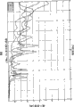
图6是连接器500中的四个差分信号触头对504所呈现的差分插入损耗与频率关系的比较曲线图600。如图6所示,连接器500可以在4到6GHz的频率范围中呈现大约-1.5分贝的插入损耗吸出。FIG. 6 is a comparative graph 600 of differential insertion loss versus frequency exhibited by four differential signal contact pairs 504 in connector 500 . As shown in FIG. 6, the connector 500 may exhibit an insertion loss draw of approximately -1.5 dB in the frequency range of 4 to 6 GHz.

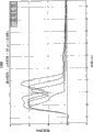
图7是连接器500中的四个差分信号触头对504所呈现的差分阻抗与时间关系的比较曲线图700。如图7所示,连接器500可以呈现大约100欧姆加或减6%的差分阻抗。FIG. 7 is a comparative graph 700 of differential impedance versus time exhibited by the four differential signal contact pairs 504 in the connector 500 . As shown in FIG. 7, connector 500 may exhibit a differential impedance of approximately 100 ohms plus or minus 6%.

图8是汇总连接器500中的四个差分信号触头对504所呈现的多有源的最坏情况串扰的表格800。如图8所示,连接器500可以呈现在大约2.6%到5.5%的范围内的多有源的最坏情况串扰。远端串扰显示在图8的上部两个象限内,而近端串扰显示在图8的下部两个象限内。尽管上升时间示出为50(10-90%)皮秒,但是该测量可以在35-1000(10-90%或20-80%)皮秒之间。这些值大体上可以对应于大约一百亿比特每秒或更多至小于622百万比特每秒。FIG. 8 is a table 800 summarizing the multi-active worst-case crosstalk exhibited by the four differential signal contact pairs 504 in the connector 500 . As shown in FIG. 8, connector 500 may exhibit multi-active worst-case crosstalk in the range of approximately 2.6% to 5.5%. FEXT is shown in the upper two quadrants of Figure 8, while NEXT is shown in the lower two quadrants of Figure 8. Although the rise time is shown as 50 (10-90%) picoseconds, the measurement may be between 35-1000 (10-90% or 20-80%) picoseconds. These values may generally correspond to about ten gigabits per second or more to less than 622 megabits per second.

图9A和9B描述了根据另一实施例的一个连接器900的等距视图。图9C描述了从连接器900的正面观察的触头布置902,触头布置902包括电触头502的线阵。类似于连接器500,连接器900可以没有接地板和/或串扰屏蔽。连接器900可以是安装到印刷电路板510上的直角连接器,然而可以理解,在替代实施例中,连接器900可以是垂直连接器。9A and 9B depict isometric views of a connector 900 according to another embodiment. FIG. 9C depicts a contact arrangement 902 comprising a linear array of electrical contacts 502 as viewed from the front of the connector 900 . Similar to connector 500, connector 900 may lack a ground plane and/or crosstalk shield. Connector 900 may be a right angle connector mounted to printed circuit board 510, however it will be appreciated that in alternative embodiments, connector 900 may be a vertical connector.

该连接器900通常可以包括与连接器500相同的特征和/或元件,诸如一个或多个用于容纳电触头502的线阵的引线框组件(未示出)和设置于相邻的信号触头S之间的电介质材料508。如图9A和9B所示,电介质材料508可以沿每一差分信号触头对504中的相应信号触头S的长度延伸,另外,连接器900可以与连接器500具有相同或类似的触头和触头间隔尺寸。The connector 900 may generally include the same features and/or elements as the connector 500, such as one or more lead frame assemblies (not shown) for accommodating the bar array of electrical contacts 502 and adjacent signal contacts. Dielectric material 508 between contacts S. As shown in FIGS. 9A and 9B , the dielectric material 508 can extend along the length of the corresponding signal contact S in each differential signal contact pair 504. In addition, the connector 900 can have the same or similar contacts and contacts as the connector 500. Contact spacing dimensions.

如图9C所示,连接器900与连接器500的不同可以在于连接器900可以没有任何接地触头G。更具体地,触头布置902可以包括一个或多个沿列526、528、530、532、534、536、538、540、542中的每一列成窄边对窄边布置的信号触头S。另外,该信号触头S可以沿行516、518、520、522、524中的每一行成宽边对宽边布置。行516、518、520、522、524中的每一行中的相邻信号触头S可以形成差分信号触头对504。与连接器500不同,接地触头G可以不设置于连接器900的行516、518、520、522、524中的每一差分信号触头对504之间。As shown in FIG. 9C , the connector 900 may be different from the connector 500 in that the connector 900 may not have any ground contact G. As shown in FIG. More specifically, the contact arrangement 902 may include one or more signal contacts S arranged edge-to-edge along each of the columns 526 , 528 , 530 , 532 , 534 , 536 , 538 , 540 , 542 . Additionally, the signal contacts S may be arranged broadside-to-broadside along each of the rows 516 , 518 , 520 , 522 , 524 . Adjacent signal contacts S in each of rows 516 , 518 , 520 , 522 , 524 may form differential signal contact pairs 504 . Unlike connector 500 , ground contacts G may not be disposed between each pair of differential signal contacts 504 in rows 516 , 518 , 520 , 522 , 524 of connector 900 .

图10是连接器900中的四个差分信号触头对504所呈现的差分插入损耗与频率关系的比较曲线图1000。如图10所示,连接器900可以在4到6GHz频率范围呈现出大约-0.5dB的插入损耗吸出。FIG. 10 is a comparative graph 1000 of differential insertion loss versus frequency exhibited by four differential signal contact pairs 504 in connector 900 . As shown in FIG. 10, the connector 900 may exhibit an insertion loss draw of approximately -0.5 dB in the 4 to 6 GHz frequency range.

图11是连接器900中的四个差分信号触头对504所呈现的差分阻抗与时间关系的比较曲线图1100。如图11所示,除一个以外的所有差分信号触头对504的差分阻抗可以是大约100欧姆加或减10%。可以理解,可以调整差分阻抗(即,匹配至系统阻抗),上述调整可以通过将形成差分信号触头对504的信号触头S移得更靠近或更远离、通过增加或减小信号触头S的宽度和/或通过增加或减小在信号触头S间的间隙中的介电常数来实现。FIG. 11 is a comparative graph 1100 of differential impedance versus time exhibited by four differential signal contact pairs 504 in connector 900 . As shown in FIG. 11 , the differential impedance of all but one of the differential signal contact pairs 504 may be approximately 100 ohms plus or minus 10%. It will be appreciated that the differential impedance (i.e., matched to the system impedance) can be adjusted by moving the signal contacts S forming the differential signal contact pair 504 closer or farther apart, by increasing or decreasing the signal contacts S width and/or by increasing or decreasing the dielectric constant in the gap between the signal contacts S.

图12是汇总了连接器900中的四个差分信号触头对504所呈现的多有源的最坏情况串扰的表格1200。如图12所示,连接器900可以呈现出位于大约2.7%到4.1%范围内的多有源的最坏情况串扰。远端串扰显示在图12的上部两个象限内,近端串扰显示在图12的下部两个象限内。FIG. 12 is a table 1200 summarizing the multi-active worst-case crosstalk exhibited by the four differential signal contact pairs 504 in the connector 900 . As shown in FIG. 12, connector 900 may exhibit multi-active worst-case crosstalk in the range of approximately 2.7% to 4.1%. FEXT is shown in the upper two quadrants of Figure 12, and NEXT is shown in the lower two quadrants of Figure 12.

图13A和13B描述了根据另一实施例的连接器1300的等距视图。图13C描述了连接器1300的后视图。图13D描述了从连接器1300的正面观察得触头布置1302,触头布置1302包括电触头502的线阵。类似于连接器500,连接器1300可以没有接地板和/或串扰屏蔽。连接器1300可以是安装到印刷电路板510上的直角连接器,然而可以理解,在替代实施例中,该连接器1300可以是垂直连接器。13A and 13B depict isometric views of a connector 1300 according to another embodiment. FIG. 13C depicts a rear view of connector 1300 . FIG. 13D depicts a contact arrangement 1302 comprising a linear array of electrical contacts 502 as viewed from the front of the connector 1300 . Similar to connector 500, connector 1300 may lack a ground plane and/or crosstalk shield. Connector 1300 may be a right angle connector mounted to printed circuit board 510, however it will be appreciated that in alternative embodiments, connector 1300 may be a vertical connector.

连接器1300通常可以包括与连接器500相同的特征和/或元件,诸如是一个或多个用于容纳电触头502的线阵的引线框组件(未示出)。每个线阵可以包括接地触头G和信号触头S。另外,连接器1300可以具有与连接器500相同或类似的触头和触头间隔尺寸,以及相同或类似的触头布置。Connector 1300 may generally include the same features and/or elements as connector 500 , such as one or more leadframe assemblies (not shown) for receiving the bar array of electrical contacts 502 . Each bar may include ground contacts G and signal contacts S. Additionally, connector 1300 may have the same or similar contact and contact spacing dimensions, and the same or similar contact arrangement as connector 500 .

如图13D所示,连接器1300与连接器500的不同可以在于该连接器1300可以不包括设置于形成差分信号触头对504的相邻信号触头S之间的电介质材料508。此外,行与行中心线的间隔K可以是大约1.4mm到3mm,优选地为1.65mm到2mm。列与列中心线的间隔L为大约1.3mm到2.5mm,优选地为1.4mm到1.5mm。As shown in FIG. 13D , connector 1300 may differ from connector 500 in that connector 1300 may not include dielectric material 508 disposed between adjacent signal contacts S forming differential signal contact pair 504 . In addition, the row-to-row centerline spacing K may be about 1.4mm to 3mm, preferably 1.65mm to 2mm. The column-to-column centerline spacing L is about 1.3mm to 2.5mm, preferably 1.4mm to 1.5mm.

图14是连接器1300中的四个差分信号触头对504所呈现的差分插入损耗与频率关系的比较曲线图1400。如图14所示,连接器1300可以在高达20GHz的频率呈现出小于-0.5dB的插入损耗,以及在0到20GHz的频率范围呈现出大约为零的吸出。另外,该插入损耗值表明在0到20GHz频率范围中最小限度的逐渐缩减。因此,一个或多个差分信号触头对504的插入损耗可以在直到至少40GHz保持在-2dB或更少。FIG. 14 is a comparative graph 1400 of differential insertion loss versus frequency exhibited by four differential signal contact pairs 504 in connector 1300 . As shown in FIG. 14, connector 1300 may exhibit an insertion loss of less than -0.5 dB at frequencies up to 20 GHz, and approximately zero draw-out at frequencies ranging from 0 to 20 GHz. Additionally, the insertion loss values show minimal tapering in the 0 to 20 GHz frequency range. Accordingly, the insertion loss of the one or more differential signal contact pairs 504 can be maintained at -2 dB or less up to at least 40 GHz.

图15是连接器1300中的四个差分信号触头对504所呈现的差分阻抗与时间关系的比较曲线图1500。如图15所示,除一个以外的所有差分信号触头对504的差分阻抗可以是大约100欧姆加或减10%。如上所述,可以调整差分阻抗(即,匹配至系统阻抗),上述调整可以通过将形成差分信号触头对504的信号触头S移得更靠近或更远离、通过增加或减小信号触头S的宽度和/或通过增加或减小在信号触头S间的间隙中的介电常数来实现。FIG. 15 is a comparative graph 1500 of differential impedance versus time exhibited by four differential signal contact pairs 504 in connector 1300 . As shown in FIG. 15, the differential impedance of all but one of the differential signal contact pairs 504 may be approximately 100 ohms plus or minus 10%. As described above, the differential impedance (i.e., matched to the system impedance) can be adjusted by moving the signal contacts S forming the differential signal contact pair 504 closer or farther apart, by increasing or decreasing the signal contacts S The width of S and/or is achieved by increasing or decreasing the dielectric constant in the gap between signal contacts S.

图16是汇总了连接器1300中的四个差分信号触头对504所呈现的多有源的最坏情况串扰的表1600。如图16所示,连接器1300可以呈现出位于大约0.3%到2.1%范围内的多有源的最坏情况串扰。远端串扰显示在图16的上部两个象限内,近端串扰显示在图16的下部两个象限内。FIG. 16 is a table 1600 summarizing the multi-active worst-case crosstalk exhibited by the four differential signal contact pairs 504 in the connector 1300 . As shown in FIG. 16, connector 1300 may exhibit multi-active worst case crosstalk in the range of approximately 0.3% to 2.1%. FEXT is shown in the upper two quadrants of Figure 16, and NEXT is shown in the lower two quadrants of Figure 16.

在一个或多个上述实施例中,至少一部分电触头可以被插入模制在塑料中。另外,该电连接器可以配置为用于平岩(flat rock)PCB的压配插入。例如,电触头的一个或多个线阵可以分层。然后可以将每个层压的线阵组合到一起以形成实体或单独的晶片的集合。替代地,可以制造具有四、五或六个边的盒子来围绕电触头。盒的内部可以填充有空气、塑料、PCB材料或它们的任意组合。可以经由焊球、可熔元件、焊料填角等将电连接器安装到印刷电路板上。In one or more of the above embodiments, at least a portion of the electrical contacts may be insert molded in plastic. Additionally, the electrical connector can be configured for press-fit insertion into a flat rock PCB. For example, one or more bars of electrical contacts may be layered. Each laminated bar can then be combined together to form a solid or collection of individual wafers. Alternatively, boxes with four, five or six sides can be fabricated to surround the electrical contacts. The interior of the box can be filled with air, plastic, PCB material or any combination thereof. Electrical connectors may be mounted to printed circuit boards via solder balls, fusible elements, solder fillets, and the like.

图17描述了从根据另一实施例的电连接器的正面观察的触头布置1700,其中差分信号触头成窄边对窄边布置。该触头布置1700可以包括电触头1732的线阵,其可以包括接地触头G和信号触头S。如图17所示,电触头1732可以布置成6×9的阵列并可以定义触头行1702、1704、1706、1708、1710、1712和触头列1714、1716、1718、1720、1722、1724、1726、1728、1730,然而,任何合适的配置可以适合于实施例。每列1714、1716、1718、1720、1722、1724、1726、1728、1730可以对应于IMLA。如图17所示,连接器中的每个电触头1732可以具有横截面,其定义了两个相对的窄边和两个相对的宽边。如图17进一步所示,接地触头G的宽边可以大于信号触头S的宽边。例如,在实施例中,地触头G的宽边可以比信号触头S的宽边大大约两倍。FIG. 17 depicts a contact arrangement 1700 viewed from the front of an electrical connector according to another embodiment, in which differential signal contacts are arranged edge-to-edge. The contact arrangement 1700 may include a linear array of electrical contacts 1732, which may include ground contacts G and signal contacts S. FIG. As shown in FIG. 17 , electrical contacts 1732 may be arranged in a 6×9 array and may define contact rows 1702 , 1704 , 1706 , 1708 , 1710 , 1712 and contact columns 1714 , 1716 , 1718 , 1720 , 1722 , 1724 , 1726, 1728, 1730, however, any suitable configuration may be suitable for an embodiment. Each column 1714, 1716, 1718, 1720, 1722, 1724, 1726, 1728, 1730 may correspond to an IMLA. As shown in FIG. 17, each electrical contact 1732 in the connector may have a cross-section that defines two opposing narrow sides and two opposing broad sides. As further shown in FIG. 17 , the broadsides of the ground contacts G may be larger than the broadsides of the signal contacts S . For example, in an embodiment, the broadside of the ground contact G may be about twice larger than the broadside of the signal contact S. Referring to FIG.

电触头1732可以沿列1714、1716、1718、1720、1722、1724、1726、1728、1730中的每一列成窄边对窄边布置。另外,至少一部分电触头1732可以沿行1702、1704、1706、1708、1710、1712中的每一行成宽边对宽边布置。列1714、1716、1718、1720、1722、1724、1726、1728、1730中的每一列中的相邻的信号触头S可以形成差分信号触头对1734。接地触头G可以设置于列1714、1716、1718、1720、1722、1724、1726、1728、1730中的每一差分信号触头对1734之间。接地触头G和信号触头S的所有侧面可以由电介质506围绕。The electrical contacts 1732 may be arranged edge-to-edge along each of the columns 1714 , 1716 , 1718 , 1720 , 1722 , 1724 , 1726 , 1728 , 1730 . Additionally, at least a portion of the electrical contacts 1732 may be arranged broadside-to-broadside along each of the rows 1702 , 1704 , 1706 , 1708 , 1710 , 1712 . Adjacent signal contacts S in each of columns 1714 , 1716 , 1718 , 1720 , 1722 , 1724 , 1726 , 1728 , 1730 may form differential signal contact pairs 1734 . Ground contacts G may be disposed between each differential signal contact pair 1734 in columns 1714 , 1716 , 1718 , 1720 , 1722 , 1724 , 1726 , 1728 , 1730 . All sides of the ground contact G and the signal contact S may be surrounded by a dielectric 506 .

触头列1714、1716、1718、1720、1722、1724、1726、1728、1730中的每一列可以定义触头式样。例如,列1714中的电触头1732可以布置(自顶部至底部移动)成G-S-S-G-S-S式样。列1716中的电触头1732可以布置成S-S-G-S-S-G式样,然而可以理解,当自底部至顶部观察时,列1716中的触头式样可以与列1714中的触头式样相同。列1718中的电触头1732可以布置成S-G-S-S-G-S式样,其可以不同于列1714、1716中的相应的触头式样。Each of the contact columns 1714, 1716, 1718, 1720, 1722, 1724, 1726, 1728, 1730 may define a contact pattern. For example, electrical contacts 1732 in column 1714 may be arranged (moving from top to bottom) in a G-S-S-G-S-S pattern. The electrical contacts 1732 in column 1716 may be arranged in an S-S-G-S-S-G pattern, however it is understood that the contact pattern in column 1716 may be the same as the contact pattern in column 1714 when viewed from bottom to top. The electrical contacts 1732 in column 1718 may be arranged in an S-G-S-S-G-S pattern, which may be different from the corresponding contact pattern in columns 1714 , 1716 .

可以在其余列中重复列1714、1716、1718中的触头式样,即,列1720可以与列1714具有相同的触头式样,列1722可以与列1716具有相同的触头式样,列1724可以与列1718具有相同的触头式样,等等。可以理解,一些信号触头S可以为中性触头或“额外插脚”,并且对于形成差分信号触头对1734不是必须的。The contact pattern in columns 1714, 1716, 1718 may be repeated in the remaining columns, i.e., column 1720 may have the same contact pattern as column 1714, column 1722 may have the same contact pattern as column 1716, and column 1724 may have the same contact pattern as column 1716. Columns 1718 have the same contact pattern, and so on. It will be appreciated that some of the signal contacts S may be neutral contacts or “extra pins” and are not required to form differential signal contact pair 1734 .

如图17所示,行1702、1704、1706、1708、1710、1712中的接地触头G可以形成由虚线1736定义的一个或多个阵列。例如,线1736之一可以从列1716中的接地触头G的一个侧面上的大约中心点处延伸到列1726中的另一接地触头G的相同侧面上的大约中心点处。可以理解,虚线1736可以从接地触头G的相同侧面上的任何合适的点延伸。每一虚线1736可以相对于列1714、1716、1718、1720、1722、1724、1726、1728、1730的方向定义斜角。每一线1736定义的斜角可以基本相同或彼此不同。As shown in FIG. 17 , ground contacts G in rows 1702 , 1704 , 1706 , 1708 , 1710 , 1712 may form one or more arrays defined by dashed lines 1736 . For example, one of lines 1736 may extend from approximately a center point on one side of ground contact G in column 1716 to approximately a center point on the same side of another ground contact G in column 1726 . It will be appreciated that the dashed line 1736 may extend from any suitable point on the same side of the ground contact G. Each dashed line 1736 may define an oblique angle with respect to the orientation of columns 1714 , 1716 , 1718 , 1720 , 1722 , 1724 , 1726 , 1728 , 1730 . The bevel angles defined by each line 1736 may be substantially the same or different from each other.

Claims (25)

1, a kind of electric connector comprises:
Become first electrical contact and second electrical contact of narrow limit along first direction to narrow limit layout;
Along second direction three electrical contact adjacent with described first electrical contact of the basic described first direction of crosscut, wherein, described first becomes broadside to the broadside layout and define first pair of differential signal contacts with the 3rd electrical contact; And
Along described second direction four electrical contact adjacent with described second electrical contact, wherein, described second becomes broadside that second pair of differential signal contacts arranged and defined to broadside with the 4th electrical contact, and
Wherein, described first and second pairs of differential signal contacts are offset each other along described second direction.
2, electric connector as claimed in claim 1 further comprises:
Be arranged at first non-air dielectric between the described first and the 3rd electrical contact of described first pair of differential signal contacts and be arranged at second non-air dielectric between the described second and the 4th electrical contact of described second pair of differential signal contacts.
3, electric connector as claimed in claim 2 wherein, comprises one of at least plastic material in described first or second non-air dielectric.
4, electric connector as claimed in claim 2, wherein, the described first and the 3rd electrical contact is contained in respectively in first lead frame assembly and second lead frame assembly, and
Wherein, it is molded that described first non-air dielectric is independent of described first and second lead frame assemblies.
5, electric connector as claimed in claim 1 further comprises:
First grounding contact adjacent with described first electrical contact, wherein, described first grounding contact becomes narrow limit that narrow limit is arranged with described first electrical contact along described first direction;
Second grounding contact adjacent with described the 3rd electrical contact, wherein, described second grounding contact becomes narrow limit that narrow limit is arranged with described the 3rd electrical contact along described first direction.
6, electric connector as claimed in claim 5, wherein, the broadside one of at least in described first and second grounding contacts is longer than the broadside one of at least in the described first and the 3rd electrical contact on described first direction.
7, electric connector as claimed in claim 1, wherein, described second electrical contact of described first electrical contact of described first pair of differential signal contacts and described second pair of differential signal contacts forms at least a portion with respect to the contact array at described first direction definition oblique angle.
8, electric connector as claimed in claim 1, wherein, described electric connector does not have screen.
9, electric connector as claimed in claim 1, wherein, described first electrical contact comprises first abutting end and first terminals, and defines first lengths of contacts betwixt;
Wherein, described the 3rd electrical contact comprises second abutting end and second terminals, and defines second lengths of contacts betwixt; And
Wherein, described first and second lengths of contacts are equal substantially.
10, electric connector as claimed in claim 1, in wherein said first and second pairs of differential signal contacts one of at least in the insertion loss that has up to the 20GHz frequency less than-0.5dB.
11, electric connector as claimed in claim 1, wherein, having in 0 to 20GHz scope one of at least in described first and second pairs of differential signal contacts is approximately zero sucking-off.
12, a kind of electric connector comprises:
First linear array of the electrical contact that extends along first direction, wherein, described first linear array comprises into first electrical contact and second electrical contact that broadside is arranged broadside, and wherein, described first and second electrical contacts form first pair of differential signal contacts; And
Second linear array of and electrical contact that along described first direction extend adjacent with described first linear array, wherein, described second linear array comprises into the 3rd electrical contact and the 4th electrical contact that broadside is arranged broadside,
Wherein, described third and fourth electrical contact forms second pair of differential signal contacts,
Wherein, described first and second pairs of differential signal contacts are offset each other along described first direction, and
Wherein, described second electrical contact and described the 3rd electrical contact become narrow limit that narrow limit is arranged being basically perpendicular on the second direction of described first direction.
13, electric connector as claimed in claim 12 further comprises:
Be arranged at first non-air dielectric between described first and second electrical contacts; And
Be arranged at second non-air dielectric between described third and fourth electrical contact.
14, electric connector as claimed in claim 13, wherein, described first and second electrical contacts are contained in respectively in first lead frame assembly and second lead frame assembly, and
Wherein, described first non-air dielectric forms as the part one of at least in described first or second lead frame assembly.
15, electric connector as claimed in claim 12 further comprises grounding contact, and described grounding contact is adjacent with described first electrical contact along described second direction, and adjacent with described the 3rd electrical contact along described first direction.
16, electric connector as claimed in claim 15, wherein, described grounding contact becomes narrow limit that narrow limit is arranged with described first electrical contact, and
Wherein, described grounding contact becomes broadside that broadside is arranged with described the 3rd electrical contact.
17, electric connector as claimed in claim 15, wherein, the broadside of described grounding contact is longer than the broadside one of at least in the described first and the 3rd electrical contact on described second direction.
18, electric connector as claimed in claim 12 wherein, one of at least is configured to make signal skew to minimize in described first or second pair of differential signal contacts.
19, electric connector as claimed in claim 12, wherein, described electric connector does not have screen.
20, a kind of electric connector comprises:
Define first linear array of the electrical contact of the first contact style along first direction;
Second linear array of the electrical contact adjacent with described first linear array, wherein, described second linear array defines the second contact style along the second direction opposite with described first direction, and wherein, the described first and second contact styles are basic identical; And
The 3rd linear array of the electrical contact adjacent with described second linear array, wherein, described the 3rd linear array along described first or second direction define the 3rd contact style, wherein, described the 3rd contact style is different from the described first and second contact styles, and described first, second repeats in the adjacent linear array of electrical contact with the 3rd style.
21, electric connector as claimed in claim 20 further comprises in described first, second and the 3rd linear array of electrical contact each most air dielectric.
22, electric connector as claimed in claim 20, wherein, described first linear array comprises into more than first electrical contact that narrow limit is arranged narrow limit,
Wherein, described second linear array comprises into more than second electrical contact that narrow limit is arranged narrow limit,
Wherein, described the 3rd linear array comprises into more than the 3rd electrical contact that narrow limit is arranged narrow limit,
Wherein, first electrical contact of described first linear array and second electrical contact of described second linear array form first pair of differential signal contacts, and
Wherein, the 4th electrical contact of the 3rd electrical contact of described second linear array and described the 3rd linear array forms second pair of differential signal contacts.
23, electric connector as claimed in claim 22, wherein, described first and second pairs of differential signal contacts upwards are offset each other in the four directions that is basically perpendicular to described first direction.
24, electric connector as claimed in claim 22, wherein, described more than first electrical contact, described more than second contact and described more than the 3rd contact comprise first grounding contact, second grounding contact and the 3rd grounding contact respectively, and
Wherein, described first, second forms the array that defines the oblique angle with respect to described first direction with the 3rd grounding contact.
25, electric connector as claimed in claim 22, wherein, described first and second pairs of differential signal contacts form the array with respect to described first direction definition oblique angle.
CN2007800406013A 2006-10-30 2007-10-26 electrical connector Expired - Fee Related CN101536259B (en)

Applications Claiming Priority (9)

Application Number Priority Date Filing Date Title
US85555806P 2006-10-30 2006-10-30
US60/855,558 2006-10-30
US86929206P 2006-12-08 2006-12-08
US60/869,292 2006-12-08
US11/866,061 US7713088B2 (en) 2006-10-05 2007-10-02 Broadside-coupled signal pair configurations for electrical connectors
US11/866,061 2007-10-02
US11/924,002 2007-10-25
US11/924,002 US7708569B2 (en) 2006-10-30 2007-10-25 Broadside-coupled signal pair configurations for electrical connectors
PCT/US2007/022753 WO2008054683A1 (en) 2006-10-30 2007-10-26 Broadside-coupled signal pair configurations for electrical connectors

Related Child Applications (1)

Application Number Title Priority Date Filing Date
CN2010105261048A Division CN102064406B (en) 2006-10-30 2007-10-26 Broadside coupled signal pair configuration for electrical connectors

Publications (2)

Publication Number Publication Date
CN101536259A true CN101536259A (en) 2009-09-16
CN101536259B CN101536259B (en) 2011-11-09

Family

ID=39344588

Family Applications (2)

Application Number Title Priority Date Filing Date
CN2007800406013A Expired - Fee Related CN101536259B (en) 2006-10-30 2007-10-26 electrical connector
CN2010105261048A Expired - Fee Related CN102064406B (en) 2006-10-30 2007-10-26 Broadside coupled signal pair configuration for electrical connectors

Family Applications After (1)

Application Number Title Priority Date Filing Date
CN2010105261048A Expired - Fee Related CN102064406B (en) 2006-10-30 2007-10-26 Broadside coupled signal pair configuration for electrical connectors

Country Status (3)

Country Link
EP (1) EP2084785B1 (en)
CN (2) CN101536259B (en)
WO (1) WO2008054683A1 (en)

Cited By (3)

* Cited by examiner, † Cited by third party
Publication number Priority date Publication date Assignee Title
CN104737375A (en) * 2012-09-18 2015-06-24 罗森伯格高频技术有限及两合公司 Plug connection
CN106558806A (en) * 2015-09-30 2017-04-05 泰科电子(上海)有限公司 Adapter
CN109586107A (en) * 2017-09-29 2019-04-05 中航光电科技股份有限公司 Connector and signal transmission structure thereof

Families Citing this family (1)

* Cited by examiner, † Cited by third party
Publication number Priority date Publication date Assignee Title
US8715003B2 (en) * 2009-12-30 2014-05-06 Fci Americas Technology Llc Electrical connector having impedance tuning ribs

Family Cites Families (6)

* Cited by examiner, † Cited by third party
Publication number Priority date Publication date Assignee Title
US5224867A (en) * 1990-10-08 1993-07-06 Daiichi Denshi Kogyo Kabushiki Kaisha Electrical connector for coaxial flat cable
US5525067A (en) * 1994-02-03 1996-06-11 Motorola, Inc Ground plane interconnection system using multiple connector contacts
JP4373215B2 (en) * 2001-11-14 2009-11-25 エフシーアイ Crosstalk reduction for electrical connectors
US6652318B1 (en) * 2002-05-24 2003-11-25 Fci Americas Technology, Inc. Cross-talk canceling technique for high speed electrical connectors
US6692272B2 (en) * 2001-11-14 2004-02-17 Fci Americas Technology, Inc. High speed electrical connector
US6641411B1 (en) * 2002-07-24 2003-11-04 Maxxan Systems, Inc. Low cost high speed connector

Cited By (7)

* Cited by examiner, † Cited by third party
Publication number Priority date Publication date Assignee Title
CN104737375A (en) * 2012-09-18 2015-06-24 罗森伯格高频技术有限及两合公司 Plug connection
CN106558806A (en) * 2015-09-30 2017-04-05 泰科电子(上海)有限公司 Adapter
CN106558806B (en) * 2015-09-30 2019-03-01 泰科电子(上海)有限公司 Connector
CN109586107A (en) * 2017-09-29 2019-04-05 中航光电科技股份有限公司 Connector and signal transmission structure thereof
CN109586107B (en) * 2017-09-29 2020-09-18 中航光电科技股份有限公司 A connector and its signal transmission structure
CN112117605A (en) * 2017-09-29 2020-12-22 中航光电科技股份有限公司 Connector and signal transmission structure thereof
CN112117605B (en) * 2017-09-29 2022-03-11 中航光电科技股份有限公司 Connector and signal transmission structure thereof

Also Published As

Publication number Publication date
EP2084785A1 (en) 2009-08-05
EP2084785A4 (en) 2012-09-19
WO2008054683A1 (en) 2008-05-08
CN102064406B (en) 2013-07-31
CN101536259B (en) 2011-11-09
CN102064406A (en) 2011-05-18
EP2084785B1 (en) 2014-06-04

Similar Documents

Publication Publication Date Title
US7708569B2 (en) Broadside-coupled signal pair configurations for electrical connectors
US7713088B2 (en) Broadside-coupled signal pair configurations for electrical connectors
CN102598431B (en) Electrical connector with ground plate and ground bond bar
US7497736B2 (en) Shieldless, high-speed, low-cross-talk electrical connector
CN101395760B (en) High Density Orthogonal Connectors
US6652318B1 (en) Cross-talk canceling technique for high speed electrical connectors
US7837504B2 (en) Impedance mating interface for electrical connectors
CN102460849B (en) Low crosstalk electrical connector
CN101611521B (en) Unshielded, high-speed, low-crosstalk electrical connector
CN102684009B (en) Electrical connectors with common ground shield
CN101395768A (en) Broadside-to-Edge Coupled Connector System
US8734187B2 (en) Electrical connector with ground plates
CN101536259B (en) electrical connector
CN109348736B (en) Orthogonal Electrical Connector Assembly
TWI550971B (en) Shieldless, high-speed, low-cross-talk electrical connector
CN101523669B (en) Broadside coupled signal pair construction for electrical connectors

Legal Events

Date Code Title Description
C06 Publication
PB01 Publication
C10 Entry into substantive examination
SE01 Entry into force of request for substantive examination
C14 Grant of patent or utility model
GR01 Patent grant
CF01 Termination of patent right due to non-payment of annual fee

Granted publication date: 20111109

Termination date: 20161026

CF01 Termination of patent right due to non-payment of annual fee