CN101527280B - Semiconductor structure and manufacturing method thereof - Google Patents
Semiconductor structure and manufacturing method thereof Download PDFInfo
- Publication number
- CN101527280B CN101527280B CN2008101356836A CN200810135683A CN101527280B CN 101527280 B CN101527280 B CN 101527280B CN 2008101356836 A CN2008101356836 A CN 2008101356836A CN 200810135683 A CN200810135683 A CN 200810135683A CN 101527280 B CN101527280 B CN 101527280B
- Authority
- CN
- China
- Prior art keywords
- material layer
- silicon
- layer
- gate dielectric
- silicon germanium
- Prior art date
- Legal status (The legal status is an assumption and is not a legal conclusion. Google has not performed a legal analysis and makes no representation as to the accuracy of the status listed.)
- Expired - Fee Related
Links
- 239000004065 semiconductor Substances 0.000 title claims abstract description 58
- 238000004519 manufacturing process Methods 0.000 title claims abstract description 26
- 239000000463 material Substances 0.000 claims abstract description 145
- 229910000577 Silicon-germanium Inorganic materials 0.000 claims abstract description 129
- LEVVHYCKPQWKOP-UHFFFAOYSA-N [Si].[Ge] Chemical compound [Si].[Ge] LEVVHYCKPQWKOP-UHFFFAOYSA-N 0.000 claims abstract description 116
- 239000002210 silicon-based material Substances 0.000 claims abstract description 50
- 238000000034 method Methods 0.000 claims abstract description 29
- 239000000758 substrate Substances 0.000 claims abstract description 20
- 238000000059 patterning Methods 0.000 claims abstract description 11
- 229910052710 silicon Inorganic materials 0.000 claims description 29
- 239000010703 silicon Substances 0.000 claims description 29
- XUIMIQQOPSSXEZ-UHFFFAOYSA-N Silicon Chemical compound [Si] XUIMIQQOPSSXEZ-UHFFFAOYSA-N 0.000 claims description 25
- 229910052732 germanium Inorganic materials 0.000 claims description 18
- GNPVGFCGXDBREM-UHFFFAOYSA-N germanium atom Chemical compound [Ge] GNPVGFCGXDBREM-UHFFFAOYSA-N 0.000 claims description 18
- 229910052782 aluminium Inorganic materials 0.000 claims description 13
- XAGFODPZIPBFFR-UHFFFAOYSA-N aluminium Chemical compound [Al] XAGFODPZIPBFFR-UHFFFAOYSA-N 0.000 claims description 13
- 229910052746 lanthanum Inorganic materials 0.000 claims description 11
- FZLIPJUXYLNCLC-UHFFFAOYSA-N lanthanum atom Chemical compound [La] FZLIPJUXYLNCLC-UHFFFAOYSA-N 0.000 claims description 11
- 239000007769 metal material Substances 0.000 description 14
- 230000015572 biosynthetic process Effects 0.000 description 10
- 229910052751 metal Inorganic materials 0.000 description 10
- 239000002184 metal Substances 0.000 description 10
- 229910052735 hafnium Inorganic materials 0.000 description 7
- VBJZVLUMGGDVMO-UHFFFAOYSA-N hafnium atom Chemical compound [Hf] VBJZVLUMGGDVMO-UHFFFAOYSA-N 0.000 description 7
- 239000004411 aluminium Substances 0.000 description 6
- 238000005229 chemical vapour deposition Methods 0.000 description 6
- VYPSYNLAJGMNEJ-UHFFFAOYSA-N Silicium dioxide Chemical compound O=[Si]=O VYPSYNLAJGMNEJ-UHFFFAOYSA-N 0.000 description 5
- 238000002955 isolation Methods 0.000 description 5
- 230000000295 complement effect Effects 0.000 description 4
- 238000004518 low pressure chemical vapour deposition Methods 0.000 description 4
- 238000000623 plasma-assisted chemical vapour deposition Methods 0.000 description 4
- 150000003376 silicon Chemical class 0.000 description 4
- 239000002253 acid Substances 0.000 description 3
- 238000000231 atomic layer deposition Methods 0.000 description 3
- 238000000151 deposition Methods 0.000 description 3
- 230000008021 deposition Effects 0.000 description 3
- 238000005530 etching Methods 0.000 description 3
- 230000001936 parietal effect Effects 0.000 description 3
- 229910052721 tungsten Inorganic materials 0.000 description 3
- 239000010937 tungsten Substances 0.000 description 3
- ZOKXTWBITQBERF-UHFFFAOYSA-N Molybdenum Chemical compound [Mo] ZOKXTWBITQBERF-UHFFFAOYSA-N 0.000 description 2
- KJTLSVCANCCWHF-UHFFFAOYSA-N Ruthenium Chemical compound [Ru] KJTLSVCANCCWHF-UHFFFAOYSA-N 0.000 description 2
- 229910052581 Si3N4 Inorganic materials 0.000 description 2
- BLRPTPMANUNPDV-UHFFFAOYSA-N Silane Chemical compound [SiH4] BLRPTPMANUNPDV-UHFFFAOYSA-N 0.000 description 2
- MCMNRKCIXSYSNV-UHFFFAOYSA-N ZrO2 Inorganic materials O=[Zr]=O MCMNRKCIXSYSNV-UHFFFAOYSA-N 0.000 description 2
- GPBUGPUPKAGMDK-UHFFFAOYSA-N azanylidynemolybdenum Chemical compound [Mo]#N GPBUGPUPKAGMDK-UHFFFAOYSA-N 0.000 description 2
- 239000007789 gas Substances 0.000 description 2
- 239000012535 impurity Substances 0.000 description 2
- 239000012212 insulator Substances 0.000 description 2
- 229910001092 metal group alloy Inorganic materials 0.000 description 2
- 229910044991 metal oxide Inorganic materials 0.000 description 2
- 150000004706 metal oxides Chemical class 0.000 description 2
- 229910052750 molybdenum Inorganic materials 0.000 description 2
- 239000011733 molybdenum Substances 0.000 description 2
- RVTZCBVAJQQJTK-UHFFFAOYSA-N oxygen(2-);zirconium(4+) Chemical compound [O-2].[O-2].[Zr+4] RVTZCBVAJQQJTK-UHFFFAOYSA-N 0.000 description 2
- 238000005240 physical vapour deposition Methods 0.000 description 2
- 229910052707 ruthenium Inorganic materials 0.000 description 2
- 239000000377 silicon dioxide Substances 0.000 description 2
- HQVNEWCFYHHQES-UHFFFAOYSA-N silicon nitride Chemical compound N12[Si]34N5[Si]62N3[Si]51N64 HQVNEWCFYHHQES-UHFFFAOYSA-N 0.000 description 2
- 229910052715 tantalum Inorganic materials 0.000 description 2
- GUVRBAGPIYLISA-UHFFFAOYSA-N tantalum atom Chemical compound [Ta] GUVRBAGPIYLISA-UHFFFAOYSA-N 0.000 description 2
- -1 tungsten nitride Chemical class 0.000 description 2
- 206010010144 Completed suicide Diseases 0.000 description 1
- DLIJBCLXWXVWHF-UHFFFAOYSA-N [N].[Ta].[Si] Chemical compound [N].[Ta].[Si] DLIJBCLXWXVWHF-UHFFFAOYSA-N 0.000 description 1
- CEPICIBPGDWCRU-UHFFFAOYSA-N [Si].[Hf] Chemical compound [Si].[Hf] CEPICIBPGDWCRU-UHFFFAOYSA-N 0.000 description 1
- WIGAYVXYNSVZAV-UHFFFAOYSA-N ac1lavbc Chemical compound [W].[W] WIGAYVXYNSVZAV-UHFFFAOYSA-N 0.000 description 1
- 239000013078 crystal Substances 0.000 description 1
- 238000010586 diagram Methods 0.000 description 1
- 239000003989 dielectric material Substances 0.000 description 1
- ZGHDMISTQPRNRG-UHFFFAOYSA-N dimolybdenum Chemical compound [Mo]#[Mo] ZGHDMISTQPRNRG-UHFFFAOYSA-N 0.000 description 1
- 230000000694 effects Effects 0.000 description 1
- 238000005516 engineering process Methods 0.000 description 1
- 229910000078 germane Inorganic materials 0.000 description 1
- QUZPNFFHZPRKJD-UHFFFAOYSA-N germane Chemical compound [GeH4] QUZPNFFHZPRKJD-UHFFFAOYSA-N 0.000 description 1
- 229910052986 germanium hydride Inorganic materials 0.000 description 1
- KUVFGOLWQIXGBP-UHFFFAOYSA-N hafnium(4+);oxygen(2-);titanium(4+) Chemical compound [O-2].[O-2].[O-2].[O-2].[Ti+4].[Hf+4] KUVFGOLWQIXGBP-UHFFFAOYSA-N 0.000 description 1
- CJNBYAVZURUTKZ-UHFFFAOYSA-N hafnium(iv) oxide Chemical compound O=[Hf]=O CJNBYAVZURUTKZ-UHFFFAOYSA-N 0.000 description 1
- 230000010354 integration Effects 0.000 description 1
- 238000002488 metal-organic chemical vapour deposition Methods 0.000 description 1
- 238000006396 nitration reaction Methods 0.000 description 1
- 238000012797 qualification Methods 0.000 description 1
- 229910001925 ruthenium oxide Inorganic materials 0.000 description 1
- WOCIAKWEIIZHES-UHFFFAOYSA-N ruthenium(iv) oxide Chemical compound O=[Ru]=O WOCIAKWEIIZHES-UHFFFAOYSA-N 0.000 description 1
- 229910000077 silane Inorganic materials 0.000 description 1
- 229910021332 silicide Inorganic materials 0.000 description 1
- FVBUAEGBCNSCDD-UHFFFAOYSA-N silicide(4-) Chemical group [Si-4] FVBUAEGBCNSCDD-UHFFFAOYSA-N 0.000 description 1
- 229910052814 silicon oxide Inorganic materials 0.000 description 1
- MZLGASXMSKOWSE-UHFFFAOYSA-N tantalum nitride Chemical compound [Ta]#N MZLGASXMSKOWSE-UHFFFAOYSA-N 0.000 description 1
- WFKWXMTUELFFGS-UHFFFAOYSA-N tungsten Chemical compound [W] WFKWXMTUELFFGS-UHFFFAOYSA-N 0.000 description 1
Images


Classifications
-
- H—ELECTRICITY
- H10—SEMICONDUCTOR DEVICES; ELECTRIC SOLID-STATE DEVICES NOT OTHERWISE PROVIDED FOR
- H10D—INORGANIC ELECTRIC SEMICONDUCTOR DEVICES
- H10D84/00—Integrated devices formed in or on semiconductor substrates that comprise only semiconducting layers, e.g. on Si wafers or on GaAs-on-Si wafers
- H10D84/80—Integrated devices formed in or on semiconductor substrates that comprise only semiconducting layers, e.g. on Si wafers or on GaAs-on-Si wafers characterised by the integration of at least one component covered by groups H10D12/00 or H10D30/00, e.g. integration of IGFETs
- H10D84/82—Integrated devices formed in or on semiconductor substrates that comprise only semiconducting layers, e.g. on Si wafers or on GaAs-on-Si wafers characterised by the integration of at least one component covered by groups H10D12/00 or H10D30/00, e.g. integration of IGFETs of only field-effect components
- H10D84/83—Integrated devices formed in or on semiconductor substrates that comprise only semiconducting layers, e.g. on Si wafers or on GaAs-on-Si wafers characterised by the integration of at least one component covered by groups H10D12/00 or H10D30/00, e.g. integration of IGFETs of only field-effect components of only insulated-gate FETs [IGFET]
- H10D84/85—Complementary IGFETs, e.g. CMOS
-
- H—ELECTRICITY
- H10—SEMICONDUCTOR DEVICES; ELECTRIC SOLID-STATE DEVICES NOT OTHERWISE PROVIDED FOR
- H10D—INORGANIC ELECTRIC SEMICONDUCTOR DEVICES
- H10D30/00—Field-effect transistors [FET]
- H10D30/01—Manufacture or treatment
- H10D30/021—Manufacture or treatment of FETs having insulated gates [IGFET]
- H10D30/027—Manufacture or treatment of FETs having insulated gates [IGFET] of lateral single-gate IGFETs
- H10D30/0275—Manufacture or treatment of FETs having insulated gates [IGFET] of lateral single-gate IGFETs forming single crystalline semiconductor source or drain regions resulting in recessed gates, e.g. forming raised source or drain regions
-
- H—ELECTRICITY
- H10—SEMICONDUCTOR DEVICES; ELECTRIC SOLID-STATE DEVICES NOT OTHERWISE PROVIDED FOR
- H10D—INORGANIC ELECTRIC SEMICONDUCTOR DEVICES
- H10D30/00—Field-effect transistors [FET]
- H10D30/60—Insulated-gate field-effect transistors [IGFET]
- H10D30/601—Insulated-gate field-effect transistors [IGFET] having lightly-doped drain or source extensions, e.g. LDD IGFETs or DDD IGFETs
-
- H—ELECTRICITY
- H10—SEMICONDUCTOR DEVICES; ELECTRIC SOLID-STATE DEVICES NOT OTHERWISE PROVIDED FOR
- H10D—INORGANIC ELECTRIC SEMICONDUCTOR DEVICES
- H10D30/00—Field-effect transistors [FET]
- H10D30/60—Insulated-gate field-effect transistors [IGFET]
- H10D30/751—Insulated-gate field-effect transistors [IGFET] having composition variations in the channel regions
-
- H—ELECTRICITY
- H10—SEMICONDUCTOR DEVICES; ELECTRIC SOLID-STATE DEVICES NOT OTHERWISE PROVIDED FOR
- H10D—INORGANIC ELECTRIC SEMICONDUCTOR DEVICES
- H10D30/00—Field-effect transistors [FET]
- H10D30/60—Insulated-gate field-effect transistors [IGFET]
- H10D30/791—Arrangements for exerting mechanical stress on the crystal lattice of the channel regions
- H10D30/797—Arrangements for exerting mechanical stress on the crystal lattice of the channel regions being in source or drain regions, e.g. SiGe source or drain
-
- H—ELECTRICITY
- H10—SEMICONDUCTOR DEVICES; ELECTRIC SOLID-STATE DEVICES NOT OTHERWISE PROVIDED FOR
- H10D—INORGANIC ELECTRIC SEMICONDUCTOR DEVICES
- H10D62/00—Semiconductor bodies, or regions thereof, of devices having potential barriers
- H10D62/01—Manufacture or treatment
- H10D62/021—Forming source or drain recesses by etching e.g. recessing by etching and then refilling
-
- H—ELECTRICITY
- H10—SEMICONDUCTOR DEVICES; ELECTRIC SOLID-STATE DEVICES NOT OTHERWISE PROVIDED FOR
- H10D—INORGANIC ELECTRIC SEMICONDUCTOR DEVICES
- H10D62/00—Semiconductor bodies, or regions thereof, of devices having potential barriers
- H10D62/10—Shapes, relative sizes or dispositions of the regions of the semiconductor bodies; Shapes of the semiconductor bodies
- H10D62/113—Isolations within a component, i.e. internal isolations
- H10D62/115—Dielectric isolations, e.g. air gaps
-
- H—ELECTRICITY
- H10—SEMICONDUCTOR DEVICES; ELECTRIC SOLID-STATE DEVICES NOT OTHERWISE PROVIDED FOR
- H10D—INORGANIC ELECTRIC SEMICONDUCTOR DEVICES
- H10D62/00—Semiconductor bodies, or regions thereof, of devices having potential barriers
- H10D62/10—Shapes, relative sizes or dispositions of the regions of the semiconductor bodies; Shapes of the semiconductor bodies
- H10D62/13—Semiconductor regions connected to electrodes carrying current to be rectified, amplified or switched, e.g. source or drain regions
- H10D62/149—Source or drain regions of field-effect devices
- H10D62/151—Source or drain regions of field-effect devices of IGFETs
-
- H—ELECTRICITY
- H10—SEMICONDUCTOR DEVICES; ELECTRIC SOLID-STATE DEVICES NOT OTHERWISE PROVIDED FOR
- H10D—INORGANIC ELECTRIC SEMICONDUCTOR DEVICES
- H10D62/00—Semiconductor bodies, or regions thereof, of devices having potential barriers
- H10D62/80—Semiconductor bodies, or regions thereof, of devices having potential barriers characterised by the materials
- H10D62/82—Heterojunctions
- H10D62/822—Heterojunctions comprising only Group IV materials heterojunctions, e.g. Si/Ge heterojunctions
-
- H—ELECTRICITY
- H10—SEMICONDUCTOR DEVICES; ELECTRIC SOLID-STATE DEVICES NOT OTHERWISE PROVIDED FOR
- H10D—INORGANIC ELECTRIC SEMICONDUCTOR DEVICES
- H10D84/00—Integrated devices formed in or on semiconductor substrates that comprise only semiconducting layers, e.g. on Si wafers or on GaAs-on-Si wafers
- H10D84/01—Manufacture or treatment
- H10D84/0123—Integrating together multiple components covered by H10D12/00 or H10D30/00, e.g. integrating multiple IGBTs
- H10D84/0126—Integrating together multiple components covered by H10D12/00 or H10D30/00, e.g. integrating multiple IGBTs the components including insulated gates, e.g. IGFETs
- H10D84/0165—Integrating together multiple components covered by H10D12/00 or H10D30/00, e.g. integrating multiple IGBTs the components including insulated gates, e.g. IGFETs the components including complementary IGFETs, e.g. CMOS devices
- H10D84/0167—Manufacturing their channels
-
- H—ELECTRICITY
- H10—SEMICONDUCTOR DEVICES; ELECTRIC SOLID-STATE DEVICES NOT OTHERWISE PROVIDED FOR
- H10D—INORGANIC ELECTRIC SEMICONDUCTOR DEVICES
- H10D84/00—Integrated devices formed in or on semiconductor substrates that comprise only semiconducting layers, e.g. on Si wafers or on GaAs-on-Si wafers
- H10D84/01—Manufacture or treatment
- H10D84/0123—Integrating together multiple components covered by H10D12/00 or H10D30/00, e.g. integrating multiple IGBTs
- H10D84/0126—Integrating together multiple components covered by H10D12/00 or H10D30/00, e.g. integrating multiple IGBTs the components including insulated gates, e.g. IGFETs
- H10D84/0165—Integrating together multiple components covered by H10D12/00 or H10D30/00, e.g. integrating multiple IGBTs the components including insulated gates, e.g. IGFETs the components including complementary IGFETs, e.g. CMOS devices
- H10D84/017—Manufacturing their source or drain regions, e.g. silicided source or drain regions
-
- H—ELECTRICITY
- H10—SEMICONDUCTOR DEVICES; ELECTRIC SOLID-STATE DEVICES NOT OTHERWISE PROVIDED FOR
- H10D—INORGANIC ELECTRIC SEMICONDUCTOR DEVICES
- H10D84/00—Integrated devices formed in or on semiconductor substrates that comprise only semiconducting layers, e.g. on Si wafers or on GaAs-on-Si wafers
- H10D84/01—Manufacture or treatment
- H10D84/0123—Integrating together multiple components covered by H10D12/00 or H10D30/00, e.g. integrating multiple IGBTs
- H10D84/0126—Integrating together multiple components covered by H10D12/00 or H10D30/00, e.g. integrating multiple IGBTs the components including insulated gates, e.g. IGFETs
- H10D84/0165—Integrating together multiple components covered by H10D12/00 or H10D30/00, e.g. integrating multiple IGBTs the components including insulated gates, e.g. IGFETs the components including complementary IGFETs, e.g. CMOS devices
- H10D84/0172—Manufacturing their gate conductors
- H10D84/0177—Manufacturing their gate conductors the gate conductors having different materials or different implants
-
- H—ELECTRICITY
- H10—SEMICONDUCTOR DEVICES; ELECTRIC SOLID-STATE DEVICES NOT OTHERWISE PROVIDED FOR
- H10D—INORGANIC ELECTRIC SEMICONDUCTOR DEVICES
- H10D84/00—Integrated devices formed in or on semiconductor substrates that comprise only semiconducting layers, e.g. on Si wafers or on GaAs-on-Si wafers
- H10D84/01—Manufacture or treatment
- H10D84/0123—Integrating together multiple components covered by H10D12/00 or H10D30/00, e.g. integrating multiple IGBTs
- H10D84/0126—Integrating together multiple components covered by H10D12/00 or H10D30/00, e.g. integrating multiple IGBTs the components including insulated gates, e.g. IGFETs
- H10D84/0165—Integrating together multiple components covered by H10D12/00 or H10D30/00, e.g. integrating multiple IGBTs the components including insulated gates, e.g. IGFETs the components including complementary IGFETs, e.g. CMOS devices
- H10D84/0181—Manufacturing their gate insulating layers
-
- H—ELECTRICITY
- H10—SEMICONDUCTOR DEVICES; ELECTRIC SOLID-STATE DEVICES NOT OTHERWISE PROVIDED FOR
- H10D—INORGANIC ELECTRIC SEMICONDUCTOR DEVICES
- H10D84/00—Integrated devices formed in or on semiconductor substrates that comprise only semiconducting layers, e.g. on Si wafers or on GaAs-on-Si wafers
- H10D84/01—Manufacture or treatment
- H10D84/02—Manufacture or treatment characterised by using material-based technologies
- H10D84/03—Manufacture or treatment characterised by using material-based technologies using Group IV technology, e.g. silicon technology or silicon-carbide [SiC] technology
- H10D84/038—Manufacture or treatment characterised by using material-based technologies using Group IV technology, e.g. silicon technology or silicon-carbide [SiC] technology using silicon technology, e.g. SiGe
Landscapes
- Metal-Oxide And Bipolar Metal-Oxide Semiconductor Integrated Circuits (AREA)
- Insulated Gate Type Field-Effect Transistor (AREA)
- Chemical & Material Sciences (AREA)
- Crystallography & Structural Chemistry (AREA)
Abstract
The invention provides a semiconductor structure and a manufacturing method thereof, wherein the method comprises the following steps: providing a semiconductor substrate, wherein the semiconductor substrate comprises a first area and a second area; forming a first MOS element comprising: forming a first SiGe layer on the first region of the semiconductor substrate; forming a silicon material layer on the first silicon germanium material layer; forming a first gate dielectric layer on the silicon material layer; and patterning the first gate dielectric layer to form a first gate dielectric structure. The method further includes forming a second MOS element, including: forming a second silicon germanium material layer on the second region of the semiconductor substrate; forming a second gate dielectric layer on the second SiGe layer, wherein the second SiGe layer and the second gate dielectric layer in the second MOS device do not have a substantially pure Si layer therebetween; and patterning the second gate dielectric layer to form a second gate dielectric structure. The invention can improve the drive current of the NMOS element and reduce the leakage current of the PMOS element.
Description
Technical field
The present invention is particularly to CMOS (Complementary Metal Oxide Semiconductor) device and manufacture method thereof relevant for a kind of semiconductor structure and manufacture method thereof.
Background technology
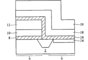
Fig. 1 to Fig. 5 is existing complementary MOS (complementary MOS, CMOS) Zhuan Zhi manufacturing process generalized section.Fig. 1 shows the silicon base 2 that comprises nmos area 4 and PMOS district 6.Code-pattern ground forms a high-dielectric coefficient gate dielectric 8 on silicon base 2.Then form N type metal level (N-metal layer) 10.Then form a hard mask 12, and patterned, to cover nmos area 4.In Fig. 2, dielectric layer 8 and N type metal level 10 in the PMOS district 6 are removed.Silicon base 2 in the PMOS district 6 also is removed to form a recess 7.As shown in Figure 3, follow extension formation silicon germanium material layer 14 in recess 7.Fig. 4 shows that the blanket property covered ground forms high-dielectric coefficient gate dielectric 16, P type metal level (P-metal layer) 18 and hard mask 19.Fig. 5 shows that high-dielectric coefficient gate dielectric 16, P type metal level 18 and the hard masks 19 followed in the nmos area 4 remove.
Shown stack layer can be used to form the NMOS element (not being shown in figure) that is arranged in nmos area 4 among Fig. 5, and the PMOS element (not being shown in figure) that is arranged in PMOS district 6.Therefore the channel region of formed PMOS element is to be formed by 14 on silicon germanium material layer.This helps the critical voltage of PMOS element (threshold voltage) is reduced.In addition, compare with the PMOS element with silicon raceway groove, its hole mobility of PMOS element with SiGe raceway groove is higher.Therefore can promote the drive current (drive current) that is formed at the PMOS element in the PMOS district 6.
Yet, its shortcoming is arranged with the formed cmos element of said method.Owing to be formed at the channel region of the NMOS element in the nmos area 4, there is no the stress of the substrate that comes from the channel region below, so the drive current of NMOS element be less than ideal value.Moreover, because the Ge element in the silicon germanium material layer 14 may diffuse to high-dielectric coefficient dielectric layer 16, therefore can in formed PMOS element, cause leakage current.Therefore need to promote the NMOS element drive current, and reduce the manufacture method of PMOS element leakage current.
Summary of the invention
The invention provides a kind of manufacture method of semiconductor structure, comprise the following steps.The semiconductor-based end is provided, and this semiconductor-based end, comprise first district and second district.Form a MOS element, comprising: go up in this first district at this semiconductor-based end and form the first silicon germanium material floor; On this first silicon germanium material layer, form silicon material layer; On this silicon material layer, form the first grid dielectric layer; And this first grid dielectric layer of patterning is to form the first grid dielectric structure.And form the 2nd MOS element, comprising: go up in this second district at this semiconductor-based end and form the second silicon germanium material floor; On this second silicon germanium material layer, form the second grid dielectric layer, wherein do not have pure silicon material layer substantially between this second silicon germanium material layer in the 2nd MOS element and this second grid dielectric layer; And this second grid dielectric layer of patterning is to form the second grid dielectric structure.
According to the manufacture method of above-mentioned semiconductor structure, preferably, also be included in form this second grid dielectric layer before, on this second silicon germanium material layer, form the 3rd silicon germanium material layer.
According to the manufacture method of above-mentioned semiconductor structure, preferably, this silicon material layer extends in this second district at this semiconductor-based end, and this method also comprises this silicon material layer that removes in this second district.
According to the manufacture method of above-mentioned semiconductor structure, preferably, also comprise: on this first grid dielectric layer, form the first grid electrode layer; And behind this silicon material layer that removes in this second district, on this second grid dielectric layer, form the second grid electrode layer.
The present invention also provides a kind of manufacture method of semiconductor structure, comprises the following steps.Silicon base is provided, and this silicon base comprises nmos area and PMOS district.Extension forms the first silicon germanium material layer on this silicon base, and wherein this first silicon germanium material layer comprises the first that is positioned on this nmos area, and is positioned at the second portion in this PMOS district.Extension forms silicon material layer on this first silicon germanium material layer.On this silicon material layer, form the first grid dielectric layer.On this first grid dielectric layer, form the first grid electrode layer.Remove this first grid electrode layer, this first grid dielectric layer and this silicon material layer in this PMOS district.Form the second grid dielectric layer, wherein this second grid dielectric layer comprises that at least a portion is to be positioned on this second portion of this first silicon germanium material layer.On this second grid dielectric layer, form the second grid electrode layer.This first grid dielectric layer of patterning and this first grid electrode layer are to form the first grid stacked structure.And this second grid dielectric layer of patterning and this second grid electrode layer are to form the second grid stacked structure.
According to the manufacture method of above-mentioned semiconductor structure, preferably, the step that forms this second grid electrode layer and this second grid dielectric layer comprises: the blanket property covered ground forms this second grid dielectric layer; The blanket property covered ground forms this second grid electrode layer; And remove this second grid electrode layer and this second grid dielectric layer on this nmos area.
Manufacture method according to above-mentioned semiconductor structure, preferably, after also being included in this first grid electrode layer, this first grid dielectric layer and this silicon material layer that removes in this PMOS district, extension forms the second silicon germanium material layer on this first silicon germanium material layer, and this second silicon germanium material layer contacts with this first silicon germanium material layer.
In addition, the invention provides a kind of semiconductor structure, comprise the semiconductor-based end, comprise first district and second district.The one MOS element comprises: the first silicon germanium material layer is positioned in this first district at this semiconductor-based end; Silicon material layer is positioned on this first silicon germanium material layer; And the first grid dielectric structure, be positioned on this silicon material layer.And the 2nd MOS element, comprising: the second silicon germanium material layer is positioned in this second district at this semiconductor-based end; And the second grid dielectric structure, be positioned on this second silicon germanium material layer; Wherein do not have pure silicon material layer substantially between this second silicon germanium material layer in the 2nd MOS element and this second grid dielectric structure.
According to above-mentioned semiconductor structure, preferably, the 2nd MOS element also comprises the 3rd silicon germanium material layer, and between this second silicon germanium material layer and this second grid dielectric structure, wherein the germanium atom percentage of the 3rd silicon germanium material layer is different from the germanium atom percentage of this second silicon germanium material layer.
The present invention also provides a kind of semiconductor structure, comprises silicon base, comprises first district and second district.The NMOS element comprises: the first silicon germanium material layer is positioned in this first district of this silicon base; Silicon material layer is positioned on this first silicon germanium material layer, and wherein this silicon material layer comprises pure silicon substantially; And the first grid dielectric structure, be positioned on this silicon material layer.And the PMOS element, comprising: the second silicon germanium material layer, be positioned in this second district of this silicon base, wherein this first silicon germanium material layer and this second silicon germanium material layer have identical germanium atom percentage; The 3rd silicon germanium material layer is positioned on this second silicon germanium material layer; And the second grid dielectric structure, be positioned on the 3rd silicon germanium material layer.
According to above-mentioned semiconductor structure, preferably, this first silicon germanium material layer, this second silicon germanium material layer have different germanium atom percentage with the 3rd silicon germanium material layer.
According to above-mentioned semiconductor structure, preferably, this first grid dielectric structure comprises lanthanum element and does not comprise aluminium element, and this second grid dielectric structure comprises aluminium element and do not comprise lanthanum element.
According to above-mentioned semiconductor structure, preferably, do not have pure silicon material layer substantially between this second silicon germanium material layer in this PMOS element and this second grid dielectric structure.
Compared with prior art, semiconductor structure of the present invention and manufacture method thereof can be promoted the drive current of NMOS element, and reduce the leakage current of PMOS element.
Description of drawings
Fig. 1 to Fig. 5 is the manufacturing process generalized section of existing complementary mos device.
Fig. 6 to Figure 14 is the manufacturing process generalized section of the embodiment of the invention.
Wherein, description of reference numerals is as follows:
2~silicon base; 4~nmos area;
6~PMOS district; 7~recess;
8~gate dielectric; 10~N type metal level;
12~hard mask; 14~silicon germanium material layer;
16~gate dielectric; 18~P type metal level;
19~hard mask; 20~semiconductor-based the end;
22~shallow channel isolation area; 24~silicon germanium material layer;
26~silicon material layer; 28~gate dielectric;
30~metallic material layer;
32~mask layer; 34~silicon germanium material layer;
36~top surface; 38~top surface;
42~gate dielectric; 44~metallic material layer;
46~hard mask; 100~nmos area;
150~gate stack structure;
152~gate dielectric; 154~grid electrode layer;
160~NMOS element; 162~light dope source electrode/drain region;
164~grid gap wall; 166~deep/source drain regions;
200~PMOS district; 250~gate stack structure;
252~gate dielectric; 254~grid electrode layer;
260~PMOS element; 262~light dope source electrode/drain region;
264~grid gap wall; 266~deep/source drain regions;
268~SiGe pressure area.
Embodiment
Embodiments of the invention provide a kind of manufacture method of metal-oxide-semiconductor structure.About the manufacture of each embodiment with occupation mode is following describes in detail, and follow diagram to be illustrated.Wherein, the identical or similar elements of using in the drawing and description of components identical numbering expression.And in the accompanying drawings, for the purpose of clear and convenient explanation, shape and the thickness of relevant embodiment or the situation that is not inconsistent reality is arranged.And the following description person of institute is illustrated at each item or its integration of device of the present invention especially, yet, it should be noted that, said elements is not particularly limited in shown or description person, but can have the various forms of those of ordinary skills' gained, in addition, when the layer of material layer is when being positioned on another material layer or the substrate, it can be to be located immediately at its surface to go up or be inserted with in addition other intermediary layers.
Please refer to Fig. 6, semiconductor substrate 20 is provided.The semiconductor-based end 20 can be general semi-conducting material and the structure of using, for example piece silicon (bulk silicon), silicon-on-insulator (silicon-on-insulator, SOI) and similar structure.The semiconductor-based end 20, comprise nmos area 100 and PMOS district 200.Extension forms a SiGe (silicon germanium, SiGe) material layer 24 on the semiconductor-based end 20.In an embodiment, silicon germanium material layer 24 is to form with rpcvd method (reduced pressure chemical vapor deposition) in a chamber.Predecessor can comprise for example silicon-containing gas of silane (SiH4), reaches for example germanic gas of germane (GeH4).The germanium atom percentage of silicon germanium material layer 24 can be between about 5 to 30 percentages, or other percentage.The thickness of silicon germanium material layer 24 can be greater than about
 Yet those of ordinary skills should be appreciated that the description to thickness or other sizes in this specification is only just given an example, and it also can change along with the size of integrated circuit.
Then extension forms a silicon material layer 26 on silicon germanium material layer 24.In a preferred embodiment, silicon material layer 26 can pure silicon (pure silicon) or pure silicon substantially (substantially pure silicon) material form.In other embodiment, silicon material layer 26 can comprise Ge element.Yet the germanium atom percentage of silicon layer 26 is starkly lower than the germanium atom percentage of silicon germanium material layer 24.Silicon germanium material layer 24 with higher germanium atom percentage can cause tensile stress (tensile stress) in silicon material layer 26.The thickness of silicon material layer 26 can be between for example about 50 to approximately

Please refer to Fig. 7, form shallow trench isolation from (shallow trench isolation, STI) district 22.Shallow channel isolation area 22 can be in order to the scope in definition nmos area 100 and PMOS district 200.In other embodiments, can be before silicon material layer 26 forms, or even before silicon germanium material layer 24 forms, form shallow channel isolation area 22.
Fig. 8 shows gate dielectric 28, metallic material layer (metal-containing layer) 30, and the formation of mask layer 32.In a preferred embodiment, gate dielectric 28 is formed by the material that for example has greater than about 3.9 high-dielectric coefficient (high dielectric constant).High-k material comprises for example metal oxide of hafnium oxide (HfO2), zirconium dioxide (ZrO2) or hafnium silicon oxynitride (HfSiON), the for example metal alloy oxide of zirconic acid hafnium (HfZrO), tantalic acid hafnium (HfTaO) or hafnium titanate (HfTaO) (metal alloy oxide), and combination.Gate dielectric 28 is preferably for example material that contains lanthanum (lanthanum containing material) of lanthanum acid hafnium (HfLaO).The high-k material that use contains lanthanum is of value to the gate work-function that reduces the NMOS element that forms.In other embodiments, gate dielectric 28 can form by silica.In an embodiment, the thickness of gate dielectric 28 is between about 10nm between about 1nm.Optionally below gate dielectric 28, form a thickness less than the thin interfacial oxide (thin interfacial oxide) of about 1nm with raising carrier mobility (carrier mobility).
Fig. 9 illustrates the mode of utilizing for example dry ecthing metallic material layer 30, gate dielectric 28 and silicon material layer 26 is removed from PMOS district 200.Not etched the removing of metallic material layer 30, gate dielectric 28 and silicon material layer 26 in the hard mask layer 32 protection nmos areas 100.
The etching of silicon material layer 26 may cause the surface of the silicon germanium material layer 24 of its below to be damaged, so the surface of silicon germanium material layer 24 may become coarse.The unfavorable effect that this hole mobility (hole mobility) that can cause the channel region that forms (channel region) may be present in the PMOS element in the silicon germanium material layer 24 reduces.Therefore (selective eptiaxial growth, SEG), extension forms the second silicon germanium material layer 34 on silicon germanium material layer 24 for example can to utilize the selective epitaxial flop-in method.Formed structure as shown in figure 10.In one embodiment, silicon germanium material layer 34 has identical atomic percent (atomic percentage) substantially with silicon germanium material layer 24.In other embodiments, the germanium atom percentage of silicon germanium material layer 34 is between about 30 percentages between about 5 percentages.The germanium atom percentage of silicon germanium material layer 34 is preferable with the germanium atom percentage greater than silicon germanium material layer 24, so that the stress in the silicon germanium material layer 34 can be pressure (compressive) stress, more to strengthen the hole mobility.In other embodiments, the germanium percentage in the silicon germanium material layer 34 can be lower than or equal the germanium percentage in the silicon germanium material layer 24.In one embodiment, the thickness of silicon germanium material layer 34 is between about
 Extremely
Between.Because silicon
Extremely
Between.Because silicon germanium material layer 24 may be crossed etching (over-etching), and the formation of silicon germanium material layer 34, the height of the top surface 36 of silicon germanium material layer 34 may be higher than, be equal to or less than the height of the top surface 38 of part silicon germanium material layer 24 in the nmos area 100.The height of vertical drop distance (vertical difference) DT is about
 Gap DT can be on the occasion of (expression top surface 36 is higher than top surface 38) or negative value (expression top surface 36 is lower than
 top surface 38).Be noted that silicon germanium material layer 24 and silicon germanium material layer 34 can be distinguished when silicon germanium material layer 24 and silicon germanium material layer 34 have different germanium atom percentage.Yet when silicon germanium material layer 24 and silicon germanium material layer 34 had identical atomic percent, silicon germanium material layer 24 and silicon germanium material layer 34 may be distinguished.
Figure 11 shows gate dielectric 42, metallic material layer (metal-containing layer) 44, and the formation of hard mask 46.Gate dielectric 42 is formed preferable by high-k material.High-k material for example can comprise, and hafnium (HfAlO), aluminum oxynitride hafnium (HfAlON), hafnium (AlZrO) reach the dielectric material (aluminum-containing dielectric) that similarly contains aluminium.Also can use other high-k material of the material (Hf-containing material) that for example contains hafnium.The high-k material that use contains aluminium is of value to the critical voltage (threshold voltage) that reduces formed PMOS element.In addition, the Ge element that can suppress in the silicon germanium material layer 24 and 34 below it of the aluminium element in gate dielectric 42 diffuses in the gate dielectric 42.Therefore the leakage current of formed PMOS element can be lowered.In other embodiments, gate dielectric 42 is formed by silica (silicon oxide).The thickness of gate dielectric 42 can be between about 1nm and 10nm.Same, also optionally below gate dielectric 42, form a thickness less than the thin interfacial oxide (thin interfacial oxide) of about 1nm with raising carrier mobility (carrier mobility).
Figure 12 illustrates gate dielectric 42, metallic material layer 44 and hard mask layer 46 is carried out patterning to remove from nmos area 100.Then carry out a gate pattern step again, to form the gate stack structure 150 and 250 go out as shown in figure 13.Therefore, gate dielectric 152 and grid electrode layer 154 are formed in the nmos area 100, and gate dielectric 252 and grid electrode layer 254 are formed in the PMOS district 200.In other embodiments, gate stack structure 250 needn't pass through step illustrated in fig. 12, and can directly be formed by the structure among Figure 11.
Figure 14 shows the formation of other elements in NMOS element 160 and the PMOS element 260.At first form light dope source electrode/drain electrode (lightly doped source/drain) district 162 and 262.Light dope source electrode/drain region 162 and 262 can utilize prior art, and the mode of doped N-type impurity and p type impurity forms in nmos area 100 and PMOS district 200 respectively.Because gate stack structure 150 and 250 can be done to cover usefulness in the doping step, so light dope source electrode/drain region 162 and 262 comes down to respectively to be self-aligned to the edge of gate stack structure 150 and 250.
Grid gap wall 164 and 264 is formed at respectively on the sidewall of gate stack structure 150 and 250.Can utilize deposition one layer or more gap parietal layer (not being shown among the figure), and remove, to form grid gap wall 164 and 264 with the part of etched mode with gap parietal layer level.In preferred embodiment, the gap parietal layer is included in the nitration case on the lining oxide layer (liner oxide layer).The preferred mode of deposition clearance wall comprise PECVD, LPCVD, subatmospheric chemical vapour deposition (CVD) (sub-atmospheric chemical vapor deposition, SACVD) and similar method.
Figure 14 also shows deep/source drain regions 166 and 266, and the formation of silicon Germanium stressor (SiGe stressor) 268.Because deep/source drain regions 166 and 266, and silicon Germanium stressor (SiGe stressor) 268 can utilize existing mode to be formed, and therefore it no longer is described in detail in detail forms step.Then form source/drain suicide areas (source/drain silicide region) (not being shown among the figure).
Embodiments of the invention have some advantage feature.Because NMOS element 160 is to be formed on the silicon material layer, and silicon material layer is to be formed on the silicon germanium material layer, so (lattice mismatch) the formed stress of the crystal lattice difference between silicon material layer and the silicon germanium material layer (strain) can be promoted the electronics mobility in the channel region.In addition, because the PMOS element is to be formed on the silicon germanium material layer, so the critical voltage of PMOS element (threshold voltage) can be lowered.Moreover, aluminium element is doped into can suppresses in the gate dielectric of PMOS element 260 in the gate dielectric that Ge element diffuses to the top, so the leakage current of PMOS element can be lowered.
Though the present invention discloses as above with preferred embodiment; right its is not in order to qualification the present invention, any one of ordinary skill in the art, without departing from the spirit and scope of the invention; when can doing a little change and retouching, so protection scope of the present invention is as the criterion when looking claims person of defining that encloses.
Claims (13)
Applications Claiming Priority (2)
| Application Number | Priority Date | Filing Date | Title |
|---|---|---|---|
| US12/043,588 | 2008-03-06 | ||
| US12/043,588 US7993998B2 (en) | 2008-03-06 | 2008-03-06 | CMOS devices having dual high-mobility channels |
Publications (2)
| Publication Number | Publication Date |
|---|---|
| CN101527280A CN101527280A (en) | 2009-09-09 |
| CN101527280B true CN101527280B (en) | 2011-07-13 |
Family
ID=41054049
Family Applications (1)
| Application Number | Title | Priority Date | Filing Date |
|---|---|---|---|
| CN2008101356836A Expired - Fee Related CN101527280B (en) | 2008-03-06 | 2008-07-09 | Semiconductor structure and manufacturing method thereof |
Country Status (3)
| Country | Link |
|---|---|
| US (3) | US7993998B2 (en) |
| CN (1) | CN101527280B (en) |
| TW (1) | TWI431724B (en) |
Families Citing this family (25)
| Publication number | Priority date | Publication date | Assignee | Title |
|---|---|---|---|---|
| US7993998B2 (en) | 2008-03-06 | 2011-08-09 | Taiwan Semiconductor Manufacturing Company, Ltd. | CMOS devices having dual high-mobility channels |
| EP2113940A1 (en) * | 2008-04-30 | 2009-11-04 | Imec | A method for producing NMOS and PMOS devices in CMOS processing |
| US20100181626A1 (en) | 2009-01-21 | 2010-07-22 | Jing-Cheng Lin | Methods for Forming NMOS and PMOS Devices on Germanium-Based Substrates |
| US8309419B2 (en) * | 2009-02-04 | 2012-11-13 | Freescale Semiconductor, Inc. | CMOS integration with metal gate and doped high-K oxides |
| JP2011003664A (en) * | 2009-06-17 | 2011-01-06 | Renesas Electronics Corp | Semiconductor device and method of manufacturing the same |
| FR2952225B1 (en) * | 2009-11-03 | 2012-03-23 | St Microelectronics Sa | METHOD FOR FORMING A SILICON-GERMANIUM CHANNEL MOS TRANSISTOR |
| US20120019284A1 (en) * | 2010-07-26 | 2012-01-26 | Infineon Technologies Austria Ag | Normally-Off Field Effect Transistor, a Manufacturing Method Therefor and a Method for Programming a Power Field Effect Transistor |
| US8377773B1 (en) * | 2011-10-31 | 2013-02-19 | Globalfoundries Inc. | Transistors having a channel semiconductor alloy formed in an early process stage based on a hard mask |
| CN103117251A (en) * | 2011-11-16 | 2013-05-22 | 无锡华润上华半导体有限公司 | Preparing method for complementary metal oxide semiconductor (CMOS) field effect transistor |
| US20130137238A1 (en) * | 2011-11-30 | 2013-05-30 | Taiwan Semiconductor Manufacturing Company, Ltd. | Method for forming high mobility channels in iii-v family channel devices |
| CN103489779B (en) * | 2012-06-12 | 2016-05-11 | 中国科学院微电子研究所 | Semiconductor structure and manufacturing method thereof |
| KR20140003154A (en) * | 2012-06-29 | 2014-01-09 | 에스케이하이닉스 주식회사 | Method for manufacturing semiconductor device |
| KR102021765B1 (en) | 2013-06-17 | 2019-09-17 | 삼성전자 주식회사 | Semiconductor Device |
| KR102077447B1 (en) | 2013-06-24 | 2020-02-14 | 삼성전자 주식회사 | Semiconductor device and method for fabricating the same |
| KR102056874B1 (en) | 2013-07-31 | 2019-12-17 | 삼성전자주식회사 | Semiconductor device having fin field effect transistors and methods of forming the same |
| KR101628197B1 (en) * | 2014-08-22 | 2016-06-09 | 삼성전자주식회사 | Method of fabricating the semiconductor device |
| US9219150B1 (en) * | 2014-09-18 | 2015-12-22 | Soitec | Method for fabricating semiconductor structures including fin structures with different strain states, and related semiconductor structures |
| KR102259328B1 (en) * | 2014-10-10 | 2021-06-02 | 삼성전자주식회사 | Semiconductor device and method for fabricating the same |
| US9627536B2 (en) | 2015-06-25 | 2017-04-18 | International Busines Machines Corporation | Field effect transistors with strained channel features |
| US9559120B2 (en) | 2015-07-02 | 2017-01-31 | International Business Machines Corporation | Porous silicon relaxation medium for dislocation free CMOS devices |
| US9960284B2 (en) * | 2015-10-30 | 2018-05-01 | Globalfoundries Inc. | Semiconductor structure including a varactor |
| US9443873B1 (en) | 2015-12-14 | 2016-09-13 | International Business Machines Corporation | Structure and method for tensile and compressive strained silicon germanium with same germanium concentration by single epitaxy step |
| CN114256346A (en) * | 2020-09-21 | 2022-03-29 | 上海华力集成电路制造有限公司 | A kind of FDSOI device structure and preparation method thereof |
| CN113224139B (en) * | 2021-04-30 | 2023-05-09 | 长鑫存储技术有限公司 | Semiconductor device and manufacturing method thereof |
| CN113594094B (en) * | 2021-07-08 | 2023-10-24 | 长鑫存储技术有限公司 | Memory and preparation method thereof |
Citations (2)
| Publication number | Priority date | Publication date | Assignee | Title |
|---|---|---|---|---|
| CN1482673A (en) * | 2002-09-11 | 2004-03-17 | 台湾积体电路制造股份有限公司 | CMOS element with strain equilibrium structure and making method thereof |
| CN1894774A (en) * | 2003-12-23 | 2007-01-10 | 英特尔公司 | Strained transistor integration for CMOS |
Family Cites Families (5)
| Publication number | Priority date | Publication date | Assignee | Title |
|---|---|---|---|---|
| JPH10270685A (en) * | 1997-03-27 | 1998-10-09 | Sony Corp | Field-effect transistor and its manufacturing method, semiconductor device and its manufacturing method, logic circuit including the semiconductor device, and semiconductor substrate |
| US6703271B2 (en) * | 2001-11-30 | 2004-03-09 | Taiwan Semiconductor Manufacturing Company | Complementary metal oxide semiconductor transistor technology using selective epitaxy of a strained silicon germanium layer |
| US7247534B2 (en) * | 2003-11-19 | 2007-07-24 | International Business Machines Corporation | Silicon device on Si:C-OI and SGOI and method of manufacture |
| US7888197B2 (en) * | 2007-01-11 | 2011-02-15 | International Business Machines Corporation | Method of forming stressed SOI FET having doped glass box layer using sacrificial stressed layer |
| US7993998B2 (en) * | 2008-03-06 | 2011-08-09 | Taiwan Semiconductor Manufacturing Company, Ltd. | CMOS devices having dual high-mobility channels |
-
2008
- 2008-03-06 US US12/043,588 patent/US7993998B2/en not_active Expired - Fee Related
- 2008-06-25 TW TW097123688A patent/TWI431724B/en not_active IP Right Cessation
- 2008-07-09 CN CN2008101356836A patent/CN101527280B/en not_active Expired - Fee Related
-
2011
- 2011-07-08 US US13/179,275 patent/US9257506B2/en not_active Expired - Fee Related
-
2016
- 2016-02-08 US US15/018,641 patent/US9472552B2/en not_active Expired - Fee Related
Patent Citations (2)
| Publication number | Priority date | Publication date | Assignee | Title |
|---|---|---|---|---|
| CN1482673A (en) * | 2002-09-11 | 2004-03-17 | 台湾积体电路制造股份有限公司 | CMOS element with strain equilibrium structure and making method thereof |
| CN1894774A (en) * | 2003-12-23 | 2007-01-10 | 英特尔公司 | Strained transistor integration for CMOS |
Non-Patent Citations (1)
| Title |
|---|
| JP平10-92947A 1998.04.10 |
Also Published As
| Publication number | Publication date |
|---|---|
| US20110260261A1 (en) | 2011-10-27 |
| US7993998B2 (en) | 2011-08-09 |
| CN101527280A (en) | 2009-09-09 |
| TWI431724B (en) | 2014-03-21 |
| US9472552B2 (en) | 2016-10-18 |
| US20090227078A1 (en) | 2009-09-10 |
| US20160155740A1 (en) | 2016-06-02 |
| US9257506B2 (en) | 2016-02-09 |
| TW200939398A (en) | 2009-09-16 |
Similar Documents
| Publication | Publication Date | Title |
|---|---|---|
| CN101527280B (en) | Semiconductor structure and manufacturing method thereof | |
| US9673105B2 (en) | CMOS devices with Schottky source and drain regions | |
| US8299508B2 (en) | CMOS structure with multiple spacers | |
| US8450834B2 (en) | Spacer structure of a field effect transistor with an oxygen-containing layer between two oxygen-sealing layers | |
| CN101345260B (en) | Semiconductor structure | |
| US8198686B2 (en) | Semiconductor device | |
| US10692779B2 (en) | Method and structure for CMOS metal gate stack | |
| US20090114996A1 (en) | Semiconductor device and manufacturing method thereof | |
| TWI564966B (en) | Semiconductor device structure and method of forming same | |
| US9219124B2 (en) | Metal gate semiconductor device | |
| US7816243B2 (en) | Semiconductor device and method of fabricating the same | |
| EP3090445B1 (en) | Process of forming high-k/metal gate cmos transistors with titanium nitride gates | |
| CN101853813A (en) | Semiconductor device and method for manufacturing the same | |
| US8921171B2 (en) | Method for forming gate structure, method for forming semiconductor device, and semiconductor device | |
| US9768302B2 (en) | Semiconductor structure and fabricating method thereof | |
| US20100065918A1 (en) | Semiconductor device and method for manufacturing the same | |
| US9666487B2 (en) | Method for manufacturing germanium-based CMOS comprising forming silicon cap over PMOS region having a thickness less than that over NMOS region | |
| US8592911B2 (en) | Asymmetric semiconductor device having a high-k/metal gate and method of manufacturing the same | |
| JP2010177240A (en) | Semiconductor device and method of manufacturing the same | |
| US20140015062A1 (en) | Method for Forming Gate Structure, Method for Forming Semiconductor Device, and Semiconductor Device |
Legal Events
| Date | Code | Title | Description |
|---|---|---|---|
| C06 | Publication | ||
| PB01 | Publication | ||
| C10 | Entry into substantive examination | ||
| SE01 | Entry into force of request for substantive examination | ||
| C14 | Grant of patent or utility model | ||
| GR01 | Patent grant | ||
| CF01 | Termination of patent right due to non-payment of annual fee | ||
| CF01 | Termination of patent right due to non-payment of annual fee |
Granted publication date: 20110713 |