CN101490785B - Light emitting device including semiconductor nanocrystals - Google Patents
Light emitting device including semiconductor nanocrystals Download PDFInfo
- Publication number
- CN101490785B CN101490785B CN2007800261122A CN200780026112A CN101490785B CN 101490785 B CN101490785 B CN 101490785B CN 2007800261122 A CN2007800261122 A CN 2007800261122A CN 200780026112 A CN200780026112 A CN 200780026112A CN 101490785 B CN101490785 B CN 101490785B
- Authority
- CN
- China
- Prior art keywords
- electroluminescent material
- electrode
- layer
- nanocrystals
- semiconductor
- Prior art date
- Legal status (The legal status is an assumption and is not a legal conclusion. Google has not performed a legal analysis and makes no representation as to the accuracy of the status listed.)
- Active
Links
Images


Classifications
-
- C—CHEMISTRY; METALLURGY
- C09—DYES; PAINTS; POLISHES; NATURAL RESINS; ADHESIVES; COMPOSITIONS NOT OTHERWISE PROVIDED FOR; APPLICATIONS OF MATERIALS NOT OTHERWISE PROVIDED FOR
- C09K—MATERIALS FOR MISCELLANEOUS APPLICATIONS, NOT PROVIDED FOR ELSEWHERE
- C09K11/00—Luminescent, e.g. electroluminescent, chemiluminescent materials
- C09K11/08—Luminescent, e.g. electroluminescent, chemiluminescent materials containing inorganic luminescent materials
- C09K11/56—Luminescent, e.g. electroluminescent, chemiluminescent materials containing inorganic luminescent materials containing sulfur
- C09K11/562—Chalcogenides
- C09K11/565—Chalcogenides with zinc cadmium
-
- H—ELECTRICITY
- H10—SEMICONDUCTOR DEVICES; ELECTRIC SOLID-STATE DEVICES NOT OTHERWISE PROVIDED FOR
- H10H—INORGANIC LIGHT-EMITTING SEMICONDUCTOR DEVICES HAVING POTENTIAL BARRIERS
- H10H20/00—Individual inorganic light-emitting semiconductor devices having potential barriers, e.g. light-emitting diodes [LED]
- H10H20/80—Constructional details
-
- H—ELECTRICITY
- H05—ELECTRIC TECHNIQUES NOT OTHERWISE PROVIDED FOR
- H05B—ELECTRIC HEATING; ELECTRIC LIGHT SOURCES NOT OTHERWISE PROVIDED FOR; CIRCUIT ARRANGEMENTS FOR ELECTRIC LIGHT SOURCES, IN GENERAL
- H05B33/00—Electroluminescent light sources
- H05B33/12—Light sources with substantially two-dimensional radiating surfaces
- H05B33/14—Light sources with substantially two-dimensional radiating surfaces characterised by the chemical or physical composition or the arrangement of the electroluminescent material, or by the simultaneous addition of the electroluminescent material in or onto the light source
Landscapes
- Chemical & Material Sciences (AREA)
- Inorganic Chemistry (AREA)
- Engineering & Computer Science (AREA)
- Materials Engineering (AREA)
- Organic Chemistry (AREA)
- Electroluminescent Light Sources (AREA)
- Luminescent Compositions (AREA)
Abstract
一种发光器件包含电致发光材料和半导体纳米晶体。该半导体纳米晶体接受来自该电致发光材料的能量并发射光。
A light-emitting device comprises an electroluminescent material and a semiconductor nanocrystal. The semiconductor nanocrystal receives energy from the electroluminescent material and emits light.
Description
优先权声明priority statement
本申请要求2007年5月18日提交的美国申请No.11/750,824和2006年5月21日提交的临时美国专利申请No.60/747,806的优先权,其中的每一个申请均全部引入作为参考。This application claims priority to U.S. Application No. 11/750,824, filed May 18, 2007, and Provisional U.S. Patent Application No. 60/747,806, filed May 21, 2006, each of which is incorporated by reference in its entirety .
技术领域technical field
本发明涉及包含半导体纳米晶体的发光器件(light emitting devices)。The present invention relates to light emitting devices comprising semiconductor nanocrystals.
联邦政府资助的研究或开发Federally funded research or development
根据来自PECASE的许可号6896872和来自CMSE:IRG-3的许可号6894037,美国政府可具有本发明的某些权利。The US Government may have certain rights in this invention pursuant to Grant No. 6896872 from PECASE and Grant No. 6894037 from CMSE: IRG-3.
背景技术Background technique
发光器件可用于例如显示器(例如平板显示器)、屏幕(例如计算机屏幕)和需要照明的其它产品中。因此,发光器件的亮度是该器件的重要特征。而且,低运行电压和高效率可改善制造发射器件的耐久性。在许多应用中,期望长的器件寿命。Light emitting devices can be used, for example, in displays (eg, flat panel displays), screens (eg, computer screens), and other products requiring illumination. Therefore, the brightness of a light emitting device is an important characteristic of the device. Also, low operating voltage and high efficiency can improve the durability of fabricated emitting devices. In many applications, long device lifetimes are desired.
发光器件可响应该器件的活性部件的激发而释放光子。发射可通过跨越该器件的活性部件(例如电致发光部件)施加电压而激发。电致发光部件可为聚合物,如共轭的有机聚合物、或含有电致发光部分的聚合物、或有机分子层。通常,该发射可通过器件各层之间的激发电荷的辐射复合而发生。所发射的光具有包括最大发射波长的发射分布和以亮度(坎德拉/平方米(cd/m2))或功率通量(W/m2))度量的发射强度。该器件的发射分布和其它物理特性可通过材料的电子结构(例如能隙)改变。例如,发光器件的亮度、颜色范围、效率、运行电压和运行半寿命可基于该器件的结构而变化。A light emitting device can release photons in response to excitation of an active component of the device. Emission can be induced by applying a voltage across an active component of the device, such as an electroluminescent component. The electroluminescent component can be a polymer, such as a conjugated organic polymer, or a polymer containing an electroluminescent moiety, or a layer of organic molecules. Typically, this emission can occur by radiative recombination of excited charges between layers of the device. The emitted light has an emission distribution that includes a wavelength of maximum emission and an emission intensity measured in luminance (candela/square meter (cd/m 2 )) or power flux (W/m 2 ). The emission profile and other physical properties of the device can be altered by the electronic structure (eg energy gap) of the material. For example, the brightness, color range, efficiency, operating voltage, and operating half-life of a light emitting device can vary based on the structure of the device.
发明内容Contents of the invention
通常,发光器件可包含多个半导体纳米晶体。半导体纳米晶体可为任选地用有机配体修饰的无机半导体颗粒,例如,直径1-15nm的无机半导体颗粒。纳米晶体可显示出强的量子限制效应,这可用于设计自下而上的化学方法以产生具有用纳米晶体的尺寸和组成可调节的电子和光学性能的复杂异质结构。Typically, a light emitting device may comprise a plurality of semiconductor nanocrystals. Semiconductor nanocrystals may be inorganic semiconductor particles optionally modified with organic ligands, for example, inorganic semiconductor particles 1-15 nm in diameter. Nanocrystals can exhibit strong quantum confinement effects, which can be used to design bottom-up chemical approaches to generate complex heterostructures with electronic and optical properties that can be tuned with the size and composition of the nanocrystals.
半导体纳米晶体可用作发光器件中的发射材料。由于半导体纳米晶体可具有窄的发射线宽,可有效地光致发光,并且发射波长可调节,因此它们可为合意的发射材料。半导体纳米晶体可分散在液体中并因此与薄膜沉积技术例如旋转流延、滴落流延(drop casting)和浸涂相容。Semiconductor nanocrystals can be used as emissive materials in light emitting devices. Semiconductor nanocrystals can be desirable emissive materials because they can have narrow emission linewidths, can photoluminesce efficiently, and have tunable emission wavelengths. Semiconductor nanocrystals are dispersible in liquids and are thus compatible with thin film deposition techniques such as spin casting, drop casting and dip coating.
半导体纳米晶体可使用微接触印刷沉积在衬底上。有利地,微接触印刷容许在表面上特征的微米尺度或纳米尺度(例如,小于1mm、小于500μm、小于200μm、小于100μm、小于25μm、或小于1μm)图案化。特别地,半导体纳米晶体的单层可通过微接触印刷沉积。在其它实例中,半导体纳米晶体的多层可通过喷墨印刷、旋涂、浸涂、微接触印刷或其它方法沉积在表面上。该多层可为小于3μm厚、小于2μm厚、或小于1μm厚。该方法可容许将图案化的半导体纳米晶体膜基本上干(即,基本上无溶剂地)施加在衬底上。因而可使用更多种类的衬底,因为衬底的选择可不受由溶解性和表面化学要求所施加的限制的束缚。Semiconductor nanocrystals can be deposited on substrates using microcontact printing. Advantageously, microcontact printing allows microscale or nanoscale (eg, less than 1 mm, less than 500 μm, less than 200 μm, less than 100 μm, less than 25 μm, or less than 1 μm) patterning of features on a surface. In particular, monolayers of semiconductor nanocrystals can be deposited by microcontact printing. In other examples, multiple layers of semiconductor nanocrystals can be deposited on a surface by inkjet printing, spin coating, dip coating, microcontact printing, or other methods. The multiple layers may be less than 3 μm thick, less than 2 μm thick, or less than 1 μm thick. The method can allow the patterned semiconductor nanocrystal film to be applied substantially dry (ie, substantially solvent-free) on the substrate. A wider variety of substrates can thus be used, since the choice of substrate can not be constrained by the constraints imposed by solubility and surface chemistry requirements.
电压驱动的电致发光器件可具有夹层结构,其中第一电极、第一绝缘体层、宽带隙材料(其起到电致发光光发射层的作用)、第二绝缘体层和第二电极层堆叠在绝缘衬底上。为了发射不同颜色的光,宽带隙材料必须用掺杂剂掺杂以形成活性颜色中心。与该结构有关的一个缺点是设计层的组成(包括掺杂剂类型和浓度)以并排发射红光、绿光和蓝光的困难。A voltage-driven electroluminescent device may have a sandwich structure in which a first electrode, a first insulator layer, a wide bandgap material (which functions as an electroluminescent light-emitting layer), a second insulator layer, and a second electrode layer are stacked on top of on an insulating substrate. In order to emit light of different colors, wide bandgap materials must be doped with dopants to form active color centers. One disadvantage associated with this structure is the difficulty of designing the composition of the layers, including dopant type and concentration, to emit red, green and blue light side by side.
当半导体纳米晶体包含在电压驱动的发光器件中时,该器件可产生所需的一种或多种颜色的光。发射不同颜色的光的复合器件可容易地并排生产,而很小或者不改变在器件制造中使用的材料加工条件。When semiconductor nanocrystals are incorporated into a voltage-driven light-emitting device, the device can produce light of a desired color or colors. Composite devices emitting light of different colors can easily be produced side-by-side with little or no change to the material processing conditions used in device fabrication.
在一个方面中,发光器件包括第一电极、第二电极、电致发光材料、设置于所述电致发光材料与至少一个电极之间的电介质材料、以及布置以接收来自所述电致发光材料的能量的多个半导体纳米晶体。In one aspect, a light emitting device comprises a first electrode, a second electrode, an electroluminescent material, a dielectric material disposed between the electroluminescent material and at least one electrode, and arranged to receive light from the electroluminescent material. energy of multiple semiconductor nanocrystals.
在另一方面中,形成器件的方法包括:在第一电极上方沉积电介质材料,在所述第一电极上方沉积电致发光材料,以接收来自所述电致发光材料的能量的布置沉积多个半导体纳米晶体,和在所述第一电极、电介质材料、电致发光材料和多个半导体纳米晶体上方布置第二电极。所述电介质材料设置于所述电致发光材料与至少一个电极之间。In another aspect, a method of forming a device includes depositing a dielectric material over a first electrode, depositing an electroluminescent material over the first electrode, depositing a plurality of semiconductor nanocrystals, and a second electrode disposed over the first electrode, dielectric material, electroluminescent material, and plurality of semiconductor nanocrystals. The dielectric material is disposed between the electroluminescent material and at least one electrode.
将所述多个半导体纳米晶体分散在所述电致发光材料之间可包括将所述多个半导体纳米晶体和所述电致发光材料溶解在溶剂中。以接收来自所述电致发光材料的能量的布置沉积所述多个半导体纳米晶体可包括在所述第一电极上方沉积所述纳米晶体。Dispersing the plurality of semiconductor nanocrystals between the electroluminescent material may include dissolving the plurality of semiconductor nanocrystals and the electroluminescent material in a solvent. Depositing the plurality of semiconductor nanocrystals in an arrangement to receive energy from the electroluminescent material may include depositing the nanocrystals over the first electrode.
在另一方面,产生光的方法包括:提供包括如下的器件:第一电极、第二电极、电致发光材料、设置于所述电致发光材料与至少一个电极之间的电介质材料、以及布置以接收来自所述电致发光材料的能量的多个半导体纳米晶体;和跨越所述第一电极和第二电极施加光产生电势。In another aspect, a method of generating light includes providing a device comprising: a first electrode, a second electrode, an electroluminescent material, a dielectric material disposed between the electroluminescent material and at least one electrode, and an arrangement a plurality of semiconductor nanocrystals to receive energy from the electroluminescent material; and applying a photogenerating potential across the first and second electrodes.
所述多个半导体纳米晶体可设置于所述第一电极和第二电极之间。The plurality of semiconductor nanocrystals may be disposed between the first electrode and the second electrode.
所述电致发光材料可布置在层中。所述电介质材料可布置在邻近所述电致发光材料的至少一个层中。所述多个半导体纳米晶体可布置在层中,该层可任选地邻近于所述电致发光材料。所述多个半导体纳米晶体可分散在所述电致发光材料之间。The electroluminescent material may be arranged in a layer. The dielectric material may be arranged in at least one layer adjacent to the electroluminescent material. The plurality of semiconductor nanocrystals may be arranged in a layer, which layer may optionally be adjacent to the electroluminescent material. The plurality of semiconductor nanocrystals may be dispersed between the electroluminescent material.
可选择所述多个半导体纳米晶体以发射单色光,或发射多于一种的不同颜色的光。可选择所述多个半导体纳米晶体以发射白光。可选择所述多个半导体纳米晶体以发射可见光或红外光。The plurality of semiconductor nanocrystals can be selected to emit light of a single color, or to emit light of more than one different color. The plurality of semiconductor nanocrystals can be selected to emit white light. The plurality of semiconductor nanocrystals can be selected to emit visible or infrared light.
本发明的其它特征、目的和优点将从说明书和附图中以及从权利要求书中明晰。Other features, objects, and advantages of the invention will be apparent from the description and drawings, and from the claims.
附图说明Description of drawings
图1是描绘发光器件的示意图。FIG. 1 is a schematic diagram depicting a light emitting device.
图2是描绘形成发光器件的方法的图。FIG. 2 is a diagram depicting a method of forming a light emitting device.
图3A-3C是描绘发光器件的示意图。3A-3C are schematic diagrams depicting light emitting devices.
图4是显示来自发光器件的光发射的彩色照片。Figure 4 is a color photograph showing light emission from a light emitting device.
图5A和5B分别为发光器件在关闭和开启状态下的彩色照片。5A and 5B are color photographs of the light emitting device in the off and on states, respectively.
具体实施方式Detailed ways
发光器件可包括将该器件的两个电极分开的两个或多个层。这些层可包括置于电极和发射层之间的电介质层。当跨越各电极施加电压时,可在电致发光材料上形成激子。激子可随后复合而发射光。电致发光材料可根据其发射性能如发射波长或线宽进行选择。电致发光材料可为宽带隙材料。A light emitting device may comprise two or more layers separating the two electrodes of the device. These layers may include dielectric layers interposed between the electrodes and the emissive layer. When a voltage is applied across the electrodes, excitons can be formed on the electroluminescent material. The excitons can then recombine to emit light. Electroluminescent materials can be selected based on their emission properties such as emission wavelength or linewidth. The electroluminescent material can be a wide bandgap material.
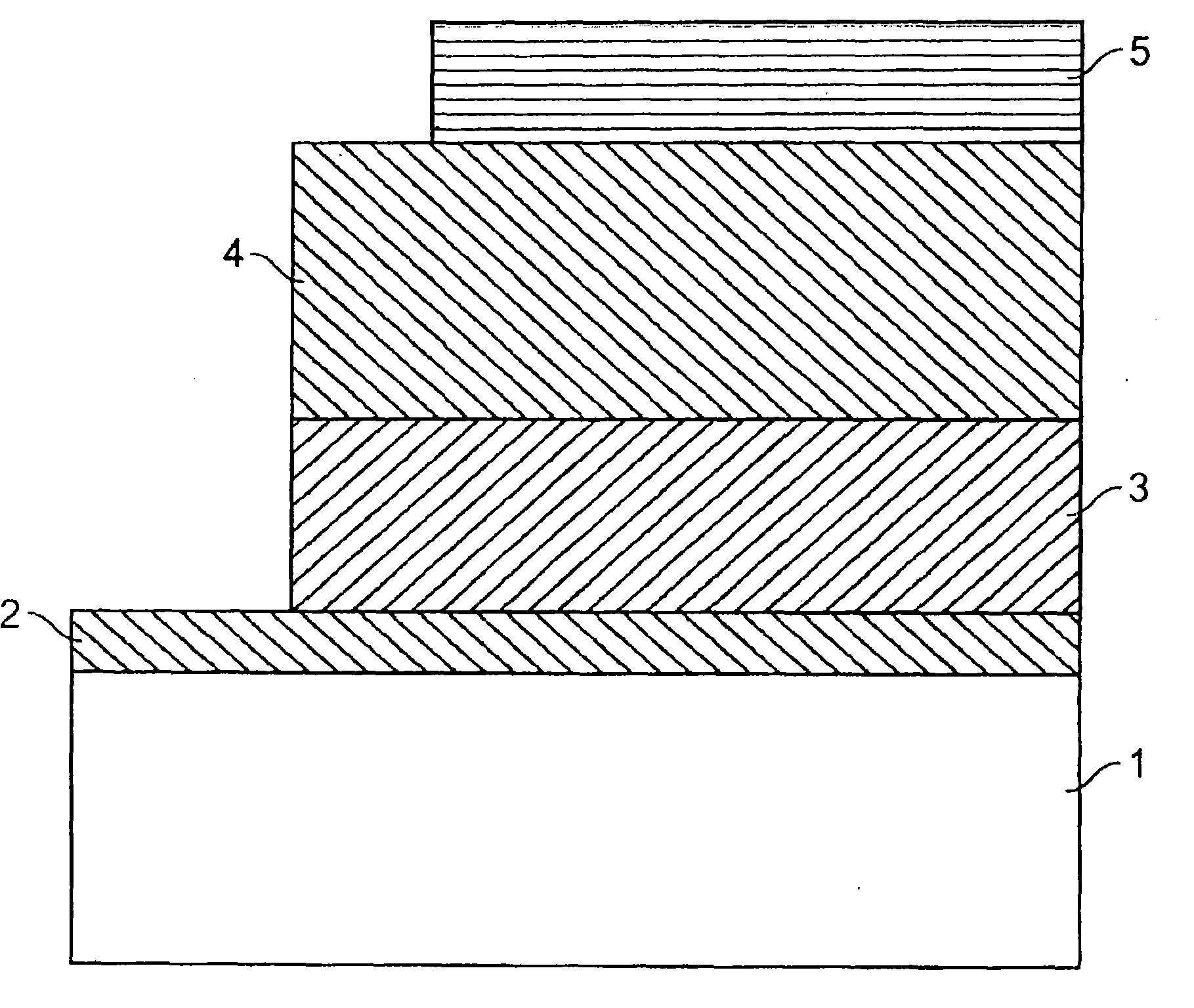
发光器件可具有如图1所示的结构,其中有第一电极2、与电极2相接触的第一层3、与层3相接触的第二层4、以及与第二层4相接触的第二电极5。第一层3和第二层4可各自为绝缘电介质。该结构的电极之一与衬底1相接触。各电极可与电源接触以跨越该结构提供电压。当跨越该异质结构施加适当极性的电压时,可通过该异质结构的发射层产生电致发光。可在该器件中,例如在第一层3与第二层4之间,包括单独的发射层(未示于图1中)。该单独的发射层可包含宽带隙材料。The light emitting device may have a structure as shown in FIG. 1, wherein there are a
衬底可为不透明或透明的。透明衬底可用于透明LED的制造。参见例如,Bulovic,V.等人的Nature 1996,380,29和Gu,G.等人的Appl.Phys.Lett.1996,68,2606-2608,其各自全部引入作为参考。透明LED可用于例如平视显示器,如在头盔护目镜或汽车挡风玻璃上的应用中。该衬底可为刚性或柔性的。该衬底可为塑料、金属或玻璃。第一电极可为例如高功函的空穴注入导体,如氧化铟锡(ITO)层。其它的第一电极材料可包括镓铟锡氧化物、锌铟锡氧化物、氮化钛或聚苯胺。第二电极可为例如低功函(例如,小于4.0eV)的电子注入金属,如Al、Ba、Yb、Ca、锂-铝合金(Li:Al)或镁-银合金(Mg:Ag)。第二电极如Mg:Ag可覆盖有不透明保护性金属层例如用于保护阴极层免受大气氧化的Ag层、或基本上透明ITO的相对薄的层。第一电极可具有约500


电介质层可包含根据其绝缘性能和与器件制造方法的相容性而选择的材料。一些示例性的电介质材料包括,但不限于,金属氧化物(例如氧化硅)和宽带隙聚合物(例如聚甲基丙烯酸甲酯)。发射层包含发射材料,优选具有宽带隙的发射材料。例如,硫化锌为合适的发射材料。The dielectric layer may comprise a material selected for its insulating properties and compatibility with device fabrication methods. Some exemplary dielectric materials include, but are not limited to, metal oxides (eg, silicon oxide) and wide bandgap polymers (eg, polymethyl methacrylate). The emissive layer contains an emissive material, preferably an emissive material with a wide bandgap. For example, zinc sulfide is a suitable emissive material.
在一些实施方式中,将电介质材料和发射材料组合在单一材料中。例如,可将硫化锌晶体涂覆或包封在电介质材料如聚合物中。这些聚合物涂覆的晶体可以单一材料同时起到电介质和发射材料的作用。In some embodiments, the dielectric material and emissive material are combined in a single material. For example, zinc sulfide crystals can be coated or encapsulated in a dielectric material such as a polymer. These polymer-coated crystals can function as both dielectric and emissive material in a single material.
这些层可通过旋涂、浸涂、蒸气沉积、溅射或其它薄膜沉积方法沉积在电极之一的表面上。第二电极可夹入、溅射到或蒸发到固体层的暴露表面上。可将电极之一或将两个电极都图案化。器件的电极可通过导电通路连接到电压源。在施加电压时,从该器件产生光。These layers can be deposited on the surface of one of the electrodes by spin coating, dip coating, vapor deposition, sputtering or other thin film deposition methods. The second electrode may be sandwiched, sputtered or evaporated onto the exposed surface of the solid layer. One of the electrodes or both electrodes can be patterned. The electrodes of the device can be connected to a voltage source through conductive paths. Upon application of a voltage, light is generated from the device.
有利地,无机半导体可在低温下例如通过溅射沉积在衬底上。通过跨越低压气体(例如氩气)施加高电压以产生高能态的电子和气体离子的等离子体而进行溅射。赋能等离子体离子撞击所需的涂覆材料的靶,导致原子从该靶以足够的能量射出而行进至衬底并与衬底结合。Advantageously, the inorganic semiconductor can be deposited on the substrate at low temperature, for example by sputtering. Sputtering is performed by applying a high voltage across a low pressure gas, such as argon, to create a plasma of electrons and gas ions in a high energy state. The energized plasma ions strike a target of the desired coating material, causing atoms to be ejected from the target with sufficient energy to travel to and bond with the substrate.
微接触印刷提供将材料施加到衬底上的预定区域上的方法。该预定区域是衬底上的其中材料被选择性地施加的区域。可对材料和衬底进行选择使得该材料基本上全部保持在预定区域中。通过选择形成图案的预定区域,可将材料施加到衬底上使得该材料形成图案。该图案可为规则图案(例如阵列、或系列线条)、或不规则图案。一旦衬底上形成材料图案,衬底可具有包含材料的区域(预定区域)和基本上不含有材料的区域。在一些情况中,材料在衬底上形成单层。预定区域可为不连续的区域。换言之,当将材料施加到衬底的预定区域上时,包含材料的位置可被基本上不含有材料的其它位置分开。在其它实例中,可通过喷墨印刷、旋涂、浸涂、微接触印刷或其它方法将半导体纳米晶体的多层沉积在表面上。该多层可为小于3μm厚、小于2μm厚、或小于1μm厚。Microcontact printing provides a method of applying materials to predetermined areas on a substrate. The predetermined area is the area on the substrate where material is selectively applied. The material and substrate can be selected such that substantially all of the material remains in the predetermined area. By selecting predetermined areas to be patterned, material can be applied to the substrate such that the material is patterned. The pattern can be a regular pattern, such as an array, or series of lines, or an irregular pattern. Once a pattern of material is formed on the substrate, the substrate may have regions containing material (predetermined regions) and regions substantially free of material. In some cases, the material forms a monolayer on the substrate. The predetermined area may be a discontinuous area. In other words, when material is applied to predetermined areas of the substrate, locations containing material may be separated by other locations substantially free of material. In other examples, multiple layers of semiconductor nanocrystals can be deposited on a surface by inkjet printing, spin coating, dip coating, microcontact printing, or other methods. The multiple layers may be less than 3 μm thick, less than 2 μm thick, or less than 1 μm thick.
通常,微接触印刷通过形成图案化的模具开始。该模具具有带有隆起和凹陷的图案的表面。例如,通过用在与图案化的模具表面接触的同时固化的液体聚合物前体涂覆模具的图案化表面,以隆起和凹陷的互补图案形成印模。随后可将印模上墨,即将印模与要沉积在衬底上的材料接触。该材料变得可逆地粘附到印模上。随后使上墨的印模与衬底接触。印模的隆起区域可接触衬底,同时印模的凹陷区域可与衬底分隔。在上墨的印模接触衬底之处,墨水材料(或其至少一部分)从印模转移到衬底上。这样,将隆起和凹陷的图案从印模转移至衬底作为衬底上包含材料和不含有材料的区域。微接触印刷和相关技术描述于例如美国专利No.5,512,131、6,180,239和6,518,168中,其各自全部引入作为参考。在一些情况中,印模可为具有墨水图案的无特征印模,其中该图案在将墨水施加到印模上时形成。参见2005年10月21日提交的美国专利申请No.11/253,612,其全部引入作为参考。Typically, microcontact printing begins by forming a patterned mold. The mold has a surface with a pattern of elevations and depressions. For example, a stamp is formed in a complementary pattern of elevations and depressions by coating the patterned surface of a mold with a liquid polymer precursor that solidifies while in contact with the patterned mold surface. The stamp can then be inked, ie the stamp is brought into contact with the material to be deposited on the substrate. The material becomes reversibly adhered to the impression. The inked stamp is then brought into contact with the substrate. The raised regions of the stamp may contact the substrate, while the recessed regions of the stamp may be spaced from the substrate. Where the inked stamp contacts the substrate, the ink material (or at least a portion thereof) is transferred from the stamp to the substrate. In this way, the pattern of elevations and depressions is transferred from the stamp to the substrate as material-containing and material-free regions on the substrate. Microcontact printing and related techniques are described, for example, in US Patent Nos. 5,512,131, 6,180,239, and 6,518,168, each of which is incorporated by reference in its entirety. In some cases, the stamp may be a featureless stamp with an ink pattern formed when the ink is applied to the stamp. See US Patent Application No. 11/253,612, filed October 21, 2005, which is incorporated by reference in its entirety.
图2描绘了概述微接触印刷过程中的基本步骤的流程图。首先,使用在硅表面上限定图案例如隆起和凹陷的图案的标准半导体加工技术制造硅母模(master)(或者,对于非图案化沉积,可使用空白Si母模)。然后将聚二甲基硅氧烷(PDMS,例如Sylgard 184)前体混合,脱气,倾倒到该母模上,和再次脱气,并且容许其在室温下(或者为了更快的固化时间,高于室温)固化(步骤1)。然后使具有包含硅母模图案的表面的PDMS脱离母模,并将其切割为所需形状和尺寸。然后用选择以如需要地容易地粘附和释放墨水的表面化学层覆盖该印模。例如,该表面化学层可为化学气相沉积的聚对亚苯基二甲基-C层。取决于要复制的图案,该表面化学层可为例如0.1至2μm厚(步骤2)。然后例如通过旋转流延、注射泵分配、或喷墨印刷半导体纳米晶体溶液而将印模上墨(步骤3)。该溶液可具有例如在氯仿中1至10mg/mL的浓度。该浓度可根据所需结果而改变。然后可将上墨的印模与衬底接触,并且施加轻微的压力例如30秒以将墨水(即半导体纳米晶体单层)完全转移到该新的衬底上(步骤4)。图2A和2B描绘ITO涂覆的玻璃衬底的制备。将第一层如第一电介质层沉积到ITO衬底上。将图案化的半导体纳米晶体单层转移到该层上,然后可添加该器件的剩余部分(步骤5)。参见,例如,均在2005年10月21日提交的美国专利申请No.11/253,595和11/253,612以及2005年1月11日提交的美国专利申请No.11/032,163,其各自引入本文作为参考。Figure 2 depicts a flowchart outlining the basic steps in the microcontact printing process. First, a silicon master (alternatively, for non-patterned deposition, a blank Si master can be used) is fabricated using standard semiconductor processing techniques that define a pattern, such as a pattern of bumps and depressions, on a silicon surface. The polydimethylsiloxane (PDMS, such as Sylgard 184) precursor is then mixed, degassed, poured onto the master, and degassed again, and allowed to cool at room temperature (or for faster cure times, above room temperature) to cure (step 1). The PDMS with a surface containing the silicon master pattern is then detached from the master and cut to the desired shape and size. The stamp is then covered with a surface chemistry layer selected to readily adhere and release ink as desired. For example, the surface chemical layer may be a chemical vapor deposited parylene-C layer. Depending on the pattern to be replicated, this surface chemical layer may be eg 0.1 to 2 μm thick (step 2). The stamp is then inked (step 3), for example by spin casting, syringe pump dispensing, or inkjet printing of the semiconductor nanocrystal solution. The solution may have, for example, a concentration of 1 to 10 mg/mL in chloroform. The concentration can be varied according to the desired result. The inked stamp can then be brought into contact with the substrate, and light pressure applied, eg, for 30 seconds, to completely transfer the ink (ie semiconductor nanocrystal monolayer) to the new substrate (step 4). 2A and 2B depict the preparation of ITO-coated glass substrates. A first layer, such as a first dielectric layer, is deposited onto the ITO substrate. A patterned monolayer of semiconductor nanocrystals is transferred onto this layer, and then the remainder of the device can be added (step 5). See, e.g., U.S. Patent Application Nos. 11/253,595 and 11/253,612, both filed October 21, 2005, and U.S. Patent Application No. 11/032,163, filed January 11, 2005, each of which is incorporated herein by reference .
可与器件结构组合选择器件材料的电性能(如带隙和能带偏移)以制造其中激子基本上在宽带隙发射材料上形成的器件。该发射材料可在光从该器件发射之前将能量转移至发射-变换(emission-altering)材料。能量转移可通过光从发射材料的发射和被发射-变换材料的再吸收而发生。或者,能量转移可为具有光发射和再吸收的能量的转移(如

半导体纳米晶体可有利地用作发射-变换材料。半导体纳米晶体可具有带有强烈的窄带发射的宽吸收带。取决于纳米晶体的尺寸、形状、组成和结构构造,发射的峰值波长可在整个可见和红外区域内调节。纳米晶体可备有具有所需化学特性(例如所需溶解度)的外表面。通过纳米晶体的光发射可为长期稳定的。Semiconductor nanocrystals can advantageously be used as emission-converting materials. Semiconductor nanocrystals can have broad absorption bands with strong narrowband emissions. Depending on the size, shape, composition, and structural configuration of the nanocrystals, the peak wavelength of emission can be tuned throughout the visible and infrared regions. Nanocrystals can be provided with outer surfaces having desired chemical properties, such as desired solubility. Light emission by nanocrystals can be long-term stable.
当纳米晶体达到激发态(或者换言之,激子位于纳米晶体上)时,可在发射波长处发生发射。该发射具有相应于量子限制的半导体材料的带隙的频率。该带隙是纳米晶体尺寸的函数。具有小直径的纳米晶体可具有介于物质的分子和大块(bulk)形式之间的性质。例如,具有小直径的基于半导体材料的纳米晶体可表现出在所有三维中电子和空穴两者的量子限制,这导致随着微晶尺寸减小材料的有效带隙增加。因此,随着微晶尺寸减小,纳米晶体的光学吸收和发射两者蓝移,或者向较高的能量移动。When the nanocrystal reaches an excited state (or in other words, excitons are located on the nanocrystal), emission can occur at the emission wavelength. This emission has a frequency corresponding to the bandgap of the quantum confined semiconductor material. This bandgap is a function of nanocrystal size. Nanocrystals with small diameters can have properties intermediate between molecular and bulk forms of matter. For example, nanocrystals based on semiconductor materials with small diameters can exhibit quantum confinement of both electrons and holes in all three dimensions, which leads to an increase in the effective bandgap of the material as the crystallite size decreases. Thus, as the crystallite size decreases, both the optical absorption and emission of the nanocrystals blue shift, or shift toward higher energies.
来自纳米晶体的发射可为窄的高斯发射带,其可通过改变纳米晶体的尺寸、纳米晶体的组成、或者这两者而在光谱的紫外、可见或红外区域的整个完整波长范围内进行调节。例如,CdSe可在可见区域内调节并且InAs可在红外区域内调节。纳米晶体群的窄尺寸分布可导致在窄的光谱范围内的光发射。所述群可为单分散的并且可在纳米晶体直径上呈现出小于15%rms的偏差,优选小于10%,更优选小于5%。可观察到纳米晶体在可见区域内发射的在不大于约75nm,优选60nm,更优选40nm,且最优选30nm半宽度(FWHM)的窄范围内的光谱发射。IR-发射的纳米晶体可具有不大于150nm,或者不大于100nm的FWHM。以发射能量表示,该发射可具有不大于0.05eV或不大于0.03eV的FWHM。发射宽度随着纳米晶体直径分散性的减小而减小。半导体纳米晶体可具有高的发射量子效率如大于10%、20%、30%、40%、50%、60%、70%或80%。Emission from the nanocrystals can be a narrow Gaussian emission band that can be tuned across the full wavelength range of the ultraviolet, visible, or infrared region of the spectrum by varying the size of the nanocrystal, the composition of the nanocrystal, or both. For example, CdSe is tunable in the visible region and InAs is tunable in the infrared region. The narrow size distribution of the nanocrystal population can result in light emission in a narrow spectral range. The population may be monodisperse and may exhibit less than 15% rms variation in nanocrystal diameter, preferably less than 10%, more preferably less than 5%. The spectral emission emitted by the nanocrystals in the visible region can be observed within a narrow range of no greater than about 75 nm, preferably 60 nm, more preferably 40 nm, and most preferably 30 nm full width at half width (FWHM). The IR-emitting nanocrystals may have a FWHM of no greater than 150 nm, or no greater than 100 nm. Expressed in terms of emission energy, the emission may have a FWHM of not greater than 0.05 eV or not greater than 0.03 eV. The emission width decreases with decreasing nanocrystal diameter dispersion. Semiconductor nanocrystals may have high emission quantum efficiencies such as greater than 10%, 20%, 30%, 40%, 50%, 60%, 70%, or 80%.
形成纳米晶体的半导体可包括II-VI族化合物、II-V族化合物、III-VI族化合物、III-V族化合物、IV-VI族化合物、I-III-VI族化合物、II-IV-VI族化合物或II-IV-V族化合物,例如,ZnO、ZnS、ZnSe、ZnTe、CdO、CdS、CdSe、CdTe、MgO、MgS、MgSe、MgTe、HgO、HgS、HgSe、HgTe、AlN、AlP、AlAs、AlSb、GaN、GaP、GaAs、GaSb、InN、InP、InAs、InSb、TlN、TlP、TlAs、TlSb、TlSb、PbS、PbSe、PbTe、或其混合物。Nanocrystal-forming semiconductors may include II-VI compounds, II-V compounds, III-VI compounds, III-V compounds, IV-VI compounds, I-III-VI compounds, II-IV-VI Group II-IV-V compounds, such as ZnO, ZnS, ZnSe, ZnTe, CdO, CdS, CdSe, CdTe, MgO, MgS, MgSe, MgTe, HgO, HgS, HgSe, HgTe, AlN, AlP, AlAs , AlSb, GaN, GaP, GaAs, GaSb, InN, InP, InAs, InSb, TlN, TlP, TlAs, TlSb, TlSb, PbS, PbSe, PbTe, or mixtures thereof.
制备单分散半导体纳米晶体的方法包括注入到热的配位溶剂中的有机金属试剂如二甲基镉的热解。这允许离散成核并导致宏观量的纳米晶体的受控生长。纳米晶体的制备和处理描述于例如美国专利6,322,901和6,576,291以及美国专利申请No.60/550,314中,其各自全部引入作为参考。制造纳米晶体的方法是胶体生长法。胶体生长通过将M给体和X给体快速注射到热的配位溶剂中而发生。该注射产生核,其可以受控方式生长以形成纳米晶体。该反应混合物可温和加热以生长纳米晶体并使纳米晶体退火。样品中纳米晶体的平均尺寸和尺寸分布均依赖于生长温度。维持稳定的生长所必需的生长温度随着平均晶体尺寸的增大而提高。纳米晶体是纳米晶体群的一员。由于离散成核和受控生长,所获得的纳米晶体群具有窄的单分散的直径分布。单分散的直径分布也可称为尺寸。成核后在配位溶剂中纳米晶体的受控生长和退火也可导致均匀的表面衍生和规则的核结构。随着尺寸分布锐化,可升温以维持稳定的生长。通过添加更多M给体或X给体,可缩短生长期。A method of preparing monodisperse semiconductor nanocrystals involves the pyrolysis of an organometallic reagent such as dimethylcadmium injected into a hot coordinating solvent. This allows discrete nucleation and leads to the controlled growth of macroscopic quantities of nanocrystals. The preparation and processing of nanocrystals is described, for example, in US Patents 6,322,901 and 6,576,291 and US Patent Application No. 60/550,314, each of which is incorporated by reference in its entirety. The method of making nanocrystals is the colloidal growth method. Colloidal growth occurs by rapid injection of M and X donors into a hot coordinating solvent. This injection produces nuclei that can grow in a controlled manner to form nanocrystals. The reaction mixture can be heated gently to grow and anneal the nanocrystals. Both the average size and the size distribution of nanocrystals in a sample depend on the growth temperature. The growth temperature necessary to maintain stable growth increases with increasing average crystal size. Nanocrystals are members of the group of nanocrystals. Due to discrete nucleation and controlled growth, the obtained population of nanocrystals has a narrow monodisperse diameter distribution. A monodisperse diameter distribution may also be referred to as size. Controlled growth and annealing of nanocrystals in coordinating solvents after nucleation can also lead to uniform surface derivatization and regular core structures. As the size distribution sharpens, the temperature can be raised to maintain steady growth. The growth phase can be shortened by adding more M donor or X donor.
M给体可为无机化合物、有机金属化合物或元素金属。M为镉、锌、镁、汞、铝、镓、铟或铊。X给体为能够与M给体反应形成具有通式MX的材料的化合物。典型地,X给体为硫属化物给体或磷属元素化物给体,如膦硫属化物、双(甲硅烷基)硫属化物、二氧、铵盐、或三(甲硅烷基)磷属元素化物。合适的X给体包括二氧、双(三甲基甲硅烷基)硒化物((TMS)2Se)、三烷基膦硒化物如(三正辛基膦)硒化物(TOPSe)或(三正丁基膦)硒化物(TBPSe)、三烷基膦碲化物如(三正辛基膦)碲化物(TOPTe)或六丙基磷三酰胺碲化物(HPPTTe)、双(三甲基甲硅烷基)碲化物((TMS)2Te)、双(三甲基甲硅烷基)硫化物((TMS)2S)、三烷基膦硫化物如(三正辛基膦)硫化物(TOPS)、铵盐如卤化铵(例如NH4Cl)、三(三甲基甲硅烷基)磷化物((TMS)3P)、三(三甲基甲硅烷基)砷化物((TMS)3As)、或三(三甲基甲硅烷基)锑化物((TMS)3Sb)。在一些实施方式中,M给体和X给体可为在相同分子内的部分。The M donor can be an inorganic compound, an organometallic compound, or an elemental metal. M is cadmium, zinc, magnesium, mercury, aluminum, gallium, indium or thallium. The X donor is a compound capable of reacting with the M donor to form a material having the general formula MX. Typically, the X donor is a chalcogenide donor or a pnictide donor, such as a phosphine chalcogenide, bis(silyl)chalcogenide, dioxo, ammonium salt, or tris(silyl)phosphorus Elemental compounds. Suitable X donors include dioxygen, bis(trimethylsilyl)selenide ((TMS) 2Se ), trialkylphosphineselenides such as (tri-n-octylphosphine)selenide (TOPSe) or (tris-n-octylphosphine)selenide (TOPSe) n-butylphosphine) selenide (TBPSe), trialkylphosphine telluride such as (tri-n-octylphosphine) telluride (TOPTe) or hexapropylphosphorustriamide telluride (HPPTTe), bis(trimethylsilyl base) tellurides ((TMS) 2 Te), bis(trimethylsilyl) sulfides ((TMS) 2 S), trialkylphosphine sulfides such as (tri-n-octylphosphine) sulfide (TOPS) , ammonium salts such as ammonium halides (e.g. NH 4 Cl), tris(trimethylsilyl)phosphide ((TMS) 3 P), tris(trimethylsilyl)arsenide ((TMS) 3 As) , or tris(trimethylsilyl)antimonide ((TMS) 3 Sb). In some embodiments, the M donor and the X donor can be moieties within the same molecule.
配位溶剂可帮助控制纳米晶体的生长。配位溶剂为具有给体孤对的化合物,例如,具有可用于配位到生长纳米晶体表面的孤电子对的化合物。溶剂配位可使生长纳米晶体稳定化。典型的配位溶剂包括烷基膦、烷基膦氧化物、烷基膦酸或烷基次膦酸,然而,其它配位溶剂如吡啶、呋喃和胺也可适于纳米晶体生产。合适的配位溶剂的例子包括吡啶、三正辛基膦(TOP)、氧化三正辛基膦(TOPO)和三羟丙基膦(tHPP)。可使用工业级TOPO。Coordinating solvents can help control the growth of nanocrystals. A coordinating solvent is a compound with a lone pair of donors, eg, a compound with a lone pair of electrons available for coordination to the surface of a growing nanocrystal. Solvent coordination can stabilize the growing nanocrystals. Typical coordinating solvents include alkylphosphines, alkylphosphine oxides, alkylphosphonic acids, or alkylphosphinic acids, however, other coordinating solvents such as pyridine, furan, and amines may also be suitable for nanocrystal production. Examples of suitable coordinating solvents include pyridine, tri-n-octylphosphine (TOP), tri-n-octylphosphine oxide (TOPO) and trihydroxypropylphosphine (tHPP). Industrial grade TOPO can be used.
在反应的生长阶段期间的尺寸分布可通过监控颗粒的吸收线宽来评估。响应于颗粒的吸收光谱中的变化调整反应温度容许在生长期间维持尖锐的粒度分布。可在晶体生长期间将反应物添加到成核溶液中以生长更大的晶体。通过在特定纳米晶体平均直径处停止生长和选择半导体材料的合适组成,对于CdSe和CdTe,可在300nm至5μm、或300nm至800nm的波长范围内连续地调节纳米晶体的发射光谱。纳米晶体具有小于150的直径。纳米晶体群具有在15

纳米晶体可为具有窄尺寸分布的纳米晶体群中的一员。纳米晶体可为球、棒、盘或其它形状。纳米晶体可包括半导体材料核。纳米晶体可包括具有式MX的核,其中M为镉、锌、镁、汞、铝、镓、铟、铊、或其混合物,和X为氧、硫、硒、碲、氮、磷、砷、锑、或其混合物。A nanocrystal can be a member of a population of nanocrystals with a narrow size distribution. Nanocrystals can be spheres, rods, disks or other shapes. Nanocrystals may include a core of semiconductor material. Nanocrystals can include a core having the formula MX, where M is cadmium, zinc, magnesium, mercury, aluminum, gallium, indium, thallium, or mixtures thereof, and X is oxygen, sulfur, selenium, tellurium, nitrogen, phosphorus, arsenic, Antimony, or mixtures thereof.
所述核可在该核的表面上具有外覆层(overcoating)。外覆层可为具有与核的组成不同的组成的半导体材料。纳米晶体表面上的半导体材料外覆层可包括II-VI族化合物、II-V族化合物、III-VI族化合物、III-V族化合物、IV-VI族化合物、I-III-VI族化合物、II-IV-VI族化合物和II-IV-V族化合物,例如,ZnO、ZnS、ZnSe、ZnTe、CdO、CdS、CdSe、CdTe、MgO、MgS、MgSe、MgTe、HgO、HgS、HgSe、HgTe、AlN、AlP、AlAs、AlSb、GaN、GaP、GaAs、GaSb、InN、InP、InAs、InSb、TlN、TlP、TlAs、TlSb、TlSb、PbS、PbSe、PbTe、或其混合物。例如,ZnS、ZnSe或CdS外覆层可在CdSe或CdTe纳米晶体上生长。外覆方法描述于例如美国专利6,322,901中。通过调节在外覆过程中反应混合物的温度和监控核的吸收光谱,可获得具有高的发射量子效率和窄的尺寸分布的外覆材料。外覆层可为1至10个单层厚。The core may have an overcoating on the surface of the core. The cladding layer may be a semiconductor material having a composition different from that of the core. The semiconductor material coating layer on the surface of the nanocrystal can include II-VI group compound, II-V group compound, III-VI group compound, III-V group compound, IV-VI group compound, I-III-VI group compound, II-IV-VI compounds and II-IV-V compounds, for example, ZnO, ZnS, ZnSe, ZnTe, CdO, CdS, CdSe, CdTe, MgO, MgS, MgSe, MgTe, HgO, HgS, HgSe, HgTe, AlN, AlP, AlAs, AlSb, GaN, GaP, GaAs, GaSb, InN, InP, InAs, InSb, TlN, TlP, TlAs, TlSb, TlSb, PbS, PbSe, PbTe, or mixtures thereof. For example, a ZnS, ZnSe or CdS overcoat can be grown on CdSe or CdTe nanocrystals. Overcoating methods are described, for example, in US Patent 6,322,901. By adjusting the temperature of the reaction mixture and monitoring the absorption spectrum of the core during the coating process, coating materials with high emission quantum efficiency and narrow size distribution can be obtained. The outer covering may be 1 to 10 monolayers thick.
粒度分布可如美国专利6,322,901中所述,通过以纳米晶体的不良溶剂如甲醇/丁醇进行尺寸选择性沉淀而进一步精制。例如,可将纳米晶体分散于丁醇在己烷中的10%的溶液中。可将甲醇滴加到该搅拌着的溶液中直至乳白色持续。由离心导致的上清液和絮凝物的分离产生富集有样品中的最大微晶的沉淀物。可重复该步骤直至注意到没有光吸收光谱的进一步锐化。尺寸选择性沉淀可在多种溶剂/非溶剂对中进行,包括吡啶/己烷和氯仿/甲醇。经尺寸选择的纳米晶体群可具有距平均直径不大于15%rms的偏差,优选10%rms的偏差或更小,并且更优选5%rms的偏差或更小。The particle size distribution can be further refined by size selective precipitation with a poor solvent for the nanocrystals, such as methanol/butanol, as described in US Patent 6,322,901. For example, nanocrystals can be dispersed in a 10% solution of butanol in hexane. Methanol can be added dropwise to the stirring solution until the milky color persists. Separation of supernatant and flocs by centrifugation produces a precipitate enriched with the largest crystallites in the sample. This step can be repeated until no further sharpening of the light absorption spectrum is noted. Size-selective precipitation can be performed in a variety of solvent/non-solvent pairs, including pyridine/hexane and chloroform/methanol. The size-selected population of nanocrystals may have a deviation of no more than 15% rms from the mean diameter, preferably a deviation of 10% rms or less, and more preferably a deviation of 5% rms or less.
纳米晶体的外表面可包括得自在生长期间所使用的配位溶剂的化合物。该表面可通过重复暴露于过量的竞争配位基团进行改性。例如,被覆盖的纳米晶体的分散体可用配位有机化合物如吡啶处理,以产生容易地分散在吡啶、甲醇和芳香族化合物中但不再分散在脂肪族溶剂中的微晶。这种表面交换过程可用任何能够与纳米晶体的外表面配位或结合的化合物进行,包括例如膦、硫醇、胺和磷酸酯(盐)。可将纳米晶体暴露于短链聚合物,其呈现出对该表面的亲和性和以对悬浮或分散介质具有亲和性的部分封端。这种亲和性改善该悬浮体的稳定性并阻碍纳米晶体的絮凝。纳米晶体配位化合物描述于例如美国专利No.6,251,303中,该专利全部引入作为参考。The outer surface of the nanocrystals may include compounds derived from the coordinating solvent used during growth. This surface can be modified by repeated exposure to excess competing coordinating groups. For example, dispersions of capped nanocrystals can be treated with coordinating organic compounds such as pyridine to produce crystallites that are readily dispersed in pyridine, methanol, and aromatic compounds but no longer disperse in aliphatic solvents. This surface exchange process can be performed with any compound capable of coordinating or binding to the outer surface of the nanocrystal, including, for example, phosphines, thiols, amines, and phosphates. Nanocrystals can be exposed to short-chain polymers that exhibit an affinity for the surface and end caps with moieties that have an affinity for the suspension or dispersion medium. This affinity improves the stability of the suspension and hinders the flocculation of the nanocrystals. Nanocrystalline coordination compounds are described, for example, in US Patent No. 6,251,303, which is incorporated by reference in its entirety.
更具体地,配位配体可具有下式:More specifically, a coordinating ligand can have the formula:

其中k为2、3或5,并且n为1、2、3、4或5,使得k-n不小于0;X为O、S、S=O、SO2、Se、Se=O、N、N=O、P、P=O、As、或As=O;Y和L各自独立地为芳基,杂芳基,或任选地含有至少一个双键、至少一个三键、或至少一个双键及一个三键的直链或支链C2-12烃链。该烃链可任选地被一个或多个C1-4烷基、C2-4烯基、C2-4炔基、C1-4烷氧基、羟基、卤素、氨基、硝基、氰基、C3-5环烷基、3-5元杂环烷基、芳基、杂芳基、C1-4烷羰氧基、C1-4烷氧羰基、C1-4烷羰基或甲酰基。该烃链还可任选地被-O-、-S-、-N(Ra)-、-N(Ra)-C(O)-O-、-O-C(O)-N(Ra)-、-N(Ra)-C(O)-N(Rb)-、-O-C(O)-O-、-P(Ra)-或-P(O)(Ra)-中断。Ra和Rb各自独立地为氢、烷基、烯基、炔基、烷氧基、羟烷基、羟基或卤代烷基。Where k is 2, 3 or 5, and n is 1, 2, 3, 4 or 5, so that kn is not less than 0; X is O, S, S=O, SO 2 , Se, Se=O, N, N =O, P, P=O, As, or As=O; Y and L are each independently aryl, heteroaryl, or optionally contain at least one double bond, at least one triple bond, or at least one double bond And a straight or branched C2-12 hydrocarbon chain with a triple bond. The hydrocarbon chain can optionally be replaced by one or more C 1-4 alkyl, C 2-4 alkenyl, C 2-4 alkynyl, C 1-4 alkoxy, hydroxyl, halogen, amino, nitro, Cyano, C 3-5 cycloalkyl, 3-5 membered heterocycloalkyl, aryl, heteroaryl, C 1-4 alkoxycarbonyl, C 1-4 alkoxycarbonyl, C 1-4 alkoxycarbonyl or formyl. The hydrocarbon chain can optionally be replaced by -O-, -S-, -N(R a )-, -N(R a )-C(O)-O-, -OC(O)-N(R a )-, -N(R a )-C(O)-N(R b )-, -OC(O)-O-, -P(R a )- or -P(O)(R a )-interruption . R a and R b are each independently hydrogen, alkyl, alkenyl, alkynyl, alkoxy, hydroxyalkyl, hydroxy, or haloalkyl.
芳基为取代或未取代的环状芳族基团。实例包括苯基、苄基、萘基、甲苯基、蒽基、硝基苯基或卤代苯基。杂芳基为在环中具有一个或多个杂原子的芳基,例如呋喃基、吡啶基、吡咯基或菲基。Aryl is a substituted or unsubstituted cyclic aromatic group. Examples include phenyl, benzyl, naphthyl, tolyl, anthracenyl, nitrophenyl or halophenyl. Heteroaryl is an aryl group having one or more heteroatoms in the ring, such as furyl, pyridyl, pyrrolyl or phenanthrenyl.
合适的配位配体可商购或通过普通有机合成技术例如如J.March,Advanced OrganicChemistry中所述制备,该文献全部引入作为参考。Suitable coordinating ligands are commercially available or can be prepared by common organic synthesis techniques, eg as described in J. March, Advanced Organic Chemistry , which is incorporated by reference in its entirety.
透射电子显微术(TEM)可提供关于纳米晶体群的尺寸、形状和分布的信息。粉末X射线衍射(XRD)图样可提供关于纳米晶体的晶体结构的类型和质量的最完整信息。尺寸的估算也是可能的,因为粒径经由X-射线相干长度与峰宽成反比。例如,纳米晶体的直径可通过透射电子显微术直接测量或利用例如Scherrer方程由X-射线衍射数据估算。其还可由UV/Vis吸收光谱估算。Transmission electron microscopy (TEM) can provide information on the size, shape and distribution of nanocrystal populations. Powder X-ray Diffraction (XRD) patterns can provide the most complete information on the type and quality of the crystal structure of the nanocrystals. Estimation of size is also possible because particle size is inversely proportional to peak width via X-ray coherence length. For example, the diameter of a nanocrystal can be measured directly by transmission electron microscopy or estimated from X-ray diffraction data using, for example, the Scherrer equation. It can also be estimated from UV/Vis absorption spectroscopy.
单独的器件可形成于单一衬底上的多个位置处以形成显示器。该显示器可包括以不同波长发射的器件。通过将具有发射不同颜色的材料阵列的衬底图案化,可形成包括不同颜色的像素的显示器。在一些应用中,该衬底可包括后板(backplane)。后板包括用于控制或转换对单独像素的功率的有源(active)或无源(passive)电子设备。包括后板对于如显示器、传感器或成像器的应用可为有用的。特别地,后板可构造作为有源矩阵、无源矩阵、固定格式、直接驱动或混合型。显示器可构造用于静置图像、活动图像、或照明。照明显示器可提供白光、单色光、或颜色可调的光。参见例如2005年10月21日提交的美国专利申请No.11/253,612,其全部引入作为参考。Individual devices can be formed at multiple locations on a single substrate to form a display. The display may include devices emitting at different wavelengths. By patterning a substrate with an array of materials that emit different colors, a display can be formed that includes pixels of different colors. In some applications, the substrate can include a backplane. The backplane includes active or passive electronics for controlling or switching power to individual pixels. Including a backplane may be useful for applications such as displays, sensors or imagers. In particular, the backplane can be configured as active matrix, passive matrix, fixed format, direct drive or hybrid. Displays can be configured for still images, moving images, or illumination. Illuminated displays can provide white light, monochromatic light, or color-tunable light. See, eg, US Patent Application No. 11/253,612, filed October 21, 2005, which is incorporated by reference in its entirety.
所述器件可在受控(无氧和无水分)环境中制造,防止在制造过程期间的发光效率的弱化(quenching)。其它多层结构可用于改善器件性能(参见例如,The devices can be fabricated in a controlled (oxygen and moisture free) environment, preventing quenching of luminous efficiency during the fabrication process. Other multilayer structures can be used to improve device performance (see, e.g.,
发光器件的性能可通过提高它们的效率、使它们的发射光谱变窄或变宽、或使它们的发射偏振而改善。参见例如,Bulovic等的Semiconductors andSemimetals 64,255(2000)、Adachi等的Appl.Phys.Lett.78,1622(2001)、Yamasaki等的Appl.Phys.Lett.76,1243(2000)、Dirr等的Jpn.J.Appl.Phys.37,1457(1998)和D’Andrade等的MRS Fall Meeting,BB6.2(2001),这些文献中的每一篇均全部引入本文作为参考。纳米晶体可包含在有效的混合型有机/无机发光器件中。The performance of light emitting devices can be improved by increasing their efficiency, narrowing or broadening their emission spectra, or polarizing their emission. See, for example, Semiconductors and Semimetals 64, 255 (2000) of Bulovic et al., Appl. Phys. Lett. 78, 1622 (2001) of Adachi et al., Appl. Phys. Lett. Jpn. J. Appl. Phys. 37, 1457 (1998) and D'Andrade et al. MRS Fall Meeting, BB6.2 (2001), each of which is incorporated herein by reference in its entirety. Nanocrystals can be incorporated into efficient hybrid organic/inorganic light-emitting devices.
纳米晶体的窄FWHM可导致饱和的颜色发射。这可导致即使在可见光谱的红色和蓝色部分也为有效的纳米晶体发光器件,因为在纳米晶体发射器件中,对于红外和紫外发射没有损失光子。在单一材料体系的整个可见光谱范围内的可广泛调节的饱和的颜色发射是任何种类的有机发色团都不匹配的(参见例如Dabbousi等的J.Phys.Chem.101,9463(1997),其全部引入作为参考)。单分散的纳米晶体群将发射跨越窄波长范围的光。包含多于一种尺寸的纳米晶体的器件可发射多于一种窄波长范围的光。由观察者感知到的所发射的光的颜色可通过选择器件中的纳米晶体尺寸和材料适当组合进行控制。纳米晶体的带边能级的简并促进所有可能的激子的俘获和辐射复合,不管这些激子是由直接的电荷注入、能量转移还是光的吸收而产生的。The narrow FWHM of nanocrystals can lead to saturated color emission. This can lead to nanocrystal light emitting devices that are efficient even in the red and blue parts of the visible spectrum, since in nanocrystal emitting devices no photons are lost for infrared and ultraviolet emission. Broadly tunable saturated color emission over the entire visible spectral range of a single material system is unmatched by any kind of organic chromophore (see e.g. J. Phys. Chem. 101, 9463 (1997) by Dabbousi et al. It is incorporated by reference in its entirety). A monodisperse population of nanocrystals will emit light spanning a narrow wavelength range. Devices comprising nanocrystals of more than one size can emit light in more than one narrow wavelength range. The color of the emitted light perceived by the observer can be controlled by selecting the appropriate combination of nanocrystal size and materials in the device. The degeneracy of the band-edge energy levels of nanocrystals facilitates the trapping and radiative recombination of all possible excitons, whether generated by direct charge injection, energy transfer, or light absorption.
可制备发射可见或红外光的器件。可选择半导体纳米晶体的尺寸和材料,使得纳米晶体发射选定波长的可见或红外光。该波长可为300至2,500nm或更大,例如300至400nm、400至700nm、700至1100nm、1100至2500nm、或大于2500nm。Devices that emit visible or infrared light can be fabricated. The size and material of the semiconductor nanocrystals can be selected such that the nanocrystals emit visible or infrared light at selected wavelengths. The wavelength may be from 300 to 2,500 nm or greater, such as 300 to 400 nm, 400 to 700 nm, 700 to 1100 nm, 1100 to 2500 nm, or greater than 2500 nm.
单独的器件可形成于单一衬底上的多个位置处以形成显示器。该显示器可包括以不同波长进行发射的器件。通过将具有发射不同颜色的半导体纳米晶体阵列的衬底图案化,可形成包括不同颜色的像素的显示器。Individual devices can be formed at multiple locations on a single substrate to form a display. The display may include devices that emit at different wavelengths. By patterning a substrate with an array of semiconductor nanocrystals emitting different colors, a display can be formed that includes pixels of different colors.
图3A说明电压驱动的电致发光器件的横截面图。在该器件中,半导体纳米晶体层003(其可为半导体纳米晶体的部分单层、单层、或多层)和宽带隙材料层004堆叠在衬底007上的两个绝缘层002、005与两个导电电极001、006之间。保护层000、导电层001和绝缘层002是透明的以容许在宽带隙材料层004和半导体纳米晶体层003中产生的光射出该器件。或者,光可射出衬底侧,条件是底电极和衬底是透明的。Figure 3A illustrates a cross-sectional view of a voltage driven electroluminescent device. In this device, a semiconductor nanocrystal layer 003 (which may be part of a single layer, a single layer, or multiple layers of a semiconductor nanocrystal) and a wide bandgap material layer 004 are stacked on a substrate 007 with two insulating layers 002, 005 and Between two conductive electrodes 001, 006. The
根据该构造,电压驱动的纳米晶体电致发光器件在两个绝缘层与导电电极之间包括含有纳米晶体和宽带隙材料(如硫化锌)的光发射层。跨越两个导电电极施加电压以电驱动和激发宽带隙材料;激发能量通过发射光子或通过转移能量至纳米晶体层而释放。因而,纳米晶体层起到将电能直接或间接地转换为光子能的能量转换层的作用。作为在纳米晶体层内的能量转换的结果,与纳米晶体的能量结构有关的光被发射。因此,可设计纳米晶体的尺寸或组成以获得红、绿或蓝色、或颜色组合的光发射,并仍然保持宽带隙材料的化学组成不变。According to this configuration, a voltage-driven nanocrystal electroluminescent device includes a light-emitting layer comprising nanocrystals and a wide bandgap material such as zinc sulfide between two insulating layers and a conductive electrode. A voltage is applied across two conductive electrodes to electrically drive and excite the wide bandgap material; the excitation energy is released by emitting photons or by transferring energy to the nanocrystal layer. Thus, the nanocrystal layer functions as an energy conversion layer that directly or indirectly converts electrical energy into photon energy. As a result of energy conversion within the nanocrystal layer, light associated with the energy structure of the nanocrystal is emitted. Thus, the size or composition of the nanocrystals can be engineered for red, green, or blue light emission, or a combination of colors, and still keep the chemical composition of the wide bandgap material constant.
图3B显示电压驱动的纳米晶体电致发光器件的替换构造。这里,半导体纳米晶体103分散在衬底107上两个绝缘层102、105与两个导电电极101、106之间的宽带隙材料104基质中。来自混合的纳米晶体层和宽带隙材料层的光从顶部和/或底部射出。Figure 3B shows an alternative configuration of a voltage-driven nanocrystal electroluminescent device. Here, semiconductor nanocrystals 103 are dispersed in a matrix of wide bandgap material 104 between two insulating layers 102 , 105 and two conductive electrodes 101 , 106 on a substrate 107 . Light from the mixed nanocrystal layer and wide bandgap material layer emerges from the top and/or bottom.
图3C显示电压驱动的纳米晶体电致发光器件的替换构造。这里,半导体纳米晶体201位于在顶电极202、电介质203、宽带隙材料204、电介质205、电极206和衬底207之外的区域中。纳米晶体201可任选地被覆盖层200(不一定存在)保护。来自宽带隙材料层的光可通过能量转移或再吸收而激发纳米晶体。Figure 3C shows an alternative configuration of a voltage-driven nanocrystal electroluminescent device. Here, semiconductor nanocrystals 201 are located in regions outside of top electrode 202 , dielectric 203 , wide bandgap material 204 , dielectric 205 , electrode 206 and substrate 207 . The nanocrystals 201 are optionally protected by a cover layer 200 (which need not be present). Light from the wide bandgap material layer can excite the nanocrystals through energy transfer or reabsorption.
在电压驱动的纳米晶体电致发光器件中,绝缘层如氧化硅通过将硅表面热氧化而形成于衬底(如硅衬底)上。宽带隙材料例如硫化锌可流延或溅射在绝缘层顶部上。然后纳米晶体溶液可沉积(例如,通过旋转流延、喷墨印刷、微接触印刷或滴落流延)在硫化锌层顶部上。或者,宽带隙材料(如聚合物)和纳米晶体可一起溶解在溶剂中。参见例如2003年3月28日提交的美国专利申请No.10/400,907,其全部引入作为参考。合适的溶剂的实例包括氯仿和THF。然后可沉积宽带隙材料和纳米晶体的溶液。聚合物例如聚甲基丙烯酸甲酯(PMMA)的层可用作在纳米晶体层上的第二绝缘材料。顶电极和保护层可通过氧化铟锡(ITO)涂覆的载玻片提供。In voltage-driven nanocrystal electroluminescent devices, an insulating layer such as silicon oxide is formed on a substrate (eg, a silicon substrate) by thermally oxidizing the silicon surface. A wide bandgap material such as zinc sulfide can be cast or sputtered on top of the insulating layer. The nanocrystal solution can then be deposited (eg, by spin casting, inkjet printing, microcontact printing, or drop casting) on top of the zinc sulfide layer. Alternatively, wide bandgap materials such as polymers and nanocrystals can be dissolved together in a solvent. See, eg, US Patent Application No. 10/400,907, filed March 28, 2003, which is incorporated by reference in its entirety. Examples of suitable solvents include chloroform and THF. Solutions of wide bandgap materials and nanocrystals can then be deposited. A layer of polymer such as polymethyl methacrylate (PMMA) can be used as a second insulating material on the nanocrystal layer. The top electrode and protective layer can be provided by an indium tin oxide (ITO) coated glass slide.
为了形成器件,可将透明电极(如ITO)布置于透明衬底上。然后,使用大面积相容的、单一的单层沉积技术如微接触印刷或朗缪尔-布罗杰特(LB)技术沉积半导体纳米晶体。随后,例如通过溅射将n型半导体(例如ZnO或TiO2)施加到该层顶部上。可将金属电极热蒸发到其上以完成器件。更复杂的器件结构也是可能的。例如,邻近纳米晶体层可包含轻掺杂层,以使由传输层中的非束缚的(unbound)电荷载流子导致的激子猝灭而引起的非辐射损失最小化。To form a device, a transparent electrode such as ITO can be disposed on a transparent substrate. The semiconductor nanocrystals are then deposited using a large area compatible, single monolayer deposition technique such as microcontact printing or the Langmuir-Blodgett (LB) technique. Subsequently, an n-type semiconductor such as ZnO or TiO 2 is applied on top of this layer, for example by sputtering. Metal electrodes can be thermally evaporated thereon to complete the device. More complex device structures are also possible. For example, adjacent nanocrystalline layers may contain lightly doped layers to minimize non-radiative losses due to exciton quenching by unbound charge carriers in the transport layer.
该器件可通过独立地生长两个传输层和使用弹性体如聚二甲基硅氧烷(PDMS)物理施加电接触而组装。这避免了在纳米晶体层上直接沉积材料的需要。The device can be assembled by growing the two transport layers independently and physically applying electrical contacts using an elastomer such as polydimethylsiloxane (PDMS). This avoids the need to deposit the material directly on the nanocrystalline layer.
该器件可在施加所有传输层之后进行热处理。热处理可进一步增强电荷向纳米晶体的注入以及除去纳米晶体上的有机覆盖基团(capping group)。该覆盖基团的不稳定性可影响到器件的不稳定性。The device can be heat treated after application of all transport layers. Heat treatment can further enhance charge injection into the nanocrystals and remove organic capping groups on the nanocrystals. The instability of the capping group can affect the instability of the device.
所施加的用于光产生的电压可为AC电压或DC电压。DC电压可通过DC电压发生器提供,该DC电压发生器包括例如电池、电容器、或整流的AC电压。AC电压可通过产生电压波形例如方波的AC电压发生器提供。该波形可具有10Hz至1MHz、250Hz至100kHz、或500Hz至10kHz的频率。平均电压可为2至10伏、或3至8伏。所用占空因数百分率计算为平均电压除以最大电压再乘以100。占空因数百分率为在开/关循环中电压为开的相对时间(以%表示)。可调节频率、占空因数和峰值电压以将器件的光输出和稳定性最优化。占空因数的一些应用描述于例如G.Yu等的Applied PhysicsLetters 73:111-113(1998)中,其全部引入本文作为参考。例如,AC电压波形可为在5V和1kHz下的50%的占空因数,其具有5V的最大电压、1kHz的频率和2.5V的平均电压。这样,低的平均工作电压可改善器件的工作半寿命。The applied voltage for light generation may be AC voltage or DC voltage. The DC voltage may be provided by a DC voltage generator comprising, for example, a battery, a capacitor, or rectified AC voltage. The AC voltage may be provided by an AC voltage generator that produces a voltage waveform such as a square wave. The waveform may have a frequency of 10 Hz to 1 MHz, 250 Hz to 100 kHz, or 500 Hz to 10 kHz. The average voltage can be 2 to 10 volts, or 3 to 8 volts. The duty cycle percentage used is calculated as the average voltage divided by the maximum voltage multiplied by 100. Duty cycle percentage is the relative time (expressed in %) that the voltage is on during an on/off cycle. Frequency, duty cycle and peak voltage can be adjusted to optimize the light output and stability of the device. Some applications of duty cycle are described, for example, in G. Yu et al., Applied Physics Letters 73:111-113 (1998), which is incorporated herein by reference in its entirety. For example, the AC voltage waveform may be a 50% duty cycle at 5V and 1 kHz, with a maximum voltage of 5V, a frequency of 1 kHz, and an average voltage of 2.5V. Thus, a low average operating voltage improves the operating half-life of the device.
可使用这种在两个绝缘层和导电层之间包括包含纳米晶体层和宽带隙材料的层的电致发光器件制造显示单元,其中通过选择和图案化所需能量结构和组成的纳米晶体层而形成产生不同颜色的光的光发射层。因而,可实现多色显示。Display units can be fabricated using such an electroluminescent device comprising a layer comprising a nanocrystalline layer and a wide bandgap material between two insulating and conducting layers by selecting and patterning a nanocrystalline layer of desired energy structure and composition Instead, a light emitting layer that generates light of different colors is formed. Thus, multi-color display can be realized.
图4是显示来自电致发光器件的发射的彩色照片。观察到来自ZnS电致发光材料的蓝色发射和来自半导体纳米晶体的红色发射两者。Figure 4 is a color photograph showing the emission from an electroluminescent device. Both the blue emission from the ZnS electroluminescent material and the red emission from the semiconductor nanocrystals are observed.
图5A和5B为分别为显示处于关闭和开启状态(即,没有施加的电压和具有施加的电压)的电致发光器件的彩色照片。该器件包含ZnS电致发光材料和以在边上具有1mm正方形的“棋盘”图案沉积的红光发射半导体纳米晶体。当施加交流电压时,观察到来自ZnS材料的蓝色发射和由半导体纳米晶体中产生的红色发射。5A and 5B are color photographs showing the electroluminescent device in the off and on states (ie, without and with applied voltage), respectively. The device comprised ZnS electroluminescent material and red-emitting semiconductor nanocrystals deposited in a "checkerboard" pattern with 1 mm squares on sides. When an alternating voltage was applied, blue emission from the ZnS material and red emission from the semiconductor nanocrystals were observed.
其它实施方式在所附权利要求的范围内。Other implementations are within the scope of the following claims.
Claims (17)
Applications Claiming Priority (5)
| Application Number | Priority Date | Filing Date | Title |
|---|---|---|---|
| US74780606P | 2006-05-21 | 2006-05-21 | |
| US60/747,806 | 2006-05-21 | ||
| US11/750,824 | 2007-05-18 | ||
| US11/750,824 US8941299B2 (en) | 2006-05-21 | 2007-05-18 | Light emitting device including semiconductor nanocrystals |
| PCT/US2007/012041 WO2008088367A2 (en) | 2006-05-21 | 2007-05-21 | Light emitting device including semiconductor nanocrystals |
Publications (2)
| Publication Number | Publication Date |
|---|---|
| CN101490785A CN101490785A (en) | 2009-07-22 |
| CN101490785B true CN101490785B (en) | 2011-04-20 |
Family
ID=39224212
Family Applications (1)
| Application Number | Title | Priority Date | Filing Date |
|---|---|---|---|
| CN2007800261122A Active CN101490785B (en) | 2006-05-21 | 2007-05-21 | Light emitting device including semiconductor nanocrystals |
Country Status (6)
| Country | Link |
|---|---|
| US (1) | US8941299B2 (en) |
| EP (1) | EP2038908B1 (en) |
| JP (1) | JP5452218B2 (en) |
| KR (1) | KR101396101B1 (en) |
| CN (1) | CN101490785B (en) |
| WO (1) | WO2008088367A2 (en) |
Families Citing this family (42)
| Publication number | Priority date | Publication date | Assignee | Title |
|---|---|---|---|---|
| US8718437B2 (en) * | 2006-03-07 | 2014-05-06 | Qd Vision, Inc. | Compositions, optical component, system including an optical component, devices, and other products |
| JP4137936B2 (en) * | 2005-11-16 | 2008-08-20 | 昭和電工株式会社 | Gallium nitride compound semiconductor light emitting device |
| US8835941B2 (en) * | 2006-02-09 | 2014-09-16 | Qd Vision, Inc. | Displays including semiconductor nanocrystals and methods of making same |
| EP1999797A4 (en) * | 2006-02-09 | 2010-11-24 | Qd Vision Inc | COMPONENT WITH SEMICONDUCTOR NANOCRYSTALLS AND LAYER WITH DOTED ORGANIC MATERIAL AND METHOD |
| US9874674B2 (en) | 2006-03-07 | 2018-01-23 | Samsung Electronics Co., Ltd. | Compositions, optical component, system including an optical component, devices, and other products |
| US9951438B2 (en) | 2006-03-07 | 2018-04-24 | Samsung Electronics Co., Ltd. | Compositions, optical component, system including an optical component, devices, and other products |
| WO2007143197A2 (en) | 2006-06-02 | 2007-12-13 | Qd Vision, Inc. | Light-emitting devices and displays with improved performance |
| US8849087B2 (en) * | 2006-03-07 | 2014-09-30 | Qd Vision, Inc. | Compositions, optical component, system including an optical component, devices, and other products |
| EP2041478B1 (en) * | 2006-03-07 | 2014-08-06 | QD Vision, Inc. | An article including semiconductor nanocrystals |
| WO2007112088A2 (en) * | 2006-03-24 | 2007-10-04 | Qd Vision, Inc. | Hyperspectral imaging device |
| WO2007117672A2 (en) | 2006-04-07 | 2007-10-18 | Qd Vision, Inc. | Methods of depositing nanomaterial & methods of making a device |
| WO2007120877A2 (en) * | 2006-04-14 | 2007-10-25 | Qd Vision, Inc. | Transfer surface for manufacturing a light emitting device |
| JPWO2007139033A1 (en) * | 2006-05-26 | 2009-10-08 | 富士フイルム株式会社 | Surface-emitting electroluminescent device |
| WO2008111947A1 (en) * | 2006-06-24 | 2008-09-18 | Qd Vision, Inc. | Methods and articles including nanomaterial |
| WO2008105792A2 (en) * | 2006-06-24 | 2008-09-04 | Qd Vision, Inc. | Methods for depositing nanomaterial, methods for fabricating a device, methods for fabricating an array of devices and compositions |
| WO2008108798A2 (en) * | 2006-06-24 | 2008-09-12 | Qd Vision, Inc. | Methods for depositing nanomaterial, methods for fabricating a device, and methods for fabricating an array of devices |
| JP2010508620A (en) * | 2006-09-12 | 2010-03-18 | キユーデイー・ビジヨン・インコーポレーテツド | Electroluminescent display useful for displaying a predetermined pattern |
| WO2008133660A2 (en) | 2006-11-21 | 2008-11-06 | Qd Vision, Inc. | Nanocrystals including a group iiia element and a group va element, method, composition, device and other prodcucts |
| WO2008063653A1 (en) | 2006-11-21 | 2008-05-29 | Qd Vision, Inc. | Semiconductor nanocrystals and compositions and devices including same |
| WO2008063658A2 (en) | 2006-11-21 | 2008-05-29 | Qd Vision, Inc. | Semiconductor nanocrystals and compositions and devices including same |
| WO2008063652A1 (en) | 2006-11-21 | 2008-05-29 | Qd Vision, Inc. | Blue emitting semiconductor nanocrystals and compositions and devices including same |
| US8836212B2 (en) * | 2007-01-11 | 2014-09-16 | Qd Vision, Inc. | Light emissive printed article printed with quantum dot ink |
| WO2009014590A2 (en) | 2007-06-25 | 2009-01-29 | Qd Vision, Inc. | Compositions and methods including depositing nanomaterial |
| US9136498B2 (en) | 2007-06-27 | 2015-09-15 | Qd Vision, Inc. | Apparatus and method for modulating photon output of a quantum dot light emitting device |
| US20090001403A1 (en) * | 2007-06-29 | 2009-01-01 | Motorola, Inc. | Inductively excited quantum dot light emitting device |
| WO2009014707A2 (en) * | 2007-07-23 | 2009-01-29 | Qd Vision, Inc. | Quantum dot light enhancement substrate and lighting device including same |
| US8128249B2 (en) * | 2007-08-28 | 2012-03-06 | Qd Vision, Inc. | Apparatus for selectively backlighting a material |
| WO2009099425A2 (en) | 2008-02-07 | 2009-08-13 | Qd Vision, Inc. | Flexible devices including semiconductor nanocrystals, arrays, and methods |
| US9525148B2 (en) | 2008-04-03 | 2016-12-20 | Qd Vision, Inc. | Device including quantum dots |
| KR20110008206A (en) | 2008-04-03 | 2011-01-26 | 큐디 비젼, 인크. | Light Emitting Device Including Quantum Dots |
| US9207385B2 (en) | 2008-05-06 | 2015-12-08 | Qd Vision, Inc. | Lighting systems and devices including same |
| JP2011524064A (en) | 2008-05-06 | 2011-08-25 | キユーデイー・ビジヨン・インコーポレーテツド | Solid state lighting device containing quantum confined semiconductor nanoparticles |
| WO2009137053A1 (en) | 2008-05-06 | 2009-11-12 | Qd Vision, Inc. | Optical components, systems including an optical component, and devices |
| US20100109521A1 (en) * | 2008-10-21 | 2010-05-06 | San Ming Yang | Quantum dot electroluminescent device |
| US9574134B2 (en) * | 2009-05-07 | 2017-02-21 | Massachusetts Institute Of Technology | Light emitting device including semiconductor nanocrystals |
| US8536776B2 (en) * | 2009-05-07 | 2013-09-17 | Massachusetts Institute Of Technology | Light emitting device including semiconductor nanocrystals |
| WO2011002509A1 (en) * | 2009-06-30 | 2011-01-06 | Tiecheng Alex Qiao | Semiconductor nanocrystals used with led sources |
| WO2011109007A1 (en) | 2010-03-01 | 2011-09-09 | David Battaglia | Simultaneous optimization of absorption and emission of nanocrystals |
| TWI408834B (en) * | 2010-04-02 | 2013-09-11 | Miin Jang Chen | Photoelectric element based on nano crystal grain and manufacturing method thereof |
| US9929325B2 (en) | 2012-06-05 | 2018-03-27 | Samsung Electronics Co., Ltd. | Lighting device including quantum dots |
| WO2014099080A2 (en) * | 2012-09-26 | 2014-06-26 | University Of Florida Research Foundation, Inc. | Transparent quantum dot light-emitting diodes with dielectric/metal/dielectric electrode |
| WO2014093322A1 (en) * | 2012-12-10 | 2014-06-19 | Massachusetts Institute Of Technology | Near-infrared light emitting device using semiconductor nanocrystals |
Citations (1)
| Publication number | Priority date | Publication date | Assignee | Title |
|---|---|---|---|---|
| CN1474464A (en) * | 2002-08-09 | 2004-02-11 | 中国科学院半导体研究所 | A method of making a white light emitting diode |
Family Cites Families (79)
| Publication number | Priority date | Publication date | Assignee | Title |
|---|---|---|---|---|
| US3216305A (en) | 1964-04-23 | 1965-11-09 | Kaplan Stanley | Hammerable anchor bolt with deformable serrated apertures |
| JP3125332B2 (en) * | 1991-06-21 | 2001-01-15 | ソニー株式会社 | Quantum dot tunnel device, information processing device and information processing method using the same |
| EP0613585A4 (en) * | 1991-11-22 | 1995-06-21 | Univ California | Semiconductor nanocrystals covalently bound to solid inorganic surfaces using self-assembled monolayers. |
| US5505928A (en) * | 1991-11-22 | 1996-04-09 | The Regents Of University Of California | Preparation of III-V semiconductor nanocrystals |
| US5260957A (en) * | 1992-10-29 | 1993-11-09 | The Charles Stark Draper Laboratory, Inc. | Quantum dot Laser |
| US5293050A (en) * | 1993-03-25 | 1994-03-08 | International Business Machines Corporation | Semiconductor quantum dot light emitting/detecting devices |
| US6048616A (en) * | 1993-04-21 | 2000-04-11 | Philips Electronics N.A. Corp. | Encapsulated quantum sized doped semiconductor particles and method of manufacturing same |
| US6180239B1 (en) * | 1993-10-04 | 2001-01-30 | President And Fellows Of Harvard College | Microcontact printing on surfaces and derivative articles |
| US5512131A (en) * | 1993-10-04 | 1996-04-30 | President And Fellows Of Harvard College | Formation of microstamped patterns on surfaces and derivative articles |
| US5422489A (en) * | 1994-01-24 | 1995-06-06 | Bhargava; Rameshwar N. | Light emitting device |
| US5537000A (en) * | 1994-04-29 | 1996-07-16 | The Regents, University Of California | Electroluminescent devices formed using semiconductor nanocrystals as an electron transport media and method of making such electroluminescent devices |
| US5677545A (en) * | 1994-09-12 | 1997-10-14 | Motorola | Organic light emitting diodes with molecular alignment and method of fabrication |
| US5881200A (en) | 1994-09-29 | 1999-03-09 | British Telecommunications Public Limited Company | Optical fibre with quantum dots |
| US5585640A (en) * | 1995-01-11 | 1996-12-17 | Huston; Alan L. | Glass matrix doped with activated luminescent nanocrystalline particles |
| US6518168B1 (en) * | 1995-08-18 | 2003-02-11 | President And Fellows Of Harvard College | Self-assembled monolayer directed patterning of surfaces |
| GB9518910D0 (en) | 1995-09-15 | 1995-11-15 | Imperial College | Process |
| US5897945A (en) * | 1996-02-26 | 1999-04-27 | President And Fellows Of Harvard College | Metal oxide nanorods |
| US6506564B1 (en) * | 1996-07-29 | 2003-01-14 | Nanosphere, Inc. | Nanoparticles having oligonucleotides attached thereto and uses therefor |
| US6103868A (en) * | 1996-12-27 | 2000-08-15 | The Regents Of The University Of California | Organically-functionalized monodisperse nanocrystals of metals |
| US5958573A (en) * | 1997-02-10 | 1999-09-28 | Quantum Energy Technologies | Electroluminescent device having a structured particle electron conductor |
| JP4071360B2 (en) * | 1997-08-29 | 2008-04-02 | 株式会社東芝 | Semiconductor device |
| US6607829B1 (en) * | 1997-11-13 | 2003-08-19 | Massachusetts Institute Of Technology | Tellurium-containing nanocrystalline materials |
| US6322901B1 (en) | 1997-11-13 | 2001-11-27 | Massachusetts Institute Of Technology | Highly luminescent color-selective nano-crystalline materials |
| US6236060B1 (en) * | 1997-11-19 | 2001-05-22 | International Business Machines Corporation | Light emitting structures in back-end of line silicon technology |
| US6501091B1 (en) * | 1998-04-01 | 2002-12-31 | Massachusetts Institute Of Technology | Quantum dot white and colored light emitting diodes |
| US6864626B1 (en) | 1998-06-03 | 2005-03-08 | The Regents Of The University Of California | Electronic displays using optically pumped luminescent semiconductor nanocrystals |
| US6294401B1 (en) * | 1998-08-19 | 2001-09-25 | Massachusetts Institute Of Technology | Nanoparticle-based electrical, chemical, and mechanical structures and methods of making same |
| US6169359B1 (en) * | 1998-09-14 | 2001-01-02 | Planar Systems, Inc. | Electroluminescent phosphor thin films with increased brightness that includes an alkali halide |
| US6251303B1 (en) * | 1998-09-18 | 2001-06-26 | Massachusetts Institute Of Technology | Water-soluble fluorescent nanocrystals |
| US6617583B1 (en) * | 1998-09-18 | 2003-09-09 | Massachusetts Institute Of Technology | Inventory control |
| EP1042775A2 (en) * | 1998-09-22 | 2000-10-11 | Fed Corporation | Inorganic-based color conversion matrix element for organic color display devices and method of fabrication |
| JP2000104058A (en) * | 1998-09-28 | 2000-04-11 | Sony Corp | Method for manufacturing luminous body |
| US6797412B1 (en) * | 2000-04-11 | 2004-09-28 | University Of Connecticut | Full color display structures using pseudomorphic cladded quantum dot nanophosphor thin films |
| US6576291B2 (en) * | 2000-12-08 | 2003-06-10 | Massachusetts Institute Of Technology | Preparation of nanocrystallites |
| US6706551B2 (en) * | 2001-02-07 | 2004-03-16 | Agfa-Gevaert | Thin film inorganic light emitting diode |
| US6846565B2 (en) * | 2001-07-02 | 2005-01-25 | Board Of Regents, The University Of Texas System | Light-emitting nanoparticles and method of making same |
| EP1409240B1 (en) | 2001-07-20 | 2012-05-09 | Life Technologies Corporation | Luminescent nanoparticles and methods for their preparation |
| EP1430549A2 (en) | 2001-09-04 | 2004-06-23 | Koninklijke Philips Electronics N.V. | Electroluminescent device comprising quantum dots |
| WO2003025539A2 (en) * | 2001-09-17 | 2003-03-27 | Massachusetts Institute Of Technology | Semiconductor nanocrystal composite |
| US7150910B2 (en) * | 2001-11-16 | 2006-12-19 | Massachusetts Institute Of Technology | Nanocrystal structures |
| JP2003217861A (en) | 2002-01-22 | 2003-07-31 | Matsushita Electric Ind Co Ltd | Electroluminescent device |
| EP2557139B1 (en) * | 2002-03-29 | 2021-05-05 | Massachusetts Institute Of Technology | Light emitting device including semiconductor nanocrystals |
| US7319709B2 (en) * | 2002-07-23 | 2008-01-15 | Massachusetts Institute Of Technology | Creating photon atoms |
| WO2005017951A2 (en) | 2002-08-02 | 2005-02-24 | Ultradots, Inc. | Quantum dots, nanocomposite materials with quantum dots, optical devices with quantum dots, and related fabrication methods |
| US7390568B2 (en) * | 2002-08-13 | 2008-06-24 | Massachusetts Institute Of Technology | Semiconductor nanocrystal heterostructures having specific charge carrier confinement |
| AU2003301769A1 (en) * | 2002-08-15 | 2004-06-07 | Moungi G. Bawendi | Stabilized semiconductor nanocrystals |
| JP2006503418A (en) * | 2002-10-18 | 2006-01-26 | アイファイア テクノロジー コーポレーション | Color electroluminescence display device |
| CN100422286C (en) * | 2003-03-11 | 2008-10-01 | 皇家飞利浦电子股份有限公司 | Electroluminescent devices with quantum dots |
| JP2004296950A (en) | 2003-03-27 | 2004-10-21 | Quantum 14:Kk | Light emitting element, light emitting device and information display device |
| JP2004303592A (en) | 2003-03-31 | 2004-10-28 | Mitsubishi Chemicals Corp | Electroluminescent device and method of manufacturing electroluminescent device |
| US20040265622A1 (en) | 2003-06-24 | 2004-12-30 | Eastman Kodak Company | Light emitting display |
| JP2005038634A (en) | 2003-07-16 | 2005-02-10 | Matsushita Electric Ind Co Ltd | Current injection type light emitting device |
| JP4997688B2 (en) * | 2003-08-19 | 2012-08-08 | セイコーエプソン株式会社 | Electrode, thin film transistor, electronic circuit, display device and electronic device |
| CA2538276A1 (en) * | 2003-09-08 | 2005-03-17 | Group Iv Semiconductor Inc. | Solid state white light emitter and display using same |
| US20050069726A1 (en) * | 2003-09-30 | 2005-03-31 | Douglas Elliot Paul | Light emitting composite material and devices thereof |
| WO2005071764A1 (en) * | 2004-01-23 | 2005-08-04 | Hoya Corporation | Quantum dot light-emitting device and method for manufacturing same |
| US7253452B2 (en) * | 2004-03-08 | 2007-08-07 | Massachusetts Institute Of Technology | Blue light emitting semiconductor nanocrystal materials |
| EP1578173A1 (en) * | 2004-03-18 | 2005-09-21 | C.R.F. Società Consortile per Azioni | Light emitting device comprising porous alumina and manufacturing process thereof |
| WO2005094271A2 (en) * | 2004-03-25 | 2005-10-13 | The Regents Of The University Of California | Colloidal quantum dot light emitting diodes |
| JPWO2005097939A1 (en) * | 2004-03-30 | 2008-02-28 | 出光興産株式会社 | Fluorescence conversion medium and color light emitting device |
| JP4642527B2 (en) * | 2004-04-12 | 2011-03-02 | キヤノン株式会社 | LAMINATED 3D PHOTONIC CRYSTAL, LIGHT EMITTING ELEMENT AND IMAGE DISPLAY DEVICE |
| WO2005101530A1 (en) * | 2004-04-19 | 2005-10-27 | Edward Sargent | Optically-regulated optical emission using colloidal quantum dot nanocrystals |
| US7625501B2 (en) * | 2004-05-18 | 2009-12-01 | Ifire Ip Corporation | Color-converting photoluminescent film |
| US7229690B2 (en) * | 2004-07-26 | 2007-06-12 | Massachusetts Institute Of Technology | Microspheres including nanoparticles |
| US7750352B2 (en) * | 2004-08-10 | 2010-07-06 | Pinion Technologies, Inc. | Light strips for lighting and backlighting applications |
| KR20060018583A (en) * | 2004-08-25 | 2006-03-02 | 삼성전자주식회사 | White light-emitting organic / inorganic hybrid electroluminescent device containing semiconductor nanocrystals |
| US20060043372A1 (en) * | 2004-08-30 | 2006-03-02 | Qiu Cindy X | Light emitting devices and arrays with reduced electrode resistance |
| WO2006029533A1 (en) * | 2004-09-16 | 2006-03-23 | Group Iv Semiconductor Inc. | Thin film alternating current solid-state lighting |
| US20060196375A1 (en) * | 2004-10-22 | 2006-09-07 | Seth Coe-Sullivan | Method and system for transferring a patterned material |
| US7799422B2 (en) * | 2004-11-03 | 2010-09-21 | Massachusetts Institute Of Technology | Absorbing film |
| US7649196B2 (en) * | 2004-11-03 | 2010-01-19 | Massachusetts Institute Of Technology | Light emitting device |
| US8569948B2 (en) * | 2004-12-28 | 2013-10-29 | Samsung Display Co., Ltd. | Electroluminescent devices and methods of making electroluminescent devices including an optical spacer |
| US8134175B2 (en) * | 2005-01-11 | 2012-03-13 | Massachusetts Institute Of Technology | Nanocrystals including III-V semiconductors |
| US8232722B2 (en) * | 2005-02-16 | 2012-07-31 | Massachusetts Institute Of Technology | Light emitting devices including semiconductor nanocrystals |
| US20070001581A1 (en) * | 2005-06-29 | 2007-01-04 | Stasiak James W | Nanostructure based light emitting devices and associated methods |
| US7615800B2 (en) * | 2005-09-14 | 2009-11-10 | Eastman Kodak Company | Quantum dot light emitting layer |
| US8089080B2 (en) * | 2005-12-28 | 2012-01-03 | Group Iv Semiconductor, Inc. | Engineered structure for high brightness solid-state light emitters |
| US7791271B2 (en) * | 2006-02-24 | 2010-09-07 | Global Oled Technology Llc | Top-emitting OLED device with light-scattering layer and color-conversion |
| US20070222371A1 (en) * | 2006-03-21 | 2007-09-27 | Eastman Kodak Company | Top-emitting OLED device with improved stability |
-
2007
- 2007-05-18 US US11/750,824 patent/US8941299B2/en active Active
- 2007-05-21 EP EP07872147.9A patent/EP2038908B1/en active Active
- 2007-05-21 WO PCT/US2007/012041 patent/WO2008088367A2/en not_active Ceased
- 2007-05-21 JP JP2009512073A patent/JP5452218B2/en active Active
- 2007-05-21 KR KR1020087030982A patent/KR101396101B1/en active Active
- 2007-05-21 CN CN2007800261122A patent/CN101490785B/en active Active
Patent Citations (1)
| Publication number | Priority date | Publication date | Assignee | Title |
|---|---|---|---|---|
| CN1474464A (en) * | 2002-08-09 | 2004-02-11 | 中国科学院半导体研究所 | A method of making a white light emitting diode |
Also Published As
| Publication number | Publication date |
|---|---|
| KR20090023397A (en) | 2009-03-04 |
| US8941299B2 (en) | 2015-01-27 |
| EP2038908A4 (en) | 2010-09-01 |
| US20080074050A1 (en) | 2008-03-27 |
| WO2008088367A3 (en) | 2008-10-02 |
| JP2009537965A (en) | 2009-10-29 |
| EP2038908A2 (en) | 2009-03-25 |
| WO2008088367A2 (en) | 2008-07-24 |
| KR101396101B1 (en) | 2014-05-15 |
| EP2038908B1 (en) | 2021-07-07 |
| JP5452218B2 (en) | 2014-03-26 |
| CN101490785A (en) | 2009-07-22 |
Similar Documents
| Publication | Publication Date | Title |
|---|---|---|
| CN101490785B (en) | Light emitting device including semiconductor nanocrystals | |
| EP2254393B1 (en) | Light emitting device including semiconductor nanocrystals | |
| US9574134B2 (en) | Light emitting device including semiconductor nanocrystals | |
| CN107507895B (en) | Light-emitting devices containing semiconductor nanocrystals | |
| US8536776B2 (en) | Light emitting device including semiconductor nanocrystals | |
| US9853184B2 (en) | Light-emitting devices and displays with improved performance | |
| US8835941B2 (en) | Displays including semiconductor nanocrystals and methods of making same | |
| US9505978B2 (en) | Blue light emitting semiconductor nanocrystals and devices | |
| WO2008063657A2 (en) | Light emitting devices and displays with improved performance | |
| CN101088180A (en) | Light emitting devices comprising semiconductor nanocrystals |
Legal Events
| Date | Code | Title | Description |
|---|---|---|---|
| C06 | Publication | ||
| PB01 | Publication | ||
| C10 | Entry into substantive examination | ||
| SE01 | Entry into force of request for substantive examination | ||
| C14 | Grant of patent or utility model | ||
| GR01 | Patent grant |