CN101471213B - Thermal emission electronic component and method for producing the same - Google Patents
Thermal emission electronic component and method for producing the same Download PDFInfo
- Publication number
- CN101471213B CN101471213B CN2007101256725A CN200710125672A CN101471213B CN 101471213 B CN101471213 B CN 101471213B CN 2007101256725 A CN2007101256725 A CN 2007101256725A CN 200710125672 A CN200710125672 A CN 200710125672A CN 101471213 B CN101471213 B CN 101471213B
- Authority
- CN
- China
- Prior art keywords
- carbon nano
- electrode
- tube
- electronic component
- film structure
- Prior art date
- Legal status (The legal status is an assumption and is not a legal conclusion. Google has not performed a legal analysis and makes no representation as to the accuracy of the status listed.)
- Expired - Fee Related
Links
Images

Classifications
-
- H—ELECTRICITY
- H01—ELECTRIC ELEMENTS
- H01J—ELECTRIC DISCHARGE TUBES OR DISCHARGE LAMPS
- H01J1/00—Details of electrodes, of magnetic control means, of screens, or of the mounting or spacing thereof, common to two or more basic types of discharge tubes or lamps
- H01J1/02—Main electrodes
- H01J1/13—Solid thermionic cathodes
- H01J1/14—Solid thermionic cathodes characterised by the material
-
- H—ELECTRICITY
- H01—ELECTRIC ELEMENTS
- H01J—ELECTRIC DISCHARGE TUBES OR DISCHARGE LAMPS
- H01J31/00—Cathode ray tubes; Electron beam tubes
- H01J31/08—Cathode ray tubes; Electron beam tubes having a screen on or from which an image or pattern is formed, picked up, converted, or stored
- H01J31/10—Image or pattern display tubes, i.e. having electrical input and optical output; Flying-spot tubes for scanning purposes
- H01J31/12—Image or pattern display tubes, i.e. having electrical input and optical output; Flying-spot tubes for scanning purposes with luminescent screen
- H01J31/123—Flat display tubes
- H01J31/125—Flat display tubes provided with control means permitting the electron beam to reach selected parts of the screen, e.g. digital selection
- H01J31/127—Flat display tubes provided with control means permitting the electron beam to reach selected parts of the screen, e.g. digital selection using large area or array sources, i.e. essentially a source for each pixel group
-
- H—ELECTRICITY
- H01—ELECTRIC ELEMENTS
- H01J—ELECTRIC DISCHARGE TUBES OR DISCHARGE LAMPS
- H01J9/00—Apparatus or processes specially adapted for the manufacture, installation, removal, maintenance of electric discharge tubes, discharge lamps, or parts thereof; Recovery of material from discharge tubes or lamps
- H01J9/02—Manufacture of electrodes or electrode systems
- H01J9/04—Manufacture of electrodes or electrode systems of thermionic cathodes
-
- H—ELECTRICITY
- H01—ELECTRIC ELEMENTS
- H01J—ELECTRIC DISCHARGE TUBES OR DISCHARGE LAMPS
- H01J2201/00—Electrodes common to discharge tubes
- H01J2201/19—Thermionic cathodes
- H01J2201/196—Emission assisted by other physical processes, e.g. field- or photo emission
Landscapes
- Engineering & Computer Science (AREA)
- Manufacturing & Machinery (AREA)
- Cathode-Ray Tubes And Fluorescent Screens For Display (AREA)
- Cold Cathode And The Manufacture (AREA)
- Solid Thermionic Cathode (AREA)
Abstract
本发明涉及一种热发射电子器件,其包括:一绝缘基底;多个行电极引线与列电极引线分别平行且等间隔设置于绝缘基底上,该多个行电极引线与多个列电极引线相互交叉设置,每两个相邻的行电极引线与每两个相邻的列电极引线形成一个网格,且行电极引线与列电极引线之间电绝缘;多个热电子发射单元,每个热电子发射单元对应一个网格设置,每个热电子发射单元包括一第一电极、一第二电极和一热电子发射体,该第一电极与第二电极间隔设置于每个网格中,并分别与所述行电极引线和列电极引线电连接,所述热电子发射体与所述第一电极和第二电极电连接,所述热电子发射体为一碳纳米管薄膜结构。
The invention relates to a thermal emission electronic device, which comprises: an insulating substrate; a plurality of row electrode leads and column electrode leads are respectively arranged on the insulating substrate in parallel and at equal intervals, and the plurality of row electrode leads and the plurality of column electrode leads are mutually Intersecting arrangement, every two adjacent row electrode leads and every two adjacent column electrode leads form a grid, and the row electrode leads and column electrode leads are electrically insulated; multiple thermionic emission units, each thermionic The emission unit corresponds to a grid arrangement, and each thermal electron emission unit includes a first electrode, a second electrode and a thermal electron emitter, and the first electrode and the second electrode are spaced in each grid, and respectively It is electrically connected with the row electrode leads and the column electrode leads, the thermal electron emitter is electrically connected with the first electrode and the second electrode, and the thermal electron emitter is a carbon nanotube film structure.
Description
技术领域technical field
本发明涉及一种电子发射器件及其制备方法,尤其涉及一种基于碳纳米管的热发射电子器件及其制备方法。The invention relates to an electron emission device and a preparation method thereof, in particular to a thermal emission electron device based on carbon nanotubes and a preparation method thereof.
背景技术Background technique
从1991年日本科学家Iijima首次发现碳纳米管以来(请参见Helicalmicrotubules of graphitic carbon,Nature,Sumio Iijima,vol 354,p56(1991)),以碳纳米管为代表的纳米材料以其独特的结构和性质引起了人们极大的关注。近几年来,大量有关其在电子发射器件、传感器、新型光学材料、软铁磁材料等领域的应用研究不断被报道。Since the Japanese scientist Iijima first discovered carbon nanotubes in 1991 (see Helical microtubules of graphitic carbon, Nature, Sumio Iijima, vol 354, p56 (1991)), nanomaterials represented by carbon nanotubes are characterized by their unique structures and properties aroused great concern. In recent years, a large number of studies on its application in electron emission devices, sensors, new optical materials, soft ferromagnetic materials and other fields have been continuously reported.
现有的电子发射器件依据电子发射原理的不同,可以分为场发射电子器件和热发射电子器件。现有技术中的场发射电子器件,包括一绝缘基底,多个电子发射单元设置于该绝缘基底上,以及多个行电极引线与多个列电极引线设置于该绝缘基底上。其中,所述的多个行电极引线与多个列电极引线分别平行且等间隔设置于绝缘基底上。所述多个行电极引线与多个列电极引线相互交叉设置,且在行电极引线与列电极引线交叉处由一介质绝缘层隔离,以防止短路。每两个相邻的行电极引线与每两个相邻的列电极引线形成一网格,且每个网格定位一个电子发射单元。每个电子发射单元包括一行电极与一列电极以及一电子发射体设置于该行电极与列电极上。该行电极与列电极对应且间隔设置。Existing electron emission devices can be classified into field emission electronic devices and thermal emission electronic devices according to different electron emission principles. The field emission electronic device in the prior art includes an insulating base, a plurality of electron emission units are arranged on the insulating base, and a plurality of row electrode leads and a plurality of column electrode leads are arranged on the insulating base. Wherein, the plurality of row electrode leads and the plurality of column electrode leads are respectively arranged on the insulating substrate in parallel and at equal intervals. The plurality of row electrode leads and the plurality of column electrode leads are intersected with each other, and are separated by a dielectric insulating layer at the intersections of the row electrode leads and the column electrode leads to prevent short circuit. Every two adjacent row electrode leads and every two adjacent column electrode leads form a grid, and each grid positions an electron emission unit. Each electron emitting unit includes a row electrode and a column electrode, and an electron emitter is disposed on the row electrode and column electrode. The row electrodes correspond to the column electrodes and are arranged at intervals.
现有技术中的热发射电子器件通常包括多个单个热电子发射单元组装而成。热电子发射单元一般包括一热电子发射体和两个电极。所述热电子发射体设置于两个电极之间并与所述两个电极电接触。通常采用金属、硼化物材料或者氧化物材料作为热电子发射体材料。将金属加工成带状或者极细的丝,通过焊接等技术将金属固定到所述两个电极之间。或者将以硼化物材料或者氧化物材料制成的浆料直接涂覆或者等离子喷涂在一加热子上;通过焊接等技术将加热子固定到所述两个电极之间。然而,由于制备工艺和热电子发射体材料所限制,很难将多个单个热电子发射单元集成为热发射电子器件,而不能实现发射性能均匀一致且具有多个热电子发射单元的大面积阵列形式的平面显示装置。而且,以金属、硼化物材料或者碱土金属碳酸盐材料制作的热电子发射体难以做到较小的尺寸,从而限制了其在微型器件方面的应用。由于含金属、硼化物材料或者碱土金属碳酸盐材料的涂层具有相当高的电阻率,所制备热电子发射单元在加热而发射时产生的功耗比较大,限制了其对于快速开关的响应,因此不适合于高分辨率和高亮度的应用。Thermal emission electronic devices in the prior art usually comprise a plurality of single thermal electron emission units assembled. A thermionic emission unit generally includes a thermionic emitter and two electrodes. The thermionic emitter is disposed between two electrodes and is in electrical contact with the two electrodes. Metals, boride materials or oxide materials are usually used as thermionic emitter materials. The metal is processed into strips or extremely thin wires, and the metal is fixed between the two electrodes by techniques such as welding. Alternatively, the slurry made of boride material or oxide material is directly coated or plasma sprayed on a heating element; the heating element is fixed between the two electrodes by techniques such as welding. However, due to the limitations of the preparation process and thermionic emitter materials, it is difficult to integrate multiple single thermionic emission units into thermal emission electronic devices, and it is impossible to realize a large-area array with uniform emission performance and multiple thermionic emission units. A flat-panel display device. Moreover, thermionic emitters made of metals, boride materials or alkaline earth metal carbonate materials are difficult to achieve a smaller size, thereby limiting their application in micro-devices. Due to the relatively high resistivity of coatings containing metals, boride materials or alkaline earth metal carbonate materials, the prepared thermal electron emission unit generates relatively large power consumption when heated and emitted, which limits its response to fast switching , so it is not suitable for high-resolution and high-brightness applications.
因此,确有必要提供一种具有优良的热发射性能,可用于高分辨率和高亮度的平板显示和逻辑电路等多个领域的热发射电子器件及其制备方法。Therefore, it is really necessary to provide a thermal emission electronic device with excellent thermal emission performance, which can be used in many fields such as high-resolution and high-brightness flat panel displays and logic circuits, and a preparation method thereof.
发明内容Contents of the invention
一种热发射电子器件,其包括:一绝缘基底;多个行电极引线与列电极引线分别平行且等间隔设置于绝缘基底上,该多个行电极引线与多个列电极引线相互交叉设置,每两个相邻的行电极引线与每两个相邻的列电极引线形成一个网格,且行电极引线与列电极引线之间电绝缘;多个热电子发射单元,每个热电子发射单元对应一个网格设置,每个热电子发射单元包括一第一电极、一第二电极和一热电子发射体,该第一电极与第二电极间隔设置于每个网格中,并分别与所述行电极引线和列电极引线电连接,所述热电子发射体与所述第一电极和第二电极电连接,所述热电子发射体为一碳纳米管薄膜结构。A thermal emission electronic device, comprising: an insulating substrate; a plurality of row electrode leads and column electrode leads are respectively arranged on the insulating substrate in parallel and at equal intervals, and the plurality of row electrode leads and the plurality of column electrode leads are arranged to cross each other, Every two adjacent row electrode leads and every two adjacent column electrode leads form a grid, and the row electrode leads are electrically insulated from the column electrode leads; a plurality of thermionic emission units, each thermionic emission unit corresponds A grid arrangement, each thermionic emission unit includes a first electrode, a second electrode and a thermal electron emitter, the first electrode and the second electrode are spaced apart in each grid, and are respectively connected to the The row electrode leads are electrically connected to the column electrode leads, the thermal electron emitter is electrically connected to the first electrode and the second electrode, and the thermal electron emitter is a carbon nanotube film structure.
一种热发射电子器件的制备方法,其包括以下步骤:提供一绝缘基底;在该绝缘基底上制备多个平行且等间隔设置的行电极引线与列电极引线,且每两个相邻的行电极引线与列电极引线相互交叉形成一网格;在上述网格中对应制备多个第一电极与多个第二电极,且每个网格中包括间隔设置的一第一电极与一第二电极;形成一碳纳米管薄膜结构覆盖上述含有电极和电极引线的绝缘基底上作为热电子发射体;切割并去除多余的碳纳米管薄膜结构,保留每个网格中覆盖所述第一电极与第二电极的碳纳米管薄膜结构,从而得到一热发射电子器件。A method for preparing a thermal emission electronic device, comprising the following steps: providing an insulating substrate; preparing a plurality of parallel and equally spaced row electrode leads and column electrode leads on the insulating substrate, and every two adjacent rows The electrode leads and the column electrode leads cross each other to form a grid; a plurality of first electrodes and a plurality of second electrodes are correspondingly prepared in the above grid, and each grid includes a first electrode and a second electrode arranged at intervals. Electrode; form a carbon nanotube thin film structure to cover the above-mentioned insulation substrate containing the electrode and electrode leads as a thermal electron emitter; cut and remove the redundant carbon nanotube thin film structure, and keep each grid covering the first electrode and the The carbon nanotube thin film structure of the second electrode, so as to obtain a thermal emission electron device.
与现有技术相比较,所述的热发射电子器件及其制备方法可通过铺设覆盖碳纳米管薄膜结构制备多个均匀分布的热电子发射单元,方法简单。因采用碳纳米管薄膜,故具有优异的热电子发射性能。而且,所述碳纳米管薄膜结构电阻率低,在较低的热功率下即可实现热电子的发射,降低了所述热发射电子器件在加热时发射电子而产生的功耗,可用于高分辨率和高亮度的平板显示和逻辑电路等多个领域。Compared with the prior art, the thermal emission electron device and its preparation method can prepare a plurality of uniformly distributed thermal electron emission units by laying a film structure covering carbon nanotubes, and the method is simple. Due to the use of carbon nanotube film, it has excellent thermal electron emission performance. Moreover, the resistivity of the carbon nanotube thin film structure is low, and the emission of thermal electrons can be realized at a relatively low thermal power, which reduces the power consumption generated by the thermal emission electron device emitting electrons during heating, and can be used for high High-resolution and high-brightness flat-panel displays and logic circuits and other fields.
附图说明Description of drawings
图1是本技术方案实施例的热发射电子器件的结构示意图。Fig. 1 is a schematic structural diagram of a thermal emission electronic device according to an embodiment of the technical solution.
图2是本技术方案实施例的热发射电子器件的制备方法的流程示意图。Fig. 2 is a schematic flowchart of a method for manufacturing a thermal emission electronic device according to an embodiment of the technical solution.
具体实施方式Detailed ways
以下将结合附图详细说明本技术方案热发射电子器件及其制备方法。The thermal emission electronic device and its manufacturing method of the technical solution will be described in detail below in conjunction with the accompanying drawings.
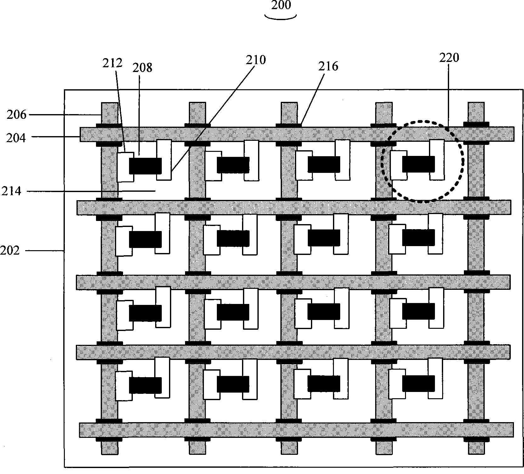
请参阅图1,本技术方案实施例提供一种热发射电子器件200,包括一绝缘基底202,多个热电子发射单元220设置于该绝缘基底202上,以及多个行电极引线204与多个列电极引线206设置于该绝缘基底202上。所述多个行电极引线204与列电极引线206分别平行且等间隔设置于绝缘基底202上。所述多个行电极引线204与多个列电极引线206相互交叉设置,而且,在行电极引线204与列电极引线206交叉处设置有一介质绝缘层216,该介质绝缘层216将行电极引线204与列电极引线206电隔离,以防止短路。每两个相邻的行电极引线204与每两个相邻的列电极引线206形成一网格214,且每个网格214定位一个热电子发射单元220。Please refer to FIG. 1 , the embodiment of the technical solution provides a thermal emission electronic device 200, including an insulating substrate 202, a plurality of thermal electron emission units 220 are arranged on the insulating substrate 202, and a plurality of row electrode leads 204 and a plurality of The column electrode leads 206 are disposed on the insulating substrate 202 . The plurality of row electrode leads 204 and column electrode leads 206 are arranged on the insulating substrate 202 in parallel and equally spaced. The plurality of row electrode leads 204 and the plurality of column electrode leads 206 are arranged to cross each other, and a dielectric insulating layer 216 is arranged at the intersection of the row electrode leads 204 and the column electrode leads 206, and the dielectric insulating layer 216 connects the row electrode leads 204 Electrically isolated from column electrode leads 206 to prevent short circuits. Every two adjacent row electrode leads 204 and every two adjacent column electrode leads 206 form a grid 214 , and each grid 214 locates one thermionic emission unit 220 .
所述多个热电子发射单元220对应设置于上述网格214中,且每个网格214中设置一个热电子发射单元220。每个热电子发射单元220包括一第一电极210,一第二电极212,以及一碳纳米管薄膜结构208。每一行的网格214中的第一电极210与同一行电极引线204电连接,每一列的网格中214的第二电极212与同一列电极引线206电连接。所述第一电极210与第二电极212间隔设置于每个网格214中,并与所述碳纳米管薄膜结构208电连接。所述碳纳米管薄膜结构208至少部分通过所述第一电极210与第二电极212与绝缘基底202间隔设置。本实施例中,同一行的热电子发射单元220中的第一电极210与同一行电极引线204电连接,同一列的热电子发射单元220中的第二电极212与同一列电极引线206电连接。The plurality of thermionic emission units 220 are correspondingly disposed in the grid 214 , and one thermionic emission unit 220 is disposed in each grid 214 . Each thermionic emission unit 220 includes a first electrode 210 , a second electrode 212 , and a carbon nanotube film structure 208 . The first electrodes 210 in each row of grids 214 are electrically connected to the same row electrode leads 204 , and the second electrodes 212 in each column of grids 214 are electrically connected to the same column electrode leads 206 . The first electrode 210 and the second electrode 212 are arranged at intervals in each grid 214 and are electrically connected to the carbon nanotube film structure 208 . The carbon nanotube film structure 208 is at least partly spaced from the insulating substrate 202 by the first electrode 210 and the second electrode 212 . In this embodiment, the first electrodes 210 in the thermionic emission units 220 in the same row are electrically connected to the electrode leads 204 in the same row, and the second electrodes 212 in the thermionic emission units 220 in the same row are electrically connected to the electrode leads 206 in the same column. .
所述的绝缘基底202为一绝缘绝缘基底,如陶瓷绝缘基底、玻璃绝缘基底、树脂绝缘基底、石英绝缘基底等。绝缘基底202大小与厚度不限,本领域技术人员可以根据实际需要选择。本实施例中,绝缘基底202优选为一玻璃绝缘基底,其厚度为大于1毫米,边长大于1厘米。进一步,所述绝缘基底202的表面具有多个对应于所述网格214设置的凹槽。该凹槽等大且等间隔地分布于所述绝缘基底202表面。所述碳纳米管薄膜结构208通过所述绝缘基底202表面的凹槽与所述绝缘基底202间隔设置,从而不会将加热所述碳纳米管薄膜结构208而产生的热量传导进大气中,使所述热发射电子器件200具有优异的热电子发射性能。The insulating substrate 202 is an insulating substrate, such as a ceramic insulating substrate, a glass insulating substrate, a resin insulating substrate, a quartz insulating substrate, and the like. The size and thickness of the insulating base 202 are not limited, and those skilled in the art can select according to actual needs. In this embodiment, the insulating substrate 202 is preferably a glass insulating substrate with a thickness greater than 1 mm and a side length greater than 1 cm. Further, the surface of the insulating base 202 has a plurality of grooves corresponding to the grids 214 . The grooves are equally large and distributed on the surface of the insulating base 202 at equal intervals. The carbon nanotube thin film structure 208 is spaced apart from the insulating substrate 202 through the groove on the surface of the insulating substrate 202, so that the heat generated by heating the carbon nanotube thin film structure 208 will not be conducted into the atmosphere, so that The thermal emission electron device 200 has excellent thermal electron emission performance.
所述多个行电极引线204与多个列电极引线206为一导电体,如金属层等。本实施例中,该多个行电极引线204与多个列电极引线206优选为采用导电浆料印制的平面导电体,且该多个行电极引线204与多个列电极引线206的行距和列距为300微米~500微米。该行电极引线204与列电极引线206的宽度为30微米~100微米,厚度为10微米~50微米。本实施例中,该行电极引线204与列电极引线206的交叉角度为10度到90度,优选为90度。本实施例中,通过丝网印刷法将导电浆料印制于绝缘基底202上制备行电极引线204与列电极引线206。该导电浆料的成分包括金属粉、低熔点玻璃粉和粘结剂。其中,该金属粉优选为银粉,该粘结剂优选为松油醇或乙基纤维素。该导电浆料中,金属粉的重量比为50~90%,低熔点玻璃粉的重量比为2~10%,粘结剂的重量比为10~40%。The plurality of row electrode leads 204 and the plurality of column electrode leads 206 are an electrical conductor, such as a metal layer. In this embodiment, the plurality of row electrode leads 204 and the plurality of column electrode leads 206 are preferably planar conductors printed with conductive paste, and the distance between the plurality of row electrode leads 204 and the plurality of column electrode leads 206 and The row pitch is 300 microns to 500 microns. The row electrode leads 204 and the column electrode leads 206 have a width of 30 microns to 100 microns and a thickness of 10 microns to 50 microns. In this embodiment, the crossing angle between the row electrode leads 204 and the column electrode leads 206 is 10 degrees to 90 degrees, preferably 90 degrees. In this embodiment, the row electrode leads 204 and the column electrode leads 206 are prepared by printing the conductive paste on the insulating substrate 202 by a screen printing method. The components of the conductive paste include metal powder, low-melting glass powder and binder. Wherein, the metal powder is preferably silver powder, and the binder is preferably terpineol or ethyl cellulose. In the conductive paste, the weight ratio of the metal powder is 50-90%, the weight ratio of the low-melting glass powder is 2-10%, and the weight ratio of the binder is 10-40%.
所述第一电极210与第二电极212为一导电体,如金属层等。本实施例中,该第一电极210与第二电极212为一平面导电体,其尺寸依据网格214的尺寸决定。该第一电极210和第二电极212直接与上述电极引线连接,从而实现电连接。所述第一电极210与第二电极212的长度为50微米~90微米,宽度为30微米~60微米,厚度为10微米~50微米。所述第一电极210与第二电极212之间的间隔距离为150微米~450微米。本实施例中,所述第一电极210与第二电极212的长度优选为60微米,宽度优选为40微米,厚度优选为20微米。本实施例中,所述第一电极210与第二电极212的材料为导电浆料,通过丝网印刷法印制于绝缘基底202上。该导电浆料的成分与上述电极引线所用的导电浆料的成分相同。The first electrode 210 and the second electrode 212 are a conductor, such as a metal layer. In this embodiment, the first electrode 210 and the second electrode 212 are a plane conductor whose size is determined according to the size of the grid 214 . The first electrode 210 and the second electrode 212 are directly connected to the above-mentioned electrode leads, so as to realize electrical connection. The length of the first electrode 210 and the second electrode 212 is 50-90 microns, the width is 30-60 microns, and the thickness is 10-50 microns. The distance between the first electrode 210 and the second electrode 212 is 150 microns-450 microns. In this embodiment, the length of the first electrode 210 and the second electrode 212 is preferably 60 microns, the width is preferably 40 microns, and the thickness is preferably 20 microns. In this embodiment, the first electrode 210 and the second electrode 212 are made of conductive paste, which is printed on the insulating substrate 202 by screen printing. The composition of this electroconductive paste is the same as the composition of the electroconductive paste used for the said electrode lead.
所述碳纳米管薄膜结构208包括一碳纳米管薄膜或者至少两个重叠设置的碳纳米管薄膜。该碳纳米管薄膜中的碳纳米管沿同一方向择优取向排列。所述单层碳纳米管薄膜中的碳纳米管沿从所述第一电极210向所述第二电极212延伸的方向排列。所述重叠设置的碳纳米管薄膜中相邻的两个碳纳米管薄膜中的碳纳米管的排列方向具有一交叉角度α,0°≤α≤90°。所述碳纳米管薄膜包括多个首尾相连且择优取向排列的碳纳米管束,相邻的碳纳米管束之间通过范德华力连接。该碳纳米管束包括多个长度相等且相互平行排列的碳纳米管,相邻碳纳米管之间通过范德华力连接。The carbon nanotube film structure 208 includes one carbon nanotube film or at least two overlapping carbon nanotube films. The carbon nanotubes in the carbon nanotube film are preferentially aligned along the same direction. The carbon nanotubes in the single-layer carbon nanotube film are arranged along a direction extending from the first electrode 210 to the second electrode 212 . The arrangement direction of carbon nanotubes in two adjacent carbon nanotube films in the stacked carbon nanotube films has a cross angle α, 0°≤α≤90°. The carbon nanotube film includes a plurality of carbon nanotube bundles connected end to end and arranged in a preferred orientation, and adjacent carbon nanotube bundles are connected by van der Waals force. The carbon nanotube bundle includes a plurality of carbon nanotubes with equal lengths arranged parallel to each other, and the adjacent carbon nanotubes are connected by van der Waals force.
本技术方案实施例中,由于采用CVD法在4英寸的基底上生长超顺排碳纳米管阵列,并进行进一步地处理得到一碳纳米管薄膜,故该碳纳米管薄膜的宽度为0.01厘米~10厘米,厚度为10纳米~100微米。所述碳纳米管薄膜可根据实际需要切割成具有预定尺寸和形状的碳纳米管薄膜。可以理解,当采用较大的基底生长超顺排碳纳米管阵列时,可以得到更宽的碳纳米管薄膜。上述碳纳米管薄膜中的碳纳米管为单壁碳纳米管、双壁碳纳米管或者多壁碳纳米管。当碳纳米管薄膜中的碳纳米管为单壁碳纳米管时,该单壁碳纳米管的直径为0.5纳米~50纳米。当碳纳米管薄膜中的碳纳米管为双壁碳纳米管时,该双壁碳纳米管的直径为1.0纳米~50纳米。当碳纳米管薄膜中的碳纳米管为多壁碳纳米管时,该多壁碳纳米管的直径为1.5纳米~50纳米。所述碳纳米管薄膜结构208与第一电极210和第二电极212的电连接方式可以为通过一导电胶电连接,也可以通过分子间力或者其他方式实现。In the embodiment of the technical solution, since the CVD method is used to grow a super-parallel array of carbon nanotubes on a 4-inch substrate, and further processing is performed to obtain a carbon nanotube film, the width of the carbon nanotube film is 0.01 cm- 10 cm, with a thickness of 10 nanometers to 100 microns. The carbon nanotube film can be cut into carbon nanotube films with a predetermined size and shape according to actual needs. It can be understood that when a larger substrate is used to grow super-parallel carbon nanotube arrays, wider carbon nanotube films can be obtained. The carbon nanotubes in the above carbon nanotube film are single-wall carbon nanotubes, double-wall carbon nanotubes or multi-wall carbon nanotubes. When the carbon nanotubes in the carbon nanotube film are single-wall carbon nanotubes, the diameter of the single-wall carbon nanotubes is 0.5 nanometers to 50 nanometers. When the carbon nanotubes in the carbon nanotube film are double-walled carbon nanotubes, the diameter of the double-walled carbon nanotubes is 1.0 nanometers to 50 nanometers. When the carbon nanotubes in the carbon nanotube film are multi-wall carbon nanotubes, the diameter of the multi-wall carbon nanotubes is 1.5 nanometers to 50 nanometers. The electrical connection between the carbon nanotube film structure 208 and the first electrode 210 and the second electrode 212 may be through a conductive glue, or through intermolecular force or other ways.
另外,所述热发射电子器件200的每个热电子发射单元220可以进一步包括至少一固定电极设置于所述第一电极210和第二电极212,将所述碳纳米管薄膜结构208固定于所述第一电极210和第二电极212。In addition, each thermionic emission unit 220 of the thermal emission electronic device 200 may further include at least one fixed electrode disposed on the first electrode 210 and the second electrode 212, and fix the carbon nanotube thin film structure 208 on the The first electrode 210 and the second electrode 212 are described above.
请参阅图2,本技术方案实施例提供一种上述热发射电子器件200的制备方法,具体包括以下步骤:Please refer to FIG. 2 , the embodiment of the technical solution provides a method for manufacturing the above-mentioned thermal emission electronic device 200, which specifically includes the following steps:
步骤一:提供一绝缘基底202。Step 1: providing an insulating base 202 .
所述的绝缘基底202为一玻璃绝缘基底。进一步,通过刻蚀在所述绝缘基底202表面形成多个等大且等间隔设置的凹槽。The insulating substrate 202 is a glass insulating substrate. Further, a plurality of grooves of equal size and at equal intervals are formed on the surface of the insulating substrate 202 by etching.
步骤二:在该绝缘基底202上制备多个平行且等间隔设置的行电极引线204与列电极引线206,该行电极引线204与列电极引线206交叉设置,且每两个相邻的行电极引线204与每两个相邻的列电极引线206相互交叉形成一网格214。Step 2: Prepare a plurality of parallel and equally spaced row electrode leads 204 and column electrode leads 206 on the insulating substrate 202, the row electrode leads 204 and the column electrode leads 206 are arranged crosswise, and every two adjacent row electrodes The lead wires 204 intersect with every two adjacent column electrode lead wires 206 to form a grid 214 .
可以理解,也可以在所述绝缘基底202上形成多个网格214后再通过刻蚀在所述绝缘基底202表面形成多个等大且等间隔设置的凹槽。该多个凹槽分别与多个网格214对应并设置于所述绝缘基底202上。It can be understood that, after forming a plurality of grids 214 on the insulating substrate 202, a plurality of grooves of equal size and equally spaced can be formed on the surface of the insulating substrate 202 by etching. The plurality of grooves respectively correspond to the plurality of grids 214 and are disposed on the insulating base 202 .
可以通过丝网印刷法、蒸镀法或溅射法等方法制备多个行电极引线204与多个列电极引线206。本实施例中,采用丝网印刷法制备多个行电极引线204与多个列电极引线206,其具体包括以下步骤:A plurality of row electrode leads 204 and a plurality of column electrode leads 206 can be prepared by methods such as screen printing, evaporation or sputtering. In this embodiment, a plurality of row electrode leads 204 and a plurality of column electrode leads 206 are prepared by screen printing, which specifically includes the following steps:
首先,采用丝网印刷法在绝缘基底202上印制多个平行且等间隔设置的行电极引线204。Firstly, a plurality of parallel row electrode leads 204 arranged at equal intervals are printed on the insulating substrate 202 by a screen printing method.
其次,采用丝网印刷法在行电极引线204与待形成的列电极引线206交叉处印制多个介质绝缘层216。Secondly, a plurality of dielectric insulating layers 216 are printed on intersections of the row electrode leads 204 and the column electrode leads 206 to be formed by using a screen printing method.
最后,采用丝网印刷法在绝缘基底202上印制多个平行且等间隔设置的列电极引线206,且多个行电极引线204与多个列电极引线206相互交叉形成多个网格214。Finally, a plurality of parallel and equally spaced column electrode leads 206 are printed on the insulating substrate 202 by screen printing, and a plurality of row electrode leads 204 and a plurality of column electrode leads 206 cross each other to form a plurality of grids 214 .
可以理解,本实施例中,也可以先印制多个平行且等间隔设置的列电极引线206,再印制多个介质绝缘层216,最后印制多个平行且等间隔设置的行电极引线204,且多个行电极引线204与多个列电极引线206相互交叉形成多个网格214。It can be understood that in this embodiment, a plurality of parallel and equally spaced column electrode leads 206 can also be printed first, and then a plurality of dielectric insulating layers 216 can be printed, and finally a plurality of parallel and equally spaced row electrode leads can be printed. 204 , and a plurality of row electrode leads 204 intersect with a plurality of column electrode leads 206 to form a plurality of grids 214 .
步骤三:在所述绝缘基底202上制备多个第一电极210与多个第二电极212,在每个网格214中间隔设置一第一电极210与一第二电极212。Step 3: Prepare a plurality of first electrodes 210 and a plurality of second electrodes 212 on the insulating substrate 202 , and arrange a first electrode 210 and a second electrode 212 in each grid 214 at intervals.
制备多个第一电极210与第二电极212可以通过丝网印刷法、蒸镀法或溅射法等方法实现。本实施例中,采用丝网印刷法制备在每一行的网格214中行电极引线204上制备一第一电极210,该第一电极210与同一行电极引线204形成电连接;通过丝网印刷法、蒸镀法或溅射法在每一列的网格214中列电极引线206上制备一第二电极212,该第二电极212与同一列电极引线206形成电连接。所述第一电极210与第二电极212之间保持一间距,用于设置碳纳米管薄膜结构208。所述第一电极210与第二电极212的厚度大于行电极引线204与列电极引线206的厚度,以利于后续步骤中设置碳纳米管薄膜结构208。可以理解,本实施例中,也可以将所印制的第一电极210与对应的列电极引线206直接接触,从而实现电连接,第二电极212与对应的行电极引线204直接接触,从而实现电连接。The preparation of a plurality of first electrodes 210 and second electrodes 212 can be realized by methods such as screen printing, evaporation or sputtering. In this embodiment, a first electrode 210 is prepared on the row electrode leads 204 in the grid 214 of each row by using the screen printing method, and the first electrode 210 is electrically connected to the same row electrode leads 204; A second electrode 212 is prepared on the column electrode lead 206 in the grid 214 of each column by evaporation or sputtering, and the second electrode 212 is electrically connected to the same column electrode lead 206 . A distance is maintained between the first electrode 210 and the second electrode 212 for setting the carbon nanotube film structure 208 . The thickness of the first electrode 210 and the second electrode 212 is greater than the thickness of the row electrode lead 204 and the column electrode lead 206, so as to facilitate the formation of the carbon nanotube film structure 208 in the subsequent steps. It can be understood that in this embodiment, the printed first electrode 210 can also be directly contacted with the corresponding column electrode lead 206, so as to realize electrical connection, and the second electrode 212 can be directly contacted with the corresponding row electrode lead 204, so as to realize electrical connection.
步骤四:形成一碳纳米管薄膜结构208覆盖上述含有电极和电极引线的绝缘基底202上作为热电子发射体。Step 4: Forming a carbon nanotube film structure 208 covering the above-mentioned insulating substrate 202 containing electrodes and electrode leads as a thermal electron emitter.
所述形成一碳纳米管薄膜结构208覆盖上述含有电极和电极引线的绝缘基底202上作为热电子发射体的方法具体包括以下步骤:The method for forming a carbon nanotube thin film structure 208 covering the above-mentioned insulating substrate 202 containing electrodes and electrode leads as a thermal electron emitter specifically includes the following steps:
(1)制备至少一碳纳米管薄膜。(1) Prepare at least one carbon nanotube film.
首先,提供一碳纳米管阵列,优选地,该阵列为超顺排碳纳米管阵列。Firstly, a carbon nanotube array is provided, preferably, the array is a super-aligned carbon nanotube array.
本实施例中,碳纳米管阵列的制备方法采用化学气相沉积法,其具体步骤包括:(a)提供一平整基底,该基底可选用P型或N型硅基底,或选用形成有氧化层的硅基底,本实施例优选为采用4英寸的硅基底;(b)在基底表面均匀形成一催化剂层,该催化剂层材料可选用铁(Fe)、钴(Co)、镍(Ni)或其任意组合的合金之一;(c)将上述形成有催化剂层的基底在700℃~900℃的空气中退火约30分钟~90分钟;(d)将处理过的基底置于反应炉中,在保护气体环境下加热到500℃~740℃,然后通入碳源气体反应约5分钟~30分钟,生长得到碳纳米管阵列,其高度大于100微米。该碳纳米管阵列为多个彼此平行且垂直于基底生长的碳纳米管形成的纯碳纳米管阵列。该碳纳米管阵列的面积与上述基底面积基本相同。通过上述控制生长条件,该超顺排碳纳米管阵列中基本不含有杂质,如无定型碳或残留的催化剂金属颗粒等。In this embodiment, the preparation method of the carbon nanotube array adopts the chemical vapor deposition method, and the specific steps include: (a) providing a flat substrate, which can be a P-type or N-type silicon substrate, or a silicon substrate with an oxide layer formed on it. Silicon substrate, the present embodiment preferably adopts a 4-inch silicon substrate; (b) uniformly form a catalyst layer on the surface of the substrate, and the catalyst layer material can be selected from iron (Fe), cobalt (Co), nickel (Ni) or any of them One of the combined alloys; (c) annealing the above-mentioned substrate formed with the catalyst layer in the air at 700°C to 900°C for about 30 minutes to 90 minutes; (d) placing the treated substrate in a reaction furnace under protection Heating to 500° C. to 740° C. in a gas environment, and then introducing carbon source gas to react for about 5 minutes to 30 minutes, and growing to obtain a carbon nanotube array, the height of which is greater than 100 microns. The carbon nanotube array is a pure carbon nanotube array formed by a plurality of carbon nanotubes growing parallel to each other and perpendicular to the substrate. The area of the carbon nanotube array is substantially the same as the area of the above-mentioned substrate. By controlling the growth conditions above, the super-aligned carbon nanotube array basically does not contain impurities, such as amorphous carbon or residual catalyst metal particles.
上述碳源气可选用乙炔、乙烯、甲烷等化学性质较活泼的碳氢化合物,本实施例优选的碳源气为乙炔;保护气体为氮气或惰性气体,本实施例优选的保护气体为氩气。The above-mentioned carbon source gas can be selected from acetylene, ethylene, methane and other chemically active hydrocarbons. The preferred carbon source gas in this embodiment is acetylene; the protective gas is nitrogen or an inert gas, and the preferred protective gas in this embodiment is argon. .
可以理解,本实施例提供的碳纳米管阵列不限于上述制备方法,也可为石墨电极恒流电弧放电沉积法、激光蒸发沉积法等。It can be understood that the carbon nanotube array provided in this embodiment is not limited to the above-mentioned preparation method, and may also be a graphite electrode constant current arc discharge deposition method, a laser evaporation deposition method, and the like.
其次,采用一拉伸工具从碳纳米管阵列中拉取获得一碳纳米管薄膜。Secondly, a carbon nanotube film is obtained by pulling from the carbon nanotube array by using a stretching tool.
该碳纳米管薄膜的制备具体包括以下步骤:(a)从上述碳纳米管阵列中选定一定宽度的多个碳纳米管片断,本实施例优选为采用具有一定宽度的胶带接触碳纳米管阵列以选定一定宽度的多个碳纳米管束;(b)以一定速度沿基本垂直于碳纳米管阵列生长方向拉伸多个该碳纳米管束,以形成一连续的碳纳米管薄膜。The preparation of the carbon nanotube film specifically includes the following steps: (a) selecting a plurality of carbon nanotube segments with a certain width from the above-mentioned carbon nanotube array. In this embodiment, an adhesive tape with a certain width is preferably used to contact the carbon nanotube array. Selecting a plurality of carbon nanotube bundles with a certain width; (b) stretching the plurality of carbon nanotube bundles at a certain speed along a direction substantially perpendicular to the growth direction of the carbon nanotube array to form a continuous carbon nanotube film.
在上述拉伸过程中,该多个碳纳米管束在拉力作用下沿拉伸方向逐渐脱离基底的同时,由于范德华力作用,该选定的多个碳纳米管束片断分别与其他碳纳米管束片断首尾相连地连续地被拉出,从而形成一碳纳米管薄膜。该碳纳米管薄膜包括多个首尾相连且定向排列的碳纳米管束,且多个首尾相连且定向排列的碳纳米管束形成一碳纳米管线。该碳纳米管束包括多个平行排列的碳纳米管,且碳纳米管的排列方向基本平行于碳纳米管薄膜的拉伸方向。During the above-mentioned stretching process, while the plurality of carbon nanotube bundles are gradually detached from the substrate along the stretching direction under the action of tension, due to the van der Waals force, the selected plurality of carbon nanotube bundle fragments are respectively connected with other carbon nanotube bundle fragments. The carbon nanotubes are pulled out continuously, forming a carbon nanotube film. The carbon nanotube film includes a plurality of end-to-end and aligned carbon nanotube bundles, and the plurality of end-to-end and aligned carbon nanotube bundles form a carbon nanotube line. The carbon nanotube bundle includes a plurality of carbon nanotubes arranged in parallel, and the arrangement direction of the carbon nanotubes is basically parallel to the stretching direction of the carbon nanotube film.
(2)将上述至少一碳纳米管薄膜铺设于上述含有电极和电极引线的绝缘基底202上形成一碳纳米管薄膜结构208。(2) laying the at least one carbon nanotube film on the insulating substrate 202 containing the electrodes and electrode leads to form a carbon nanotube film structure 208 .
所述将至少一碳纳米管薄膜铺设于所述含有电极和电极引线的绝缘基底202的方法包括以下步骤:将一碳纳米管薄膜或者至少两个碳纳米管薄膜平行且无间隙沿从所述第一电极210向所述第二电极212延伸的方向直接铺设于所述含有电极和电极引线的绝缘基底202的表面。进一步还可将至少两个碳纳米管薄膜依据碳纳米管的排列方向以一交叉角度α重叠铺设于所述含有电极和电极引线的绝缘基底202的表面,0°≤α≤90°。The method for laying at least one carbon nanotube film on the insulating substrate 202 containing electrodes and electrode leads includes the following steps: laying a carbon nanotube film or at least two carbon nanotube films parallel and without gaps along the The first electrode 210 is laid directly on the surface of the insulating base 202 containing the electrodes and electrode leads in a direction extending toward the second electrodes 212 . Further, at least two carbon nanotube films can be overlapped on the surface of the insulating substrate 202 containing electrodes and electrode leads according to the arrangement direction of carbon nanotubes at a cross angle α, 0°≤α≤90°.
可以理解,所述将至少一碳纳米管薄膜铺设于所述含有电极和电极引线的绝缘基底202的方法还可以包括以下步骤:提供一支撑体;将至少两个碳纳米管薄膜平行且无间隙沿从所述第一电极210向所述第二电极212延伸的方向直接铺设于所述支撑体表面,得到一碳纳米管薄膜结构208;去除支撑体外多余的碳纳米管薄膜;采用有机溶剂处理该碳纳米管薄膜结构208;将使用有机溶剂处理后的碳纳米管薄膜结构208从所述支撑体上取下,形成一自支撑的碳纳米管薄膜结构208;将该碳纳米管薄膜结构208铺设于所述含有电极和电极引线的绝缘基底202的表面。进一步还可将至少两个碳纳米管薄膜依据碳纳米管的排列方向以一交叉角度α重叠铺设于所述支撑体表面,0°≤α≤90°。由于本实施例提供的超顺排碳纳米管阵列中的碳纳米管非常纯净,且由于碳纳米管本身的比表面积非常大,所以该碳纳米管薄膜本身具有较强的粘性,该碳纳米管薄膜可利用其本身的粘性直接粘附于支撑体。It can be understood that the method of laying at least one carbon nanotube film on the insulating substrate 202 containing electrodes and electrode leads may also include the following steps: providing a support; placing at least two carbon nanotube films in parallel without gaps Lay directly on the surface of the support along the direction extending from the first electrode 210 to the second electrode 212 to obtain a carbon nanotube film structure 208; remove excess carbon nanotube film outside the support body; treat with an organic solvent The carbon nanotube film structure 208; the carbon nanotube film structure 208 treated with an organic solvent is removed from the support to form a self-supporting carbon nanotube film structure 208; the carbon nanotube film structure 208 laid on the surface of the insulating base 202 containing electrodes and electrode leads. Further, at least two carbon nanotube films can be overlapped and laid on the surface of the support at a cross angle α according to the arrangement direction of the carbon nanotubes, 0°≤α≤90°. Because the carbon nanotubes in the super-parallel carbon nanotube array provided by this embodiment are very pure, and because the specific surface area of the carbon nanotubes itself is very large, the carbon nanotube film itself has strong viscosity, and the carbon nanotubes The film can be directly adhered to the support by its own stickiness.
本实施例中,上述支撑体的大小可依据实际需求确定。当支撑体的宽度大于上述碳纳米管薄膜的宽度时,可以将至少两个碳纳米管薄膜平行且无间隙或/和重叠铺设于所述支撑体,形成一自支撑的碳纳米管薄膜结构208。In this embodiment, the size of the support body can be determined according to actual needs. When the width of the support body is greater than the width of the above-mentioned carbon nanotube film, at least two carbon nanotube films can be laid on the support body in parallel and without gaps or/and overlapping to form a self-supporting carbon nanotube film structure 208 .
本实施例中,由于本实施例步骤四中提供的超顺排碳纳米管阵列中的碳纳米管非常纯净,且由于碳纳米管本身的比表面积非常大,所以该碳纳米管薄膜结构本身具有较强的粘性。该碳纳米管薄膜可利用其本身的粘性直接粘附于所述含有电极和电极引线的绝缘基底202的表面。或者在所述所述含有电极和电极引线的绝缘基底202的表面涂敷一层导电胶;将至少一碳纳米管薄膜于整个含有电极和电极引线的绝缘基底202上,使所述至少一碳纳米管薄膜与所述含有电极和电极引线的绝缘基底202的表面电连接;将大于绝缘基底202面积的碳纳米管薄膜剪去。In this embodiment, since the carbon nanotubes in the super-parallel array of carbon nanotubes provided in Step 4 of this embodiment are very pure, and because the specific surface area of the carbon nanotubes itself is very large, the carbon nanotube film structure itself has Strong viscosity. The carbon nanotube film can be directly adhered to the surface of the insulating substrate 202 containing electrodes and electrode leads by utilizing its own viscosity. Or apply a layer of conductive glue on the surface of the insulating substrate 202 that contains electrodes and electrode leads; at least one carbon nanotube film is placed on the entire insulating substrate 202 that contains electrodes and electrode leads, so that the at least one carbon The nanotube film is electrically connected to the surface of the insulating substrate 202 containing electrodes and electrode leads; the carbon nanotube film with an area larger than the insulating substrate 202 is cut off.
本实施例中,进一步包括采用丝网印刷法制备至少一固定电极(图中未显示)设置于所述第一电极210与第二电极212,将碳纳米管薄膜结构208牢固地固定于所述第一电极210第二电极212上。In this embodiment, it further includes preparing at least one fixed electrode (not shown in the figure) by screen printing method and setting it on the first electrode 210 and the second electrode 212, so as to securely fix the carbon nanotube film structure 208 on the The first electrode 210 is on the second electrode 212 .
另外,本实施例还可进一步在将碳纳米管薄膜直接铺设于所述含有电极和电极引线的绝缘基底形成一碳纳米管薄膜结构208的步骤之后采用有机溶剂处理该碳纳米管薄膜结构208。具体的,可通过试管将有机溶剂滴落在所述碳纳米管薄膜结构208表面浸润整个碳纳米管薄膜结构208。或者,也可将碳纳米管薄膜结构208整个浸入盛有有机溶剂的容器中浸润。该有机溶剂为挥发性有机溶剂,如乙醇、甲醇、丙酮、二氯乙烷或氯仿,本实施例中优选采用乙醇。该碳纳米管薄膜经有机溶剂浸润处理后,在挥发性有机溶剂的表面张力的作用下,碳纳米管薄膜结构208中的平行的碳纳米管片断会部分聚集成碳纳米管束,因此,该碳纳米管薄膜表面体积比小,粘性降低,且具有良好的机械强度及韧性,应用有机溶剂处理后的碳纳米管薄膜性能更加优异。In addition, in this embodiment, the carbon nanotube film structure 208 may be treated with an organic solvent after the step of laying the carbon nanotube film directly on the insulating substrate containing the electrodes and electrode leads to form the carbon nanotube film structure 208 . Specifically, the organic solvent can be dropped on the surface of the carbon nanotube thin film structure 208 through a test tube to wet the entire carbon nanotube thin film structure 208 . Alternatively, the entire carbon nanotube thin film structure 208 may also be immersed in a container containing an organic solvent for infiltration. The organic solvent is a volatile organic solvent, such as ethanol, methanol, acetone, dichloroethane or chloroform, and ethanol is preferably used in this embodiment. After the carbon nanotube film is infiltrated with an organic solvent, under the action of the surface tension of the volatile organic solvent, the parallel carbon nanotube segments in the carbon nanotube film structure 208 will partially gather into carbon nanotube bundles. Therefore, the carbon nanotube The surface volume ratio of the nanotube film is small, the viscosity is reduced, and it has good mechanical strength and toughness. The performance of the carbon nanotube film treated with an organic solvent is even better.
步骤五:切割并去除多余的碳纳米管薄膜结构208,保留每个网格214中覆盖所述第一电极210与第二电极212的碳纳米管薄膜结构208,从而得到一热发射电子器件200。Step 5: cutting and removing the excess carbon nanotube film structure 208, and retaining the carbon nanotube film structure 208 covering the first electrode 210 and the second electrode 212 in each grid 214, thereby obtaining a thermal emission electron device 200 .
所述切割并去除多余的碳纳米管薄膜结构208的方法为激光烧蚀法或电子束扫描法。本实施例中,优选采用激光烧蚀法切割所述碳纳米管薄膜结构208,具体包括以下步骤:The method for cutting and removing the excess carbon nanotube film structure 208 is laser ablation or electron beam scanning. In this embodiment, the carbon nanotube thin film structure 208 is preferably cut by laser ablation, which specifically includes the following steps:
首先,采用一定宽度的激光束沿着每个行电极引线204进行扫描。该步骤的目的是去除不同行的电极(包括第一电极210与第二电极212)之间的碳纳米管薄膜结构208。其中,所述激光束的宽度等于位于不同行的两个相邻的第二电极212之间的行间距离,为100微米~500微米。First, a laser beam of a certain width is used to scan along each row electrode lead 204 . The purpose of this step is to remove the carbon nanotube film structure 208 between electrodes of different rows (including the first electrode 210 and the second electrode 212 ). Wherein, the width of the laser beam is equal to the inter-row distance between two adjacent second electrodes 212 located in different rows, which is 100 micrometers to 500 micrometers.
其次,采用一定宽度的激光束沿着每个列电极引线206进行扫描,去除不同列的电极(包括第一电极210与第二电极212)之间的碳纳米管薄膜结构208。从而保留每个网格214中覆盖所述第一电极210与第二电极212的碳纳米管薄膜结构208。其中,所述激光束的宽度等于位于不同列的两个相邻的第一电极210之间的行间距离,为100微米~500微米。Secondly, a laser beam with a certain width is used to scan along each column electrode lead 206 to remove the carbon nanotube film structure 208 between electrodes of different columns (including the first electrode 210 and the second electrode 212 ). Thus, the carbon nanotube film structure 208 covering the first electrode 210 and the second electrode 212 in each grid 214 remains. Wherein, the width of the laser beam is equal to the row-to-row distance between two adjacent first electrodes 210 in different columns, and is 100 microns to 500 microns.
本实施例中,上述方法可以在大气环境或其它含氧的环境下进行。采用激光烧蚀法去除多余的碳纳米管,所用的激光功率为10瓦~50瓦,扫描速度为10毫米/分钟~1000毫米/分钟。本实施例中,优选地,激光功率为30瓦,扫描速度为100毫米/分钟。In this embodiment, the above method can be carried out in the atmosphere or other oxygen-containing environments. The redundant carbon nanotubes are removed by laser ablation, the laser power used is 10 watts to 50 watts, and the scanning speed is 10 mm/min to 1000 mm/min. In this embodiment, preferably, the laser power is 30 watts, and the scanning speed is 100 mm/min.
与现有技术相比较,所述的热发射电子器件具有以下优点:其一,采用碳纳米管薄膜作为热电子发射体,该碳纳米管薄膜中的碳纳米管均匀分布,所制备的热发射电子器件可以发射均匀而稳定的热电子流;其二,碳纳米管薄膜与绝缘基底间隔设置,绝缘基底不会将加热所述碳纳米管薄膜而产生的热量传导进大气中,故所制备的热发射电子器件的热电子发射性能优异;其三,所述碳纳米管薄膜结构的尺寸小可直接铺设覆盖所述电极,实现热发射电子器件中热电子发射单元的微型化,从而可用于高分辨率和高亮度的平板显示和逻辑电路等多个领域。Compared with the prior art, the thermal emission electronic device has the following advantages: First, the carbon nanotube film is used as the thermal electron emitter, and the carbon nanotubes in the carbon nanotube film are evenly distributed, and the prepared thermal emission The electronic device can emit a uniform and stable thermal electron flow; secondly, the carbon nanotube film is spaced from the insulating substrate, and the insulating substrate will not conduct the heat generated by heating the carbon nanotube film into the atmosphere, so the prepared The thermionic emission performance of the thermal emission electronic device is excellent; third, the size of the carbon nanotube film structure is small and can be directly laid to cover the electrode, so as to realize the miniaturization of the thermal electron emission unit in the thermal emission electronic device, so that it can be used in high High-resolution and high-brightness flat-panel displays and logic circuits and other fields.
另外,本领域技术人员还可在本发明精神内做其他变化,当然,这些依据本发明精神所做的变化,都应包含在本发明所要求保护的范围之内。In addition, those skilled in the art can also make other changes within the spirit of the present invention. Of course, these changes made according to the spirit of the present invention should be included within the scope of protection claimed by the present invention.
Claims (26)
Priority Applications (5)
| Application Number | Priority Date | Filing Date | Title |
|---|---|---|---|
| CN2007101256725A CN101471213B (en) | 2007-12-29 | 2007-12-29 | Thermal emission electronic component and method for producing the same |
| US12/288,864 US8072127B2 (en) | 2007-12-29 | 2008-10-23 | Thermionic electron emission device |
| JP2008320197A JP5015906B2 (en) | 2007-12-29 | 2008-12-16 | THERMOELECTRON EMITTING DEVICE AND METHOD FOR MANUFACTURING THE SAME |
| US13/301,654 US8410675B2 (en) | 2007-12-29 | 2011-11-21 | Thermionic electron emission device |
| US13/301,658 US8808554B2 (en) | 2007-12-29 | 2011-11-21 | Method for making thermionic electron emission device |
Applications Claiming Priority (1)
| Application Number | Priority Date | Filing Date | Title |
|---|---|---|---|
| CN2007101256725A CN101471213B (en) | 2007-12-29 | 2007-12-29 | Thermal emission electronic component and method for producing the same |
Publications (2)
| Publication Number | Publication Date |
|---|---|
| CN101471213A CN101471213A (en) | 2009-07-01 |
| CN101471213B true CN101471213B (en) | 2011-11-09 |
Family
ID=40797316
Family Applications (1)
| Application Number | Title | Priority Date | Filing Date |
|---|---|---|---|
| CN2007101256725A Expired - Fee Related CN101471213B (en) | 2007-12-29 | 2007-12-29 | Thermal emission electronic component and method for producing the same |
Country Status (3)
| Country | Link |
|---|---|
| US (3) | US8072127B2 (en) |
| JP (1) | JP5015906B2 (en) |
| CN (1) | CN101471213B (en) |
Cited By (8)
| Publication number | Priority date | Publication date | Assignee | Title |
|---|---|---|---|---|
| US8406450B2 (en) | 2009-08-28 | 2013-03-26 | Tsinghua University | Thermoacoustic device with heat dissipating structure |
| US8457331B2 (en) | 2009-11-10 | 2013-06-04 | Beijing Funate Innovation Technology Co., Ltd. | Thermoacoustic device |
| US8462965B2 (en) | 2008-12-30 | 2013-06-11 | Beijing Funate Innovation Technology Co., Ltd. | Thermoacoustic module, thermoacoustic device, and method for making the same |
| US8494187B2 (en) | 2009-11-06 | 2013-07-23 | Tsinghua University | Carbon nanotube speaker |
| US8537640B2 (en) | 2009-09-11 | 2013-09-17 | Tsinghua University | Active sonar system |
| US8615096B2 (en) | 2009-08-07 | 2013-12-24 | Tsinghua University | Thermoacoustic device |
| US8811631B2 (en) | 2009-11-16 | 2014-08-19 | Beijing Funate Innovation Technology Co., Ltd. | Thermoacoustic device |
| US8905320B2 (en) | 2009-06-09 | 2014-12-09 | Tsinghua University | Room heating device capable of simultaneously producing sound waves |
Families Citing this family (26)
| Publication number | Priority date | Publication date | Assignee | Title |
|---|---|---|---|---|
| CN101471215B (en) * | 2007-12-29 | 2011-11-09 | 清华大学 | Production method of thermoelectron source |
| CN101471213B (en) | 2007-12-29 | 2011-11-09 | 清华大学 | Thermal emission electronic component and method for producing the same |
| CN101483123B (en) * | 2008-01-11 | 2010-06-02 | 清华大学 | Fabrication method of field emission electronic device |
| US8270639B2 (en) | 2008-04-28 | 2012-09-18 | Tsinghua University | Thermoacoustic device |
| US8259968B2 (en) | 2008-04-28 | 2012-09-04 | Tsinghua University | Thermoacoustic device |
| US8249279B2 (en) | 2008-04-28 | 2012-08-21 | Beijing Funate Innovation Technology Co., Ltd. | Thermoacoustic device |
| US8452031B2 (en) | 2008-04-28 | 2013-05-28 | Tsinghua University | Ultrasonic thermoacoustic device |
| US8259967B2 (en) | 2008-04-28 | 2012-09-04 | Tsinghua University | Thermoacoustic device |
| CN101656907B (en) | 2008-08-22 | 2013-03-20 | 清华大学 | Sound box |
| CN101715160B (en) | 2008-10-08 | 2013-02-13 | 清华大学 | Flexible sound producing device and sound producing flag |
| CN101715155B (en) | 2008-10-08 | 2013-07-03 | 清华大学 | Earphone |
| CN101771922B (en) | 2008-12-30 | 2013-04-24 | 清华大学 | Sounding device |
| US8325947B2 (en) | 2008-12-30 | 2012-12-04 | Bejing FUNATE Innovation Technology Co., Ltd. | Thermoacoustic device |
| CN101943850B (en) | 2009-07-03 | 2013-04-24 | 清华大学 | Sound-producing screen and projection system using same |
| CN102034467B (en) | 2009-09-25 | 2013-01-30 | 北京富纳特创新科技有限公司 | Sound device |
| CN101880035A (en) | 2010-06-29 | 2010-11-10 | 清华大学 | carbon nanotube structure |
| CN102064071B (en) * | 2010-12-16 | 2012-07-18 | 清华大学 | Field emission display device |
| CN103295854B (en) * | 2012-02-23 | 2015-08-26 | 清华大学 | Micro-sharp structure of carbon nano-tube and preparation method thereof |
| CN103515168B (en) * | 2012-06-20 | 2016-01-20 | 清华大学 | Thermal emission electronic component |
| CN103841507B (en) * | 2012-11-20 | 2017-05-17 | 清华大学 | Preparation method for thermotropic sound-making device |
| US10590068B2 (en) | 2016-12-06 | 2020-03-17 | Skeyeon, Inc. | System for producing remote sensing data from near earth orbit |
| US10715245B2 (en) | 2016-12-06 | 2020-07-14 | Skeyeon, Inc. | Radio frequency data downlink for a high revisit rate, near earth orbit satellite system |
| US10351267B2 (en) | 2016-12-06 | 2019-07-16 | Skeyeon, Inc. | Satellite system |
| US10583632B2 (en) | 2018-01-11 | 2020-03-10 | Skeyeon, Inc. | Atomic oxygen-resistant, low drag coatings and materials |
| CN109323784B (en) * | 2018-09-21 | 2020-07-10 | 浙江大学 | Piezoresistive flexible touch sensor with double-layer buckle type micro-boss |
| US11094493B2 (en) | 2019-08-01 | 2021-08-17 | Lockheed Martin Corporation | Emitter structures for enhanced thermionic emission |
Citations (2)
| Publication number | Priority date | Publication date | Assignee | Title |
|---|---|---|---|---|
| US5905335A (en) * | 1995-02-03 | 1999-05-18 | Canon Kabushiki Kaisha | Electron generation using a fluorescent element and image forming using such electron generation |
| CN1773664A (en) * | 2005-09-09 | 2006-05-17 | 清华大学 | Thin film field emitting display device and method for producing its field emission cathode |
Family Cites Families (18)
| Publication number | Priority date | Publication date | Assignee | Title |
|---|---|---|---|---|
| AU665006B2 (en) * | 1991-07-17 | 1995-12-14 | Canon Kabushiki Kaisha | Image-forming device |
| US5955828A (en) * | 1996-10-16 | 1999-09-21 | University Of Utah Research Foundation | Thermionic optical emission device |
| WO2001003208A1 (en) * | 1999-07-02 | 2001-01-11 | President And Fellows Of Harvard College | Nanoscopic wire-based devices, arrays, and methods of their manufacture |
| JP3684173B2 (en) * | 2000-06-30 | 2005-08-17 | キヤノン株式会社 | Manufacturing method of image display device |
| JP3710436B2 (en) * | 2001-09-10 | 2005-10-26 | キヤノン株式会社 | Electron emitting device, electron source, and manufacturing method of image display device |
| JP3857156B2 (en) * | 2002-02-22 | 2006-12-13 | 株式会社日立製作所 | Electron source paste, electron source, and self-luminous panel type display device using the electron source |
| JP4599046B2 (en) | 2003-09-24 | 2010-12-15 | 学校法人 名城大学 | Carbon nanotube filament and use thereof |
| US7465210B2 (en) * | 2004-02-25 | 2008-12-16 | The Regents Of The University Of California | Method of fabricating carbide and nitride nano electron emitters |
| CA2561277A1 (en) * | 2004-03-26 | 2005-10-13 | Foster-Miller, Inc. | Carbon nanotube-based electronic devices made by electronic deposition and applications thereof |
| JP4393257B2 (en) * | 2004-04-15 | 2010-01-06 | キヤノン株式会社 | Envelope manufacturing method and image forming apparatus |
| US20060057388A1 (en) * | 2004-09-10 | 2006-03-16 | Sungho Jin | Aligned and open-ended nanotube structure and method for making the same |
| JP2006260946A (en) * | 2005-03-17 | 2006-09-28 | Hitachi Displays Ltd | Image display device and manufacturing method thereof |
| JP4613327B2 (en) * | 2006-11-06 | 2011-01-19 | 学校法人 名城大学 | Carbon nanotube filament and use thereof |
| CN101459019B (en) * | 2007-12-14 | 2012-01-25 | 清华大学 | Thermal electron source |
| CN101471213B (en) | 2007-12-29 | 2011-11-09 | 清华大学 | Thermal emission electronic component and method for producing the same |
| CN101471211B (en) | 2007-12-29 | 2010-06-02 | 清华大学 | Thermal Emissive Electronics |
| CN101471215B (en) * | 2007-12-29 | 2011-11-09 | 清华大学 | Production method of thermoelectron source |
| CN101471212B (en) * | 2007-12-29 | 2010-12-08 | 清华大学 | Thermal emission electronic component |
-
2007
- 2007-12-29 CN CN2007101256725A patent/CN101471213B/en not_active Expired - Fee Related
-
2008
- 2008-10-23 US US12/288,864 patent/US8072127B2/en active Active
- 2008-12-16 JP JP2008320197A patent/JP5015906B2/en active Active
-
2011
- 2011-11-21 US US13/301,658 patent/US8808554B2/en active Active
- 2011-11-21 US US13/301,654 patent/US8410675B2/en not_active Expired - Fee Related
Patent Citations (2)
| Publication number | Priority date | Publication date | Assignee | Title |
|---|---|---|---|---|
| US5905335A (en) * | 1995-02-03 | 1999-05-18 | Canon Kabushiki Kaisha | Electron generation using a fluorescent element and image forming using such electron generation |
| CN1773664A (en) * | 2005-09-09 | 2006-05-17 | 清华大学 | Thin film field emitting display device and method for producing its field emission cathode |
Non-Patent Citations (1)
| Title |
|---|
| D.C.Cox et al.Thermionic emission from defective carbon nanotubes.《APPLIED PHYSICS LETTERS》.2004,第85卷(第11期), * |
Cited By (9)
| Publication number | Priority date | Publication date | Assignee | Title |
|---|---|---|---|---|
| US8462965B2 (en) | 2008-12-30 | 2013-06-11 | Beijing Funate Innovation Technology Co., Ltd. | Thermoacoustic module, thermoacoustic device, and method for making the same |
| US8763234B2 (en) | 2008-12-30 | 2014-07-01 | Beijing Funate Innovation Technology Co., Ltd. | Method for making thermoacoustic module |
| US8905320B2 (en) | 2009-06-09 | 2014-12-09 | Tsinghua University | Room heating device capable of simultaneously producing sound waves |
| US8615096B2 (en) | 2009-08-07 | 2013-12-24 | Tsinghua University | Thermoacoustic device |
| US8406450B2 (en) | 2009-08-28 | 2013-03-26 | Tsinghua University | Thermoacoustic device with heat dissipating structure |
| US8537640B2 (en) | 2009-09-11 | 2013-09-17 | Tsinghua University | Active sonar system |
| US8494187B2 (en) | 2009-11-06 | 2013-07-23 | Tsinghua University | Carbon nanotube speaker |
| US8457331B2 (en) | 2009-11-10 | 2013-06-04 | Beijing Funate Innovation Technology Co., Ltd. | Thermoacoustic device |
| US8811631B2 (en) | 2009-11-16 | 2014-08-19 | Beijing Funate Innovation Technology Co., Ltd. | Thermoacoustic device |
Also Published As
| Publication number | Publication date |
|---|---|
| JP2009164119A (en) | 2009-07-23 |
| US8808554B2 (en) | 2014-08-19 |
| US20120062100A1 (en) | 2012-03-15 |
| US8072127B2 (en) | 2011-12-06 |
| JP5015906B2 (en) | 2012-09-05 |
| US8410675B2 (en) | 2013-04-02 |
| US20090167137A1 (en) | 2009-07-02 |
| CN101471213A (en) | 2009-07-01 |
| US20120064794A1 (en) | 2012-03-15 |
Similar Documents
| Publication | Publication Date | Title |
|---|---|---|
| CN101471213B (en) | Thermal emission electronic component and method for producing the same | |
| CN101471211B (en) | Thermal Emissive Electronics | |
| CN101471212B (en) | Thermal emission electronic component | |
| CN101483123B (en) | Fabrication method of field emission electronic device | |
| CN101499389B (en) | Electronic emitter | |
| CN101471215B (en) | Production method of thermoelectron source | |
| CN101499390B (en) | Electronic emitter and method for producing the same | |
| JP5209659B2 (en) | Incandescent light source display device | |
| CN101425438A (en) | Producing method for field emission type electron source | |
| CN101471210B (en) | hot electron source | |
| TWI330858B (en) | Thermionic emission device | |
| TWI352369B (en) | Thermionic emission device and method for making t | |
| CN103730303B (en) | Field emission electron source array and field emission apparatus | |
| TWI352371B (en) | Method for making field emission electron device | |
| TWI360831B (en) | Field emission electron device | |
| TWI417924B (en) | Field emission electronic device | |
| TW200937484A (en) | Electron emission device and method for making the same | |
| TW200932665A (en) | Thermionic emission device |
Legal Events
| Date | Code | Title | Description |
|---|---|---|---|
| C06 | Publication | ||
| PB01 | Publication | ||
| C10 | Entry into substantive examination | ||
| SE01 | Entry into force of request for substantive examination | ||
| C14 | Grant of patent or utility model | ||
| GR01 | Patent grant | ||
| CF01 | Termination of patent right due to non-payment of annual fee | ||
| CF01 | Termination of patent right due to non-payment of annual fee |
Granted publication date: 20111109 |