CN101390208A - contact formation - Google Patents
contact formation Download PDFInfo
- Publication number
- CN101390208A CN101390208A CNA2007800068498A CN200780006849A CN101390208A CN 101390208 A CN101390208 A CN 101390208A CN A2007800068498 A CNA2007800068498 A CN A2007800068498A CN 200780006849 A CN200780006849 A CN 200780006849A CN 101390208 A CN101390208 A CN 101390208A
- Authority
- CN
- China
- Prior art keywords
- contact
- groove
- electric conducting
- contacts
- conducting material
- Prior art date
- Legal status (The legal status is an assumption and is not a legal conclusion. Google has not performed a legal analysis and makes no representation as to the accuracy of the status listed.)
- Granted
Links
- 230000015572 biosynthetic process Effects 0.000 title claims description 14
- 239000000463 material Substances 0.000 claims abstract description 156
- 238000000034 method Methods 0.000 claims abstract description 84
- 239000004020 conductor Substances 0.000 claims abstract description 55
- 125000006850 spacer group Chemical group 0.000 claims abstract description 37
- 239000012212 insulator Substances 0.000 claims abstract description 28
- 239000004065 semiconductor Substances 0.000 claims description 25
- 239000000758 substrate Substances 0.000 claims description 21
- 239000000945 filler Substances 0.000 claims description 20
- 239000011810 insulating material Substances 0.000 claims description 10
- 238000003860 storage Methods 0.000 claims description 10
- 229910021420 polycrystalline silicon Inorganic materials 0.000 claims description 7
- 229910052721 tungsten Inorganic materials 0.000 claims description 7
- 239000010937 tungsten Substances 0.000 claims description 7
- RTAQQCXQSZGOHL-UHFFFAOYSA-N Titanium Chemical compound [Ti] RTAQQCXQSZGOHL-UHFFFAOYSA-N 0.000 claims description 6
- NRTOMJZYCJJWKI-UHFFFAOYSA-N Titanium nitride Chemical compound [Ti]#N NRTOMJZYCJJWKI-UHFFFAOYSA-N 0.000 claims description 6
- 230000008021 deposition Effects 0.000 claims description 6
- 238000000059 patterning Methods 0.000 claims description 6
- 238000011049 filling Methods 0.000 claims description 5
- 229910052581 Si3N4 Inorganic materials 0.000 claims description 4
- HQVNEWCFYHHQES-UHFFFAOYSA-N silicon nitride Chemical compound N12[Si]34N5[Si]62N3[Si]51N64 HQVNEWCFYHHQES-UHFFFAOYSA-N 0.000 claims description 4
- 239000010936 titanium Substances 0.000 claims description 4
- 229910052719 titanium Inorganic materials 0.000 claims description 4
- WFKWXMTUELFFGS-UHFFFAOYSA-N tungsten Chemical compound [W] WFKWXMTUELFFGS-UHFFFAOYSA-N 0.000 claims description 4
- BOTDANWDWHJENH-UHFFFAOYSA-N Tetraethyl orthosilicate Chemical compound CCO[Si](OCC)(OCC)OCC BOTDANWDWHJENH-UHFFFAOYSA-N 0.000 claims description 3
- -1 Tungsten nitride Chemical class 0.000 claims description 3
- 238000005516 engineering process Methods 0.000 claims description 3
- 239000003989 dielectric material Substances 0.000 claims description 2
- 230000002093 peripheral effect Effects 0.000 claims description 2
- 239000002210 silicon-based material Substances 0.000 claims description 2
- 238000000151 deposition Methods 0.000 abstract description 14
- 239000010410 layer Substances 0.000 description 54
- 238000005755 formation reaction Methods 0.000 description 12
- 230000004888 barrier function Effects 0.000 description 6
- 238000005530 etching Methods 0.000 description 6
- 238000004519 manufacturing process Methods 0.000 description 6
- 229920005591 polysilicon Polymers 0.000 description 6
- VYPSYNLAJGMNEJ-UHFFFAOYSA-N Silicium dioxide Chemical compound O=[Si]=O VYPSYNLAJGMNEJ-UHFFFAOYSA-N 0.000 description 5
- 229910052751 metal Inorganic materials 0.000 description 5
- 239000002184 metal Substances 0.000 description 5
- 150000004767 nitrides Chemical class 0.000 description 5
- 238000001465 metallisation Methods 0.000 description 4
- XUIMIQQOPSSXEZ-UHFFFAOYSA-N Silicon Chemical compound [Si] XUIMIQQOPSSXEZ-UHFFFAOYSA-N 0.000 description 3
- 239000003990 capacitor Substances 0.000 description 3
- 230000002829 reductive effect Effects 0.000 description 3
- 229910052710 silicon Inorganic materials 0.000 description 3
- 239000010703 silicon Substances 0.000 description 3
- 230000009286 beneficial effect Effects 0.000 description 2
- 238000005229 chemical vapour deposition Methods 0.000 description 2
- 230000012447 hatching Effects 0.000 description 2
- 230000000873 masking effect Effects 0.000 description 2
- 230000036961 partial effect Effects 0.000 description 2
- 239000011241 protective layer Substances 0.000 description 2
- 239000000377 silicon dioxide Substances 0.000 description 2
- 235000012239 silicon dioxide Nutrition 0.000 description 2
- 206010010144 Completed suicide Diseases 0.000 description 1
- OAICVXFJPJFONN-UHFFFAOYSA-N Phosphorus Chemical compound [P] OAICVXFJPJFONN-UHFFFAOYSA-N 0.000 description 1
- 230000006978 adaptation Effects 0.000 description 1
- 239000000853 adhesive Substances 0.000 description 1
- 230000001070 adhesive effect Effects 0.000 description 1
- 229910052782 aluminium Inorganic materials 0.000 description 1
- XAGFODPZIPBFFR-UHFFFAOYSA-N aluminium Chemical compound [Al] XAGFODPZIPBFFR-UHFFFAOYSA-N 0.000 description 1
- 238000003491 array Methods 0.000 description 1
- 230000000712 assembly Effects 0.000 description 1
- 238000000429 assembly Methods 0.000 description 1
- 238000000576 coating method Methods 0.000 description 1
- 239000010941 cobalt Substances 0.000 description 1
- 229910017052 cobalt Inorganic materials 0.000 description 1
- GUTLYIVDDKVIGB-UHFFFAOYSA-N cobalt atom Chemical compound [Co] GUTLYIVDDKVIGB-UHFFFAOYSA-N 0.000 description 1
- 239000002131 composite material Substances 0.000 description 1
- 238000000280 densification Methods 0.000 description 1
- 238000009792 diffusion process Methods 0.000 description 1
- 230000006870 function Effects 0.000 description 1
- 239000011521 glass Substances 0.000 description 1
- 239000003292 glue Substances 0.000 description 1
- 238000003384 imaging method Methods 0.000 description 1
- 239000007943 implant Substances 0.000 description 1
- 238000009413 insulation Methods 0.000 description 1
- 238000002955 isolation Methods 0.000 description 1
- 238000002161 passivation Methods 0.000 description 1
- 229910052698 phosphorus Inorganic materials 0.000 description 1
- 239000011574 phosphorus Substances 0.000 description 1
- 238000000206 photolithography Methods 0.000 description 1
- 239000003870 refractory metal Substances 0.000 description 1
- 229910052594 sapphire Inorganic materials 0.000 description 1
- 239000010980 sapphire Substances 0.000 description 1
- 229910021332 silicide Inorganic materials 0.000 description 1
- FVBUAEGBCNSCDD-UHFFFAOYSA-N silicide(4-) Chemical compound [Si-4] FVBUAEGBCNSCDD-UHFFFAOYSA-N 0.000 description 1
- 229910052814 silicon oxide Inorganic materials 0.000 description 1
- 230000003068 static effect Effects 0.000 description 1
- MZLGASXMSKOWSE-UHFFFAOYSA-N tantalum nitride Chemical compound [Ta]#N MZLGASXMSKOWSE-UHFFFAOYSA-N 0.000 description 1
- 229910021341 titanium silicide Inorganic materials 0.000 description 1
- WQJQOUPTWCFRMM-UHFFFAOYSA-N tungsten disilicide Chemical compound [Si]#[W]#[Si] WQJQOUPTWCFRMM-UHFFFAOYSA-N 0.000 description 1
- 229910021342 tungsten silicide Inorganic materials 0.000 description 1
Images


Classifications
-
- H—ELECTRICITY
- H01—ELECTRIC ELEMENTS
- H01L—SEMICONDUCTOR DEVICES NOT COVERED BY CLASS H10
- H01L21/00—Processes or apparatus adapted for the manufacture or treatment of semiconductor or solid state devices or of parts thereof
- H01L21/70—Manufacture or treatment of devices consisting of a plurality of solid state components formed in or on a common substrate or of parts thereof; Manufacture of integrated circuit devices or of parts thereof
- H01L21/71—Manufacture of specific parts of devices defined in group H01L21/70
- H01L21/768—Applying interconnections to be used for carrying current between separate components within a device comprising conductors and dielectrics
- H01L21/76801—Applying interconnections to be used for carrying current between separate components within a device comprising conductors and dielectrics characterised by the formation and the after-treatment of the dielectrics, e.g. smoothing
- H01L21/76802—Applying interconnections to be used for carrying current between separate components within a device comprising conductors and dielectrics characterised by the formation and the after-treatment of the dielectrics, e.g. smoothing by forming openings in dielectrics
- H01L21/76804—Applying interconnections to be used for carrying current between separate components within a device comprising conductors and dielectrics characterised by the formation and the after-treatment of the dielectrics, e.g. smoothing by forming openings in dielectrics by forming tapered via holes
-
- H—ELECTRICITY
- H01—ELECTRIC ELEMENTS
- H01L—SEMICONDUCTOR DEVICES NOT COVERED BY CLASS H10
- H01L21/00—Processes or apparatus adapted for the manufacture or treatment of semiconductor or solid state devices or of parts thereof
- H01L21/70—Manufacture or treatment of devices consisting of a plurality of solid state components formed in or on a common substrate or of parts thereof; Manufacture of integrated circuit devices or of parts thereof
- H01L21/71—Manufacture of specific parts of devices defined in group H01L21/70
- H01L21/768—Applying interconnections to be used for carrying current between separate components within a device comprising conductors and dielectrics
- H01L21/76801—Applying interconnections to be used for carrying current between separate components within a device comprising conductors and dielectrics characterised by the formation and the after-treatment of the dielectrics, e.g. smoothing
- H01L21/76829—Applying interconnections to be used for carrying current between separate components within a device comprising conductors and dielectrics characterised by the formation and the after-treatment of the dielectrics, e.g. smoothing characterised by the formation of thin functional dielectric layers, e.g. dielectric etch-stop, barrier, capping or liner layers
- H01L21/76831—Applying interconnections to be used for carrying current between separate components within a device comprising conductors and dielectrics characterised by the formation and the after-treatment of the dielectrics, e.g. smoothing characterised by the formation of thin functional dielectric layers, e.g. dielectric etch-stop, barrier, capping or liner layers in via holes or trenches, e.g. non-conductive sidewall liners
-
- H—ELECTRICITY
- H10—SEMICONDUCTOR DEVICES; ELECTRIC SOLID-STATE DEVICES NOT OTHERWISE PROVIDED FOR
- H10B—ELECTRONIC MEMORY DEVICES
- H10B12/00—Dynamic random access memory [DRAM] devices
- H10B12/01—Manufacture or treatment
- H10B12/02—Manufacture or treatment for one transistor one-capacitor [1T-1C] memory cells
- H10B12/03—Making the capacitor or connections thereto
- H10B12/033—Making the capacitor or connections thereto the capacitor extending over the transistor
- H10B12/0335—Making a connection between the transistor and the capacitor, e.g. plug
-
- H—ELECTRICITY
- H10—SEMICONDUCTOR DEVICES; ELECTRIC SOLID-STATE DEVICES NOT OTHERWISE PROVIDED FOR
- H10B—ELECTRONIC MEMORY DEVICES
- H10B12/00—Dynamic random access memory [DRAM] devices
- H10B12/30—DRAM devices comprising one-transistor - one-capacitor [1T-1C] memory cells
- H10B12/48—Data lines or contacts therefor
- H10B12/485—Bit line contacts
-
- H—ELECTRICITY
- H10—SEMICONDUCTOR DEVICES; ELECTRIC SOLID-STATE DEVICES NOT OTHERWISE PROVIDED FOR
- H10D—INORGANIC ELECTRIC SEMICONDUCTOR DEVICES
- H10D89/00—Aspects of integrated devices not covered by groups H10D84/00 - H10D88/00
- H10D89/10—Integrated device layouts
Landscapes
- Engineering & Computer Science (AREA)
- Manufacturing & Machinery (AREA)
- Microelectronics & Electronic Packaging (AREA)
- General Physics & Mathematics (AREA)
- Condensed Matter Physics & Semiconductors (AREA)
- Computer Hardware Design (AREA)
- Physics & Mathematics (AREA)
- Power Engineering (AREA)
- Internal Circuitry In Semiconductor Integrated Circuit Devices (AREA)
- Semiconductor Memories (AREA)
- Manufacturing Of Electrical Connectors (AREA)
- Metal-Oxide And Bipolar Metal-Oxide Semiconductor Integrated Circuits (AREA)
- Electrodes Of Semiconductors (AREA)
Abstract
本发明包含各种方法、电路、装置和系统实施例。一个此类方法实施例包含:在绝缘体堆叠材料(222)中创建沟槽(527),其中所述沟槽的一部分定位在多个栅极(112)中的两个栅极之间;以及将间隔物材料(630)沉积到所述沟槽的至少一个侧表面。此方法还包含:将导电材料(732、834)沉积到所述沟槽中;以及将盖材料沉积到所述沟槽中。
The invention encompasses various method, circuit, apparatus and system embodiments. One such method embodiment includes: creating a trench (527) in the insulator stack material (222), wherein a portion of the trench is positioned between two gates of the plurality of gates (112); and A spacer material (630) is deposited to at least one side surface of the trench. The method also includes: depositing (732, 834) a conductive material into the trenches; and depositing a capping material into the trenches.
Description
技术领域 technical field
本发明大体上涉及半导体装置,且更明确地说,涉及供存储器、图像、逻辑和其它半导体装置中使用的触点处理技术。The present invention relates generally to semiconductor devices, and more particularly to contact processing techniques for use in memory, graphics, logic and other semiconductor devices.
背景技术 Background technique
实施电子电路涉及通过特定的电子路径来连接隔离的装置或电路组件。在硅集成电路(IC)制造中,形成于单个衬底中的电路组件通常彼此隔离。随后可互连各个电路组件,以创建特定的电路配置。Implementing an electronic circuit involves connecting isolated devices or circuit components through specific electronic paths. In silicon integrated circuit (IC) fabrication, circuit components formed in a single substrate are typically isolated from each other. The various circuit components can then be interconnected to create specific circuit configurations.
集成电路行业在电子电路致密化和小型化方面不断进步。这种进步已经导致了日益紧凑且高效的半导体装置,这又实现使这些装置并入其中的系统更小且消耗的功率更少。The integrated circuit industry continues to advance in the densification and miniaturization of electronic circuits. Such advances have led to increasingly compact and efficient semiconductor devices, which in turn enables the systems into which these devices are incorporated to be smaller and consume less power.
在形成半导体装置(例如动态随机存取存储器(DRAM)、静态随机存取存储器(SRAM)、微处理器等)期间,可使用绝缘层(例如二氧化硅、掺杂有磷的二氧化硅或其它材料)来电隔离导电层,例如掺杂多晶硅、掺杂硅、铝、耐熔金属硅化物和由其它导电材料形成的层。During the formation of semiconductor devices such as dynamic random access memory (DRAM), static random access memory (SRAM), microprocessors, etc., insulating layers such as silicon dioxide, silicon dioxide doped with phosphorus, or other materials) to electrically isolate conductive layers such as doped polysilicon, doped silicon, aluminum, refractory metal suicides, and layers formed of other conductive materials.
在制造电子电路的过程中,将材料层施加在彼此上方,以向电路提供各种特征。在此过程期间,为了使下面的层可被接近,可移除部分或全部层。在一些制造方法中,可使用额外材料来填充在被移除的部分中。此分层和移除过程可包含沉积、蚀刻、平面化、光刻以及其它过程。During the manufacture of electronic circuits, layers of material are applied over each other to provide various features to the circuit. During this process, some or all of the layers may be removed in order to make the underlying layers accessible. In some manufacturing methods, additional material may be used to fill in the removed portion. This layering and removal process may include deposition, etching, planarization, photolithography, and other processes.
在许多装置中,可通过绝缘层中的开口来互连导电层。此些开口通常被称为触点开口(例如,当开口延伸穿过绝缘层到达有源装置区域时)。一般来说,此些开口还被称为孔或通孔(即,当开口延伸穿过两个导电层之间的绝缘层时)。In many devices, conductive layers may be interconnected through openings in insulating layers. Such openings are often referred to as contact openings (eg, when the opening extends through the insulating layer to the active device area). In general, such openings are also referred to as holes or vias (ie, when the opening extends through an insulating layer between two conductive layers).
除了尺寸之外,制造过程所花费的时间和所使用的材料可能是电路设计中的重要因素。举例来说,可改变的且可能对制造过程有益的方面包含分层过程的数目、执行所述过程所花费的时间和/或这些过程中所使用的材料量可减少。In addition to size, the time it takes for the fabrication process and the materials used can be important factors in circuit design. For example, aspects that may be changed and may be beneficial to the manufacturing process include that the number of layering processes, the time it takes to perform the processes, and/or the amount of material used in these processes may be reduced.
发明内容 Contents of the invention
无none
附图说明 Description of drawings
从下文参考附图详细描述的实施例的具体实施方式中将容易了解本发明的特征和优点,其中:The features and advantages of the present invention will become readily apparent from the detailed description of the embodiments described in detail below with reference to the accompanying drawings, in which:
图1是根据本发明的正在处理中的触点结构的实施例的示范性部分的横截面图。1 is a cross-sectional view of an exemplary portion of an embodiment of a contact structure in process according to the present invention.
图2是在沉积绝缘体材料之后图1中的触点结构的实施例的示范性部分的横截面图。2 is a cross-sectional view of an exemplary portion of the embodiment of the contact structure in FIG. 1 after depositing an insulator material.
图3是在形成多个触点开口之后图2中的触点结构的实施例的示范性部分的横截面图。3 is a cross-sectional view of an exemplary portion of the embodiment of the contact structure in FIG. 2 after forming a plurality of contact openings.
图4是在用填充物材料填充之后图3中的触点结构的实施例的示范性部分的横截面图。4 is a cross-sectional view of an exemplary portion of the embodiment of the contact structure in FIG. 3 after filling with a filler material.
图5A是在形成沟槽结构之后从图4中的触点结构的实施例的上部视角观看的多个数字和单元触点的定位的表示。5A is a representation of the positioning of a plurality of digit and cell contacts from an upper perspective of the embodiment of the contact structure in FIG. 4 after formation of the trench structure.
图5B是在形成沟槽结构之后图4中的触点结构的实施例的示范性部分的横截面图。5B is a cross-sectional view of an exemplary portion of the embodiment of the contact structure in FIG. 4 after forming the trench structure.
图5C是在使用牺牲材料的情况下在形成沟槽结构之后图4中的触点结构的实施例的示范性部分的横截面图。5C is an exemplary partial cross-sectional view of the embodiment of the contact structure in FIG. 4 after formation of the trench structure using a sacrificial material.
图6是在施加间隔物材料之后图5中的触点结构的实施例的示范性部分的横截面图。6 is a cross-sectional view of an exemplary portion of the embodiment of the contact structure in FIG. 5 after application of spacer material.
图7是在施加衬垫材料之后图6中的触点结构的实施例的示范性部分的横截面图。7 is a cross-sectional view of an exemplary portion of the embodiment of the contact structure in FIG. 6 after application of a liner material.
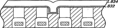
图8是在施加导体材料之后图7中的触点结构的实施例的示范性部分的横截面图。8 is a cross-sectional view of an exemplary portion of the embodiment of the contact structure in FIG. 7 after application of conductor material.
图9是在对导体材料进行平面化之后图8中的触点结构的实施例的示范性部分的横截面图。9 is a cross-sectional view of an exemplary portion of the embodiment of the contact structure in FIG. 8 after planarization of the conductor material.
图10是在形成凹口并施加盖材料之后图9中的触点结构的实施例的示范性部分的横截面图。10 is a cross-sectional view of an exemplary portion of the embodiment of the contact structure in FIG. 9 after forming a recess and applying a cover material.
图11是包含本发明的触点结构的实施例的示范性集成电路的横截面图。11 is a cross-sectional view of an exemplary integrated circuit incorporating an embodiment of the contact structure of the present invention.
图12是可包含本发明的触点结构的实施例的示范性电子系统。Figure 12 is an exemplary electronic system that may incorporate an embodiment of the contact structure of the present invention.
具体实施方式 Detailed ways
本发明包含各种方法、电路、装置和系统实施例。本文所揭示的各种实施例可用于减少分层过程的数目、执行所述过程所花费的时间和/或这些过程中所使用的材料量可减少,以及其它益处。The invention encompasses various method, circuit, apparatus and system embodiments. Various embodiments disclosed herein can be used to reduce the number of layering processes, the time it takes to perform the processes and/or the amount of material used in these processes can be reduced, among other benefits.
一个此类方法实施例包含:在绝缘体堆叠材料中创建沟槽,所述沟槽的一部分定位在多个栅极中的两个栅极之间;以及将间隔物材料沉积到所述沟槽的至少一个侧表面。此方法还包含:将导电材料沉积到沟槽中;以及将盖材料沉积到沟槽中。One such method embodiment includes: creating a trench in an insulator stack material, a portion of the trench positioned between two gates of the plurality of gates; and depositing a spacer material into the trench at least one side surface. The method also includes: depositing a conductive material into the trenches; and depositing a capping material into the trenches.
在一些实施例中,所述多个栅极每一者可具有盖,所述盖的高度为1500埃或更小。实施例可包含创建多个栅极,举例来说,其每一者具有盖,所述盖的高度近似为700埃。在各个实施例中,所述多个栅极每一者可具有盖,所述盖的高度为700埃或更小。In some embodiments, each of the plurality of gates may have a cap having a height of 1500 Angstroms or less. Embodiments may include creating multiple gates, each having a cap, for example, with a height of approximately 700 Angstroms. In various embodiments, each of the plurality of gates may have a cap having a height of 700 Angstroms or less.
如本文所使用的术语“衬底”或“衬底组合件”指代半导体衬底,例如基底半导体层或上面形成有一个或一个以上层、结构和/或区的半导体衬底。基底半导体层通常是晶片上最下面的硅材料层或沉积在另一材料(例如蓝宝石上硅)上的硅层。当提到衬底组合件时,先前可能已经使用了各种处理步骤来形成或界定区、结、各种结构/特征和/或开口,例如电容器极板和/或用于电容器的阻挡层。The term "substrate" or "substrate assembly" as used herein refers to a semiconductor substrate, such as a base semiconductor layer or a semiconductor substrate on which one or more layers, structures and/or regions are formed. The base semiconductor layer is typically the lowest layer of silicon material on the wafer or a layer of silicon deposited on another material such as silicon-on-sapphire. When referring to substrate assemblies, various processing steps may have previously been used to form or define regions, junctions, various structures/features and/or openings, such as capacitor plates and/or barrier layers for capacitors.
如本文所使用的“层”指代任何可使用沉积或其它过程形成于衬底上的层。术语“层”意欲包含专用于半导体行业的层,例如“阻挡层”、“介电层”和“导电层”。(术语“层”与半导体行业中所使用的术语“膜”同义)。术语“层”还意欲包含在半导体技术之外的技术中发现的层(例如玻璃上涂层)。A "layer" as used herein refers to any layer that may be formed on a substrate using deposition or other processes. The term "layer" is intended to include layers specific to the semiconductor industry, such as "barrier layers", "dielectric layers" and "conductive layers". (The term "layer" is synonymous with the term "film" used in the semiconductor industry). The term "layer" is also intended to include layers found in technologies other than semiconductor technology (eg, coatings on glass).
在图中,参考编号中的第一个数字或两个数字(即,三位数的第一个数字和四位数的前两个数字)指代其在里面使用的图,而参考编号的其余两个数字指代贯穿附图的若干个图而使用的本发明实施例的相同或等效部分。所述图的比例并不代表其中所说明的各个元件的精确尺寸。In the figures, the first digit or two digits of a reference number (i.e., the first digit of the three-digit number and the first two digits of the four-digit number) designate the figure in which it is used, while the reference number's The remaining two numbers refer to the same or equivalent parts of the embodiments of the invention used throughout the several figures of the drawings. The scale of the drawings does not imply precise dimensions of the various elements illustrated therein.
现将参考附图详细描述本发明的实施例。应注意,尽管所述图说明形成一个导体,但本文所预期的各种实施例中可形成有任何数目的导体。Embodiments of the present invention will now be described in detail with reference to the accompanying drawings. It should be noted that although the figures illustrate the formation of one conductor, any number of conductors may be formed in various embodiments contemplated herein.
图1是根据本发明的正在处理中的触点结构的实施例的示范性部分的横截面图。在此实施例中,多个栅极结构112、116、118和120已经形成于衬底110上。1 is a cross-sectional view of an exemplary portion of an embodiment of a contact structure in process according to the present invention. In this embodiment, a plurality of
在图1中所说明的实施例中,每一栅极结构包含多晶硅结构114,其可用作触点或触点的一部分。尽管说明了特定类型的栅极结构,但在本发明的各种实施例中可使用各种类型的栅极结构。另外,在各种实施例中,可在衬底110内在上面形成有栅极112、116、118和120的层级下方形成组件。In the embodiment illustrated in FIG. 1, each gate structure includes a
在本发明的各种实施例中,有可能形成厚度小于1500埃(A)的栅极盖(例如,图1的栅极盖115)。在许多触点制造过程中,栅极盖厚度至少为1500A,因为所述盖可能暴露于一个或一个以上平面化过程。In various embodiments of the invention, it is possible to form a gate cap (eg,
如本文所论述,在本发明的一些实施例中,可在不使盖暴露于平面化过程的情况下形成触点。因此,可减小盖厚度。举例来说,在一些实施例中,盖厚度可近似为700A。这在以下方面可能是有益的:便于对栅极或触点结构进行图案化;减小组件的垂直尺寸;减少用于触点形成的时间;减小所利用的材料量;以及其它益处。As discussed herein, in some embodiments of the invention, contacts may be formed without exposing the lid to the planarization process. Therefore, the cover thickness can be reduced. For example, in some embodiments, the cover thickness may be approximately 700A. This may be beneficial in terms of: facilitating patterning of the gate or contact structures; reducing the vertical dimension of the component; reducing the time for contact formation; reducing the amount of material utilized; among other benefits.
在已经形成栅极之后,可沉积绝缘体材料。举例来说,图2是在沉积绝缘体材料之后图1中的触点结构的实施例的示范性部分的横截面图。如图2中所示,绝缘体材料222沉积在栅极212、216、218和220上方,以形成绝缘体堆叠层。这可(例如)通过沉积阻挡层(例如,薄氮化物层,图2中未图示)和电介质上旋涂(SOD)来完成。After the gate has been formed, an insulator material can be deposited. For example, FIG. 2 is a cross-sectional view of an exemplary portion of the embodiment of the contact structure in FIG. 1 after depositing an insulator material. As shown in FIG. 2 , an
在各种实施例中,可沉积较厚的绝缘体材料层。举例来说,在一些实施例中,层222的厚度217在栅极的顶表面上可为1800A。当被施加时,可对绝缘体材料的上表面进行平面化,以提供大致均匀的厚度。In various embodiments, thicker layers of insulator material may be deposited. For example, in some embodiments,
图3是在形成多个触点开口之后图2中的触点结构的实施例的示范性部分的横截面图。在图3的实施例中,可在绝缘体堆叠层322中形成触点开口324。3 is a cross-sectional view of an exemplary portion of the embodiment of the contact structure in FIG. 2 after forming a plurality of contact openings. In the embodiment of FIG. 3 ,
可(例如)通过掩蔽工艺(例如,双掩蔽工艺)对阵列中的离散触点进行图案化来完成触点开口的形成。这些触点开口可用于界定单元触点和数字触点。可以多种方式来完成触点开口的形成。举例来说,可使用各种蚀刻技术来蚀刻到绝缘体层中。Formation of the contact openings can be accomplished, for example, by patterning the discrete contacts in the array by a masking process (eg, a double masking process). These contact openings can be used to define unit contacts and digital contacts. Formation of the contact openings can be accomplished in a number of ways. For example, various etching techniques can be used to etch into the insulator layer.
在一些实施例中,可组合多种蚀刻技术来形成触点开口。举例来说,在一些实施例中,可使用触点干式蚀刻来为触点开口的深度的一部分(例如,约1500A的深度)形成大致直立的壁,接着使用SAC型蚀刻以沿栅极的侧面形成触点(例如,图3的栅极312、316、318和320)。In some embodiments, multiple etch techniques may be combined to form the contact openings. For example, in some embodiments, a contact dry etch may be used to form substantially upstanding walls for a portion of the depth of the contact opening (eg, a depth of about 1500 Å), followed by a SAC type etch to form the walls along the gate. The sides form contacts (eg,
在一些实施例中,与单种方法所进行的蚀刻相比,蚀刻技术的此组合可允许栅极之间的区域被更准确地移除。在一些实施例中,蚀刻技术的组合还可允许维持触点与栅极导体之间的绝缘。In some embodiments, this combination of etching techniques may allow the region between the gates to be removed more accurately than etching performed by either method alone. In some embodiments, the combination of etching techniques may also allow for maintaining insulation between the contacts and the gate conductor.
图4是在用填充物材料填充之后图3中的触点结构的实施例的示范性部分的横截面图。如图4中所说明,可用填充物材料426来填充绝缘体堆叠层材料422中所形成的触点开口。4 is a cross-sectional view of an exemplary portion of the embodiment of the contact structure in FIG. 3 after filling with a filler material. As illustrated in FIG. 4 , the contact openings formed in the insulator
可使用各种填充物材料,使得填充物材料的至少一部分可在其它过程期间被移除。举例来说,合适的填充物材料可包含多晶硅或牺牲材料。在一些实施例中,所述材料可具有可以与SOD材料大约相同的速率进行蚀刻的类型。可对此填充物材料进行平面化,以提供具有大致均匀厚度的层。Various filler materials may be used such that at least a portion of the filler material may be removed during other processes. Suitable filler materials may include polysilicon or sacrificial materials, for example. In some embodiments, the material may be of a type that can etch at about the same rate as SOD material. This filler material can be planarized to provide a layer of approximately uniform thickness.
图5A是在形成沟槽结构之后从图4中的触点结构的实施例的上部视角观看的多个数字和单元触点的定位的表示。在此图中,所述表示用影线说明单元触点且用没有影线说明数字触点。5A is a representation of the positioning of a plurality of digit and cell contacts from an upper perspective of the embodiment of the contact structure in FIG. 4 after formation of the trench structure. In this figure, the representation illustrates cell contacts with hatching and digital contacts without hatching.
如图5A的上部分中所描绘,可将数字和单元触点分组成若干触点群组,例如为触点共享资源,例如源极、漏极和/或有源区。在图5A中所示的实施例中,将触点分组成三个触点的群组525,其中每一群组具有一个数字触点528,每一侧各有一个单元触点529。As depicted in the upper portion of FIG. 5A , digital and cell contacts can be grouped into contact groups, eg, sharing resources for the contacts, such as sources, drains, and/or active regions. In the embodiment shown in FIG. 5A, the contacts are grouped into
图5A说明布置在衬底上的六个此类群组。然而,实施例可将一个或一个以上触点分组在一起,且可具有一个或一个以上触点群组。Figure 5A illustrates six such groups arranged on a substrate. However, embodiments may group one or more contacts together, and may have one or more contact groups.
下部分说明本发明的实施例,其中通过衬底的数字触点中的至少一者来形成沟槽。在图5A所说明的实施例中,通过两个数字触点528来形成沟槽527。在各种实施例中,通过衬底上的所有数字触点来形成沟槽。The following section illustrates an embodiment of the invention in which a trench is formed through at least one of the digital contacts of the substrate. In the embodiment illustrated in FIG. 5A ,
图5B是在形成沟槽结构之后图4中的触点结构的实施例的示范性部分的横截面图。在图5B的实施例中,在两个绝缘材料结构522之间的数字触点528的填充物材料中形成沟槽527。图5B还展示多个单元触点529。5B is a cross-sectional view of an exemplary portion of the embodiment of the contact structure in FIG. 4 after forming the trench structure. In the embodiment of FIG. 5B ,
可以多种方式在填充物材料中形成沟槽结构。也就是说,如读者将了解,本发明的方法可利用多种不同技术来对不同沟槽、开口、层和本文所述的其它此类形成物进行图案化。这些技术可包含各种沉积、平面化、蚀刻和/或腐蚀技术以及其它技术。举例来说,可将沟槽蚀刻到填充物材料中。在一些实施例中,可形成波纹沟槽。当形成沟槽时,在一些实施例中,可对填充物材料和周围的SOD材料进行蚀刻,以形成所述沟槽。沟槽的深度(例如,图5B的深度523)可为各种深度。举例来说,在一些结构中,1500A的深度可能是合适的。在一些实施例中,可将间隔物材料施加到所述沟槽的一个侧壁的至少一部分。The trench structure can be formed in the filler material in a number of ways. That is, as the reader will appreciate, the methods of the present invention can utilize a variety of different techniques to pattern the different trenches, openings, layers, and other such formations described herein. These techniques may include various deposition, planarization, etch and/or etch techniques, among others. For example, trenches may be etched into the fill material. In some embodiments, corrugated grooves may be formed. When forming the trenches, in some embodiments, the filler material and surrounding SOD material may be etched to form the trenches. The depth of the trench (eg,
图5C是在使用牺牲材料的情况下在形成沟槽结构之后图4中的触点结构的实施例的示范性部分的横截面图。在图5C的实施例中,可如上文在两个绝缘材料结构522之间的数字触点528的填充物材料中形成沟槽527。图5B还展示单元触点529的数目。然而,如果在所述过程期间使用牺牲材料,那么可在牺牲层(例如,单元结构529)和绝缘层522上方提供保护层521。保护层可(例如)由原硅酸四乙酯、Si(OC2H5)4以及其它合适的材料制造。5C is an exemplary partial cross-sectional view of the embodiment of the contact structure in FIG. 4 after formation of the trench structure using a sacrificial material. In the embodiment of FIG. 5C ,
图6提供在施加间隔物材料之后图5B中的触点结构的实施例的示范性部分的横截面图。在图6中所说明的实施例中,在沟槽627的每一侧壁上施加间隔物材料630。此间隔物材料可以是任何合适的间隔物材料。举例来说,可将介电材料(例如原硅酸四乙酯或氮化硅)用作间隔物材料。还可以多种厚度来施加间隔物材料。举例来说,可经由化学气相沉积(CVD)以及其它沉积技术来施加厚度为250A的间隔物材料。6 provides a cross-sectional view of an exemplary portion of the embodiment of the contact structure in FIG. 5B after application of spacer material. In the embodiment illustrated in FIG. 6 ,
如果使用牺牲触点填充物材料,那么可(例如)在间隔物形成之后移除此材料。可对外围触点进行图案化,且可用导电材料填充插塞、互连、开口和沟槽。在一些实施例中,可同时进行插塞、互连、开口和沟槽的填充。If a sacrificial contact fill material is used, this material can be removed, for example, after spacer formation. Peripheral contacts can be patterned and plugs, interconnects, openings and trenches can be filled with conductive material. In some embodiments, the filling of plugs, interconnects, openings and trenches may be performed simultaneously.
图7是在施加衬垫材料之后图6中的触点结构的实施例的示范性部分的横截面图。衬垫材料可沉积在沟槽、间隔物材料和/或绝缘体和填充物材料的顶表面上方。举例来说,图7的实施例说明所有这些表面上方的沉积,包含定位在形成于填充物材料726中的沟槽中的间隔物材料730。在一些实施例中,可使用衬垫材料(例如)来形成阻挡层,将一个层粘合到另一个层(例如,以充当胶水或粘合剂),且/或作为低电阻界面层。7 is a cross-sectional view of an exemplary portion of the embodiment of the contact structure in FIG. 6 after application of a liner material. Liner material may be deposited over the top surfaces of the trenches, spacer material, and/or insulator and filler material. For example, the embodiment of FIG. 7 illustrates deposition over all of these surfaces, including
图8是在施加导体材料之后图7中的触点结构的实施例的示范性部分的横截面图。在各种实施例中,导体材料可沉积在衬垫材料上方,包含定位在沟槽、间隔物材料和/或绝缘体和填充物材料的顶表面上方的部分。举例来说,图8的实施例说明导体材料834沉积在衬垫832上方,从而覆盖所有这些表面。8 is a cross-sectional view of an exemplary portion of the embodiment of the contact structure in FIG. 7 after application of conductor material. In various embodiments, the conductor material may be deposited over the liner material, including portions positioned over the top surfaces of the trenches, spacer material, and/or insulator and filler material. For example, the embodiment of FIG. 8 illustrates that
在一些实施例中,可沉积波纹导体材料。各种实施例利用不同厚度的这些导体材料。举例来说,可施加75A钛、75A氮化钛和/或300A钨(W),以及其它量和材料类型。实施例可包含在将导电材料834沉积到沟槽中的过程期间,用导电材料834填充多个开口触点。导电材料是选自包含以下各项的群组的材料:钛、氮化钛、氮化钨、钨和上述材料中的至少两种的组合。举例来说,氮化钛和钛/氮化钛是两个此类组合。此些材料可用于用导体材料834来填充沟槽。In some embodiments, corrugated conductor material may be deposited. Various embodiments utilize different thicknesses of these conductor materials. For example, 75A titanium, 75A titanium nitride, and/or 300A tungsten (W), among other amounts and types of materials, may be applied. Embodiments may include filling the plurality of open contacts with
图9是在使导体材料凹进之后图8中的触点结构的实施例的示范性部分的横截面图。可以多种方式对导体材料进行平面化。如果执行平面化,那么装置的顶部氧化物层可被腐蚀,(例如)使得可移除定位在沟槽外部的导体材料和衬垫材料。9 is a cross-sectional view of an exemplary portion of the embodiment of the contact structure in FIG. 8 after recessing the conductor material. Conductor materials can be planarized in a number of ways. If planarization is performed, the top oxide layer of the device may be etched, eg, so that conductor material and liner material positioned outside the trenches can be removed.
在图9的实施例中,此过程可提供具有安装在衬垫932中的导体材料934且里面具有间隔物930的沟槽结构。当所述过程腐蚀定位在沟槽外的大致所有衬垫材料时,腐蚀还可移除绝缘体和填充物材料的一部分。举例来说,在一个实施例中,在此过程中,腐蚀约200A的绝缘体层(例如,氧化物材料)。In the embodiment of FIG. 9 , this process may provide a trench structure with
图10是在施加盖材料之后图9中的触点结构的实施例的示范性部分的横截面图。在此过程中,导体材料1034可凹进,(例如)以在沟槽内为盖提供空间。举例来说,导体可凹进到约700A的深度,以及其它深度。在此过程期间,还可腐蚀间隔物材料1030与导体材料1034之间的衬垫材料1032。10 is a cross-sectional view of an exemplary portion of the embodiment of the contact structure in FIG. 9 after application of a cover material. During this process, the
在各种实施例中,可在由于移除导体材料1034(且在一些实施例中,衬垫材料1032)的部分而形成的凹口中沉积盖材料1036。举例来说,可将介电盖沉积在沟槽导体(例如,氮化硅或氧化硅)上方,以填充所述沟槽。举例来说,可以足以覆盖导体材料(且在一些实施例中,衬垫材料)的厚度来沉积盖材料。在一些实施例中,可对所述盖进行平面化。在此过程期间,还可腐蚀绝缘体材料和/或填充物材料。In various embodiments, the
一旦已经根据上文所述的一些或所有过程形成了触点,便可完成各种容器形成和金属化过程,以向衬底添加另外的方面。Once the contacts have been formed according to some or all of the processes described above, various container formation and metallization processes can be done to add additional aspects to the substrate.
因此,本发明包含多个半导体结构实施例。举例来说,在一个此类实施例中,半导体结构包含沟槽结构,其具有形成于绝缘体材料中的至少一个侧壁,以及定位在所述至少一个侧壁上的间隔物材料。此示范性实施例还包含定位在沟槽结构内的导电材料,以及定位在导电材料上方的盖材料。Accordingly, the present invention encompasses a number of semiconductor structure embodiments. For example, in one such embodiment, a semiconductor structure includes a trench structure having at least one sidewall formed in an insulator material, and a spacer material positioned on the at least one sidewall. This exemplary embodiment also includes a conductive material positioned within the trench structure, and a cap material positioned over the conductive material.
在各种实施例中,沟槽结构可以是波纹沟槽结构。在各种实施例中,所述沟槽结构可沿多个数字触点上方而不是多个单元触点上方的路径形成。在一些实施例中,沟槽结构可仅形成在数字触点上方。实施例还可包含定位在沟槽结构内和间隔物材料的至少一部分上方的衬垫材料。In various embodiments, the trench structure may be a corrugated trench structure. In various embodiments, the trench structure may be formed along a path over a plurality of digit contacts rather than a plurality of cell contacts. In some embodiments, trench structures may be formed only over digital contacts. Embodiments may also include a liner material positioned within the trench structure and over at least a portion of the spacer material.
举例来说,导电材料可定位在形成于多个数字触点上方的触点开口中。在一些实施例中,盖材料可定位在触点开口中,以位于所述多个数字触点上方。可在有源区域中形成各种类型的组件。此些组件包含成像装置、存储器装置或逻辑装置以及其它装置。因此,本发明还包含多个存储器装置实施例。举例来说,在一个此类实施例中,存储器装置包含半导体衬底,其包含:多个触点;定位在多个触点上方的沟槽结构,所述沟槽结构具有形成于绝缘体材料中的至少一个侧壁;定位在所述至少一个侧壁上的间隔物材料;定位在沟槽结构内的导电材料;以及定位在导电材料上方的盖材料。For example, conductive material may be positioned in contact openings formed over a plurality of digital contacts. In some embodiments, a cover material can be positioned in the contact opening to overlie the plurality of digital contacts. Various types of components can be formed in the active area. Such components include imaging devices, memory or logic devices, among other devices. Accordingly, the present invention also encompasses multiple memory device embodiments. For example, in one such embodiment, a memory device includes a semiconductor substrate including: a plurality of contacts; a trench structure positioned over the plurality of contacts, the trench structure having a structure formed in an insulator material at least one sidewall of the at least one sidewall; a spacer material positioned on the at least one sidewall; a conductive material positioned within the trench structure; and a cap material positioned over the conductive material.
本发明还包含多个集成电路实施例。举例来说,在一个此类实施例中,集成电路包含半导体衬底,其包含多个单元和数字触点。沟槽结构可定位在数字触点上方,且所述沟槽结构具有形成于绝缘体材料中的至少一个侧壁。在一些实施例中,间隔物材料可定位在所述至少一个侧壁上,且衬垫材料定位在沟槽结构内和间隔物材料的至少一部分上方。导电材料可定位在沟槽结构内,且盖材料定位在导电材料上方。The invention also encompasses multiple integrated circuit embodiments. For example, in one such embodiment, an integrated circuit includes a semiconductor substrate including a plurality of cells and digital contacts. A trench structure can be positioned over the digital contacts, the trench structure having at least one sidewall formed in the insulator material. In some embodiments, a spacer material can be positioned on the at least one sidewall, and a liner material is positioned within the trench structure and over at least a portion of the spacer material. A conductive material can be positioned within the trench structure, with a cover material positioned over the conductive material.
完成的集成电路可包含用于DRAM或其它存储器装置的存储器单元阵列。在其它集成电路中,可在有源区中形成用于栅极阵列、微处理器和/或数字信号处理器的逻辑装置。The completed integrated circuit may include an array of memory cells for a DRAM or other memory device. In other integrated circuits, logic devices for gate arrays, microprocessors, and/or digital signal processors may be formed in the active region.
图11是包含本发明的触点结构的实施例的示范性集成电路的横截面图。可使用上文所述的技术以及其它技术来形成所说明的各种结构。11 is a cross-sectional view of an exemplary integrated circuit incorporating an embodiment of the contact structure of the present invention. The various structures illustrated may be formed using the techniques described above, as well as other techniques.
在图11的实施例中,堆叠单元DRAM 1140包含半导体衬底1142,其具有多个由浅沟槽隔离区1146间隔开的有源区1144。可(例如)通过扩散植入过程来形成掺杂区1152,1153,其中区1152充当用于DRAM的存储器单元的存储节点。In the embodiment of FIG. 11 , stacked cell DRAM 1140 includes a semiconductor substrate 1142 having a plurality of active regions 1144 separated by shallow trench isolation regions 1146. Doped regions 1152, 1153 may be formed, for example, by a diffusion implant process, where region 1152 acts as a storage node for a memory cell of a DRAM.
在集成电路中提供栅极1112、1116、1118和1120。在各种实施例中,所述栅极中的一者或一者以上可包含提供在所述栅极的任一侧上的氮化物或其它间隔物(未图示)。栅极可包含多晶硅层1114和(例如)由绝缘材料提供的盖。绝缘材料可包含(例如)氧化物、氮化物或复合物(例如氧化物/氮化物或氧化物/氮化物/氧化物组合),以及其它材料。Gates 1112, 1116, 1118 and 1120 are provided in an integrated circuit. In various embodiments, one or more of the gates may include nitride or other spacers (not shown) provided on either side of the gate. The gate may include a polysilicon layer 1114 and a cap provided, for example, by an insulating material. The insulating material may include, for example, oxides, nitrides, or composites (eg, oxide/nitride or oxide/nitride/oxide combinations), among other materials.
栅极还可在多晶硅层1114与盖之间包含阻挡金属层和金属层。合适的阻挡金属层包含氮化钨、氮化钛和氮化钽等等。金属层可包含钨、硅化钨、硅化钛或硅化钴等等。多晶硅材料组件1126形成到达漏极和源极区1152的触点。The gate may also include a barrier metal layer and a metal layer between the polysilicon layer 1114 and the cap. Suitable barrier metal layers include tungsten nitride, titanium nitride, and tantalum nitride, among others. The metal layer may include tungsten, tungsten silicide, titanium silicide, or cobalt silicide, among others. Components of polysilicon material 1126 form contacts to drain and source regions 1152 .
在图11所说明的集成电路中,电容器单元包括下存储节点电极1162、单元电介质1164和上电极1166。金属触点1168在根据本发明实施例而形成的充当位线的数字触点与第一金属化层1170之间提供电连接。如图11的实施例中所说明,触点包含间隔物材料1130,其提供在形成于绝缘材料结构1122、衬垫1132、导体材料1134和盖材料1136之间的沟槽内。In the integrated circuit illustrated in FIG. 11 , the capacitor cell includes a lower storage node electrode 1162 , a cell dielectric 1164 and an upper electrode 1166 . Metal contacts 1168 provide electrical connections between digital contacts formed in accordance with embodiments of the present invention that function as bit lines and first metallization layer 1170 . As illustrated in the embodiment of FIG. 11 , the contacts include spacer material 1130 provided within trenches formed between insulating material structure 1122 , liner 1132 , conductor material 1134 , and cap material 1136 .
可使用绝缘层1172来使第一金属化层1170与第二金属化层1174间隔开。半导体晶片可由钝化层1176覆盖。An insulating layer 1172 may be used to space the first metallization layer 1170 from the second metallization layer 1174 . The semiconductor wafer may be covered by a passivation layer 1176 .
尽管图11说明堆叠单元DRAM,但根据上文所述的技术而形成的触点可并入到任何其它类型的存储器中,例如沟槽单元DRAM、快闪存储器、嵌入式存储器、电可擦除可编程只读存储器(EEPROM)等等。Although FIG. 11 illustrates a stacked cell DRAM, contacts formed according to the techniques described above can be incorporated into any other type of memory, such as trench cell DRAM, flash memory, embedded memory, electrically erasable Programmable read-only memory (EEPROM), etc.
因此,本发明还包含多个电子系统实施例。举例来说,在一个此类实施例中,所述系统包含:控制器;以及耦合到所述控制器的存储器装置,所述存储器装置具有存储器单元阵列。此存储器可以是动态随机存取存储器装置或其它此类存储器组件。在各种实施例中,所述控制器可以是处理器。存储器单元可包含例如半导体衬底等组件。衬底可包含多个触点,触点结构形成所述触点中的至少一者。所述触点结构可具有形成于绝缘体材料中的至少一个侧壁以及定位在所述至少一个侧壁上的间隔物材料。所述结构还可包含:衬垫材料,其定位在触点结构内和间隔物材料的至少一部分上方;导电材料,其定位在触点结构内;以及盖材料,其定位在导电材料上方。Accordingly, the present invention also encompasses multiple electronic system embodiments. For example, in one such embodiment, the system includes: a controller; and a memory device coupled to the controller, the memory device having an array of memory cells. This memory may be a dynamic random access memory device or other such memory component. In various embodiments, the controller may be a processor. A memory cell may include components such as a semiconductor substrate. The substrate may include a plurality of contacts, the contact structure forming at least one of the contacts. The contact structure can have at least one sidewall formed in an insulator material and a spacer material positioned on the at least one sidewall. The structure may also include: a liner material positioned within the contact structure and over at least a portion of the spacer material; a conductive material positioned within the contact structure; and a cover material positioned over the conductive material.
图12是可包含本发明的触点结构的实施例的示范性电子系统。本发明的实施例还可包含电子系统,其并入有根据本文所述的实施例而形成的触点。举例来说,图12提供基于处理器的系统1280的实施例,其包含具有根据本发明而形成的触点的存储器,以供存储器装置1282中使用且由控制器1292控制。Figure 12 is an exemplary electronic system that may incorporate an embodiment of the contact structure of the present invention. Embodiments of the invention may also include electronic systems incorporating contacts formed according to embodiments described herein. For example, FIG. 12 provides an embodiment of a processor-based
如图12中所示,系统1280还可包含一个或一个以上输入装置1284,例如键盘、触摸屏、收发器、鼠标等。输入装置可连接到计算单元1286,以允许用户输入数据、指令等,以便操作计算单元1286。As shown in FIG. 12,
还可提供连接到计算单元1286的一个或一个以上输出装置1288,作为系统1280的一部分,以显示或以其它方式输出由处理器1290产生的数据。输出装置的实例包含打印机、视频终端、监视器、显示单元等。One or
尽管本文已经说明并描述了具体实施例,但所属领域的技术人员将了解,经计算以实现相同结果的布置可代替所展示的具体实施例。本发明意在涵盖本发明各个实施例的修改或变化。Although specific embodiments have been illustrated and described herein, those skilled in the art will appreciate that arrangements, calculated to achieve the same results, may be substituted for the specific embodiments shown. This invention is intended to cover adaptations or variations of various embodiments of the invention.
将了解,已经以说明性形式而非限制性形式作出了以上描述。在审阅以上描述内容之后,所属领域的技术人员将明白本文未具体描述的上述实施例的组合以及其它实施例。It will be appreciated that the foregoing description has been made in an illustrative form and not a restrictive one. Combinations of the above embodiments, as well as other embodiments not specifically described herein, will be apparent to those of ordinary skill in the art upon reviewing the above description.
本发明各个实施例的范围包含使用上述结构和方法的其它应用。因此,应参考所附权利要求书连同此些权利要求所赋予的均等物的完整范围来确定本发明各个实施例的范围。Other applications using the structures and methods described above are within the scope of the various embodiments of the invention. The scope of various embodiments of the invention should, therefore, be determined with reference to the appended claims, along with the full scope of equivalents to which such claims are entitled.
在前面的具体实施方式中,为了将本发明连成一个整体,将各个特征分组在一起成为单个实施例。不应将此揭示方法解释为反映本发明的所揭示实施例必须使用比在每一权利要求中明白陈述的特征更多的特征的意图。In the foregoing Detailed Description, various features have been grouped together into a single embodiment for the purpose of presenting the invention as a whole. This method of disclosure is not to be interpreted as reflecting an intention that the disclosed embodiments of the invention have to use more features than are expressly recited in each claim.
相反,如所附权利要求书所反映,发明性标的物展现在单个所揭示实施例的少于所有特征中。因此,所附权利要求书并入到具体实施方式中,其中每一权利要求独立地作为单独的实施例。Rather, as the following claims reflect, inventive subject matter lies in less than all features of a single disclosed embodiment. Thus the following claims are hereby incorporated into the Detailed Description, with each claim standing on its own as a separate embodiment.
Claims (34)
Applications Claiming Priority (3)
| Application Number | Priority Date | Filing Date | Title |
|---|---|---|---|
| US11/363,661 US20070202677A1 (en) | 2006-02-27 | 2006-02-27 | Contact formation |
| US11/363,661 | 2006-02-27 | ||
| PCT/US2007/004573 WO2007098236A2 (en) | 2006-02-27 | 2007-02-20 | Contact formation |
Publications (2)
| Publication Number | Publication Date |
|---|---|
| CN101390208A true CN101390208A (en) | 2009-03-18 |
| CN101390208B CN101390208B (en) | 2012-06-13 |
Family
ID=38284019
Family Applications (1)
| Application Number | Title | Priority Date | Filing Date |
|---|---|---|---|
| CN2007800068498A Active CN101390208B (en) | 2006-02-27 | 2007-02-20 | Contact formation |
Country Status (8)
| Country | Link |
|---|---|
| US (4) | US20070202677A1 (en) |
| EP (2) | EP1989734A2 (en) |
| JP (1) | JP5403398B2 (en) |
| KR (1) | KR101082288B1 (en) |
| CN (1) | CN101390208B (en) |
| SG (1) | SG183588A1 (en) |
| TW (1) | TWI343093B (en) |
| WO (1) | WO2007098236A2 (en) |
Families Citing this family (9)
| Publication number | Priority date | Publication date | Assignee | Title |
|---|---|---|---|---|
| US20070202677A1 (en) | 2006-02-27 | 2007-08-30 | Micron Technology, Inc. | Contact formation |
| JP5403862B2 (en) * | 2006-11-28 | 2014-01-29 | チェイル インダストリーズ インコーポレイテッド | Method for producing fine metal pattern |
| JP2009176819A (en) * | 2008-01-22 | 2009-08-06 | Elpida Memory Inc | Semiconductor device and manufacturing method thereof |
| TWI419033B (en) * | 2009-03-05 | 2013-12-11 | Elan Microelectronics Corp | Method for manufacturing two - layer circuit board structure for capacitive touch panel |
| US8241944B2 (en) | 2010-07-02 | 2012-08-14 | Micron Technology, Inc. | Resistive RAM devices and methods |
| US20160086956A1 (en) * | 2013-04-30 | 2016-03-24 | Ps5 Luxco S.A.R.L. | Semiconductor device and method for manufacturing semiconductor device |
| US10998228B2 (en) | 2014-06-12 | 2021-05-04 | Taiwan Semiconductor Manufacturing Company, Ltd. | Self-aligned interconnect with protection layer |
| US12245421B2 (en) | 2022-04-21 | 2025-03-04 | Nanya Technology Corporation | Semiconductor device with bit line contacts of different pitches |
| TWI833245B (en) * | 2022-04-21 | 2024-02-21 | 南亞科技股份有限公司 | Mehod for fabricating semiconductor device with different bit line contacts of pitches |
Family Cites Families (34)
| Publication number | Priority date | Publication date | Assignee | Title |
|---|---|---|---|---|
| JP3146316B2 (en) * | 1991-05-17 | 2001-03-12 | 日本テキサス・インスツルメンツ株式会社 | Semiconductor device and manufacturing method thereof |
| US6531730B2 (en) * | 1993-08-10 | 2003-03-11 | Micron Technology, Inc. | Capacitor compatible with high dielectric constant materials having a low contact resistance layer and the method for forming same |
| US5420061A (en) * | 1993-08-13 | 1995-05-30 | Micron Semiconductor, Inc. | Method for improving latchup immunity in a dual-polysilicon gate process |
| JP2765478B2 (en) * | 1994-03-30 | 1998-06-18 | 日本電気株式会社 | Semiconductor device and manufacturing method thereof |
| JP3532325B2 (en) * | 1995-07-21 | 2004-05-31 | 株式会社東芝 | Semiconductor storage device |
| JPH09260600A (en) | 1996-03-19 | 1997-10-03 | Sharp Corp | Method for manufacturing semiconductor memory device |
| JPH09293781A (en) | 1996-04-26 | 1997-11-11 | Sony Corp | Manufacture of semiconductor device |
| US5759892A (en) * | 1996-09-24 | 1998-06-02 | Taiwan Semiconductor Manufacturing Company Ltd | Formation of self-aligned capacitor contact module in stacked cyclindrical dram cell |
| KR100256057B1 (en) * | 1997-12-23 | 2000-05-01 | 윤종용 | Manufacturing Method of Semiconductor Device for Bit Line Capping of Ultra Fine Line Width |
| US6262450B1 (en) * | 1998-04-22 | 2001-07-17 | International Business Machines Corporation | DRAM stack capacitor with vias and conductive connection extending from above conductive lines to the substrate |
| US6174767B1 (en) * | 1998-05-11 | 2001-01-16 | Vanguard International Semiconductor Corporation | Method of fabrication of capacitor and bit-line at same level for 8F2 DRAM cell with minimum bit-line coupling noise |
| TW468276B (en) | 1998-06-17 | 2001-12-11 | United Microelectronics Corp | Self-aligned method for forming capacitor |
| JP2001007039A (en) * | 1999-06-18 | 2001-01-12 | Hitachi Ltd | Method for manufacturing semiconductor integrated circuit device |
| US6255168B1 (en) | 1999-09-13 | 2001-07-03 | United Microelectronics Corp. | Method for manufacturing bit line and bit line contact |
| US6504210B1 (en) * | 2000-06-23 | 2003-01-07 | International Business Machines Corporation | Fully encapsulated damascene gates for Gigabit DRAMs |
| US6376353B1 (en) * | 2000-07-03 | 2002-04-23 | Chartered Semiconductor Manufacturing Ltd. | Aluminum and copper bimetallic bond pad scheme for copper damascene interconnects |
| JP2003100769A (en) * | 2001-09-20 | 2003-04-04 | Nec Corp | Semiconductor device and method of manufacturing the same |
| TW518719B (en) * | 2001-10-26 | 2003-01-21 | Promos Technologies Inc | Manufacturing method of contact plug |
| KR100481173B1 (en) * | 2002-07-12 | 2005-04-07 | 삼성전자주식회사 | Semiconductor memory device using Damascene bit line and method for fabricating the same |
| US6696339B1 (en) * | 2002-08-21 | 2004-02-24 | Micron Technology, Inc. | Dual-damascene bit line structures for microelectronic devices and methods of fabricating microelectronic devices |
| KR100481177B1 (en) * | 2002-08-21 | 2005-04-07 | 삼성전자주식회사 | A semiconductor device reducing a cell pad resistance and the fabrication method thereof |
| US7138719B2 (en) * | 2002-08-29 | 2006-11-21 | Micron Technology, Inc. | Trench interconnect structure and formation method |
| US6730959B1 (en) * | 2002-10-30 | 2004-05-04 | Powerchip Semiconductor Corp. | Structure of flash memory device and fabrication method thereof |
| KR100476710B1 (en) * | 2003-02-05 | 2005-03-16 | 매그나칩 반도체 유한회사 | Method of forming metal line of semiconductor device |
| KR100468784B1 (en) * | 2003-02-14 | 2005-01-29 | 삼성전자주식회사 | Method for forming wire line by damascene process with using hard mask formed from contacts |
| US7074717B2 (en) * | 2003-03-04 | 2006-07-11 | Micron Technology, Inc. | Damascene processes for forming conductive structures |
| US6921692B2 (en) * | 2003-07-07 | 2005-07-26 | Micron Technology, Inc. | Methods of forming memory circuitry |
| US7217647B2 (en) * | 2004-11-04 | 2007-05-15 | International Business Machines Corporation | Structure and method of making a semiconductor integrated circuit tolerant of mis-alignment of a metal contact pattern |
| US20060148168A1 (en) * | 2005-01-06 | 2006-07-06 | Sheng-Chin Li | Process for fabricating dynamic random access memory |
| US8125018B2 (en) * | 2005-01-12 | 2012-02-28 | Spansion Llc | Memory device having trapezoidal bitlines and method of fabricating same |
| US7723229B2 (en) * | 2005-04-22 | 2010-05-25 | Macronix International Co., Ltd. | Process of forming a self-aligned contact in a semiconductor device |
| US7214621B2 (en) * | 2005-05-18 | 2007-05-08 | Micron Technology, Inc. | Methods of forming devices associated with semiconductor constructions |
| US20070048951A1 (en) * | 2005-08-31 | 2007-03-01 | Hocine Boubekeur | Method for production of semiconductor memory devices |
| US20070202677A1 (en) * | 2006-02-27 | 2007-08-30 | Micron Technology, Inc. | Contact formation |
-
2006
- 2006-02-27 US US11/363,661 patent/US20070202677A1/en not_active Abandoned
-
2007
- 2007-02-20 EP EP07751342A patent/EP1989734A2/en not_active Withdrawn
- 2007-02-20 SG SG2011012978A patent/SG183588A1/en unknown
- 2007-02-20 WO PCT/US2007/004573 patent/WO2007098236A2/en active Application Filing
- 2007-02-20 JP JP2008556414A patent/JP5403398B2/en active Active
- 2007-02-20 KR KR1020087023686A patent/KR101082288B1/en active IP Right Grant
- 2007-02-20 EP EP20100001798 patent/EP2194573A3/en not_active Withdrawn
- 2007-02-20 CN CN2007800068498A patent/CN101390208B/en active Active
- 2007-02-26 TW TW096106457A patent/TWI343093B/en active
-
2009
- 2009-03-11 US US12/401,996 patent/US7737022B2/en active Active
-
2010
- 2010-05-26 US US12/787,684 patent/US8034706B2/en active Active
-
2011
- 2011-09-20 US US13/237,126 patent/US8377819B2/en active Active
Also Published As
| Publication number | Publication date |
|---|---|
| SG183588A1 (en) | 2012-09-27 |
| US7737022B2 (en) | 2010-06-15 |
| US20120009779A1 (en) | 2012-01-12 |
| TWI343093B (en) | 2011-06-01 |
| CN101390208B (en) | 2012-06-13 |
| TW200739812A (en) | 2007-10-16 |
| KR20090003276A (en) | 2009-01-09 |
| US20090176365A1 (en) | 2009-07-09 |
| EP2194573A3 (en) | 2013-05-01 |
| JP5403398B2 (en) | 2014-01-29 |
| US20100233875A1 (en) | 2010-09-16 |
| EP2194573A2 (en) | 2010-06-09 |
| US20070202677A1 (en) | 2007-08-30 |
| KR101082288B1 (en) | 2011-11-09 |
| EP1989734A2 (en) | 2008-11-12 |
| JP2009528678A (en) | 2009-08-06 |
| WO2007098236A3 (en) | 2007-11-22 |
| US8034706B2 (en) | 2011-10-11 |
| WO2007098236A2 (en) | 2007-08-30 |
| US8377819B2 (en) | 2013-02-19 |
Similar Documents
| Publication | Publication Date | Title |
|---|---|---|
| TWI712157B (en) | Method of manufacturing memory device and memory device | |
| US8377819B2 (en) | Contact formation | |
| KR100416608B1 (en) | Semiconductor memory device and method for manufacturing the same | |
| US7157369B2 (en) | Semiconductor device and method of manufacturing thereof | |
| US6790725B2 (en) | Double-sided capacitor structure for a semiconductor device and a method for forming the structure | |
| JP2009528678A5 (en) | ||
| CN101051623A (en) | Method for Simultaneous Fabrication of Self-Aligned Contacts and Local Interconnects | |
| CN118678690A (en) | Three-dimensional memory structure and forming method thereof | |
| CN114068544A (en) | Preparation method of semiconductor structure | |
| JP4099442B2 (en) | Improved contacts for memory cells | |
| CN101656254B (en) | Dynamic random access memory structure and manufacturing method thereof | |
| US12068247B2 (en) | Semiconductor structure and method for manufacturing semiconductor structure | |
| KR20080092557A (en) | Wiring Formation Method of Semiconductor Device | |
| US7687344B2 (en) | Method for fabricating capacitor in semiconductor device | |
| TWI294668B (en) | Method of fabricating trench isolation for trench-capacitor dram devices | |
| JPH09191089A (en) | Manufacture of semiconductor device capacitor | |
| US8030203B2 (en) | Method of forming metal line of semiconductor device | |
| KR100728968B1 (en) | Manufacturing method of semiconductor device | |
| CN114078780A (en) | Semiconductor structure and manufacturing method thereof | |
| KR100929293B1 (en) | Capacitor manufacturing method of semiconductor device | |
| TWI419265B (en) | A semiconductor structure and the forming method thereof | |
| KR100855284B1 (en) | Local wiring formation method of SRAM | |
| JP2004335522A (en) | Semiconductor storage device and method of manufacturing the same | |
| JP2005109379A (en) | Manufacturing method for semiconductor device | |
| KR20050067553A (en) | Method for manufacturing ferroelectric random access memory |
Legal Events
| Date | Code | Title | Description |
|---|---|---|---|
| C06 | Publication | ||
| PB01 | Publication | ||
| C10 | Entry into substantive examination | ||
| SE01 | Entry into force of request for substantive examination | ||
| C14 | Grant of patent or utility model | ||
| GR01 | Patent grant |