CN101286322A - Method and apparatus for controlling sampling of a signal generated from stored data - Google Patents
Method and apparatus for controlling sampling of a signal generated from stored data Download PDFInfo
- Publication number
- CN101286322A CN101286322A CNA2007103051096A CN200710305109A CN101286322A CN 101286322 A CN101286322 A CN 101286322A CN A2007103051096 A CNA2007103051096 A CN A2007103051096A CN 200710305109 A CN200710305109 A CN 200710305109A CN 101286322 A CN101286322 A CN 101286322A
- Authority
- CN
- China
- Prior art keywords
- phase error
- signal
- channel
- communication channel
- derivative
- Prior art date
- Legal status (The legal status is an assumption and is not a legal conclusion. Google has not performed a legal analysis and makes no representation as to the accuracy of the status listed.)
- Granted
Links
Images


Classifications
-
- G—PHYSICS
- G11—INFORMATION STORAGE
- G11B—INFORMATION STORAGE BASED ON RELATIVE MOVEMENT BETWEEN RECORD CARRIER AND TRANSDUCER
- G11B20/00—Signal processing not specific to the method of recording or reproducing; Circuits therefor
- G11B20/10—Digital recording or reproducing
- G11B20/18—Error detection or correction; Testing, e.g. of drop-outs
-
- G—PHYSICS
- G11—INFORMATION STORAGE
- G11B—INFORMATION STORAGE BASED ON RELATIVE MOVEMENT BETWEEN RECORD CARRIER AND TRANSDUCER
- G11B20/00—Signal processing not specific to the method of recording or reproducing; Circuits therefor
- G11B20/10—Digital recording or reproducing
- G11B20/14—Digital recording or reproducing using self-clocking codes
- G11B20/1403—Digital recording or reproducing using self-clocking codes characterised by the use of two levels
-
- G—PHYSICS
- G11—INFORMATION STORAGE
- G11B—INFORMATION STORAGE BASED ON RELATIVE MOVEMENT BETWEEN RECORD CARRIER AND TRANSDUCER
- G11B20/00—Signal processing not specific to the method of recording or reproducing; Circuits therefor
- G11B20/10—Digital recording or reproducing
-
- G—PHYSICS
- G11—INFORMATION STORAGE
- G11B—INFORMATION STORAGE BASED ON RELATIVE MOVEMENT BETWEEN RECORD CARRIER AND TRANSDUCER
- G11B20/00—Signal processing not specific to the method of recording or reproducing; Circuits therefor
- G11B20/10—Digital recording or reproducing
- G11B20/10009—Improvement or modification of read or write signals
- G11B20/10037—A/D conversion, D/A conversion, sampling, slicing and digital quantisation or adjusting parameters thereof
-
- G—PHYSICS
- G11—INFORMATION STORAGE
- G11B—INFORMATION STORAGE BASED ON RELATIVE MOVEMENT BETWEEN RECORD CARRIER AND TRANSDUCER
- G11B20/00—Signal processing not specific to the method of recording or reproducing; Circuits therefor
- G11B20/10—Digital recording or reproducing
- G11B20/10009—Improvement or modification of read or write signals
- G11B20/10046—Improvement or modification of read or write signals filtering or equalising, e.g. setting the tap weights of an FIR filter
- G11B20/10055—Improvement or modification of read or write signals filtering or equalising, e.g. setting the tap weights of an FIR filter using partial response filtering when writing the signal to the medium or reading it therefrom
-
- G—PHYSICS
- G11—INFORMATION STORAGE
- G11B—INFORMATION STORAGE BASED ON RELATIVE MOVEMENT BETWEEN RECORD CARRIER AND TRANSDUCER
- G11B20/00—Signal processing not specific to the method of recording or reproducing; Circuits therefor
- G11B20/10—Digital recording or reproducing
- G11B20/10009—Improvement or modification of read or write signals
- G11B20/10222—Improvement or modification of read or write signals clock-related aspects, e.g. phase or frequency adjustment or bit synchronisation
-
- G—PHYSICS
- G11—INFORMATION STORAGE
- G11B—INFORMATION STORAGE BASED ON RELATIVE MOVEMENT BETWEEN RECORD CARRIER AND TRANSDUCER
- G11B20/00—Signal processing not specific to the method of recording or reproducing; Circuits therefor
- G11B20/10—Digital recording or reproducing
- G11B20/10009—Improvement or modification of read or write signals
- G11B20/10268—Improvement or modification of read or write signals bit detection or demodulation methods
- G11B20/10287—Improvement or modification of read or write signals bit detection or demodulation methods using probabilistic methods, e.g. maximum likelihood detectors
- G11B20/10296—Improvement or modification of read or write signals bit detection or demodulation methods using probabilistic methods, e.g. maximum likelihood detectors using the Viterbi algorithm
-
- G—PHYSICS
- G11—INFORMATION STORAGE
- G11B—INFORMATION STORAGE BASED ON RELATIVE MOVEMENT BETWEEN RECORD CARRIER AND TRANSDUCER
- G11B20/00—Signal processing not specific to the method of recording or reproducing; Circuits therefor
- G11B20/10—Digital recording or reproducing
- G11B20/14—Digital recording or reproducing using self-clocking codes
-
- H—ELECTRICITY
- H03—ELECTRONIC CIRCUITRY
- H03L—AUTOMATIC CONTROL, STARTING, SYNCHRONISATION OR STABILISATION OF GENERATORS OF ELECTRONIC OSCILLATIONS OR PULSES
- H03L7/00—Automatic control of frequency or phase; Synchronisation
- H03L7/06—Automatic control of frequency or phase; Synchronisation using a reference signal applied to a frequency- or phase-locked loop
- H03L7/08—Details of the phase-locked loop
- H03L7/085—Details of the phase-locked loop concerning mainly the frequency- or phase-detection arrangement including the filtering or amplification of its output signal
- H03L7/091—Details of the phase-locked loop concerning mainly the frequency- or phase-detection arrangement including the filtering or amplification of its output signal the phase or frequency detector using a sampling device
Landscapes
- Engineering & Computer Science (AREA)
- Signal Processing (AREA)
- Physics & Mathematics (AREA)
- Probability & Statistics with Applications (AREA)
- Signal Processing For Digital Recording And Reproducing (AREA)
- Error Detection And Correction (AREA)
- Control Of Voltage And Current In General (AREA)
- Analogue/Digital Conversion (AREA)
Abstract
公开了一种控制根据存储数据产生的信号的采样的方法和设备,该设备包括:模数转换器,适于对通过通信信道传送的信号进行采样以产生采样信号;均衡器,适于对所述采样信号进行均衡,以产生均衡信号;数据估算器,适于基于所述均衡信号来估算通过通信信道传送的信号的值,以产生估算信号;相位估算器,适于计算在所述均衡信号和所述估算信号之间的当前相位误差;以及环路滤波器,适于根据相位估算器计算出的当前相位误差来控制振荡器的振荡频率,该振荡器适于生成模数转换器的采样时钟,其中所述相位估算器基于前一相位误差来计算当前相位误差。

A method and apparatus for controlling sampling of a signal generated from stored data are disclosed, the apparatus comprising: an analog-to-digital converter adapted to sample a signal transmitted over a communication channel to generate a sampled signal; an equalizer adapted to The sampled signal is equalized to generate an equalized signal; a data estimator is adapted to estimate a value of a signal transmitted through a communication channel based on the equalized signal to generate an estimated signal; a phase estimator is adapted to calculate a value in the equalized signal and the current phase error between the estimated signal; and a loop filter adapted to control the oscillation frequency of an oscillator adapted to generate samples of the analog-to-digital converter based on the current phase error calculated by the phase estimator clock, wherein the phase estimator calculates a current phase error based on a previous phase error.
Description
技术领域 technical field
本发明的实施例通常涉及用于控制对根据在例如硬盘驱动器的磁盘的数据介质上存储的数据产生的信号进行采样的定时的方法和设备。更具体地说,本发明的实施例涉及基于作为均衡的信号与估算的数据信号之间的差值计算的相位误差、来控制用于对根据存储的数据产生的信号进行采样的定时的方法和设备,所述两个信号都是根据所存储的数据生成的。Embodiments of the invention generally relate to methods and apparatus for controlling the timing of sampling signals generated from data stored on a data medium such as a magnetic disk of a hard drive. More specifically, embodiments of the present invention relate to methods and methods for controlling timing for sampling a signal generated from stored data based on a phase error calculated as the difference between an equalized signal and an estimated data signal. device, both signals are generated from stored data.
背景技术 Background technique
硬盘驱动器是一种包括用于存储信息的存储介质的电子装置。例如,常用的磁盘驱动器包括磁盘,其具有能够存储数据的同心轨道。该磁盘位于主轴电机上,使得盘可以旋转,并且存储在盘上的数据由安装在致动器上的磁头(head)存取,所述致动器用音圈电机(VCM)驱动。VCM用VCM驱动电流来旋转致动器,使得磁头横跨盘移动来存取数据。A hard disk drive is an electronic device including a storage medium for storing information. For example, a common disk drive includes a magnetic disk with concentric tracks capable of storing data. The disk sits on a spindle motor so that the disk can rotate, and data stored on the disk is accessed by a head mounted on an actuator driven by a voice coil motor (VCM). The VCM rotates the actuator with a VCM drive current, causing the head to move across the disk to access data.
磁头通过感应盘表面显现的磁场变化来读取记录在盘表面上的信息,并且该磁头通过响应于供应到磁头的写入电流来生成磁场而在盘表面上存储信息。磁头产生的磁场使盘表面被磁化,从而将数据记录或存储在盘上。The magnetic head reads information recorded on the disk surface by sensing a change in a magnetic field developed by the disk surface, and stores information on the disk surface by generating a magnetic field in response to a write current supplied to the magnetic head. The magnetic field generated by the head magnetizes the surface of the disk, thereby recording or storing data on the disk.
当磁头读取记录在盘表面上的信息时,盘表面显现的磁场通过磁头产生一信号。该信号经过采样处理采样,然后经过维特比解码处理转换成输出数据。When the head reads information recorded on the disk surface, the magnetic field present on the disk surface generates a signal through the head. The signal is sampled by sampling processing, and then converted into output data by Viterbi decoding processing.
不幸的是,输出数据的准确度趋于对采样处理的定时非常敏感。结果,采样处理的定时变化趋于引起输出数据的误差。Unfortunately, the accuracy of the output data tends to be very sensitive to the timing of the sampling process. As a result, timing variations in sampling processing tend to cause errors in output data.
采样处理的定时通常由压控振荡器(VCO)输出的采样时钟信号来控制,其中采样时钟信号的频率根据VCO的振荡频率获得。为了使采样处理的定时稳定,VCO根据通过磁头产生的模拟信号中恢复的定时信息来控制其振荡频率。The timing of the sampling process is usually controlled by a sampling clock signal output from a voltage-controlled oscillator (VCO), wherein the frequency of the sampling clock signal is obtained from the oscillation frequency of the VCO. In order to stabilize the timing of the sampling process, the VCO controls its oscillation frequency based on timing information recovered from the analog signal generated by the magnetic head.
传统技术中,为了稳定地控制采样处理的定时,补偿定时偏移(例如相位和/或频率偏移)所需的跟踪时间必须短,而且可以补偿的定时偏移范围,即捕捉(pull-in)范围,必须很宽。In conventional techniques, in order to stably control the timing of sampling processing, the tracking time required to compensate timing offsets (such as phase and/or frequency offsets) must be short, and the range of timing offsets that can be compensated, that is, capture (pull-in ) range must be very wide.
然而,不幸的是,随着记录介质的密度增加,硬盘驱动器的磁头产生的信号的信噪比也随之增加,并因此传统技术中变得更加难以恢复在这些信号中编码的数据。Unfortunately, however, as the density of recording media increases, so does the signal-to-noise ratio of the signals generated by the magnetic heads of hard disk drives, and thus it becomes more difficult with conventional techniques to recover the data encoded in these signals.
发明内容 Contents of the invention
根据本发明的一个实施例,提供了一种计算均衡信号和估算数据信号之间的当前相位误差的方法。该当前相位误差用于在适于再现通过通信信道传送的信号的系统中、通过对信号进行采样、均衡以及维特比解码来控制采样处理的定时。所述方法包括递归地将前一相位误差应用到当前相位误差的计算,以从当前相位误差消除噪声的影响。According to one embodiment of the present invention, a method of calculating a current phase error between an equalized signal and an estimated data signal is provided. This current phase error is used to control the timing of the sampling process by sampling, equalizing and Viterbi decoding the signal in a system adapted to reproduce a signal transmitted over a communication channel. The method includes recursively applying a previous phase error to the calculation of the current phase error to remove the effect of noise from the current phase error.
根据本发明的又一实施例,提供了一种信号再现设备。该设备包括:模数转换器(ADC),适于对通过通信信道传送的信号进行采样以产生采样信号;均衡器,适于对所述采样信号进行均衡,以产生均衡信号;数据估算器,适于基于所述均衡信号来估算通过通信信道传送的信号的值,以产生估算信号;相位估算器,适于计算在所述均衡信号和所述估算信号之间的当前相位误差;以及环路滤波器,适于根据相位估算器计算出的当前相位误差来控制振荡器的振荡频率,该振荡器适于生成ADC的采样时钟。所述相位估算器基于前一相位误差来计算当前相位误差。According to yet another embodiment of the present invention, a signal reproduction device is provided. The apparatus includes: an analog-to-digital converter (ADC) adapted to sample a signal transmitted over a communication channel to generate a sampled signal; an equalizer adapted to equalize the sampled signal to generate an equalized signal; a data estimator, adapted to estimate a value of a signal transmitted over a communication channel based on said equalized signal to produce an estimated signal; a phase estimator adapted to calculate a current phase error between said equalized signal and said estimated signal; and a loop A filter adapted to control the oscillation frequency of an oscillator adapted to generate a sampling clock for the ADC based on the current phase error calculated by the phase estimator. The phase estimator calculates a current phase error based on a previous phase error.
根据本发明的又一实施例,提供了一种用于再现通过通信信道传送的信号的方法。所述方法包括:对所传送的信号进行采样,以产生采样信号;均衡所述采样信号,以产生均衡信号;对所述均衡信号进行维特比解码,来产生估算数据信号。所述维特比解码包括基于均衡信号的估算相位误差来计算分支度量。所述方法还包括:基于计算出的分支度量来计算附加的估算相位误差;基于与维特比解码期间选择的幸存路径对应的相位估算值,来计算在环路滤波器中使用的估算相位误差;以及根据在环路滤波器中使用的估算相位误差,来控制用于对所传送的信号进行采样的采样时间。According to yet another embodiment of the present invention, a method for reproducing a signal transmitted over a communication channel is provided. The method includes: sampling the transmitted signal to generate a sampled signal; equalizing the sampled signal to generate an equalized signal; performing Viterbi decoding on the equalized signal to generate an estimated data signal. The Viterbi decoding includes computing branch metrics based on estimated phase errors of the equalized signal. The method further comprises: calculating an additional estimated phase error based on the calculated branch metric; calculating an estimated phase error for use in a loop filter based on a phase estimate corresponding to a survivor path selected during Viterbi decoding; And controlling the sampling time for sampling the transmitted signal based on the estimated phase error used in the loop filter.
根据本发明的又一实施例,一种信号再现设备包括:模数转换器(ADC),适于对通过通信信道传送的信号进行采样以产生采样信号;均衡器,适于均衡所述采样信号以产生均衡信号;分支度量计算器&相位补偿器(BMC),适于基于所述均衡信号计算分支度量并计算对应的估算相位误差,并输出所述分支度量以及对应的估算相位值;相加比较选择&路径存储器(ACS&PM),适于根据BMC输出的所述分支度量以及所述估算相位误差来计算路径度量,并基于从路径度量中获得的幸存路径来输出估算数据信号和前一估算相位误差;相位估算器,适于根据ACS&PM输出的前一估算相位误差,来计算将施加到BMC上的当前估算相位误差;以及环路滤波器,适于控制用于控制ADC所执行的采样的定时的振荡器的振荡频率。所述环路滤波器基于ACS&PM输出的前一估算相位误差来控制振荡频率。According to yet another embodiment of the present invention, a signal reproduction device includes: an analog-to-digital converter (ADC) adapted to sample a signal transmitted over a communication channel to generate a sampled signal; an equalizer adapted to equalize the sampled signal To generate an equalized signal; branch metric calculator & phase compensator (BMC), adapted to calculate the branch metric based on the equalized signal and calculate the corresponding estimated phase error, and output the branched metric and the corresponding estimated phase value; add A Comparison Select & Path Memory (ACS&PM) adapted to calculate path metrics from said branch metrics output by the BMC and said estimated phase error, and to output an estimated data signal and a previous estimated phase based on a surviving path obtained from the path metrics an error; a phase estimator adapted to calculate a current estimated phase error to be applied to the BMC based on a previous estimated phase error output by the ACS± and a loop filter adapted to control timing for controlling the sampling performed by the ADC The oscillation frequency of the oscillator. The loop filter controls the oscillation frequency based on the previous estimated phase error of the ACS&PM output.
附图说明 Description of drawings
下面结合在附图中图示的几个实施例来描述本发明。附图中,相同的附图标记表示相同的示范元件、组件或步骤。在图中:The invention is described below with reference to several embodiments illustrated in the accompanying drawings. In the drawings, the same reference numerals denote the same exemplary elements, components or steps. In the picture:
图1是根据本发明一个实施例的信号再现设备的框图;1 is a block diagram of a signal reproduction device according to one embodiment of the present invention;
图2是图示了根据本发明实施例的用于相位估算器的信道模型的示意图;2 is a schematic diagram illustrating a channel model for a phase estimator according to an embodiment of the present invention;
图3是根据本发明实施例的信号再现设备的框图;3 is a block diagram of a signal reproduction device according to an embodiment of the present invention;
图4示出了长度为4的信道(长度为6的导数(derivative)信道)的维特比网格结构;Fig. 4 shows the Viterbi lattice structure of a channel of length 4 (derivative channel of length 6);
图5示出了用于数据估算的长度为L的数据路径存储器的示意结构;Fig. 5 shows the schematic structure of a data path memory whose length is L for data estimation;
图6示出了用于相位估算的长度为P的相位路径存储器的示意结构;Fig. 6 shows the schematic structure of the phase path memory that the length that is used for phase estimation is P;
图7A和7B是示出了定时误差平均值的仿真结果的曲线图;7A and 7B are graphs showing simulation results of timing error averages;
图8A和8B是示出了定时误差变化的仿真结果的曲线图;8A and 8B are graphs showing simulation results of timing error variations;
图9A和9B是示出了跟踪性能的仿真结果的曲线图;9A and 9B are graphs showing simulation results of tracking performance;
图10是示出了稳态抖动性能的仿真结果的曲线图;以及FIG. 10 is a graph showing simulation results of steady-state jitter performance; and
图11是示出了由根据本发明实施例执行的方法所提供的、相对于传统方法的有关改进的示意图。FIG. 11 is a schematic diagram illustrating the relative improvements provided by the method performed according to an embodiment of the present invention over conventional methods.
具体实施方式 Detailed ways
下面参照对应的附图来描述本发明的示范实施例。这些实施例被呈现为示教性示例。本发明的实际范围由说明书之后所附的权利要求来限定。Exemplary embodiments of the present invention are described below with reference to the corresponding drawings. These embodiments are presented as teaching examples. Rather, the actual scope of the invention is defined by the claims appended hereto.
图1是根据本发明实施例的信号再现设备的框图。FIG. 1 is a block diagram of a signal reproducing device according to an embodiment of the present invention.
参看图1,该信号再现设备包括模数转换器(ADC)102、均衡器104、数据估算器106、延迟单元108、相位估算器110、环路滤波器112、数模转换器(DAC)114、以及压控振荡器(VCO)116。数据估算器106包括分支度量(branch metric)计算电路(BMC)106a、以及相加比较选择&路径存储电路(ACS&PM)106b。Referring to FIG. 1, the signal reproduction device includes an analog-to-digital converter (ADC) 102, an
ADC 102接收根据在诸如硬盘驱动器的磁盘之类的数据存储介质上存储的数据生成的模拟输入信号,并对该信号模拟输入进行采样。该输入信号一般通过硬盘驱动器的磁头的操作来产生,并通过磁头传输到ADC 102。通过对输入信号进行采样,ADC 102产生已采样的输入信号。均衡器104接收已采样的输入信号,对其重新整形,并输出结果生成的已均衡信号。ADC 102 receives an analog input signal generated from data stored on a data storage medium, such as a magnetic disk of a hard drive, and samples the signal analog input. The input signal is generally generated by the operation of the magnetic head of the hard disk drive and transmitted to the
数据估算器106对已均衡的信号执行维特比解码操作,以基于存储在硬盘驱动器上的数据来产生估算的数据信号。通常,维特比解码操作是通过计算数据输入序列的分支度量、然后累计分支度量以形成路径度量来执行的。在数据估算器106中,BMC 106a计算维特比解码操作的分支度量,而ACS&PM 106b计算路径度量。
尽管在所选择的本发明的实施例中数据估算器106使用维特比解码操作,但是维特比算法的变体以及其它类似操作也可被用于对数据估算器106接收的数据进行解码。Although in selected embodiments of the invention the
延迟单元108延迟均衡器104输出的已均衡信号,将已延迟的信号输出到相位估算器110。相位估算器110通过将延迟单元108输出的已延迟信号与数据估算器106产生的估算数据信号进行比较,计算出估算的相位误差。The
环路滤波器112生成与相位估算器110输出的估算相位误差对应的控制信号。DAC 114将环路滤波器112生成的控制信号转换成模拟控制信号,该模拟控制信号被用于控制VCO 116的振荡频率。根据所述振荡频率,VCO116生成时钟信号,用于控制ADC 102执行的采样操作。The
ADC 102与VCO 116生成的时钟信号同步地执行采样操作。因此,根据相位估算器110输出的估算相位误差,通过控制VCO 116的振荡频率,可以调整采样操作的定时来补偿相位误差。The
图2是图示了在数据存储介质和相位估算器之间的通信信道的模型的示意图,该相位估算器使用维特比算法来解码通过通信信道接收的数据。在图2中,相位估算器被标记为“利用维特比算法(VA)的相位估算器”,并且其执行下面结合图3的元件306、308和310描述的各种功能。2 is a schematic diagram illustrating a model of a communication channel between a data storage medium and a phase estimator that uses a Viterbi algorithm to decode data received over the communication channel. In FIG. 2 , the phase estimator is labeled "Phase Estimator Using Viterbi Algorithm (VA)" and it performs various functions described below in connection with
参看图2,项xk表示在第k个时钟周期期间从数据存储介质输入到通信信道的已存储二进制数据(比特数据)。项yk表示在第k个时钟周期期间从有效通信信道输出的二进制数据。项εk表示在第k个时钟周期期间从导数通信信道输出的二进制数据。项Δ表示导数通信信道的输出εk相对于有效通信信道的输出yk的相位误差。项nk表示第k个时钟周期期间的附加噪声,例如附加白高斯噪声。项ck表示通信信道第k个时钟周期中产生的数据,并输入到利用VA的相位估算器。项ck合并了附加噪声nk和由相位误差Δ导致的失真。Referring to FIG. 2, the term xk represents the stored binary data (bit data) input from the data storage medium to the communication channel during the kth clock cycle. The term yk represents the binary data output from the active communication channel during the kth clock cycle. The term ε k represents the binary data output from the derivative communication channel during the kth clock cycle. The term Δ represents the phase error of the output ε k of the derivative communication channel with respect to the output y k of the effective communication channel. The term nk represents the additive noise, eg additive white Gaussian noise, during the kth clock cycle. The term ck represents the data generated in the kth clock cycle of the communication channel and is input to the phase estimator using VA. The term ck incorporates the additional noise nk and the distortion caused by the phase error Δ.
二进制数据yk由二进制数据xk和有效通信信道的脉冲响应卷积生成,而二进制数据εk由二进制数据xk和导数通信信道的脉冲响应卷积生成。因为二进制数据yk通过不考虑噪声的卷积操作产生,并在通信信道内延迟,所以项yk还可以称为“理想备选信号”。The binary data y k is generated by convolving the binary data x k with the impulse response of the effective communication channel, while the binary data ε k is generated by convolving the binary data x k with the impulse response of the derivative communication channel. The term yk may also be called an "ideal candidate signal" because the binary data yk is generated by a convolution operation that does not take into account noise and is delayed within the communication channel.
维特比解码操作中使用的分支度量在BMC 106a中可以计算为通过下列公式(1)中表示的欧几里德距离平方λk The branch metric used in the Viterbi decoding operation can be computed in the
λk=(yk-ck)2 (1)λ k =(y k -c k ) 2 (1)
每个分支度量与第k个时钟周期期间的解码数据的电势状态转变对应。更具体地,每个分支度量是维特比网格结构的每个分支的欧几里德距离平方。每个分支度量表示数据ck和特定备选yk之间的距离。理想备选信号yk根据维特比网格结构的不同分支改变。当输入信号ck与特定备选yk相似时,公式(1)中的欧几里德距离将很小。Each branch metric corresponds to a potential state transition of the decoded data during the kth clock cycle. More specifically, each branch metric is the squared Euclidean distance of each branch of the Viterbi lattice structure. Each branch metric represents the distance between data c k and a particular candidate y k . The ideal candidate signal yk varies according to the different branches of the Viterbi trellis structure. When the input signal ck is similar to a particular candidate yk , the Euclidean distance in equation (1) will be small.
图2中,项fk表示有效通信信道的脉冲响应或者信道特性。项gk表示导数通信信道的脉冲响应或者信道特性。导数通信信道与其相关联的脉冲响应gk的目的在于模型化相位误差产生的信号失真。In Figure 2, the term fk represents the impulse response or channel characteristic of the effective communication channel. The term g k represents the impulse response or channel characteristic of the derivative communication channel. The purpose of the derivative communication channel and its associated impulse response gk is to model the signal distortion produced by the phase error.
有效通信信道的脉冲响应fk取决于用于根据被输入到通信信道的已存储二进制数据生成信号的记录和/或再现系统的属性。导数通信信道的脉冲响应gk通过对有效通信信道的脉冲响应fk求微分而获得。The impulse response fk of the effective communication channel depends on the properties of the recording and/or reproducing system used to generate the signal from the stored binary data input to the communication channel. The impulse response g k of the derivative communication channel is obtained by differentiating the impulse response f k of the effective communication channel.
项表示通信信道在第k个时钟周期中产生的维特比解码数据,而项


作为示例,εk通常可以用二进制数据xk和导数通信信道的脉冲响应gk计算得到。脉冲响应gk一般是已知的,但数据xk是未知的。目前有很多计算二进制数据xk的方法。例如,第一种方法是使用维特比解码数据

根据本发明的所选实施例,前一相位误差和当前相位估算值一起被用于减小通信信道中的噪声影响。According to selected embodiments of the present invention, the previous phase error and the current phase estimate are used together to reduce the effects of noise in the communication channel.
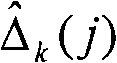
例如,在相位估算器110中,第k个时钟周期中的估算相位误差
在公式(2)中,项
一般的硬盘驱动器具有长度为4的信道。换句话说,在信道内有码间干扰(ISI)的地方,信号响应散布在多个采样位置上。具体地,长度为4的“1+2D+2D2+D3”部分响应(PR:partial response)信道在时间k产生响应‘1’,在时间k+1产生响应‘2’,在时间k+2产生响应‘2’,在时间k+3产生响应‘1’。信道的最终输出信号将是在不同时间生成的部分响应的和。Typical hard drives have channels of length 4. In other words, where there is intersymbol interference (ISI) within the channel, the signal response is spread over multiple sampling locations. Specifically, the “1+2D+2D 2 +D 3 ” partial response (PR: partial response) channel with a length of 4 produces a response '1' at time k, a response '2' at
导数信道是PR信道的时间连续形式表示的导数,因此它的长度通常大于PR信道长度。为了便于解释,将假定导数信道的长度为6。由此,假定二进制数据yk的长度为4,二进制数据εk的长度为6。然而,硬盘驱动器的信道长度可能随着硬盘驱动器记录密度的增加而增加。当硬盘驱动器的记录密度增加时,二进制数据yk和εk各自的长度也趋于增加。The derivative channel is the derivative of the time-continuous representation of the PR channel, so its length is usually larger than the PR channel length. For ease of explanation, it will be assumed that the length of the derivative channel is six. Thus, it is assumed that the length of the binary data y k is 4, and the length of the binary data ε k is 6. However, the channel length of a hard disk drive may increase as the recording density of the hard disk drive increases. When the recording density of a hard disk drive increases, the respective lengths of the binary data y k and ε k also tend to increase.
在公式(2)中,前一估算相位误差被用来计算当前的估算相位误差

另外,公式(2)的递归结构类似于分支度量计算或者路径度量计算,因此与维特比解码中使用的技术类似的技术可以被用于相位估算器110中。In addition, the recursive structure of formula (2) is similar to branch metric calculation or path metric calculation, so techniques similar to those used in Viterbi decoding can be used in
公式(2)中的项γ(ekεk-ek-Mεk-M)表示当前相位估算值ekεk和先前相位估算值ek-Mεk-M之间的差异与常数γ的乘积。使用先前相位估算值趋于减小相位误差计算中的噪声影响。公式(2)计算使通过M个样本的观察窗的ei=ci-yi和

可以通过根据估算相位误差的变化调整M的大小来调整跟踪性能。例如,通过监视估算的相位误差的变化,可以通过随着估算相位误差的变化而自动调整M的数值来调整跟踪性能。还可以调整M的数值,达到期望的噪声容限度和期望的系统性能之间的权衡。M值的该调整例如可以通过仿真来确定。Tracking performance can be tuned by adjusting the size of M according to changes in the estimated phase error. For example, by monitoring changes in the estimated phase error, tracking performance can be adjusted by automatically adjusting the value of M as the estimated phase error changes. The value of M can also be adjusted to achieve a trade-off between desired noise margin and desired system performance. This adjustment of the value of M can be determined, for example, by simulation.
γ的数值一般根据M值和导数信道的输出来确定,γ值的适当调整可以有助于减小在计算估算相位误差时的噪声影响。The value of γ is generally determined according to the M value and the output of the derivative channel, and proper adjustment of the γ value can help reduce the influence of noise when calculating and estimating the phase error.
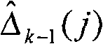
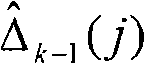
实现公式(2)的硬件一般需要存储M个先前相位误差估算值的结构。结果,硬件的复杂度随着M值的增加而增加。然而,硬件的复杂度可以通过调整公式(2)而获得下述公式(3)来降低:Hardware implementing equation (2) typically requires a structure to store M previous phase error estimates. As a result, the complexity of the hardware increases as the value of M increases. However, the hardware complexity can be reduced by adjusting formula (2) to obtain the following formula (3):
Δk=μΔk-1+γekεk. (3)Δ k = μΔ k-1 + γe k ε k . (3)
在公式(3)中,μ是根据M值确定的遗忘因子。遗忘因子μ可以用例如
图3是根据本发明又一实施例的信号再现设备的框图。FIG. 3 is a block diagram of a signal reproducing device according to still another embodiment of the present invention.
参看图3,该设备包括模数转换器(ADC)302、均衡器304、分支度量计算&相位补偿电路(BMC)306、相加比较选择&路径存储电路(ACS&PM)308、相位估算器310、环路滤波器312、数模转换器(DAC)314、以及压控振荡器(VCO)316。ACS&PM 308包括相加比较选择器(ACS)308a、数据路径存储器308b和相位路径存储器308c。Referring to FIG. 3, the device includes an analog-to-digital converter (ADC) 302, an
ADC 302接收与存储在诸如硬盘驱动器的磁盘之类的数据存储介质上的数据相关生成的输入信号,并对该信号采样。该输入信号一般通过硬盘驱动器的磁头来产生。ADC 302对输入信号进行采样,以产生已采样的输入信号,并且采样后的输入信号然后被均衡器304整形,以产生信号ck。
BMC 306通过向维特比网格结构或其它类似数据结构的每个分支施加对应的估算相位误差值来计算信号ck的分支度量。BMC 306可以使用的分支度量的示例是欧几里德距离。欧几里德距离的示例根据下述公式(4)提供:
在公式(4)中,是使用公式(2)或(3)获得的估算相位误差值。相对于不将估算相位误差

在图3中,索引“i”和“j”分别用来表示维特比网格结构中当前和下一状态。例如,在图4中,状态“i”和“j”从状态“11111”、“11110”、…、“00000”中选取。为了图示状态“i”和“j”的使用,项λ10(11111,01111)是“11111”和“01111”之间的分支在时间“k=10”时的分支度量。In FIG. 3, indices "i" and "j" are used to denote the current and next states in the Viterbi trellis structure, respectively. For example, in FIG. 4, states "i" and "j" are selected from states "11111", "11110", ..., "00000". To illustrate the use of states "i" and "j", the term λ 10 (11111, 01111) is the branch metric for the branch between "11111" and "01111" at time "k=10".
项yk(j)表示图4中的在时间“k”到状态“j”的理想信道输出。例如,y10(11111)是涉及从状态“11111”或“11110”到状态“11111”的两个分支在时间“k=10”时的理想信道输出。类似地,项ck(j)表示维特比网格结构中时间“k”和状态“j”时项ck的值。The term y k (j) represents the ideal channel output at time "k" to state "j" in FIG. 4 . For example, y 10 (11111) is the ideal channel output at time "k=10" involving two branches from state "11111" or "11110" to state "11111". Similarly, term c k (j) represents the value of term c k at time "k" and state "j" in the Viterbi trellis structure.
项εk(i,j)表示图4中从“i”到“j”的分支在时间“k”的导数信道输出。项


项
为了计算维特比网格结构的分支的分支度量λk,公式(4)可以表示为
ACS&PM 308根据BMC 306的输出来计算估算相位误差值
ACS&PM 308包括相位路径存储器308c,用于存储在维特比解码操作中使用的所有估算相位误差值ACS&PM 308在相位路径存储器308c中存储估算相位误差值并仅将与幸存路径对应的最佳估算相位误差输出到环路滤波器312。
下面将进一步详细描述ACS&PM 308的操作。The operation of the
图4示出了具有长度4的通信信道的维特比网格结构。相关的导数通信信道的信道长度为6。Figure 4 shows a Viterbi trellis structure with a communication channel of length 4. The associated derivative communication channel has a channel length of six.
相位估算器310根据图4图示的维特比网格结构、并且根据下面的公式(5)-(8)来计算yk(i)、εk(i,j)和

图4的维特比网格结构被应用到最常用的长度为4信道。与长度为4的信道对应的导数通信信道是长度为6信道。图4中状态值“i”和“j”的范围在0到31(二进制数值的00000~11111)之间。图4中,使用了5位状态作为示例,因为5位码字是许多当前数据存储应用中最常用的。The Viterbi trellis structure of Fig. 4 is applied to the most commonly used channel of length 4. The derivative communication channel corresponding to a channel of length 4 is a channel of
项yk(i)、εk(i,j)和
在公式(5)中,“k”表示当前时间,项
项εk(i,j)可以用下述公式(6)计算得到:The term ε k (i, j) can be calculated by the following formula (6):
项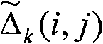
公式(7)和(8)中的误差项e(i,j)可以用下述公式(9)计算得到:The error term e(i, j) in formulas (7) and (8) can be calculated by the following formula (9):
ek(i,j)=ck-yk(i) (9)e k (i, j) = c k -y k (i) (9)
BMC 306使用相位估算器310输出的yk(i)、εk(i,j)和
然后,BMC 306将λk(i,j)发送到具有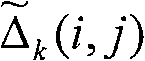
ACS 308a使用BMC 306输出的λk(i,j)和
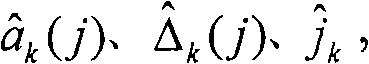
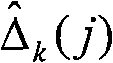


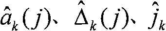
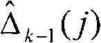
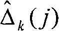
数据路径存储器308b用从ACS 308a发送的根据下列公式(16)和(17)以及图4所示的维特比网格结构,来更新用于数据估算的L长度的路径存储值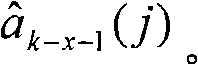
同时,相位路径存储器308c用从ACS 308a发送的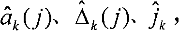

这里,‘L’和‘P’分别优化用于数据估算和相位估算。Here, 'L' and 'P' are optimized for data estimation and phase estimation, respectively.
图5示出了用于数据估算的长度为L的数据路径存储器308b的示意结构,其根据图4所示的维特比网格结构而构造。数据路径存储器308b确定最佳的数据估算值

图6示出了用于相位估算的长度P的相位路径存储器308c的示意结构,其根据图4所示的维特比网格结构而构造。相位路径存储器308c确定最佳相位估算值

另外,ACS&PM 308将在先前周期输入到相位存储器308c的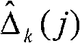
均用于计算估算相位误差的公式(2)和(14)的相似点在于它们都具有递归结构。另外,因为相位估算的方式与数据估算类似,所以基于图4所示的维特比网格结构来计算多个smk(j)和 Equations (2) and (14), both of which are used to calculate the estimated phase error, are similar in that they both have a recursive structure. In addition, because the phase estimation method is similar to the data estimation, multiple sm k (j) and
图5所示的数据路径存储器308b将二进制数据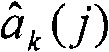
同时,图6所示的相位路径存储器308c将浮点数据

选择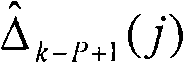


本发明的所选实施例中,与维特比解码器的路径度量计算公式相似,具有递归结构的公式被用来计算相位误差

最后,使用路径存储器,以与维特比解码器执行数据检测类似的方式,来执行一个相位误差的确定。Finally, using the path memory, a phase error ok.
信道特性fk一般根据系统决定,而导数信道特性gk通过对信道特性fk求微分而获得。因此,如果信道特性fk已知,则导数信道特性gk也可以很容易获得。The channel characteristic f k is generally determined according to the system, and the derivative channel characteristic g k is obtained by differentiating the channel characteristic f k . Therefore, if the channel characteristic fk is known, the derivative channel characteristic gk can also be obtained easily.
通常,当脉冲响应fk被求微分时,表示脉冲响应的特性值增加。例如,在一个示例中,硬盘驱动器的信道长度是4,但是通过将长度为4的信道微分获得的信道的长度是6。维特比解码器中的状态数量由信道的长度确定,对于长度为4的信道,其状态数量是24=16,而长度为6的导数信道的状态数量是26=64。如果根据长度较长的导数信道确定状态数量,则自然考虑到了长度较短的信道的全部状态。In general, when the impulse response f k is differentiated, the characteristic value representing the impulse response increases. For example, in one example, the channel length of the hard disk drive is 4, but the length of the channel obtained by differentiating the channel of length 4 is 6. The number of states in a Viterbi decoder is determined by the length of the channel, which is 2 4 =16 for a channel of
然而,在其他情况下,例如根据长度较短的信道来确定状态数量,就不能考虑到长度较长的导数信道的全部状态。However, in other cases, such as determining the number of states from a channel of shorter length, not all states of the derivative channel of longer length can be considered.
由此,维特比解码所需的状态数量应该根据在信道或导数信道之中脉冲响应长度较长的信道来确定。从而可以考虑到所有可能的情况。Therefore, the number of states required for Viterbi decoding should be determined according to a channel having a longer impulse response length among channels or derivative channels. All possible situations can thus be considered.
相位估算器310通过查看ACS&PM 308的数据估算值来计算相位估算值,并将相位估算值提供给BMC 306。
这里,最后的相位估算值和数据估算值是由基于在BMC 306中计算的分支度量值确定的幸存路径值和先前计算的状态度量值来确定的。这样做增强了估算可靠性。Here, the final phase estimate and data estimate are determined from survivor path values determined based on branch metrics computed in
而且,ACS&PM 308的最后相位估算值被提供给环路滤波器312。Also, the final phase estimate of
环路滤波器112生成与ACS&PM 308所提供的相位估算值对应的控制信号。DAC 314将该控制信号转换成模拟控制信号,并且所述模拟控制信号改变VCO 316的振荡频率。
因为ADC 302与VCO 316生成的时钟信号同步地执行采样操作,所以可以通过控制VCO 316的振荡频率来补偿定时误差。Since the
在确定相位误差时,图3的设备不仅使用当前信号,而且使用所有往昔的信号,从而可以以更高的可靠性进行确定。When determining the phase error, the device of FIG. 3 uses not only the current signal, but also all past signals, so that the determination can be made with higher reliability.
另外,即使在相位估算中,图3的设备也可以通过使用与维特比解码器的数据估算相同的方法来增加可靠性。具体地,联合使用数据估算结果和相位估算结果,从而可以进一步增强估算的可靠性。In addition, even in phase estimation, the apparatus of FIG. 3 can increase reliability by using the same method as the data estimation of the Viterbi decoder. Specifically, the data estimation result and the phase estimation result are used jointly, so that the reliability of the estimation can be further enhanced.
图7A和7B是示出了定时误差的平均值的仿真结果的示意图。具体地,图7A示出了使用包括最小均方差误差(MMSE)估算的传统方法测量的定时误差的平均值,图7B示出了使用本发明实施例的包括相位估算最大似然(PEML)的方法测量的定时误差的平均值。在图7A和7B中,x轴表示实际归一化后的定时误差,y轴表示测量的平均定时误差。因此,理想的定时误差估算器将生成图7A和7B中的直线。7A and 7B are diagrams showing simulation results of average values of timing errors. Specifically, FIG. 7A shows the average of timing errors measured using conventional methods including minimum mean square error (MMSE) estimation, and FIG. The average of the timing errors measured by the method. In Figures 7A and 7B, the x-axis represents the actual normalized timing error and the y-axis represents the measured average timing error. Therefore, an ideal timing error estimator would generate the straight lines in Figures 7A and 7B.
在图7和8二者中,标记“6dB~18dB”表示已经进行误差估算的信号的信噪比(SNR)。SNR用分贝(dB)标度表示。图7和8中的“定时误差”是归一化后的相位误差,其中“-0.5”对应于相位“-π”,“+0.5”对应于相位“+π”。在环路滤波器312的输入端仿真测量定时误差。在图7和8表示的每次仿真中,环路滤波器312的输出端被设置为表示恒定的相位误差。In both FIGS. 7 and 8 , the notation "6dB∼18dB" indicates the signal-to-noise ratio (SNR) of the signal for which error estimation has been performed. SNR is expressed on a decibel (dB) scale. "Timing Error" in Figures 7 and 8 is the normalized phase error, where "-0.5" corresponds to the phase "-π", and "+0.5" corresponds to the phase "+π". The timing error is simulated at the input of the
图8A和8B是分别示出了使用传统MMSE方法和根据本发明实施例的PEML方法测量的定时误差变化的仿真结果的图。图8A和8B中的变化是根据图7A和7B所示的平均值来测量的。在图8A和8B中,可以看出,使用本发明的实施例中的方法改善了变化。8A and 8B are graphs showing simulation results of timing error changes measured using the conventional MMSE method and the PEML method according to an embodiment of the present invention, respectively. The changes in Figures 8A and 8B were measured from the average values shown in Figures 7A and 7B. In Figures 8A and 8B, it can be seen that the variation is improved using the method in an embodiment of the present invention.
图9A和9B示出了跟踪性能的仿真结果。图9A图示了传统MMSE方法的跟踪性能,而图9B图示了根据本发明实施例的PEML方法的跟踪性能。一般来说,跟踪性能可以用两个因素评估。首先根据跟踪性能收敛到目标值的速度、其次根据跟踪曲线的波动幅度来评价跟踪性能。图9A和9B中,跟踪曲线几乎同时收敛到目标值,但是当使用传统方法时,波动很严重。图9A中的波动将导致定时环路中的较差的抖动性能。9A and 9B show simulation results of tracking performance. FIG. 9A illustrates the tracking performance of the conventional MMSE method, while FIG. 9B illustrates the tracking performance of the PEML method according to an embodiment of the present invention. In general, tracking performance can be evaluated by two factors. Firstly, the tracking performance is evaluated according to the speed at which the tracking performance converges to the target value, and secondly, according to the fluctuation range of the tracking curve. In Figures 9A and 9B, the tracking curves converge to the target value almost simultaneously, but when using the conventional method, the fluctuations are severe. The fluctuations in Figure 9A will result in poor jitter performance in the timing loop.
图10是示出了稳态抖动性能的仿真结果的图。在图10中,标记为MMSE的曲线图示了传统方法的稳态抖动性能,而标记为PEML的曲线图示了根据本发明实施例的方法的稳态抖动性能。在图10中,可以看出,根据本发明实施例的方法的抖动性能比传统方法的抖动性能更好。FIG. 10 is a graph showing simulation results of steady-state jitter performance. In FIG. 10 , the curve labeled MMSE illustrates the steady-state jitter performance of the conventional method, while the curve labeled PEML illustrates the steady-state jitter performance of the method according to an embodiment of the present invention. In FIG. 10 , it can be seen that the jitter performance of the method according to the embodiment of the present invention is better than that of the conventional method.
图11是根据本发明实施例的方法相对于传统方法在几个不同的参数上的改进的示意图。Fig. 11 is a schematic diagram of the improvement of the method according to the embodiment of the present invention on several different parameters relative to the traditional method.
参看图11,相对于传统方法,本发明的实施例改进了跟踪性能、捕捉范围、以及抖动性能。另一方面,计算速度和硬件效率稍微降低。然而,这些缺陷经常由于跟踪、捕捉范围和抖动性能的改进而超限。Referring to FIG. 11 , embodiments of the present invention improve tracking performance, capture range, and jitter performance relative to conventional methods. On the other hand, computational speed and hardware efficiency are slightly reduced. However, these deficiencies are often overridden by improvements in tracking, capture range, and jitter performance.
通过使用图3所示的上述设备,即使在由于高密度数据存储而导致再现信号质量很差的环境中,也可以执行相位估算。另外,使能信号定时的稳定恢复,并增强了数据记录密度。此外,诸如结合图3描述的上述设备防止在以高密度记录信号时相位同步环路中的错误操作,并且减小了定时抖动导致的噪声。By using the above-described apparatus shown in FIG. 3, phase estimation can be performed even in an environment where the reproduced signal quality is poor due to high-density data storage. In addition, stable recovery of signal timing is enabled, and data recording density is enhanced. Furthermore, an apparatus such as that described above in connection with FIG. 3 prevents erroneous operation in a phase synchronization loop when recording signals at high density, and reduces noise caused by timing jitter.
上述优选实施例只是示范性示例。本领域的普通技术人员应该明白,可以对优选实施例进行形式和细节上的各种改变,而不会偏离由所附权利要求书限定的本发明的范围。The preferred embodiments described above are illustrative examples only. It will be understood by those of ordinary skill in the art that various changes in form and details may be made in the preferred embodiment without departing from the scope of the invention as defined in the appended claims.
Claims (22)
Applications Claiming Priority (2)
| Application Number | Priority Date | Filing Date | Title |
|---|---|---|---|
| US11/598,807 US7889818B2 (en) | 2006-11-14 | 2006-11-14 | Method and apparatus for controlling sampling of signals produced in relation to stored data |
| US11/598,807 | 2006-11-14 |
Publications (2)
| Publication Number | Publication Date |
|---|---|
| CN101286322A true CN101286322A (en) | 2008-10-15 |
| CN101286322B CN101286322B (en) | 2012-04-18 |
Family
ID=39092798
Family Applications (1)
| Application Number | Title | Priority Date | Filing Date |
|---|---|---|---|
| CN2007103051096A Expired - Fee Related CN101286322B (en) | 2006-11-14 | 2007-11-14 | Method and apparatus for controlling sampling of signals produced in relation to stored data |
Country Status (4)
| Country | Link |
|---|---|
| US (1) | US7889818B2 (en) |
| EP (1) | EP1923884A3 (en) |
| KR (1) | KR100896187B1 (en) |
| CN (1) | CN101286322B (en) |
Cited By (1)
| Publication number | Priority date | Publication date | Assignee | Title |
|---|---|---|---|---|
| WO2011107006A1 (en) * | 2010-03-05 | 2011-09-09 | 中兴通讯股份有限公司 | Signal processing system and method |
Families Citing this family (3)
| Publication number | Priority date | Publication date | Assignee | Title |
|---|---|---|---|---|
| US8737542B1 (en) | 2010-01-12 | 2014-05-27 | Marvell International Ltd. | Method and apparatus for data reception in high-speed applications |
| US8665941B1 (en) * | 2012-06-20 | 2014-03-04 | MagnaCom Ltd. | Decision feedback equalizer for highly spectrally efficient communications |
| US9312875B1 (en) * | 2015-06-26 | 2016-04-12 | Intel IP Corporation | Signal processing apparatus and method for processing a signal |
Family Cites Families (15)
| Publication number | Priority date | Publication date | Assignee | Title |
|---|---|---|---|---|
| US5303263A (en) * | 1991-06-25 | 1994-04-12 | Oki Electric Industry Co., Ltd. | Transmission channel characteristic equalizer |
| US5216554A (en) * | 1991-07-01 | 1993-06-01 | International Business Machines Corporation | Digital phase error estimator |
| KR100355391B1 (en) * | 1995-10-10 | 2002-12-18 | 삼성전자 주식회사 | Data pattern adaptive clock restoration method and apparatus |
| US5940450A (en) * | 1997-02-28 | 1999-08-17 | Hitachi America, Ltd. | Carrier recovery method and apparatus |
| JP2985957B1 (en) * | 1998-09-11 | 1999-12-06 | 松下電器産業株式会社 | Phase comparator and digital phase locked loop |
| US20030152175A1 (en) * | 1999-01-13 | 2003-08-14 | Ryohei Kuki | Post-processor using a noise whitened matched filter for a mass data storage device, or the like |
| US6650699B1 (en) * | 1999-01-21 | 2003-11-18 | International Business Machines Corporation | Methods and apparatus for timing recovery from a sampled and equalized data signal |
| US6914948B2 (en) * | 1999-03-22 | 2005-07-05 | Texas Instruments Incorporated | Media noise post-processor with varying threshold |
| US6460150B1 (en) | 2000-03-02 | 2002-10-01 | International Business Machines Corporation | Noise-predictive post-processing for PRML data channel |
| US6791776B2 (en) * | 2000-04-26 | 2004-09-14 | Hitachi, Ltd. | Apparatus for information recording and reproducing |
| US6581182B1 (en) * | 2000-05-15 | 2003-06-17 | Agere Systems Inc. | Iterative decoding with post-processing of detected encoded data |
| US6738206B2 (en) * | 2000-11-24 | 2004-05-18 | Texas Instruments Incorporated | Decision error compensation technique for decision-directed timing recovery loop |
| US6931585B1 (en) * | 2002-01-03 | 2005-08-16 | Marvell International Ltd. | Detection in the presence of media noise |
| JP4006294B2 (en) * | 2002-08-07 | 2007-11-14 | 富士通株式会社 | Timing recovery method and storage device |
| JP2005135532A (en) * | 2003-10-30 | 2005-05-26 | Sony Corp | Adaptive equalization apparatus, decoding apparatus, and error detection apparatus |
-
2006
- 2006-11-14 US US11/598,807 patent/US7889818B2/en not_active Expired - Fee Related
-
2007
- 2007-04-27 KR KR1020070041586A patent/KR100896187B1/en not_active Expired - Fee Related
- 2007-11-13 EP EP07120572.8A patent/EP1923884A3/en not_active Withdrawn
- 2007-11-14 CN CN2007103051096A patent/CN101286322B/en not_active Expired - Fee Related
Cited By (1)
| Publication number | Priority date | Publication date | Assignee | Title |
|---|---|---|---|---|
| WO2011107006A1 (en) * | 2010-03-05 | 2011-09-09 | 中兴通讯股份有限公司 | Signal processing system and method |
Also Published As
| Publication number | Publication date |
|---|---|
| CN101286322B (en) | 2012-04-18 |
| KR100896187B1 (en) | 2009-05-12 |
| KR20080043681A (en) | 2008-05-19 |
| US20080112513A1 (en) | 2008-05-15 |
| US7889818B2 (en) | 2011-02-15 |
| EP1923884A2 (en) | 2008-05-21 |
| EP1923884A3 (en) | 2014-04-02 |
Similar Documents
| Publication | Publication Date | Title |
|---|---|---|
| US7002767B2 (en) | Detection of recorded data employing interpolation with gain compensation | |
| US6912099B2 (en) | Maximum likelihood detection of asynchronous servo data employing interpolation | |
| US6246723B1 (en) | Sampled amplitude read channel employing early-decisions from a trellis sequence detector for sampling value estimation | |
| US7551668B2 (en) | Adaptive equalizing apparatus and method | |
| US20050135472A1 (en) | Adaptive equalizer, decoding device, and error detecting device | |
| US7564931B2 (en) | Robust maximum-likelihood based timing recovery | |
| JP2005276412A (en) | Apparatus for dynamic equalizer optimization | |
| US20050169412A1 (en) | Pattern-dependent equalization and detection | |
| US6791776B2 (en) | Apparatus for information recording and reproducing | |
| US20110002375A1 (en) | Information reproducing apparatus using adaptive equalizer and adaptive equalization method | |
| US20050219727A1 (en) | Signal processing device and signal processing method | |
| JP4008677B2 (en) | Information recording / reproducing apparatus, signal decoding circuit, recording structure and method of information recording medium | |
| US7545862B2 (en) | Adaptive equalizer, decoding device, and error detecting device | |
| JP2003085764A (en) | Waveform equalizer and PRML detector | |
| US7113555B2 (en) | Data channel with joint data estimation and timing recovery | |
| CN101286322B (en) | Method and apparatus for controlling sampling of signals produced in relation to stored data | |
| US7561640B2 (en) | Method and apparatus for interative noise whitening with causal and anti-causal prediction filters | |
| JP3776582B2 (en) | Recording / playback device | |
| US7978792B2 (en) | Reproducing apparatus and method, signal processing apparatus and method, and program | |
| Patapoutian | Baseline wander compensation for the perpendicular magnetic recording channel | |
| JP4727310B2 (en) | Waveform equalization apparatus, information reproducing apparatus, waveform equalization method, waveform equalization program, and recording medium | |
| JP3994987B2 (en) | Playback device | |
| JP3875154B2 (en) | Waveform equalization apparatus, information reproducing apparatus, communication apparatus, waveform equalization method, waveform equalization program, and computer-readable recording medium recording the waveform equalization program | |
| JP5579379B2 (en) | Frequency error combinational logic configured for a multi-channel data detection system and method for generating frequency errors | |
| JP5579380B2 (en) | Error combination logic configured for a multi-channel data detection system and method for generating an error signal |
Legal Events
| Date | Code | Title | Description |
|---|---|---|---|
| C06 | Publication | ||
| PB01 | Publication | ||
| C10 | Entry into substantive examination | ||
| SE01 | Entry into force of request for substantive examination | ||
| C14 | Grant of patent or utility model | ||
| GR01 | Patent grant | ||
| CF01 | Termination of patent right due to non-payment of annual fee |
Granted publication date: 20120418 Termination date: 20141114 |
|
| EXPY | Termination of patent right or utility model |