CN101275219A - Organosilane compounds used to modify the dielectric properties of silicon oxide and silicon nitride films - Google Patents
Organosilane compounds used to modify the dielectric properties of silicon oxide and silicon nitride films Download PDFInfo
- Publication number
- CN101275219A CN101275219A CNA200710306176XA CN200710306176A CN101275219A CN 101275219 A CN101275219 A CN 101275219A CN A200710306176X A CNA200710306176X A CN A200710306176XA CN 200710306176 A CN200710306176 A CN 200710306176A CN 101275219 A CN101275219 A CN 101275219A
- Authority
- CN
- China
- Prior art keywords
- carbon
- precursor
- depositing
- film
- silicon nitride
- Prior art date
- Legal status (The legal status is an assumption and is not a legal conclusion. Google has not performed a legal analysis and makes no representation as to the accuracy of the status listed.)
- Granted
Links
Images


Classifications
-
- C—CHEMISTRY; METALLURGY
- C23—COATING METALLIC MATERIAL; COATING MATERIAL WITH METALLIC MATERIAL; CHEMICAL SURFACE TREATMENT; DIFFUSION TREATMENT OF METALLIC MATERIAL; COATING BY VACUUM EVAPORATION, BY SPUTTERING, BY ION IMPLANTATION OR BY CHEMICAL VAPOUR DEPOSITION, IN GENERAL; INHIBITING CORROSION OF METALLIC MATERIAL OR INCRUSTATION IN GENERAL
- C23C—COATING METALLIC MATERIAL; COATING MATERIAL WITH METALLIC MATERIAL; SURFACE TREATMENT OF METALLIC MATERIAL BY DIFFUSION INTO THE SURFACE, BY CHEMICAL CONVERSION OR SUBSTITUTION; COATING BY VACUUM EVAPORATION, BY SPUTTERING, BY ION IMPLANTATION OR BY CHEMICAL VAPOUR DEPOSITION, IN GENERAL
- C23C16/00—Chemical coating by decomposition of gaseous compounds, without leaving reaction products of surface material in the coating, i.e. chemical vapour deposition [CVD] processes
- C23C16/22—Chemical coating by decomposition of gaseous compounds, without leaving reaction products of surface material in the coating, i.e. chemical vapour deposition [CVD] processes characterised by the deposition of inorganic material, other than metallic material
- C23C16/30—Deposition of compounds, mixtures or solid solutions, e.g. borides, carbides, nitrides
- C23C16/42—Silicides
-
- C—CHEMISTRY; METALLURGY
- C23—COATING METALLIC MATERIAL; COATING MATERIAL WITH METALLIC MATERIAL; CHEMICAL SURFACE TREATMENT; DIFFUSION TREATMENT OF METALLIC MATERIAL; COATING BY VACUUM EVAPORATION, BY SPUTTERING, BY ION IMPLANTATION OR BY CHEMICAL VAPOUR DEPOSITION, IN GENERAL; INHIBITING CORROSION OF METALLIC MATERIAL OR INCRUSTATION IN GENERAL
- C23C—COATING METALLIC MATERIAL; COATING MATERIAL WITH METALLIC MATERIAL; SURFACE TREATMENT OF METALLIC MATERIAL BY DIFFUSION INTO THE SURFACE, BY CHEMICAL CONVERSION OR SUBSTITUTION; COATING BY VACUUM EVAPORATION, BY SPUTTERING, BY ION IMPLANTATION OR BY CHEMICAL VAPOUR DEPOSITION, IN GENERAL
- C23C16/00—Chemical coating by decomposition of gaseous compounds, without leaving reaction products of surface material in the coating, i.e. chemical vapour deposition [CVD] processes
- C23C16/22—Chemical coating by decomposition of gaseous compounds, without leaving reaction products of surface material in the coating, i.e. chemical vapour deposition [CVD] processes characterised by the deposition of inorganic material, other than metallic material
- C23C16/30—Deposition of compounds, mixtures or solid solutions, e.g. borides, carbides, nitrides
- C23C16/34—Nitrides
- C23C16/345—Silicon nitride
-
- C—CHEMISTRY; METALLURGY
- C23—COATING METALLIC MATERIAL; COATING MATERIAL WITH METALLIC MATERIAL; CHEMICAL SURFACE TREATMENT; DIFFUSION TREATMENT OF METALLIC MATERIAL; COATING BY VACUUM EVAPORATION, BY SPUTTERING, BY ION IMPLANTATION OR BY CHEMICAL VAPOUR DEPOSITION, IN GENERAL; INHIBITING CORROSION OF METALLIC MATERIAL OR INCRUSTATION IN GENERAL
- C23C—COATING METALLIC MATERIAL; COATING MATERIAL WITH METALLIC MATERIAL; SURFACE TREATMENT OF METALLIC MATERIAL BY DIFFUSION INTO THE SURFACE, BY CHEMICAL CONVERSION OR SUBSTITUTION; COATING BY VACUUM EVAPORATION, BY SPUTTERING, BY ION IMPLANTATION OR BY CHEMICAL VAPOUR DEPOSITION, IN GENERAL
- C23C16/00—Chemical coating by decomposition of gaseous compounds, without leaving reaction products of surface material in the coating, i.e. chemical vapour deposition [CVD] processes
- C23C16/22—Chemical coating by decomposition of gaseous compounds, without leaving reaction products of surface material in the coating, i.e. chemical vapour deposition [CVD] processes characterised by the deposition of inorganic material, other than metallic material
- C23C16/30—Deposition of compounds, mixtures or solid solutions, e.g. borides, carbides, nitrides
- C23C16/40—Oxides
- C23C16/401—Oxides containing silicon
-
- H10P14/20—
-
- H10P14/69215—
-
- H10P14/6334—
-
- H10P14/6336—
-
- H10P14/6682—
-
- H10P14/6922—
-
- H10P14/69433—
Landscapes
- Chemical & Material Sciences (AREA)
- General Chemical & Material Sciences (AREA)
- Chemical Kinetics & Catalysis (AREA)
- Engineering & Computer Science (AREA)
- Materials Engineering (AREA)
- Mechanical Engineering (AREA)
- Metallurgy (AREA)
- Organic Chemistry (AREA)
- Inorganic Chemistry (AREA)
- Formation Of Insulating Films (AREA)
- Chemical Vapour Deposition (AREA)
Abstract
Description
相关申请的对照参考Cross References to Related Applications
[0001]本申请要求申请号为No.60/861,327、申请日为2006年11月28日的美国临时申请的权益。该临时申请的公开内容并入本文作为参考。[0001] The application requires that the application number be No.60/861,327, and the date of application is the benefit of the U.S. Provisional Application on November 28, 2006. The disclosure of this provisional application is incorporated herein by reference.
背景技术 Background technique
[0002]在用于集成电路的晶体管结构的制造过程中,氧化硅膜被用于各种各样的应用。这些应用包括用作用于离子注入的硬掩模,控制接触孔洞蚀刻的蚀刻阻挡物、沿着栅设置的侧壁分割膜、用来屏蔽相邻物质以免受刻蚀或清洁过程破坏的保护膜、环境阻挡层、和减少外部边缘电容的介电物质。为了解决这些许多的需求,定制这些膜的化学和物理性质是必需的。[0002] Silicon oxide films are used in a variety of applications in the fabrication of transistor structures for integrated circuits. These applications include use as hardmasks for ion implantation, etch stops to control contact hole etching, sidewall partition films along gates, protective films to shield adjacent species from etching or cleaning processes, Environmental barriers, and dielectric substances to reduce external fringe capacitance. To address these many demands, tailoring the chemical and physical properties of these membranes is necessary.
[0003]用于制备氧化硅和氮化硅的较低温度的方法已通过采用化学前体而被发展起来,所述前体例如是六氯乙硅烷(HCDS)、二叔丁基硅烷(BTBAS)和二乙基硅烷(LTO-410)。然而,可用来改变由这些化学物质制备出的膜的性质的方法灵活性却非常小,所述性质例如介电常数、密度、湿法蚀刻速率。[0003] Lower temperature methods for the preparation of silicon oxide and silicon nitride have been developed using chemical precursors such as hexachlorodisilane (HCDS), di-tert-butylsilane (BTBAS ) and diethylsilane (LTO-410). However, there is very little flexibility in the methods available to alter the properties of films produced from these chemistries, such as dielectric constant, density, wet etch rate.
[0004]美国专利申请2006/0228903A1教导了采用两种前体化学物质的组合来制造碳掺杂的氮化硅膜。前体1被用于制造膜结构,前体2被用于添加碳到膜中。公开的内容包含了结构形成性前体例如BTBAS、二氯硅烷(DCS)、HCDS、以及其它的氨基硅烷。许多烷基硅烷前体被确定用作碳掺杂前体。这些前体包含甲基硅烷(1MS)、二甲基硅烷(2MS)、三甲基硅烷(3MS)、和四甲基硅烷(4MS)。另外,其它确定的前体族系包括烷基乙硅烷(alkyldisilane)和包含卤素的烷基硅烷。尽管该专利申请确定了各种各样的潜在添加物,却没有实验数据来验证其方法的可行性。例如,已知一些连接于硅上的烷基的键裂解能是非常弱的,并且,因此,不能被结合到所沉积的膜中。[0004] US Patent Application 2006/0228903A1 teaches the use of a combination of two precursor chemistries to fabricate carbon-doped silicon nitride films. Precursor 1 was used to fabricate the membrane structure and Precursor 2 was used to add carbon to the membrane. The disclosure includes structure-forming precursors such as BTBAS, dichlorosilane (DCS), HCDS, and other aminosilanes. A number of alkylsilane precursors have been identified as carbon doping precursors. These precursors include methylsilane (1MS), dimethylsilane (2MS), trimethylsilane (3MS), and tetramethylsilane (4MS). Additionally, other identified precursor families include alkyldisilanes and halogen-containing alkylsilanes. Although the patent application identifies a wide variety of potential additives, there is no experimental data to verify the feasibility of its approach. For example, some silicon-attached alkyl groups are known to have very weak bond cleavage energies and, therefore, cannot be incorporated into the deposited film.
[0005]美国专利申请2005/0236694A1教导了采用3MS和4MS通过等离子增强的化学气相沉积(PECVD)来沉积碳蚀刻阻挡(CES)膜。通过这个方法可沉积出在低于500℃的温度下具有变化的介电常数的碳掺杂的氧化硅和碳掺杂的氮化硅。PECVD是非常有效的沉积较低温度具有变化性质的物质的方法。然而,它不是非常有利的沉积非常接近于晶体管的膜的方法。[0005] US Patent Application 2005/0236694A1 teaches the deposition of carbon etch stop (CES) films by plasma enhanced chemical vapor deposition (PECVD) using 3MS and 4MS. Carbon-doped silicon oxide and carbon-doped silicon nitride with varying dielectric constants at temperatures below 500° C. can be deposited by this method. PECVD is a very efficient method of depositing lower temperature species with varying properties. However, it is not a very favorable method of depositing films very close to transistors.
[0006]美国专利2005/0255714A1教导了采用氨基乙硅烷、甲硅烷基氮化物、和甲硅烷基肼,通过低压化学气相沉积(LPCVD)来沉积氮化硅和氧化硅。尽管该申请提出了这些前体的可行性,却没有提供支持可以以一种解决制造集成电路中所需要利用的所有权成本(cost-of-ownership)的方式从这些前体制备出膜的实验数据。此外,可能存在涉及到安全操作和物质使用的问题。[0006] US Patent 2005/0255714A1 teaches the deposition of silicon nitride and silicon oxide by low pressure chemical vapor deposition (LPCVD) using aminodisilane, silyl nitride, and silylhydrazine. Although the application suggests the feasibility of these precursors, it does not provide experimental data to support that films can be prepared from these precursors in a manner that addresses the cost-of-ownership that needs to be exploited in the manufacture of integrated circuits . Additionally, there may be issues related to safe handling and use of the substance.
发明内容 Contents of the invention
[0007]本发明的一个实施方案是沉积具有提高的耐蚀刻性的包含碳的氧化硅膜或者包含碳的氮化硅膜的方法,该方法包括:One embodiment of the present invention is a method of depositing a carbon-containing silicon oxide film or a carbon-containing silicon nitride film having improved etch resistance, the method comprising:
提供包含硅的结构前体;providing a structural precursor comprising silicon;
提供包含碳的掺杂剂前体;providing a dopant precursor comprising carbon;
将包含碳的掺杂剂前体和包含硅的结构前体混合,以得到具有混合比率Rm(掺杂剂前体在混合物中的重量百分数)在2%和85%之间和流动速率Fm的混合物;The carbon-containing dopant precursor and the silicon-containing structure precursor are mixed to obtain a mixing ratio Rm (weight percent of the dopant precursor in the mixture) between 2% and 85% and a flow rate Fm. mixture;
提供具有流动速率Fc的化学改性剂;providing a chemical modifier with a flow rate Fc;
具有在25%和75%之间的流动比率R2,定义R2为R2=Fm/Fc;和having a flow ratio R2 between 25% and 75%, defining R2 as R2=Fm/Fc; and
制备具有提高的耐蚀刻性的包含碳的氧化硅膜或者包含碳的氮化硅膜,其中耐蚀刻性随着增加碳的结合而提高。A carbon-containing silicon oxide film or a carbon-containing silicon nitride film having improved etching resistance, wherein the etching resistance increases with increasing incorporation of carbon, is produced.
[0008]为了增加碳的结合,提高混合比率Rm。通过提高混合比率Rm,提高了耐蚀刻性。通过提高流动比率R2而进一步提高耐蚀刻性。通过提高混合比率Rm来提高沉积速率,并且通过提高流动比率R2来进一步提高沉积速率。通过提高混合比率Rm来降低膜密度,并且可通过提高流动比率R2来进一步提高膜密度。[0008] In order to increase the bonding of carbon, the mixing ratio Rm is increased. Etching resistance is improved by increasing the mixing ratio Rm. Etching resistance is further improved by increasing the flow ratio R2. The deposition rate is increased by increasing the mixing ratio Rm, and the deposition rate is further increased by increasing the flow ratio R2. The film density is lowered by increasing the mixing ratio Rm, and can be further increased by increasing the flow ratio R2.
[0009]沉积的方法在350℃和700℃之间的温度和在0.2托和10托之间的压力下进行。[0009] The method of deposition is carried out at a temperature between 350°C and 700°C and at a pressure between 0.2 Torr and 10 Torr.
[0010]沉积方法选自原子层沉积(ALD)、化学气相沉积(CVD)、低压化学气相沉积(LPCVD)、等离子增强的化学气相沉积(PECVD)和远程下游方法(RemoteDownstream Processes)。The deposition method is selected from atomic layer deposition (ALD), chemical vapor deposition (CVD), low pressure chemical vapor deposition (LPCVD), plasma enhanced chemical vapor deposition (PECVD) and remote downstream processes (RemoteDownstream Processes).
[0011]化学改性剂选自氧、氮、氨、氦、氩、氙、氢和其混合物。包含硅的结构前体选自二(叔丁基)硅烷(bis(tertiarybutyl)silane)、原硅酸四乙酯、二氯硅烷、六氯乙硅烷、甲基硅烷、二甲基硅烷、三甲基硅烷、四甲基硅烷、四乙烯基硅烷、苯基硅烷、环己基硅烷和其混合物。[0011] The chemical modifier is selected from oxygen, nitrogen, ammonia, helium, argon, xenon, hydrogen, and mixtures thereof. Silicon-containing structural precursors selected from bis(tertiarybutyl)silane, tetraethyl orthosilicate, dichlorosilane, hexachlorodisilane, methylsilane, dimethylsilane, trimethylsilane phenylsilane, tetramethylsilane, tetravinylsilane, phenylsilane, cyclohexylsilane and mixtures thereof.
[0012]本发明的另一个实施方案是用来沉积具有提高的耐蚀刻性的包含碳的氧化硅膜或者包含碳的氮化硅膜的低压化学气相沉积(LPCVD)方法,该方法包括:Another embodiment of the present invention is a low-pressure chemical vapor deposition (LPCVD) method for depositing a carbon-containing silicon oxide film or a carbon-containing silicon nitride film having improved etch resistance, the method comprising:
提供二(叔丁基)硅烷前体;providing a di(tert-butyl)silane precursor;
提供苯基硅烷前体;Provides phenylsilane precursors;
将苯基硅烷前体和二(叔丁基)硅烷前体混合,以得到具有混合比率Rm(添加到二(叔丁基)硅烷前体中的苯基硅烷前体重量百分数)在2%和85%之间和流动速率Fm的混合物;The phenylsilane precursor and the di(tert-butyl)silane precursor are mixed so as to have a mixing ratio Rm (the weight percentage of the phenylsilane precursor added to the di(tert-butyl)silane precursor) between 2% and Mixture between 85% and flow rate Fm;
提供化学改性剂,其选自氧、氮、氨和其混合物;且具有流动速率Fc;providing a chemical modifier selected from the group consisting of oxygen, nitrogen, ammonia, and mixtures thereof; and having a flow rate Fc;
具有在25%和75%之间的流动比率R2,定义R2为R2=Fm/Fc;和having a flow ratio R2 between 25% and 75%, defining R2 as R2=Fm/Fc; and
制备具有提高的耐蚀刻性的包含碳的氧化硅膜或者包含碳的氮化硅膜,其中耐蚀刻性随着增加碳的结合而提高。A carbon-containing silicon oxide film or a carbon-containing silicon nitride film having improved etching resistance, wherein the etching resistance increases with increasing incorporation of carbon, is produced.
[0013]为了增加碳的结合,提高混合比率Rm。通过提高混合比率Rm而提高耐蚀刻性。通过提高流动比率R2而进一步提高耐蚀刻性。通过提高混合比率Rm来提高沉积速率,并且通过提高流动比率R2来进一步提高沉积速率。通过提高混合比率Rm来降低膜密度,并且通过提高流动比率R2来进一步提高膜密度。[0013] In order to increase the bonding of carbon, the mixing ratio Rm is increased. Etching resistance is improved by increasing the mixing ratio Rm. Etching resistance is further improved by increasing the flow ratio R2. The deposition rate is increased by increasing the mixing ratio Rm, and the deposition rate is further increased by increasing the flow ratio R2. The film density is decreased by increasing the mixing ratio Rm, and the film density is further increased by increasing the flow ratio R2.
[0014]沉积的方法在350℃和700℃之间的温度和在0.2托和10托之间的压力下进行。[0014] The method of deposition is carried out at a temperature between 350°C and 700°C and at a pressure between 0.2 Torr and 10 Torr.
[0015]进一步地,本发明的另一实施方案是用来沉积具有提高的耐蚀刻性的氧化硅或者氮化硅膜的低压化学气相沉积(LPCVD)方法,该方法包括:Further, another embodiment of the present invention is a low-pressure chemical vapor deposition (LPCVD) method for depositing silicon oxide or silicon nitride films with improved etch resistance, the method comprising:
提供有机硅烷前体,其选自四乙烯基硅烷、苯基硅烷、环己基硅烷和其混合物;且具有流动速率Fs;providing an organosilane precursor selected from tetravinylsilane, phenylsilane, cyclohexylsilane, and mixtures thereof; and having a flow rate Fs;
提供化学改性剂,其选自氧、氮、氨和其混合物;且具有流动速率Fc;providing a chemical modifier selected from the group consisting of oxygen, nitrogen, ammonia, and mixtures thereof; and having a flow rate Fc;
具有在25%和75%之间的流动比率R1,定义R1为R1=Fs/Fc;和having a flow ratio R1 between 25% and 75%, defining R1 as R1=Fs/Fc; and
制备具有提高的耐蚀刻性的氧化硅膜或者氮化硅膜。A silicon oxide film or a silicon nitride film having improved etching resistance is prepared.
[0016]沉积的方法在350℃和700℃之间的温度和在0.2托和10托之间的压力下进行。耐蚀刻性随着增加流动比率R1而提高。[0016] The method of deposition is performed at a temperature between 350°C and 700°C and at a pressure between 0.2 Torr and 10 Torr. Etching resistance increases with increasing flow ratio R1.
附图说明 Description of drawings
[0017]图1显示了含碳的氧化硅膜的1%HF湿法蚀刻速率和密度作为前体混合比率的函数。[0017] FIG. 1 shows 1% HF wet etch rate and density of carbon-containing silicon oxide films as a function of precursor mixing ratio.
[0018]图2显示了含碳的氧化硅膜的1%HF湿法蚀刻速率和密度作为膜中检测到的碳原子分数的函数。[0018] FIG. 2 shows the 1% HF wet etch rate and density of carbon-containing silicon oxide films as a function of the carbon atomic fraction detected in the film.
[0019]图3显示了由75%BTBAS和25%苯基硅烷的掺混物沉积的SiO2获得的FT-IR光谱。[0019] Figure 3 shows the FT-IR spectrum obtained for SiO2 deposited from a blend of 75% BTBAS and 25% phenylsilane.
[0020]图4显示了由采用50%BTBAS和50%苯基硅烷沉积的膜获得的碳1sXPS光谱。[0020] Figure 4 shows the carbon Is XPS spectrum obtained from a film deposited using 50% BTBAS and 50% phenylsilane.
[0021]图5显示了采用75%BTBAS和25%苯基硅烷的掺混物沉积的氮化硅膜的FT-IR光谱。[0021] FIG. 5 shows the FT-IR spectrum of a silicon nitride film deposited using a blend of 75% BTBAS and 25% phenylsilane.
[0022]图6显示了含碳的氮化硅膜的1%HF湿法蚀刻速率和密度作为前体混合比率的函数。[0022] FIG. 6 shows 1% HF wet etch rate and density of carbon-containing silicon nitride films as a function of precursor mixing ratio.
[0023]图7显示了含碳的氮化硅膜的1%HF湿法蚀刻速率和密度作为膜中检测到的碳原子分数的函数。[0023] FIG. 7 shows the 1% HF wet etch rate and density of carbon-containing silicon nitride films as a function of the atomic fraction of carbon detected in the film.
具体实施方式 Detailed ways
[0024]对于氧化硅和氮化硅膜而言,他们在逻辑和存储器器件的前端(front-end-of-line)制程中的应用层出不穷。这些应用遍及它们作为牺牲性膜、硬掩模、侧壁分隔物、和环境阻挡物的用途。这些用途需要改变这些膜的化学和物理性能。这些改变包括减小湿法蚀刻速率、增加湿法蚀刻速率、改变介电常数、和改变膜应力。已经探究了两条方法来解决这些多个膜需要:利用能够沉积改性氧化硅或氮化硅的新型结构形成性前体化学物质,和将已经用于沉积这些膜的结构形成性前体和可以促进所述结构形成性前体的基础膜性质改变的添加剂化学物质组合在一起。第二种途径的优点在于可以有更多的调节灵活性,因为化学物质和工艺条件均可用来改变介电膜的性能。[0024] As for silicon oxide and silicon nitride films, their applications in the front-end-of-line process of logic and memory devices are endless. These applications span their use as sacrificial films, hard masks, sidewall spacers, and environmental barriers. These uses require changes in the chemical and physical properties of these films. These changes include decreasing wet etch rate, increasing wet etch rate, changing dielectric constant, and changing film stress. Two approaches have been explored to address these multiple film needs: utilizing novel structure-forming precursor chemistries capable of depositing modified silicon oxide or silicon nitride, and combining structure-forming precursors and Additive chemistries are combined that can facilitate changes in the base film properties of the structure-forming precursor. The advantage of the second approach is that it allows more tuning flexibility, since both chemicals and process conditions can be used to change the properties of the dielectric film.
[0025]本发明中的化学物质使具有与那些通过前述化学物质所制备的膜不同的性能的氧化硅和氮化硅膜能够沉积。此外,通过结合这些化学物质和前述的化学前体,改变由这些结构形成性前体制备出的电介质膜的物理和化学性质是有可能的。已经确定有一类有机硅烷前体能使这两种方法均可行。[0025] The chemistries of the present invention enable the deposition of silicon oxide and silicon nitride films with different properties than those produced by the aforementioned chemistries. Furthermore, by combining these chemical species with the aforementioned chemical precursors, it is possible to modify the physical and chemical properties of dielectric films prepared from these structure-forming precursors. A class of organosilane precursors has been identified that makes both approaches feasible.
[0026]本发明利用两种方法来制备氧化硅、氮化硅、和碳化硅的电介质膜。[0026] The present invention utilizes two methods to prepare dielectric films of silicon oxide, silicon nitride, and silicon carbide.
[0027]第一种方法使用有机硅烷基前体,结合化学改性剂,例如,制备SiO2的氧源、制备Si3N4的氮源、和制备SiC的惰性气体例如氦。该方法示于等式(1)、(2)和(3)中。[0027] The first method uses organosilyl precursors in combination with chemical modifiers such as an oxygen source for SiO2 , a nitrogen source for Si3N4 , and an inert gas such as helium for SiC. This method is shown in equations (1), (2) and (3).
有机硅烷前体+O2+载体气体(任选的)→改性的SiO2 (1)Organosilane precursor + O 2 + carrier gas (optional) → modified SiO 2 (1)
有机硅烷前体+NH3+载体气体(任选的)→改性的SiN (2)Organosilane precursor + NH 3 + carrier gas (optional) → modified SiN (2)
有机硅烷前体+惰性气体+载体气体(任选的)→改性的SiC (3)Organosilane precursor + inert gas + carrier gas (optional) → modified SiC (3)
[0028]尽管本申请中所述及的实施例采用了低压化学气相沉积(LPCVD),但是也可以采用等离子体增强的化学气相沉积(PECVD)、原子层沉积(ALD)、和远程下游式艺来使用这些有机硅烷前体沉积这些电介质膜。[0028] Although the embodiments described in this application employ low-pressure chemical vapor deposition (LPCVD), plasma-enhanced chemical vapor deposition (PECVD), atomic layer deposition (ALD), and remote downstream processes may also be employed. to deposit the dielectric films using the organosilane precursors.
[0029]改性的SiO2、SiN和SiC膜被定义为具有相似于每种物质的纯膜的形态学结构的膜,但是它整体化学组成已经由于存在于最终膜中的额外的碳和/或氮改变了。这些物种的存在改变了所得膜的折射率和密度。这些变化导致膜具有或高于或低于未改性的SiO2和Sigg3N4的介电常数。这些变化也能导致性能的变化,例如在包含HF(氢氟酸)或H3PO4的酸溶液中的湿法蚀刻速率。[0029] Modified SiO2 , SiN and SiC films are defined as films having a morphological structure similar to the pure films of each species, but whose overall chemical composition has been changed due to the presence of additional carbon and/or or nitrogen changed. The presence of these species changes the refractive index and density of the resulting film. These changes resulted in films with either higher or lower dielectric constants than unmodified SiO2 and Sigg3N4 . These changes can also lead to changes in properties such as wet etch rates in acid solutions containing HF (hydrofluoric acid) or H3PO4 .
[0030]没有被理论所束缚,在这些应用中效果最好的那些有机硅烷前体是或者存在有非常强的Si-C键,例如在苯基硅烷中(计算出的键裂解能[BDE]=89千卡/摩尔),或者存在有多个Si-C键,例如四乙烯基硅烷,来保证Si-C键被接合到膜结构中的有机硅烷前体。[0030] Without being bound by theory, those organosilane precursors that work best in these applications are or have very strong Si-C bonds, such as in phenylsilanes (calculated bond dissociation energy [BDE] =89 kcal/mol), or there are multiple Si-C bonds, such as tetravinylsilane, to ensure that the Si-C bonds are incorporated into the organosilane precursor in the film structure.
[0031]另一种制备改性的SiO2和SiN膜的方法是利用包含硅的结构形成性前体来制造所需的基础膜,同时掺杂有能使膜性能发生所希望的变化的第二掺杂剂前体,和化学改性剂。[0031] Another method of preparing modified SiO2 and SiN films is to use a silicon-containing structure-forming precursor to produce the desired base film, doped with a first film that produces the desired change in film properties. Two dopant precursors, and chemical modifiers.
[0032]例如,BTBAS、HCDS、和DCS都是非常熟知的用来制备氧化硅和氮化硅膜的包含硅的结构前体。因为这些前体的化学结构,所采用的工艺窗口(process window)使得所得的膜有处于窄范围数值内的折射率、介电常数、和湿法蚀刻速率。改变工艺条件,例如温度、压力、前体的流动速率和添加剂(即,O2、N2、和惰性气体),典型地不会制造出与在最适宜的工艺条件下沉积出的膜的性能远远不同的膜。[0032] For example, BTBAS, HCDS, and DCS are well known silicon-containing structural precursors for the preparation of silicon oxide and silicon nitride films. Because of the chemical structure of these precursors, the process window employed allows the resulting films to have refractive indices, dielectric constants, and wet etch rates within narrow ranges of values. Varying process conditions, such as temperature, pressure, flow rates of precursors, and additives (ie, O 2 , N 2 , and inert gases), typically does not produce the same properties as films deposited under optimal process conditions Far different membranes.
[0033]为了改变从这些前体之一制备出的膜的性质,我们的方法是在工艺中“掺杂”或者添加第二掺杂剂前体(包含碳)。例如,第二有机硅烷前体,例如苯基硅烷,可以被用作从BTBAS制备SiO2的标准工艺的掺杂剂。等式(4)和(5)阐明了该工艺方法。[0033] To alter the properties of a film prepared from one of these precursors, our approach is to "dope" or add a second dopant precursor (comprising carbon) to the process. For example, a second organosilane precursor, such as phenylsilane, can be used as a dopant in the standard process for preparing SiO2 from BTBAS. Equations (4) and (5) illustrate the process.
结构前体+有机硅烷+O2+载体气体(任选的)→改性的SiO2 (4)Structural precursor + organosilane + O 2 + carrier gas (optional) → modified SiO 2 (4)
结构前体+有机硅烷+NH3+载体气体(任选的)→改性的SiN (5)Structural precursor + organosilane + NH 3 + carrier gas (optional) → modified SiN (5)
[0034]采用第二掺杂剂前体来结合碳到最终膜的优势是当膜在基体表面形成时,碳是通过化学键以网状结构进入膜中。通常,很难通过加入小烃分子,例如乙炔、乙烯、乙烷、丙烯等,来掺杂少量的碳到薄膜中,因为热的表面(典型地高于400℃)不利于小碳分子凝聚到表面上。此外,如果当膜形成时碳在膜中是“自由”的,就仍然有机会发生碳或向膜的表面、或向下面的基体界面的迁移。[0034] An advantage of using a second dopant precursor to incorporate carbon into the final film is that when the film is formed on the surface of the substrate, the carbon is networked into the film through chemical bonds. Usually, it is difficult to dope a small amount of carbon into the film by adding small hydrocarbon molecules, such as acetylene, ethylene, ethane, propylene, etc., because the hot surface (typically above 400°C) is not conducive to the condensation of small carbon molecules into the film. On the surface. Furthermore, if the carbon is "free" in the film when the film is formed, there is still opportunity for carbon to migrate either to the surface of the film, or to the underlying substrate interface.
[0035]如果在使其连接于诸如硅或氮原子的另一个官能团的碳之间的键很弱,也会发生这样的结果。在膜的形成中,当分子凝聚到表面上时,所述碳官能团(carbon functionality)将断裂成游离的并能够迁移。例如在BTBAS中连接于氮上的叔丁基基团是非常容易热不稳定的。键裂解能(BDE)计算估计在氮和叔丁基基团之间的键强度为75.1Kcal/mol。这是BTBAS中存在的最弱的键之一。因而,预期它是在热CVD方法中最早断裂的一个。然而,对于这种键断裂而言有选择性的好处,即自由的碳随后能迁移到基体界面上并充当注入掺杂剂扩散的阻挡。[0035] This result can also occur if the bond between the carbons connecting it to another functional group such as a silicon or nitrogen atom is weak. In film formation, when molecules condense onto the surface, the carbon functionality will break free and be able to migrate. For example the tert-butyl group attached to the nitrogen in BTBAS is very thermally unstable. Bond Dissociation Energy (BDE) calculations estimated the bond strength between the nitrogen and the tert-butyl group to be 75.1 Kcal/mol. This is one of the weakest bonds present in BTBAS. Thus, it is expected to be the earliest one to break in the thermal CVD method. However, there is a selective benefit to this bond breaking in that the free carbon can then migrate to the matrix interface and act as a barrier to implanted dopant diffusion.
[0036]通过碳以网络状进入膜结构中,碳更加均匀地被分散贯穿于电介质薄膜中。这种分散会帮助膜能够具有更均匀的湿法蚀刻速率,和降低膜整体密度。[0036] Through the carbon network into the film structure, the carbon is more uniformly dispersed throughout the dielectric film. This dispersion helps the film to have a more uniform wet etch rate, and reduces the overall density of the film.
工作实施例working example
[0037]提供下列实施例是为了进一步阐明本发明的目的,但是决不意味限定为这些实施例。[0037] The following examples are provided for the purpose of further illustrating the present invention, but are by no means meant to be limited thereto.
[0038]实施例1是采用LPCVD方法从BTBAS制备SiO2的标准方法。这个实施例作为其它数据的基线。[0038] Example 1 is a standard method for preparing SiO2 from BTBAS by LPCVD method. This example serves as a baseline for other data.
[0039]实施例2-5是本发明中第一方法的支持数据,该方法为通过结合使用包含有机硅烷的前体和氧源来制造改性的氧化硅。[0039] Examples 2-5 are data supporting the first method of the present invention, which is to make modified silica by using a combination of an organosilane-containing precursor and an oxygen source.
[0040]实施例6-9是本发明中第二方法的支持数据,该方法为通过碳掺杂来改性氧化硅或氮化硅。更具体地,采用掺杂有机硅烷(包含碳),例如苯基硅烷,的现有前体化学物质,例如BTBAS,来沉积改性氧化硅或氮化硅的方法。该方法的优势是膜衍生自已经使用的化学物质。因而,较之如果使用全新的化学物质,需要处理的装置和方法问题较少。此外,通过改变存于配方中的两种化学物质的比率,可以进一步调整最终膜性质以适宜于方法的需要。[0040] Examples 6-9 are supporting data for the second method of the present invention, the modification of silicon oxide or silicon nitride by carbon doping. More specifically, methods of depositing modified silicon oxides or silicon nitrides using existing precursor chemistries, such as BTBAS, doped with organosilanes (containing carbon), such as phenylsilanes. The advantage of this method is that the membranes are derived from already used chemicals. Thus, fewer device and method problems need to be dealt with than if entirely new chemicals were used. Furthermore, by varying the ratio of the two chemicals present in the formulation, the final film properties can be further tailored to suit the needs of the process.
实施例1:基线方法-从BTBAS沉积氧化硅Example 1: Baseline Method - Depositing Silicon Oxide from BTBAS
[0041]这是采用LPCVD方法从BTBAS来制备SiO2的标准方法。这个实施例的工艺条件为:[0041] This is a standard method for preparing SiO2 from BTBAS using the LPCVD method. The process condition of this embodiment is:
LPCVD沉积,温度为550℃,压力为250mtorr,O2∶前体(BTBAS)的流动比率为2∶1。表1显示了结果。LPCVD deposition at a temperature of 550° C., a pressure of 250 mtorr, and a flow ratio of O 2 : precursor (BTBAS) of 2:1. Table 1 shows the results.
表1Table 1
实施例2:从苯基硅烷来沉积氧化硅Example 2: Deposition of silicon oxide from phenylsilane
[0042]这个实施例的工艺条件为:The process condition of this embodiment is:
LPCVD沉积,温度范围为从400℃到500℃,压力为600mtorr,前体(苯基硅烷)∶O2的流动比率为从2∶1到4∶1。表2显示了结果。LPCVD deposition at temperatures ranging from 400°C to 500°C at pressures of 600mtorr and flow ratios of precursor (phenylsilane): O2 from 2:1 to 4:1. Table 2 shows the results.
表2Table 2
实施例3:从四乙烯基硅烷来沉积氧化硅Example 3: Deposition of silicon oxide from tetravinylsilane
[0043]这个实施例的工艺条件为:The process condition of this embodiment is:
LPCVD沉积,温度范围为从500℃到600℃,压力范围为从600mtorr到1torr压力,前体(四乙烯基硅烷)∶O2的流动比率为从1∶1到1∶2。表3显示了结果。For LPCVD deposition, the temperature range is from 500°C to 600°C, the pressure range is from 600mtorr to 1torr pressure, and the flow ratio of precursor (tetravinylsilane): O 2 is from 1:1 to 1:2. Table 3 shows the results.
表3table 3
ND:未检测到蚀刻速率,假定为0
实施例4:从环己基硅烷来沉积氧化硅Example 4: Deposition of silicon oxide from cyclohexylsilane
[0044]这个实施例的工艺条件为:The process condition of this embodiment is:
LPCVD沉积,温度范围为从500℃到600℃,压力为600mtorr,前体(环己基硅烷)∶O2的流动比率为从1.3∶1到2.5∶1。表4显示了结果。LPCVD deposition at temperatures ranging from 500°C to 600°C at pressures of 600mtorr and precursor (cyclohexylsilane): O2 flow ratios ranging from 1.3:1 to 2.5:1. Table 4 shows the results.
表4Table 4
实施例5:从叔丁基硅烷来沉积氧化硅Example 5: Deposition of silicon oxide from tert-butylsilane
[0045]这个实施例的工艺条件为:The process condition of this embodiment is:
LPCVD沉积,温度范围为从450℃到500℃,压力为600mtorr,前体(叔丁基硅烷)∶O2的流动比率为1.7∶1。LPCVD deposition at temperatures ranging from 450°C to 500°C at a pressure of 600 mtorr with a flow ratio of precursor (tert-butylsilane):O 2 of 1.7:1.
表5table 5
[0046]实施例2到5已经显示了,已经沉积出了较之BTBAS衍生而成的膜而言蚀刻较慢(通过较低的湿法蚀刻速率显示出)的氧化硅膜。这是通过增加流动比率(前体的流动速率相对于O2的流动速率)和增加方法中的工艺温度而实现的。更加具体地,保持其它的条件不变,当流动比率增加时,和/或当工艺温度增加时,湿法蚀刻速率降低,从而提高该工艺中的耐蚀刻性。[0046] Examples 2 to 5 have shown that silicon oxide films have been deposited that etch slower (indicated by lower wet etch rates) than BTBAS derived films. This is achieved by increasing the flow ratio (flow rate of the precursor relative to the flow rate of O2 ) and increasing the process temperature in the method. More specifically, keeping other conditions constant, when the flow ratio increases, and/or when the process temperature increases, the wet etch rate decreases, thereby improving the etch resistance in the process.
实施例6:从BTBAS和苯基硅烷沉积包含碳的氧化硅Example 6: Deposition of carbon-containing silicon oxide from BTBAS and phenylsilane
[0047]这个实施例使用BTBAS作为主要的结构形成性前体,苯基硅烷作为改变物质性能的掺杂剂前体。这两种化学物质通过按重量将苯基硅烷添加到BTBAS中来预先混合。混合比率在0%和75%之间。[0047] This example uses BTBAS as the main structure-forming precursor and phenylsilane as the dopant precursor that modifies the properties of the material. The two chemicals were premixed by adding the phenylsilane to the BTBAS by weight. The mixing ratio is between 0% and 75%.
[0048]这个实施例的工艺条件为:The process condition of this embodiment is:
LPCVD沉积,温度为550℃,压力为250mTorr,BTBAS和苯基硅烷的前体混合物的流动为14sccm,O2的流动为5sccm,氦吹扫为10sccm。表6总结了膜组成和湿法蚀刻性能速率数据。LPCVD deposition at a temperature of 550 °C, a pressure of 250 mTorr, a flow of precursor mixture of BTBAS and phenylsilane of 14 sccm, a flow of O2 of 5 sccm, and a helium purge of 10 sccm. Table 6 summarizes the film composition and wet etch performance rate data.
表6Table 6

[0049]结果显示了BTBAS中的苯基硅烷添加量越高(较高的混合比率)会使氧化物膜的最终密度越低,同时使膜的HF湿法蚀刻速率降低从而耐蚀刻性增加。最重要地,这个研究阐明了苯基硅烷作为促进碳结合入氧化物膜的手段的潜力。配方中的苯基硅烷的量越高会导致越大量的碳被结合入膜结构中。因此,通过操控在具有BTBAS的配方中苯基硅烷的浓度,应该可以获得对由该配方沉积出的氧化物膜中存在的碳的最终浓度的额外的工艺控制。[0049] The results show that higher addition of phenylsilane in BTBAS (higher mixing ratio) results in lower final density of the oxide film, while simultaneously reducing the HF wet etch rate of the film and increasing etch resistance. Most importantly, this study illustrates the potential of phenylsilanes as a means of promoting carbon incorporation into oxide films. A higher amount of phenylsilane in the formulation results in a greater amount of carbon being incorporated into the film structure. Therefore, by manipulating the concentration of phenylsilane in the formulation with BTBAS, it should be possible to gain additional process control over the final concentration of carbon present in the oxide film deposited from this formulation.
[0050]为了证实这个,进行了后续(flow-up)研究,其中较小浓度的苯基硅烷被添加到BTBAS中,然后由所得掺混物沉积氧化硅膜。[0050] To confirm this, a flow-up study was performed in which a small concentration of phenylsilane was added to BTBAS, and a silicon oxide film was then deposited from the resulting blend.
[0051]再次采用与上述相同的的工艺温度和压力条件来作这个研究。BTBAS和苯基硅烷的前体混合物流动为14sccm,O2流动为20sccm,氦流动保持在10sccm。[0051] Again the same process temperature and pressure conditions as above were used for this study. The precursor mixture flow of BTBAS and phenylsilane was 14 sccm, the O2 flow was 20 sccm, and the helium flow was kept at 10 sccm.
[0052]表7总结了工艺数据,表8总结了组成和膜性能数据。[0052] Table 7 summarizes the process data and Table 8 summarizes the composition and membrane performance data.
表7Table 7
表8Table 8

[0053]图1显示了1%HF湿法蚀刻速率和密度作为前体混合比率的函数。当混合比率增加时,就是说,当混合物含有相对较多的苯基硅烷时,1%HF湿法蚀刻速率和密度减小。[0053] Figure 1 shows 1% HF wet etch rate and density as a function of precursor mixing ratio. When the mixing ratio increases, that is, when the mixture contains relatively more phenylsilane, the 1% HF wet etching rate and density decrease.
[0054]图2显示了1%HF湿法蚀刻速率和密度作为膜中检测到的碳原子分数的函数。当更多的碳原子分数被结合入氧化硅膜结构中时,1%HF湿法蚀刻速率和密度减小。因此,通过在膜结构中结合碳,提高耐蚀刻性。[0054] Figure 2 shows 1% HF wet etch rate and density as a function of the fraction of carbon atoms detected in the film. The 1% HF wet etch rate and density decreased when more carbon atomic fractions were incorporated into the silicon oxide film structure. Therefore, by incorporating carbon in the film structure, etch resistance is improved.
[0055]结果显示了通过在前体配方中添加高达25%的苯基硅烷,沉积的膜的湿法蚀刻速率明显降低。从这个研究中得出的令人惊讶的发现是这个变化与膜整体密度降低大约10%同时发生。典型地,较低的HF湿法蚀刻速率预示着膜较致密。现在的组分分析显示了从100%BTBAS到包含75%BTBAS和25%苯基硅烷的配方中,碳的原子重量浓度从3%增加到10%。并非被理论所束缚,据信膜中存在的添加的碳是帮助降低膜的湿法蚀刻速率的物质。[0055] The results show that by adding up to 25% of phenylsilane in the precursor formulation, the wet etch rate of the deposited films is significantly reduced. A surprising finding from this study was that this change coincided with an approximately 10% decrease in the overall density of the membrane. Typically, lower HF wet etch rates predict denser films. Compositional analysis now shows an increase in the atomic weight concentration of carbon from 3% to 10% from 100% BTBAS to a formulation containing 75% BTBAS and 25% phenylsilane. Without being bound by theory, it is believed that the added carbon present in the film is what helps reduce the wet etch rate of the film.
[0056]图3显示了从75%BTBAS和25%苯基硅烷的掺混物沉积的SiO2所得到的FT-IR光谱。光谱显示了在1080cm-1处有强的Si-O伸缩吸收峰(stretchabsorbance),并在1100cm-1处有Si-C带的肩峰,这确认了膜是带有一些结合的碳的SiO2。非常有趣的是注意到光谱中Si-H似乎非常少,即使通过Forward散射测量到膜中有18%氢。我们相信氢主要是键合在苯基基团上而不是在SiO2网络中。[0056] Figure 3 shows the FT-IR spectrum obtained from SiO2 deposited from a blend of 75% BTBAS and 25% phenylsilane. The spectrum shows a strong Si-O stretch absorbance at 1080 cm -1 and a shoulder of the Si-C band at 1100 cm -1 , which confirms that the film is SiO2 with some bound carbon . It is very interesting to note that there appears to be very little Si-H in the spectrum, even though there is 18% hydrogen in the film as measured by Forward scattering. We believe that the hydrogen is mainly bonded to the phenyl groups rather than in the SiO2 network.
[0057]图4中显示的从采用50%BTBAS和50%苯基硅烷沉积的膜所得到的碳1s XPS光谱确认了在膜中完整的苯基基团的存在。这里,位于288.5ev附近从∏到∏*的震动特征是非常好的芳烃结构存在的指示。[0057] The
实施例7:由BTBAS和苯基硅烷沉积包含碳的氮化硅Example 7: Deposition of carbon-containing silicon nitride from BTBAS and phenylsilane
[0058]采用有机硅烷前体的碳掺杂的相同方法可以被用于沉积掺杂碳的氮化硅膜。[0058] The same method of carbon doping using organosilane precursors can be used to deposit carbon doped silicon nitride films.
[0059]这个实施例的工艺条件为:The process condition of this embodiment is:
LPCVD沉积,温度为570℃,压力为250mTorr,BTBAS和苯基硅烷的前体混合物的流动为9sccm,NH3的流动为40sccm,NH3∶前体混合物的流动比率为0.225,氦吹扫为10sccm。LPCVD deposition, temperature 570°C, pressure 250 mTorr, flow of precursor mixture of BTBAS and phenylsilane 9 sccm, flow of
[0060]表9总结了工艺数据,表10总结了组成和膜性能数据。[0060] Table 9 summarizes the process data and Table 10 summarizes the composition and membrane performance data.
表9Table 9
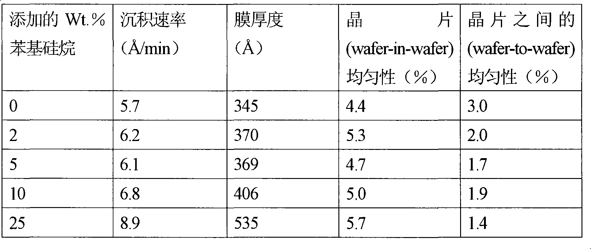
表10Table 10

[0061]至于碳掺杂的氧化硅,我们观察到通过这个方法引入碳能在宽范围的条件下控制。随着苯基硅烷量从0%到25%的增加,我们观察到氮化硅膜密度减小了15%。同时,膜的HF湿法蚀刻速率有显著的减小。典型地,更低的湿法蚀刻速率被归因于更致密的氮化硅膜。[0061] As for carbon-doped silicon oxide, we observed that carbon incorporation by this method can be controlled over a wide range of conditions. We observed a 15% decrease in silicon nitride film density as the amount of phenylsilane was increased from 0% to 25%. At the same time, the HF wet etch rate of the film was significantly reduced. Typically, lower wet etch rates are attributed to denser silicon nitride films.
[0062]图5显示了采用75%BTBAS和25%苯基硅烷的掺混物沉积的氮化硅膜的FT-IR光谱。该图显示了在870cm-1处有强Si-O伸缩吸收峰(stretchabsorbance),并在1100cm-1处带有Si-C带的肩峰,这确认了膜是带有一些结合的碳的氮化硅膜。[0062] Figure 5 shows the FT-IR spectrum of a silicon nitride film deposited using a blend of 75% BTBAS and 25% phenylsilane. The figure shows a strong Si-O stretch absorbance at 870 cm -1 with a shoulder of the Si-C band at 1100 cm -1 , which confirms that the film is nitrogen with some bound carbon Silicon film.
实施例9:从BTBAS和苯基硅烷沉积氮化硅∶较高的前体混合物与氨(NHExample 9: Deposition of Silicon Nitride from BTBAS and Phenylsilane: Higher Precursor Mixture with Ammonia (NH 33 )流)flow 量之比Quantity ratio
[0063]由BTBAS和苯基硅烷的掺混物沉积出氮化硅膜。BTBAS和苯基硅烷的前体混合物流动为14cm,NH3流动为20sccm。前体混合物和氨的流动比率从实施例8中的0.225增加到本实施例中的0.7。本实施例的其他工艺条件与实施例8中相同。另外,与前一个实施例中显示的数值相比,增加了10%到25%之间的两个另外的苯基硅烷掺杂浓度。[0063] A silicon nitride film was deposited from a blend of BTBAS and phenylsilane. The precursor mixture flow of BTBAS and phenylsilane was 14 cm and the NH flow was 20 sccm. The flow ratio of precursor mixture and ammonia was increased from 0.225 in Example 8 to 0.7 in this example. The other processing conditions of this embodiment are the same as in Embodiment 8. In addition, two additional phenylsilane doping concentrations between 10% and 25% were added compared to the values shown in the previous example.
[0064]表11总结了工艺数据,表12总结了组成和膜性能数据。[0064] Table 11 summarizes the process data and Table 12 summarizes the composition and membrane performance data.
表11Table 11

表12Table 12

[0065]较高的前体混合物与氨的流量比率几乎导致膜沉积速率加倍。所述较高前体流动条件的折射率低于那些较低前体流动条件下观察到的折射率。这会预示着结合采用化学和工艺控制变量来降低碳掺杂的氮化硅膜的介电常数是可能的。[0065] Higher flow ratios of precursor mixture to ammonia nearly doubled the film deposition rate. The refractive indices for the higher precursor flow conditions are lower than those observed for the lower precursor flow conditions. This would suggest that it may be possible to reduce the dielectric constant of carbon-doped silicon nitride films using a combination of chemical and process control variables.
[0066]图6显示了1%HF湿法蚀刻速率和密度作为前体混合比率的函数。表9-12中的数据都描绘在了图里。当混合比率增加时,也就是说,混合物中含有相对较多的苯基硅烷时,1%HF湿法蚀刻速率和密度减小。[0066] FIG. 6 shows 1% HF wet etch rate and density as a function of precursor mixing ratio. The data in Tables 9-12 are depicted in the figure. When the mixing ratio increases, that is, when the mixture contains relatively more phenylsilane, the 1% HF wet etching rate and density decrease.
[0067]图7显示了1%HF湿法蚀刻速率和密度作为膜中检测到的碳原子分数的函数。数据来自表9-12。当更多的碳原子分数被结合入氮化硅膜结构中时,1%HF湿法蚀刻速率和密度减小。[0067] Figure 7 shows 1% HF wet etch rate and density as a function of the fraction of carbon atoms detected in the film. Data are from Tables 9-12. The 1% HF wet etch rate and density decrease as more carbon atomic fractions are incorporated into the silicon nitride film structure.
[0068]实施例6-9显示了通过添加2%-75%之间的苯基硅烷到基础BTBAS沉积工艺中,我们能增加沉积速率,减小膜密度,并减小膜的湿法蚀刻速率。据信,较低密度和较低湿法蚀刻速率的令人惊讶的发现,应归于沉积的膜中存在的原子重量为1%-35%之间的碳。因此,那些掺杂碳的氧化硅和掺杂碳的氮化硅膜能被用作湿法蚀刻工艺的蚀刻阻隔层(etch stop barrier)。[0068] Examples 6-9 show that by adding between 2% and 75% of phenylsilane to the base BTBAS deposition process, we can increase the deposition rate, reduce the film density, and reduce the wet etch rate of the film . It is believed that the surprising finding of lower density and lower wet etch rate is due to the presence of between 1% and 35% by atomic weight of carbon in the deposited film. Therefore, those carbon-doped silicon oxide and carbon-doped silicon nitride films can be used as etch stop barriers for wet etching processes.
[0069]前述的实施例和实施方案的描述应该仅被作为举例说明,而不是限制如权利要求所限定的本发明。正如人们能容易了解的,在没有偏离如权利要求中所阐述的本发明的情况下,可采用对前面阐述的特征的众多变化和结合。这些变化并不被认作偏离了本发明的精神和范围,并且所有这些变化都将包括在下列权利要求的范围内。[0069] The foregoing descriptions of examples and embodiments should be considered by way of illustration only, and not as limitations of the invention as defined by the claims. As one can readily appreciate, numerous variations and combinations of the features set forth above can be employed without departing from the invention as set forth in the claims. Such changes are not to be regarded as a departure from the spirit and scope of the invention, and all such changes are intended to be included within the scope of the following claims.
Claims (24)
Applications Claiming Priority (4)
| Application Number | Priority Date | Filing Date | Title |
|---|---|---|---|
| US86132706P | 2006-11-28 | 2006-11-28 | |
| US60/861327 | 2006-11-28 | ||
| US11/941,532 US20080124946A1 (en) | 2006-11-28 | 2007-11-16 | Organosilane compounds for modifying dielectrical properties of silicon oxide and silicon nitride films |
| US11/941532 | 2007-11-16 |
Publications (2)
| Publication Number | Publication Date |
|---|---|
| CN101275219A true CN101275219A (en) | 2008-10-01 |
| CN101275219B CN101275219B (en) | 2013-10-30 |
Family
ID=38969794
Family Applications (1)
| Application Number | Title | Priority Date | Filing Date |
|---|---|---|---|
| CN200710306176XA Expired - Fee Related CN101275219B (en) | 2006-11-28 | 2007-11-28 | Organosilane compounds for modifying dielectrical properties of silicon oxide and silicon nitride films |
Country Status (6)
| Country | Link |
|---|---|
| US (1) | US20080124946A1 (en) |
| EP (1) | EP1928015A3 (en) |
| JP (1) | JP4950011B2 (en) |
| KR (2) | KR101278483B1 (en) |
| CN (1) | CN101275219B (en) |
| TW (1) | TWI363104B (en) |
Cited By (6)
| Publication number | Priority date | Publication date | Assignee | Title |
|---|---|---|---|---|
| CN102423645A (en) * | 2011-10-19 | 2012-04-25 | 南京工业大学 | A method for surface modification of polytetrafluoroethylene separation membrane |
| CN103311119A (en) * | 2012-03-16 | 2013-09-18 | 气体产品与化学公司 | Catalyst synthesis for organosilane sol-gel reactions |
| CN104064446A (en) * | 2013-03-21 | 2014-09-24 | 东京毅力科创株式会社 | Stacked Semiconductor Element, And Method And Apparatus Of Manufacturing The Same |
| CN110021517A (en) * | 2017-11-28 | 2019-07-16 | 台湾积体电路制造股份有限公司 | Semiconductor structure and forming method thereof |
| CN113366141A (en) * | 2018-12-21 | 2021-09-07 | 旭硝子欧洲玻璃公司 | Method for metal coating |
| CN113802108A (en) * | 2020-06-11 | 2021-12-17 | Spts科技有限公司 | Method of deposition |
Families Citing this family (418)
| Publication number | Priority date | Publication date | Assignee | Title |
|---|---|---|---|---|
| US8772524B2 (en) * | 2008-10-20 | 2014-07-08 | Dow Corning Corporation | CVD precursors |
| JP5665289B2 (en) | 2008-10-29 | 2015-02-04 | 株式会社日立国際電気 | Semiconductor device manufacturing method, substrate processing method, and substrate processing apparatus |
| US10378106B2 (en) | 2008-11-14 | 2019-08-13 | Asm Ip Holding B.V. | Method of forming insulation film by modified PEALD |
| US8012887B2 (en) * | 2008-12-18 | 2011-09-06 | Applied Materials, Inc. | Precursor addition to silicon oxide CVD for improved low temperature gapfill |
| US9394608B2 (en) | 2009-04-06 | 2016-07-19 | Asm America, Inc. | Semiconductor processing reactor and components thereof |
| US8802201B2 (en) | 2009-08-14 | 2014-08-12 | Asm America, Inc. | Systems and methods for thin-film deposition of metal oxides using excited nitrogen-oxygen species |
| US8912353B2 (en) | 2010-06-02 | 2014-12-16 | Air Products And Chemicals, Inc. | Organoaminosilane precursors and methods for depositing films comprising same |
| US9447287B2 (en) | 2011-06-03 | 2016-09-20 | Air Products And Chemicals, Inc. | Compositions and processes for depositing carbon-doped silicon-containing films |
| US9312155B2 (en) | 2011-06-06 | 2016-04-12 | Asm Japan K.K. | High-throughput semiconductor-processing apparatus equipped with multiple dual-chamber modules |
| US9793148B2 (en) | 2011-06-22 | 2017-10-17 | Asm Japan K.K. | Method for positioning wafers in multiple wafer transport |
| US10364496B2 (en) | 2011-06-27 | 2019-07-30 | Asm Ip Holding B.V. | Dual section module having shared and unshared mass flow controllers |
| US10854498B2 (en) | 2011-07-15 | 2020-12-01 | Asm Ip Holding B.V. | Wafer-supporting device and method for producing same |
| US20130023129A1 (en) | 2011-07-20 | 2013-01-24 | Asm America, Inc. | Pressure transmitter for a semiconductor processing environment |
| US9017481B1 (en) | 2011-10-28 | 2015-04-28 | Asm America, Inc. | Process feed management for semiconductor substrate processing |
| US9809711B2 (en) | 2012-01-17 | 2017-11-07 | Versum Materials Us, Llc | Catalyst and formulations comprising same for alkoxysilanes hydrolysis reaction in semiconductor process |
| US8592328B2 (en) | 2012-01-20 | 2013-11-26 | Novellus Systems, Inc. | Method for depositing a chlorine-free conformal sin film |
| US20130224964A1 (en) * | 2012-02-28 | 2013-08-29 | Asm Ip Holding B.V. | Method for Forming Dielectric Film Containing Si-C bonds by Atomic Layer Deposition Using Precursor Containing Si-C-Si bond |
| US9460912B2 (en) | 2012-04-12 | 2016-10-04 | Air Products And Chemicals, Inc. | High temperature atomic layer deposition of silicon oxide thin films |
| US9659799B2 (en) | 2012-08-28 | 2017-05-23 | Asm Ip Holding B.V. | Systems and methods for dynamic semiconductor process scheduling |
| US9021985B2 (en) | 2012-09-12 | 2015-05-05 | Asm Ip Holdings B.V. | Process gas management for an inductively-coupled plasma deposition reactor |
| US10714315B2 (en) | 2012-10-12 | 2020-07-14 | Asm Ip Holdings B.V. | Semiconductor reaction chamber showerhead |
| US9640416B2 (en) | 2012-12-26 | 2017-05-02 | Asm Ip Holding B.V. | Single-and dual-chamber module-attachable wafer-handling chamber |
| US20160376700A1 (en) | 2013-02-01 | 2016-12-29 | Asm Ip Holding B.V. | System for treatment of deposition reactor |
| US9589770B2 (en) | 2013-03-08 | 2017-03-07 | Asm Ip Holding B.V. | Method and systems for in-situ formation of intermediate reactive species |
| US9484191B2 (en) | 2013-03-08 | 2016-11-01 | Asm Ip Holding B.V. | Pulsed remote plasma method and system |
| US9793115B2 (en) | 2013-08-14 | 2017-10-17 | Asm Ip Holding B.V. | Structures and devices including germanium-tin films and methods of forming same |
| US9240412B2 (en) | 2013-09-27 | 2016-01-19 | Asm Ip Holding B.V. | Semiconductor structure and device and methods of forming same using selective epitaxial process |
| WO2015046092A1 (en) * | 2013-09-27 | 2015-04-02 | 住友化学株式会社 | Laminated film, organic electroluminescence device, photoelectric conversion device, and liquid crystal display |
| US9556516B2 (en) | 2013-10-09 | 2017-01-31 | ASM IP Holding B.V | Method for forming Ti-containing film by PEALD using TDMAT or TDEAT |
| US10179947B2 (en) | 2013-11-26 | 2019-01-15 | Asm Ip Holding B.V. | Method for forming conformal nitrided, oxidized, or carbonized dielectric film by atomic layer deposition |
| US10683571B2 (en) | 2014-02-25 | 2020-06-16 | Asm Ip Holding B.V. | Gas supply manifold and method of supplying gases to chamber using same |
| US9447498B2 (en) | 2014-03-18 | 2016-09-20 | Asm Ip Holding B.V. | Method for performing uniform processing in gas system-sharing multiple reaction chambers |
| US10167557B2 (en) | 2014-03-18 | 2019-01-01 | Asm Ip Holding B.V. | Gas distribution system, reactor including the system, and methods of using the same |
| US11015245B2 (en) | 2014-03-19 | 2021-05-25 | Asm Ip Holding B.V. | Gas-phase reactor and system having exhaust plenum and components thereof |
| US10858737B2 (en) | 2014-07-28 | 2020-12-08 | Asm Ip Holding B.V. | Showerhead assembly and components thereof |
| US9543180B2 (en) | 2014-08-01 | 2017-01-10 | Asm Ip Holding B.V. | Apparatus and method for transporting wafers between wafer carrier and process tool under vacuum |
| US9890456B2 (en) | 2014-08-21 | 2018-02-13 | Asm Ip Holding B.V. | Method and system for in situ formation of gas-phase compounds |
| US9214333B1 (en) | 2014-09-24 | 2015-12-15 | Lam Research Corporation | Methods and apparatuses for uniform reduction of the in-feature wet etch rate of a silicon nitride film formed by ALD |
| US10941490B2 (en) | 2014-10-07 | 2021-03-09 | Asm Ip Holding B.V. | Multiple temperature range susceptor, assembly, reactor and system including the susceptor, and methods of using the same |
| US9657845B2 (en) | 2014-10-07 | 2017-05-23 | Asm Ip Holding B.V. | Variable conductance gas distribution apparatus and method |
| KR102300403B1 (en) | 2014-11-19 | 2021-09-09 | 에이에스엠 아이피 홀딩 비.브이. | Method of depositing thin film |
| US9589790B2 (en) | 2014-11-24 | 2017-03-07 | Lam Research Corporation | Method of depositing ammonia free and chlorine free conformal silicon nitride film |
| US9564312B2 (en) | 2014-11-24 | 2017-02-07 | Lam Research Corporation | Selective inhibition in atomic layer deposition of silicon-containing films |
| KR102263121B1 (en) | 2014-12-22 | 2021-06-09 | 에이에스엠 아이피 홀딩 비.브이. | Semiconductor device and manufacuring method thereof |
| US10354860B2 (en) | 2015-01-29 | 2019-07-16 | Versum Materials Us, Llc | Method and precursors for manufacturing 3D devices |
| US9478415B2 (en) | 2015-02-13 | 2016-10-25 | Asm Ip Holding B.V. | Method for forming film having low resistance and shallow junction depth |
| US10529542B2 (en) | 2015-03-11 | 2020-01-07 | Asm Ip Holdings B.V. | Cross-flow reactor and method |
| US10276355B2 (en) | 2015-03-12 | 2019-04-30 | Asm Ip Holding B.V. | Multi-zone reactor, system including the reactor, and method of using the same |
| US9502238B2 (en) | 2015-04-03 | 2016-11-22 | Lam Research Corporation | Deposition of conformal films by atomic layer deposition and atomic layer etch |
| US10458018B2 (en) | 2015-06-26 | 2019-10-29 | Asm Ip Holding B.V. | Structures including metal carbide material, devices including the structures, and methods of forming same |
| US10600673B2 (en) | 2015-07-07 | 2020-03-24 | Asm Ip Holding B.V. | Magnetic susceptor to baseplate seal |
| US10043661B2 (en) | 2015-07-13 | 2018-08-07 | Asm Ip Holding B.V. | Method for protecting layer by forming hydrocarbon-based extremely thin film |
| US9899291B2 (en) | 2015-07-13 | 2018-02-20 | Asm Ip Holding B.V. | Method for protecting layer by forming hydrocarbon-based extremely thin film |
| US10083836B2 (en) | 2015-07-24 | 2018-09-25 | Asm Ip Holding B.V. | Formation of boron-doped titanium metal films with high work function |
| US10087525B2 (en) | 2015-08-04 | 2018-10-02 | Asm Ip Holding B.V. | Variable gap hard stop design |
| US9647114B2 (en) | 2015-08-14 | 2017-05-09 | Asm Ip Holding B.V. | Methods of forming highly p-type doped germanium tin films and structures and devices including the films |
| US9711345B2 (en) | 2015-08-25 | 2017-07-18 | Asm Ip Holding B.V. | Method for forming aluminum nitride-based film by PEALD |
| US9601693B1 (en) | 2015-09-24 | 2017-03-21 | Lam Research Corporation | Method for encapsulating a chalcogenide material |
| US9960072B2 (en) | 2015-09-29 | 2018-05-01 | Asm Ip Holding B.V. | Variable adjustment for precise matching of multiple chamber cavity housings |
| US9909214B2 (en) | 2015-10-15 | 2018-03-06 | Asm Ip Holding B.V. | Method for depositing dielectric film in trenches by PEALD |
| US10211308B2 (en) | 2015-10-21 | 2019-02-19 | Asm Ip Holding B.V. | NbMC layers |
| US10322384B2 (en) | 2015-11-09 | 2019-06-18 | Asm Ip Holding B.V. | Counter flow mixer for process chamber |
| US9455138B1 (en) | 2015-11-10 | 2016-09-27 | Asm Ip Holding B.V. | Method for forming dielectric film in trenches by PEALD using H-containing gas |
| US9905420B2 (en) | 2015-12-01 | 2018-02-27 | Asm Ip Holding B.V. | Methods of forming silicon germanium tin films and structures and devices including the films |
| US9607837B1 (en) | 2015-12-21 | 2017-03-28 | Asm Ip Holding B.V. | Method for forming silicon oxide cap layer for solid state diffusion process |
| US9627221B1 (en) | 2015-12-28 | 2017-04-18 | Asm Ip Holding B.V. | Continuous process incorporating atomic layer etching |
| US9735024B2 (en) | 2015-12-28 | 2017-08-15 | Asm Ip Holding B.V. | Method of atomic layer etching using functional group-containing fluorocarbon |
| US11139308B2 (en) | 2015-12-29 | 2021-10-05 | Asm Ip Holding B.V. | Atomic layer deposition of III-V compounds to form V-NAND devices |
| US9754779B1 (en) | 2016-02-19 | 2017-09-05 | Asm Ip Holding B.V. | Method for forming silicon nitride film selectively on sidewalls or flat surfaces of trenches |
| US10529554B2 (en) | 2016-02-19 | 2020-01-07 | Asm Ip Holding B.V. | Method for forming silicon nitride film selectively on sidewalls or flat surfaces of trenches |
| US10468251B2 (en) | 2016-02-19 | 2019-11-05 | Asm Ip Holding B.V. | Method for forming spacers using silicon nitride film for spacer-defined multiple patterning |
| IL261283B2 (en) * | 2016-02-26 | 2025-02-01 | Versum Mat Us Llc | Compositions and methods using same for deposition of silicon-containing film |
| US10501866B2 (en) | 2016-03-09 | 2019-12-10 | Asm Ip Holding B.V. | Gas distribution apparatus for improved film uniformity in an epitaxial system |
| US10343920B2 (en) | 2016-03-18 | 2019-07-09 | Asm Ip Holding B.V. | Aligned carbon nanotubes |
| US9892913B2 (en) | 2016-03-24 | 2018-02-13 | Asm Ip Holding B.V. | Radial and thickness control via biased multi-port injection settings |
| US10190213B2 (en) | 2016-04-21 | 2019-01-29 | Asm Ip Holding B.V. | Deposition of metal borides |
| US10087522B2 (en) | 2016-04-21 | 2018-10-02 | Asm Ip Holding B.V. | Deposition of metal borides |
| US10865475B2 (en) | 2016-04-21 | 2020-12-15 | Asm Ip Holding B.V. | Deposition of metal borides and silicides |
| US10032628B2 (en) | 2016-05-02 | 2018-07-24 | Asm Ip Holding B.V. | Source/drain performance through conformal solid state doping |
| US10367080B2 (en) | 2016-05-02 | 2019-07-30 | Asm Ip Holding B.V. | Method of forming a germanium oxynitride film |
| KR102592471B1 (en) | 2016-05-17 | 2023-10-20 | 에이에스엠 아이피 홀딩 비.브이. | Method of forming metal interconnection and method of fabricating semiconductor device using the same |
| US11453943B2 (en) | 2016-05-25 | 2022-09-27 | Asm Ip Holding B.V. | Method for forming carbon-containing silicon/metal oxide or nitride film by ALD using silicon precursor and hydrocarbon precursor |
| US10388509B2 (en) | 2016-06-28 | 2019-08-20 | Asm Ip Holding B.V. | Formation of epitaxial layers via dislocation filtering |
| US9859151B1 (en) | 2016-07-08 | 2018-01-02 | Asm Ip Holding B.V. | Selective film deposition method to form air gaps |
| US10612137B2 (en) | 2016-07-08 | 2020-04-07 | Asm Ip Holdings B.V. | Organic reactants for atomic layer deposition |
| US9793135B1 (en) | 2016-07-14 | 2017-10-17 | ASM IP Holding B.V | Method of cyclic dry etching using etchant film |
| US10714385B2 (en) | 2016-07-19 | 2020-07-14 | Asm Ip Holding B.V. | Selective deposition of tungsten |
| KR102354490B1 (en) | 2016-07-27 | 2022-01-21 | 에이에스엠 아이피 홀딩 비.브이. | Method of processing a substrate |
| US9812320B1 (en) | 2016-07-28 | 2017-11-07 | Asm Ip Holding B.V. | Method and apparatus for filling a gap |
| US10177025B2 (en) | 2016-07-28 | 2019-01-08 | Asm Ip Holding B.V. | Method and apparatus for filling a gap |
| US10395919B2 (en) | 2016-07-28 | 2019-08-27 | Asm Ip Holding B.V. | Method and apparatus for filling a gap |
| US9887082B1 (en) | 2016-07-28 | 2018-02-06 | Asm Ip Holding B.V. | Method and apparatus for filling a gap |
| KR102532607B1 (en) | 2016-07-28 | 2023-05-15 | 에이에스엠 아이피 홀딩 비.브이. | Substrate processing apparatus and method of operating the same |
| US10629435B2 (en) | 2016-07-29 | 2020-04-21 | Lam Research Corporation | Doped ALD films for semiconductor patterning applications |
| US10074543B2 (en) | 2016-08-31 | 2018-09-11 | Lam Research Corporation | High dry etch rate materials for semiconductor patterning applications |
| US10090316B2 (en) | 2016-09-01 | 2018-10-02 | Asm Ip Holding B.V. | 3D stacked multilayer semiconductor memory using doped select transistor channel |
| US9865455B1 (en) | 2016-09-07 | 2018-01-09 | Lam Research Corporation | Nitride film formed by plasma-enhanced and thermal atomic layer deposition process |
| US10410943B2 (en) | 2016-10-13 | 2019-09-10 | Asm Ip Holding B.V. | Method for passivating a surface of a semiconductor and related systems |
| US10643826B2 (en) | 2016-10-26 | 2020-05-05 | Asm Ip Holdings B.V. | Methods for thermally calibrating reaction chambers |
| US11532757B2 (en) | 2016-10-27 | 2022-12-20 | Asm Ip Holding B.V. | Deposition of charge trapping layers |
| US10714350B2 (en) | 2016-11-01 | 2020-07-14 | ASM IP Holdings, B.V. | Methods for forming a transition metal niobium nitride film on a substrate by atomic layer deposition and related semiconductor device structures |
| US10229833B2 (en) | 2016-11-01 | 2019-03-12 | Asm Ip Holding B.V. | Methods for forming a transition metal nitride film on a substrate by atomic layer deposition and related semiconductor device structures |
| US10643904B2 (en) | 2016-11-01 | 2020-05-05 | Asm Ip Holdings B.V. | Methods for forming a semiconductor device and related semiconductor device structures |
| US10435790B2 (en) | 2016-11-01 | 2019-10-08 | Asm Ip Holding B.V. | Method of subatmospheric plasma-enhanced ALD using capacitively coupled electrodes with narrow gap |
| US10134757B2 (en) | 2016-11-07 | 2018-11-20 | Asm Ip Holding B.V. | Method of processing a substrate and a device manufactured by using the method |
| US10832908B2 (en) | 2016-11-11 | 2020-11-10 | Lam Research Corporation | Self-aligned multi-patterning process flow with ALD gapfill spacer mask |
| US10454029B2 (en) | 2016-11-11 | 2019-10-22 | Lam Research Corporation | Method for reducing the wet etch rate of a sin film without damaging the underlying substrate |
| US10134579B2 (en) | 2016-11-14 | 2018-11-20 | Lam Research Corporation | Method for high modulus ALD SiO2 spacer |
| KR102546317B1 (en) | 2016-11-15 | 2023-06-21 | 에이에스엠 아이피 홀딩 비.브이. | Gas supply unit and substrate processing apparatus including the same |
| US10340135B2 (en) | 2016-11-28 | 2019-07-02 | Asm Ip Holding B.V. | Method of topologically restricted plasma-enhanced cyclic deposition of silicon or metal nitride |
| KR102762543B1 (en) | 2016-12-14 | 2025-02-05 | 에이에스엠 아이피 홀딩 비.브이. | Substrate processing apparatus |
| US11581186B2 (en) | 2016-12-15 | 2023-02-14 | Asm Ip Holding B.V. | Sequential infiltration synthesis apparatus |
| US9916980B1 (en) | 2016-12-15 | 2018-03-13 | Asm Ip Holding B.V. | Method of forming a structure on a substrate |
| US11447861B2 (en) | 2016-12-15 | 2022-09-20 | Asm Ip Holding B.V. | Sequential infiltration synthesis apparatus and a method of forming a patterned structure |
| KR102700194B1 (en) | 2016-12-19 | 2024-08-28 | 에이에스엠 아이피 홀딩 비.브이. | Substrate processing apparatus |
| US10269558B2 (en) | 2016-12-22 | 2019-04-23 | Asm Ip Holding B.V. | Method of forming a structure on a substrate |
| US10867788B2 (en) | 2016-12-28 | 2020-12-15 | Asm Ip Holding B.V. | Method of forming a structure on a substrate |
| US11390950B2 (en) | 2017-01-10 | 2022-07-19 | Asm Ip Holding B.V. | Reactor system and method to reduce residue buildup during a film deposition process |
| US10655221B2 (en) | 2017-02-09 | 2020-05-19 | Asm Ip Holding B.V. | Method for depositing oxide film by thermal ALD and PEALD |
| US10468261B2 (en) | 2017-02-15 | 2019-11-05 | Asm Ip Holding B.V. | Methods for forming a metallic film on a substrate by cyclical deposition and related semiconductor device structures |
| US10529563B2 (en) | 2017-03-29 | 2020-01-07 | Asm Ip Holdings B.V. | Method for forming doped metal oxide films on a substrate by cyclical deposition and related semiconductor device structures |
| US10283353B2 (en) | 2017-03-29 | 2019-05-07 | Asm Ip Holding B.V. | Method of reforming insulating film deposited on substrate with recess pattern |
| US10103040B1 (en) | 2017-03-31 | 2018-10-16 | Asm Ip Holding B.V. | Apparatus and method for manufacturing a semiconductor device |
| USD830981S1 (en) | 2017-04-07 | 2018-10-16 | Asm Ip Holding B.V. | Susceptor for semiconductor substrate processing apparatus |
| KR102457289B1 (en) | 2017-04-25 | 2022-10-21 | 에이에스엠 아이피 홀딩 비.브이. | Method for depositing a thin film and manufacturing a semiconductor device |
| US10446393B2 (en) | 2017-05-08 | 2019-10-15 | Asm Ip Holding B.V. | Methods for forming silicon-containing epitaxial layers and related semiconductor device structures |
| US10892156B2 (en) | 2017-05-08 | 2021-01-12 | Asm Ip Holding B.V. | Methods for forming a silicon nitride film on a substrate and related semiconductor device structures |
| US10770286B2 (en) | 2017-05-08 | 2020-09-08 | Asm Ip Holdings B.V. | Methods for selectively forming a silicon nitride film on a substrate and related semiconductor device structures |
| US10504742B2 (en) | 2017-05-31 | 2019-12-10 | Asm Ip Holding B.V. | Method of atomic layer etching using hydrogen plasma |
| US10886123B2 (en) | 2017-06-02 | 2021-01-05 | Asm Ip Holding B.V. | Methods for forming low temperature semiconductor layers and related semiconductor device structures |
| US12040200B2 (en) | 2017-06-20 | 2024-07-16 | Asm Ip Holding B.V. | Semiconductor processing apparatus and methods for calibrating a semiconductor processing apparatus |
| US11306395B2 (en) | 2017-06-28 | 2022-04-19 | Asm Ip Holding B.V. | Methods for depositing a transition metal nitride film on a substrate by atomic layer deposition and related deposition apparatus |
| US10685834B2 (en) | 2017-07-05 | 2020-06-16 | Asm Ip Holdings B.V. | Methods for forming a silicon germanium tin layer and related semiconductor device structures |
| KR20190009245A (en) | 2017-07-18 | 2019-01-28 | 에이에스엠 아이피 홀딩 비.브이. | Methods for forming a semiconductor device structure and related semiconductor device structures |
| US11018002B2 (en) | 2017-07-19 | 2021-05-25 | Asm Ip Holding B.V. | Method for selectively depositing a Group IV semiconductor and related semiconductor device structures |
| US10541333B2 (en) | 2017-07-19 | 2020-01-21 | Asm Ip Holding B.V. | Method for depositing a group IV semiconductor and related semiconductor device structures |
| US11374112B2 (en) | 2017-07-19 | 2022-06-28 | Asm Ip Holding B.V. | Method for depositing a group IV semiconductor and related semiconductor device structures |
| US10605530B2 (en) | 2017-07-26 | 2020-03-31 | Asm Ip Holding B.V. | Assembly of a liner and a flange for a vertical furnace as well as the liner and the vertical furnace |
| US10312055B2 (en) | 2017-07-26 | 2019-06-04 | Asm Ip Holding B.V. | Method of depositing film by PEALD using negative bias |
| US10590535B2 (en) | 2017-07-26 | 2020-03-17 | Asm Ip Holdings B.V. | Chemical treatment, deposition and/or infiltration apparatus and method for using the same |
| TWI815813B (en) | 2017-08-04 | 2023-09-21 | 荷蘭商Asm智慧財產控股公司 | Showerhead assembly for distributing a gas within a reaction chamber |
| US10770336B2 (en) | 2017-08-08 | 2020-09-08 | Asm Ip Holding B.V. | Substrate lift mechanism and reactor including same |
| US10692741B2 (en) | 2017-08-08 | 2020-06-23 | Asm Ip Holdings B.V. | Radiation shield |
| US10249524B2 (en) | 2017-08-09 | 2019-04-02 | Asm Ip Holding B.V. | Cassette holder assembly for a substrate cassette and holding member for use in such assembly |
| US11139191B2 (en) | 2017-08-09 | 2021-10-05 | Asm Ip Holding B.V. | Storage apparatus for storing cassettes for substrates and processing apparatus equipped therewith |
| US11769682B2 (en) | 2017-08-09 | 2023-09-26 | Asm Ip Holding B.V. | Storage apparatus for storing cassettes for substrates and processing apparatus equipped therewith |
| US10236177B1 (en) | 2017-08-22 | 2019-03-19 | ASM IP Holding B.V.. | Methods for depositing a doped germanium tin semiconductor and related semiconductor device structures |
| USD900036S1 (en) | 2017-08-24 | 2020-10-27 | Asm Ip Holding B.V. | Heater electrical connector and adapter |
| US11282845B2 (en) * | 2017-08-24 | 2022-03-22 | Micron Technology, Inc. | Semiconductor devices comprising carbon-doped silicon nitride and related methods |
| US11830730B2 (en) | 2017-08-29 | 2023-11-28 | Asm Ip Holding B.V. | Layer forming method and apparatus |
| KR102491945B1 (en) | 2017-08-30 | 2023-01-26 | 에이에스엠 아이피 홀딩 비.브이. | Substrate processing apparatus |
| US11056344B2 (en) | 2017-08-30 | 2021-07-06 | Asm Ip Holding B.V. | Layer forming method |
| US11295980B2 (en) | 2017-08-30 | 2022-04-05 | Asm Ip Holding B.V. | Methods for depositing a molybdenum metal film over a dielectric surface of a substrate by a cyclical deposition process and related semiconductor device structures |
| KR102401446B1 (en) | 2017-08-31 | 2022-05-24 | 에이에스엠 아이피 홀딩 비.브이. | Substrate processing apparatus |
| US10269559B2 (en) | 2017-09-13 | 2019-04-23 | Lam Research Corporation | Dielectric gapfill of high aspect ratio features utilizing a sacrificial etch cap layer |
| US10607895B2 (en) | 2017-09-18 | 2020-03-31 | Asm Ip Holdings B.V. | Method for forming a semiconductor device structure comprising a gate fill metal |
| KR102630301B1 (en) | 2017-09-21 | 2024-01-29 | 에이에스엠 아이피 홀딩 비.브이. | Method of sequential infiltration synthesis treatment of infiltrateable material and structures and devices formed using same |
| US10844484B2 (en) | 2017-09-22 | 2020-11-24 | Asm Ip Holding B.V. | Apparatus for dispensing a vapor phase reactant to a reaction chamber and related methods |
| US10658205B2 (en) | 2017-09-28 | 2020-05-19 | Asm Ip Holdings B.V. | Chemical dispensing apparatus and methods for dispensing a chemical to a reaction chamber |
| US10403504B2 (en) | 2017-10-05 | 2019-09-03 | Asm Ip Holding B.V. | Method for selectively depositing a metallic film on a substrate |
| US10319588B2 (en) | 2017-10-10 | 2019-06-11 | Asm Ip Holding B.V. | Method for depositing a metal chalcogenide on a substrate by cyclical deposition |
| US10923344B2 (en) | 2017-10-30 | 2021-02-16 | Asm Ip Holding B.V. | Methods for forming a semiconductor structure and related semiconductor structures |
| KR102443047B1 (en) | 2017-11-16 | 2022-09-14 | 에이에스엠 아이피 홀딩 비.브이. | Substrate processing apparatus method and apparatus manufactured thereby |
| US10910262B2 (en) | 2017-11-16 | 2021-02-02 | Asm Ip Holding B.V. | Method of selectively depositing a capping layer structure on a semiconductor device structure |
| US11022879B2 (en) | 2017-11-24 | 2021-06-01 | Asm Ip Holding B.V. | Method of forming an enhanced unexposed photoresist layer |
| CN111344522B (en) | 2017-11-27 | 2022-04-12 | 阿斯莫Ip控股公司 | Units including clean mini environments |
| KR102597978B1 (en) | 2017-11-27 | 2023-11-06 | 에이에스엠 아이피 홀딩 비.브이. | Storage device for storing wafer cassettes for use with batch furnaces |
| US10290508B1 (en) | 2017-12-05 | 2019-05-14 | Asm Ip Holding B.V. | Method for forming vertical spacers for spacer-defined patterning |
| US10872771B2 (en) | 2018-01-16 | 2020-12-22 | Asm Ip Holding B. V. | Method for depositing a material film on a substrate within a reaction chamber by a cyclical deposition process and related device structures |
| TWI799494B (en) | 2018-01-19 | 2023-04-21 | 荷蘭商Asm 智慧財產控股公司 | Deposition method |
| WO2019142055A2 (en) | 2018-01-19 | 2019-07-25 | Asm Ip Holding B.V. | Method for depositing a gap-fill layer by plasma-assisted deposition |
| USD903477S1 (en) | 2018-01-24 | 2020-12-01 | Asm Ip Holdings B.V. | Metal clamp |
| US11018047B2 (en) | 2018-01-25 | 2021-05-25 | Asm Ip Holding B.V. | Hybrid lift pin |
| US10535516B2 (en) | 2018-02-01 | 2020-01-14 | Asm Ip Holdings B.V. | Method for depositing a semiconductor structure on a surface of a substrate and related semiconductor structures |
| USD880437S1 (en) | 2018-02-01 | 2020-04-07 | Asm Ip Holding B.V. | Gas supply plate for semiconductor manufacturing apparatus |
| US11081345B2 (en) | 2018-02-06 | 2021-08-03 | Asm Ip Holding B.V. | Method of post-deposition treatment for silicon oxide film |
| US11685991B2 (en) | 2018-02-14 | 2023-06-27 | Asm Ip Holding B.V. | Method for depositing a ruthenium-containing film on a substrate by a cyclical deposition process |
| US10896820B2 (en) | 2018-02-14 | 2021-01-19 | Asm Ip Holding B.V. | Method for depositing a ruthenium-containing film on a substrate by a cyclical deposition process |
| US10731249B2 (en) | 2018-02-15 | 2020-08-04 | Asm Ip Holding B.V. | Method of forming a transition metal containing film on a substrate by a cyclical deposition process, a method for supplying a transition metal halide compound to a reaction chamber, and related vapor deposition apparatus |
| US10658181B2 (en) | 2018-02-20 | 2020-05-19 | Asm Ip Holding B.V. | Method of spacer-defined direct patterning in semiconductor fabrication |
| KR102636427B1 (en) | 2018-02-20 | 2024-02-13 | 에이에스엠 아이피 홀딩 비.브이. | Substrate processing method and apparatus |
| US10975470B2 (en) | 2018-02-23 | 2021-04-13 | Asm Ip Holding B.V. | Apparatus for detecting or monitoring for a chemical precursor in a high temperature environment |
| US11473195B2 (en) | 2018-03-01 | 2022-10-18 | Asm Ip Holding B.V. | Semiconductor processing apparatus and a method for processing a substrate |
| US11404275B2 (en) | 2018-03-02 | 2022-08-02 | Lam Research Corporation | Selective deposition using hydrolysis |
| US11629406B2 (en) | 2018-03-09 | 2023-04-18 | Asm Ip Holding B.V. | Semiconductor processing apparatus comprising one or more pyrometers for measuring a temperature of a substrate during transfer of the substrate |
| US11114283B2 (en) | 2018-03-16 | 2021-09-07 | Asm Ip Holding B.V. | Reactor, system including the reactor, and methods of manufacturing and using same |
| KR102646467B1 (en) | 2018-03-27 | 2024-03-11 | 에이에스엠 아이피 홀딩 비.브이. | Method of forming an electrode on a substrate and a semiconductor device structure including an electrode |
| US11230766B2 (en) | 2018-03-29 | 2022-01-25 | Asm Ip Holding B.V. | Substrate processing apparatus and method |
| US10510536B2 (en) | 2018-03-29 | 2019-12-17 | Asm Ip Holding B.V. | Method of depositing a co-doped polysilicon film on a surface of a substrate within a reaction chamber |
| US11088002B2 (en) | 2018-03-29 | 2021-08-10 | Asm Ip Holding B.V. | Substrate rack and a substrate processing system and method |
| KR102501472B1 (en) | 2018-03-30 | 2023-02-20 | 에이에스엠 아이피 홀딩 비.브이. | Substrate processing method |
| KR102600229B1 (en) | 2018-04-09 | 2023-11-10 | 에이에스엠 아이피 홀딩 비.브이. | Substrate supporting device, substrate processing apparatus including the same and substrate processing method |
| US12025484B2 (en) | 2018-05-08 | 2024-07-02 | Asm Ip Holding B.V. | Thin film forming method |
| TWI811348B (en) | 2018-05-08 | 2023-08-11 | 荷蘭商Asm 智慧財產控股公司 | Methods for depositing an oxide film on a substrate by a cyclical deposition process and related device structures |
| US12272527B2 (en) | 2018-05-09 | 2025-04-08 | Asm Ip Holding B.V. | Apparatus for use with hydrogen radicals and method of using same |
| TWI816783B (en) | 2018-05-11 | 2023-10-01 | 荷蘭商Asm 智慧財產控股公司 | Methods for forming a doped metal carbide film on a substrate and related semiconductor device structures |
| KR102596988B1 (en) | 2018-05-28 | 2023-10-31 | 에이에스엠 아이피 홀딩 비.브이. | Method of processing a substrate and a device manufactured by the same |
| US11718913B2 (en) | 2018-06-04 | 2023-08-08 | Asm Ip Holding B.V. | Gas distribution system and reactor system including same |
| TWI840362B (en) | 2018-06-04 | 2024-05-01 | 荷蘭商Asm Ip私人控股有限公司 | Wafer handling chamber with moisture reduction |
| US11286562B2 (en) | 2018-06-08 | 2022-03-29 | Asm Ip Holding B.V. | Gas-phase chemical reactor and method of using same |
| KR102568797B1 (en) | 2018-06-21 | 2023-08-21 | 에이에스엠 아이피 홀딩 비.브이. | Substrate processing system |
| US10797133B2 (en) | 2018-06-21 | 2020-10-06 | Asm Ip Holding B.V. | Method for depositing a phosphorus doped silicon arsenide film and related semiconductor device structures |
| KR102854019B1 (en) | 2018-06-27 | 2025-09-02 | 에이에스엠 아이피 홀딩 비.브이. | Periodic deposition method for forming a metal-containing material and films and structures comprising the metal-containing material |
| TWI815915B (en) | 2018-06-27 | 2023-09-21 | 荷蘭商Asm Ip私人控股有限公司 | Cyclic deposition methods for forming metal-containing material and films and structures including the metal-containing material |
| KR102686758B1 (en) | 2018-06-29 | 2024-07-18 | 에이에스엠 아이피 홀딩 비.브이. | Method for depositing a thin film and manufacturing a semiconductor device |
| US10612136B2 (en) | 2018-06-29 | 2020-04-07 | ASM IP Holding, B.V. | Temperature-controlled flange and reactor system including same |
| US10388513B1 (en) | 2018-07-03 | 2019-08-20 | Asm Ip Holding B.V. | Method for depositing silicon-free carbon-containing film as gap-fill layer by pulse plasma-assisted deposition |
| US10755922B2 (en) | 2018-07-03 | 2020-08-25 | Asm Ip Holding B.V. | Method for depositing silicon-free carbon-containing film as gap-fill layer by pulse plasma-assisted deposition |
| US10767789B2 (en) | 2018-07-16 | 2020-09-08 | Asm Ip Holding B.V. | Diaphragm valves, valve components, and methods for forming valve components |
| US10483099B1 (en) | 2018-07-26 | 2019-11-19 | Asm Ip Holding B.V. | Method for forming thermally stable organosilicon polymer film |
| US11053591B2 (en) | 2018-08-06 | 2021-07-06 | Asm Ip Holding B.V. | Multi-port gas injection system and reactor system including same |
| US10883175B2 (en) | 2018-08-09 | 2021-01-05 | Asm Ip Holding B.V. | Vertical furnace for processing substrates and a liner for use therein |
| US10829852B2 (en) | 2018-08-16 | 2020-11-10 | Asm Ip Holding B.V. | Gas distribution device for a wafer processing apparatus |
| US11430674B2 (en) | 2018-08-22 | 2022-08-30 | Asm Ip Holding B.V. | Sensor array, apparatus for dispensing a vapor phase reactant to a reaction chamber and related methods |
| KR102707956B1 (en) | 2018-09-11 | 2024-09-19 | 에이에스엠 아이피 홀딩 비.브이. | Method for deposition of a thin film |
| US11024523B2 (en) | 2018-09-11 | 2021-06-01 | Asm Ip Holding B.V. | Substrate processing apparatus and method |
| US11049751B2 (en) | 2018-09-14 | 2021-06-29 | Asm Ip Holding B.V. | Cassette supply system to store and handle cassettes and processing apparatus equipped therewith |
| CN110970344B (en) | 2018-10-01 | 2024-10-25 | Asmip控股有限公司 | Substrate holding device, system including the same and method of using the same |
| US11232963B2 (en) | 2018-10-03 | 2022-01-25 | Asm Ip Holding B.V. | Substrate processing apparatus and method |
| US10971357B2 (en) * | 2018-10-04 | 2021-04-06 | Applied Materials, Inc. | Thin film treatment process |
| KR102592699B1 (en) | 2018-10-08 | 2023-10-23 | 에이에스엠 아이피 홀딩 비.브이. | Substrate support unit and apparatuses for depositing thin film and processing the substrate including the same |
| US10847365B2 (en) | 2018-10-11 | 2020-11-24 | Asm Ip Holding B.V. | Method of forming conformal silicon carbide film by cyclic CVD |
| US10811256B2 (en) | 2018-10-16 | 2020-10-20 | Asm Ip Holding B.V. | Method for etching a carbon-containing feature |
| KR102605121B1 (en) | 2018-10-19 | 2023-11-23 | 에이에스엠 아이피 홀딩 비.브이. | Substrate processing apparatus and substrate processing method |
| KR102546322B1 (en) | 2018-10-19 | 2023-06-21 | 에이에스엠 아이피 홀딩 비.브이. | Substrate processing apparatus and substrate processing method |
| USD948463S1 (en) | 2018-10-24 | 2022-04-12 | Asm Ip Holding B.V. | Susceptor for semiconductor substrate supporting apparatus |
| US10381219B1 (en) | 2018-10-25 | 2019-08-13 | Asm Ip Holding B.V. | Methods for forming a silicon nitride film |
| US12378665B2 (en) | 2018-10-26 | 2025-08-05 | Asm Ip Holding B.V. | High temperature coatings for a preclean and etch apparatus and related methods |
| US11087997B2 (en) | 2018-10-31 | 2021-08-10 | Asm Ip Holding B.V. | Substrate processing apparatus for processing substrates |
| KR102748291B1 (en) | 2018-11-02 | 2024-12-31 | 에이에스엠 아이피 홀딩 비.브이. | Substrate support unit and substrate processing apparatus including the same |
| US11572620B2 (en) | 2018-11-06 | 2023-02-07 | Asm Ip Holding B.V. | Methods for selectively depositing an amorphous silicon film on a substrate |
| US11031242B2 (en) | 2018-11-07 | 2021-06-08 | Asm Ip Holding B.V. | Methods for depositing a boron doped silicon germanium film |
| US10847366B2 (en) | 2018-11-16 | 2020-11-24 | Asm Ip Holding B.V. | Methods for depositing a transition metal chalcogenide film on a substrate by a cyclical deposition process |
| US10818758B2 (en) | 2018-11-16 | 2020-10-27 | Asm Ip Holding B.V. | Methods for forming a metal silicate film on a substrate in a reaction chamber and related semiconductor device structures |
| US10559458B1 (en) | 2018-11-26 | 2020-02-11 | Asm Ip Holding B.V. | Method of forming oxynitride film |
| US12040199B2 (en) | 2018-11-28 | 2024-07-16 | Asm Ip Holding B.V. | Substrate processing apparatus for processing substrates |
| US11217444B2 (en) | 2018-11-30 | 2022-01-04 | Asm Ip Holding B.V. | Method for forming an ultraviolet radiation responsive metal oxide-containing film |
| KR102636428B1 (en) | 2018-12-04 | 2024-02-13 | 에이에스엠 아이피 홀딩 비.브이. | A method for cleaning a substrate processing apparatus |
| US11158513B2 (en) | 2018-12-13 | 2021-10-26 | Asm Ip Holding B.V. | Methods for forming a rhenium-containing film on a substrate by a cyclical deposition process and related semiconductor device structures |
| JP7504584B2 (en) | 2018-12-14 | 2024-06-24 | エーエスエム・アイピー・ホールディング・ベー・フェー | Method and system for forming device structures using selective deposition of gallium nitride - Patents.com |
| TWI819180B (en) | 2019-01-17 | 2023-10-21 | 荷蘭商Asm 智慧財產控股公司 | Methods of forming a transition metal containing film on a substrate by a cyclical deposition process |
| KR102727227B1 (en) | 2019-01-22 | 2024-11-07 | 에이에스엠 아이피 홀딩 비.브이. | Semiconductor processing device |
| CN111524788B (en) | 2019-02-01 | 2023-11-24 | Asm Ip私人控股有限公司 | Method for forming topologically selective films of silicon oxide |
| KR102626263B1 (en) | 2019-02-20 | 2024-01-16 | 에이에스엠 아이피 홀딩 비.브이. | Cyclical deposition method including treatment step and apparatus for same |
| TWI845607B (en) | 2019-02-20 | 2024-06-21 | 荷蘭商Asm Ip私人控股有限公司 | Cyclical deposition method and apparatus for filling a recess formed within a substrate surface |
| US11482533B2 (en) | 2019-02-20 | 2022-10-25 | Asm Ip Holding B.V. | Apparatus and methods for plug fill deposition in 3-D NAND applications |
| JP7603377B2 (en) | 2019-02-20 | 2024-12-20 | エーエスエム・アイピー・ホールディング・ベー・フェー | Method and apparatus for filling recesses formed in a substrate surface - Patents.com |
| TWI842826B (en) | 2019-02-22 | 2024-05-21 | 荷蘭商Asm Ip私人控股有限公司 | Substrate processing apparatus and method for processing substrate |
| KR102762833B1 (en) | 2019-03-08 | 2025-02-04 | 에이에스엠 아이피 홀딩 비.브이. | STRUCTURE INCLUDING SiOCN LAYER AND METHOD OF FORMING SAME |
| KR102782593B1 (en) | 2019-03-08 | 2025-03-14 | 에이에스엠 아이피 홀딩 비.브이. | Structure Including SiOC Layer and Method of Forming Same |
| KR102858005B1 (en) | 2019-03-08 | 2025-09-09 | 에이에스엠 아이피 홀딩 비.브이. | Method for Selective Deposition of Silicon Nitride Layer and Structure Including Selectively-Deposited Silicon Nitride Layer |
| JP2020167398A (en) | 2019-03-28 | 2020-10-08 | エーエスエム・アイピー・ホールディング・ベー・フェー | Door openers and substrate processing equipment provided with door openers |
| KR102809999B1 (en) | 2019-04-01 | 2025-05-19 | 에이에스엠 아이피 홀딩 비.브이. | Method of manufacturing semiconductor device |
| KR102897355B1 (en) | 2019-04-19 | 2025-12-08 | 에이에스엠 아이피 홀딩 비.브이. | Layer forming method and apparatus |
| KR20200125453A (en) | 2019-04-24 | 2020-11-04 | 에이에스엠 아이피 홀딩 비.브이. | Gas-phase reactor system and method of using same |
| KR20200130121A (en) | 2019-05-07 | 2020-11-18 | 에이에스엠 아이피 홀딩 비.브이. | Chemical source vessel with dip tube |
| KR102869364B1 (en) | 2019-05-07 | 2025-10-10 | 에이에스엠 아이피 홀딩 비.브이. | Method for Reforming Amorphous Carbon Polymer Film |
| KR20200130652A (en) | 2019-05-10 | 2020-11-19 | 에이에스엠 아이피 홀딩 비.브이. | Method of depositing material onto a surface and structure formed according to the method |
| JP7612342B2 (en) | 2019-05-16 | 2025-01-14 | エーエスエム・アイピー・ホールディング・ベー・フェー | Wafer boat handling apparatus, vertical batch furnace and method |
| JP7598201B2 (en) | 2019-05-16 | 2024-12-11 | エーエスエム・アイピー・ホールディング・ベー・フェー | Wafer boat handling apparatus, vertical batch furnace and method |
| USD947913S1 (en) | 2019-05-17 | 2022-04-05 | Asm Ip Holding B.V. | Susceptor shaft |
| USD975665S1 (en) | 2019-05-17 | 2023-01-17 | Asm Ip Holding B.V. | Susceptor shaft |
| USD935572S1 (en) | 2019-05-24 | 2021-11-09 | Asm Ip Holding B.V. | Gas channel plate |
| US12237175B2 (en) | 2019-06-04 | 2025-02-25 | Lam Research Corporation | Polymerization protective liner for reactive ion etch in patterning |
| USD922229S1 (en) | 2019-06-05 | 2021-06-15 | Asm Ip Holding B.V. | Device for controlling a temperature of a gas supply unit |
| KR20200141002A (en) | 2019-06-06 | 2020-12-17 | 에이에스엠 아이피 홀딩 비.브이. | Method of using a gas-phase reactor system including analyzing exhausted gas |
| US12252785B2 (en) | 2019-06-10 | 2025-03-18 | Asm Ip Holding B.V. | Method for cleaning quartz epitaxial chambers |
| KR20200143254A (en) | 2019-06-11 | 2020-12-23 | 에이에스엠 아이피 홀딩 비.브이. | Method of forming an electronic structure using an reforming gas, system for performing the method, and structure formed using the method |
| USD944946S1 (en) | 2019-06-14 | 2022-03-01 | Asm Ip Holding B.V. | Shower plate |
| USD931978S1 (en) | 2019-06-27 | 2021-09-28 | Asm Ip Holding B.V. | Showerhead vacuum transport |
| KR102911421B1 (en) | 2019-07-03 | 2026-01-12 | 에이에스엠 아이피 홀딩 비.브이. | Temperature control assembly for substrate processing apparatus and method of using same |
| JP7499079B2 (en) | 2019-07-09 | 2024-06-13 | エーエスエム・アイピー・ホールディング・ベー・フェー | Plasma device using coaxial waveguide and substrate processing method |
| KR20210008310A (en) | 2019-07-10 | 2021-01-21 | 에이에스엠 아이피 홀딩 비.브이. | Substrate supporting assembly and substrate processing apparatus comprising the same |
| KR102895115B1 (en) | 2019-07-16 | 2025-12-03 | 에이에스엠 아이피 홀딩 비.브이. | Substrate processing apparatus |
| KR20210010816A (en) | 2019-07-17 | 2021-01-28 | 에이에스엠 아이피 홀딩 비.브이. | Radical assist ignition plasma system and method |
| KR102860110B1 (en) | 2019-07-17 | 2025-09-16 | 에이에스엠 아이피 홀딩 비.브이. | Methods of forming silicon germanium structures |
| US11643724B2 (en) | 2019-07-18 | 2023-05-09 | Asm Ip Holding B.V. | Method of forming structures using a neutral beam |
| KR102903090B1 (en) | 2019-07-19 | 2025-12-19 | 에이에스엠 아이피 홀딩 비.브이. | Method of Forming Topology-Controlled Amorphous Carbon Polymer Film |
| TWI839544B (en) | 2019-07-19 | 2024-04-21 | 荷蘭商Asm Ip私人控股有限公司 | Method of forming topology-controlled amorphous carbon polymer film |
| TWI851767B (en) | 2019-07-29 | 2024-08-11 | 荷蘭商Asm Ip私人控股有限公司 | Methods for selective deposition utilizing n-type dopants and/or alternative dopants to achieve high dopant incorporation |
| CN112309900B (en) | 2019-07-30 | 2025-11-04 | Asmip私人控股有限公司 | Substrate processing equipment |
| KR20210015655A (en) | 2019-07-30 | 2021-02-10 | 에이에스엠 아이피 홀딩 비.브이. | Substrate processing apparatus and method |
| CN112309899B (en) | 2019-07-30 | 2025-11-14 | Asmip私人控股有限公司 | Substrate processing equipment |
| US11587815B2 (en) | 2019-07-31 | 2023-02-21 | Asm Ip Holding B.V. | Vertical batch furnace assembly |
| US11587814B2 (en) | 2019-07-31 | 2023-02-21 | Asm Ip Holding B.V. | Vertical batch furnace assembly |
| US11227782B2 (en) | 2019-07-31 | 2022-01-18 | Asm Ip Holding B.V. | Vertical batch furnace assembly |
| KR20210018759A (en) | 2019-08-05 | 2021-02-18 | 에이에스엠 아이피 홀딩 비.브이. | Liquid level sensor for a chemical source vessel |
| KR20220042442A (en) | 2019-08-06 | 2022-04-05 | 램 리써치 코포레이션 | Thermal atomic layer deposition of silicon-containing films |
| CN112342526A (en) | 2019-08-09 | 2021-02-09 | Asm Ip私人控股有限公司 | Heater assembly including cooling device and method of using same |
| USD965524S1 (en) | 2019-08-19 | 2022-10-04 | Asm Ip Holding B.V. | Susceptor support |
| USD965044S1 (en) | 2019-08-19 | 2022-09-27 | Asm Ip Holding B.V. | Susceptor shaft |
| US11639548B2 (en) | 2019-08-21 | 2023-05-02 | Asm Ip Holding B.V. | Film-forming material mixed-gas forming device and film forming device |
| USD940837S1 (en) | 2019-08-22 | 2022-01-11 | Asm Ip Holding B.V. | Electrode |
| USD949319S1 (en) | 2019-08-22 | 2022-04-19 | Asm Ip Holding B.V. | Exhaust duct |
| USD979506S1 (en) | 2019-08-22 | 2023-02-28 | Asm Ip Holding B.V. | Insulator |
| KR20210024423A (en) | 2019-08-22 | 2021-03-05 | 에이에스엠 아이피 홀딩 비.브이. | Method for forming a structure with a hole |
| USD930782S1 (en) | 2019-08-22 | 2021-09-14 | Asm Ip Holding B.V. | Gas distributor |
| US11286558B2 (en) | 2019-08-23 | 2022-03-29 | Asm Ip Holding B.V. | Methods for depositing a molybdenum nitride film on a surface of a substrate by a cyclical deposition process and related semiconductor device structures including a molybdenum nitride film |
| TWI838570B (en) | 2019-08-23 | 2024-04-11 | 荷蘭商Asm Ip私人控股有限公司 | Method for depositing silicon oxide film having improved quality by peald using bis(diethylamino)silane |
| KR102868968B1 (en) | 2019-09-03 | 2025-10-10 | 에이에스엠 아이피 홀딩 비.브이. | Methods and apparatus for depositing a chalcogenide film and structures including the film |
| KR102806450B1 (en) | 2019-09-04 | 2025-05-12 | 에이에스엠 아이피 홀딩 비.브이. | Methods for selective deposition using a sacrificial capping layer |
| KR102733104B1 (en) | 2019-09-05 | 2024-11-22 | 에이에스엠 아이피 홀딩 비.브이. | Substrate processing apparatus |
| US12469693B2 (en) | 2019-09-17 | 2025-11-11 | Asm Ip Holding B.V. | Method of forming a carbon-containing layer and structure including the layer |
| US11562901B2 (en) | 2019-09-25 | 2023-01-24 | Asm Ip Holding B.V. | Substrate processing method |
| CN112593212B (en) | 2019-10-02 | 2023-12-22 | Asm Ip私人控股有限公司 | Method for forming topologically selective silicon oxide film through cyclic plasma enhanced deposition process |
| KR20210042810A (en) | 2019-10-08 | 2021-04-20 | 에이에스엠 아이피 홀딩 비.브이. | Reactor system including a gas distribution assembly for use with activated species and method of using same |
| TW202128273A (en) | 2019-10-08 | 2021-08-01 | 荷蘭商Asm Ip私人控股有限公司 | Gas injection system, reactor system, and method of depositing material on surface of substratewithin reaction chamber |
| TWI846953B (en) | 2019-10-08 | 2024-07-01 | 荷蘭商Asm Ip私人控股有限公司 | Substrate processing device |
| TWI846966B (en) | 2019-10-10 | 2024-07-01 | 荷蘭商Asm Ip私人控股有限公司 | Method of forming a photoresist underlayer and structure including same |
| US12009241B2 (en) | 2019-10-14 | 2024-06-11 | Asm Ip Holding B.V. | Vertical batch furnace assembly with detector to detect cassette |
| TWI834919B (en) | 2019-10-16 | 2024-03-11 | 荷蘭商Asm Ip私人控股有限公司 | Method of topology-selective film formation of silicon oxide |
| US11637014B2 (en) | 2019-10-17 | 2023-04-25 | Asm Ip Holding B.V. | Methods for selective deposition of doped semiconductor material |
| KR102845724B1 (en) | 2019-10-21 | 2025-08-13 | 에이에스엠 아이피 홀딩 비.브이. | Apparatus and methods for selectively etching films |
| KR20210050453A (en) | 2019-10-25 | 2021-05-07 | 에이에스엠 아이피 홀딩 비.브이. | Methods for filling a gap feature on a substrate surface and related semiconductor structures |
| US11646205B2 (en) | 2019-10-29 | 2023-05-09 | Asm Ip Holding B.V. | Methods of selectively forming n-type doped material on a surface, systems for selectively forming n-type doped material, and structures formed using same |
| KR102890638B1 (en) | 2019-11-05 | 2025-11-25 | 에이에스엠 아이피 홀딩 비.브이. | Structures with doped semiconductor layers and methods and systems for forming same |
| US11501968B2 (en) | 2019-11-15 | 2022-11-15 | Asm Ip Holding B.V. | Method for providing a semiconductor device with silicon filled gaps |
| KR102861314B1 (en) | 2019-11-20 | 2025-09-17 | 에이에스엠 아이피 홀딩 비.브이. | Method of depositing carbon-containing material on a surface of a substrate, structure formed using the method, and system for forming the structure |
| CN112951697B (en) | 2019-11-26 | 2025-07-29 | Asmip私人控股有限公司 | Substrate processing apparatus |
| KR20210065848A (en) | 2019-11-26 | 2021-06-04 | 에이에스엠 아이피 홀딩 비.브이. | Methods for selectivley forming a target film on a substrate comprising a first dielectric surface and a second metallic surface |
| CN120432376A (en) | 2019-11-29 | 2025-08-05 | Asm Ip私人控股有限公司 | Substrate processing equipment |
| CN112885692B (en) | 2019-11-29 | 2025-08-15 | Asmip私人控股有限公司 | Substrate processing apparatus |
| JP7527928B2 (en) | 2019-12-02 | 2024-08-05 | エーエスエム・アイピー・ホールディング・ベー・フェー | Substrate processing apparatus and substrate processing method |
| KR20210070898A (en) | 2019-12-04 | 2021-06-15 | 에이에스엠 아이피 홀딩 비.브이. | Substrate processing apparatus |
| US11885013B2 (en) | 2019-12-17 | 2024-01-30 | Asm Ip Holding B.V. | Method of forming vanadium nitride layer and structure including the vanadium nitride layer |
| US11527403B2 (en) | 2019-12-19 | 2022-12-13 | Asm Ip Holding B.V. | Methods for filling a gap feature on a substrate surface and related semiconductor structures |
| KR20210089079A (en) | 2020-01-06 | 2021-07-15 | 에이에스엠 아이피 홀딩 비.브이. | Channeled lift pin |
| JP7730637B2 (en) | 2020-01-06 | 2025-08-28 | エーエスエム・アイピー・ホールディング・ベー・フェー | Gas delivery assembly, components thereof, and reactor system including same |
| US11993847B2 (en) | 2020-01-08 | 2024-05-28 | Asm Ip Holding B.V. | Injector |
| KR102882467B1 (en) | 2020-01-16 | 2025-11-05 | 에이에스엠 아이피 홀딩 비.브이. | Method of forming high aspect ratio features |
| KR102675856B1 (en) | 2020-01-20 | 2024-06-17 | 에이에스엠 아이피 홀딩 비.브이. | Method of forming thin film and method of modifying surface of thin film |
| TWI889744B (en) | 2020-01-29 | 2025-07-11 | 荷蘭商Asm Ip私人控股有限公司 | Contaminant trap system, and baffle plate stack |
| TW202513845A (en) | 2020-02-03 | 2025-04-01 | 荷蘭商Asm Ip私人控股有限公司 | Semiconductor structures and methods for forming the same |
| KR20210100010A (en) | 2020-02-04 | 2021-08-13 | 에이에스엠 아이피 홀딩 비.브이. | Method and apparatus for transmittance measurements of large articles |
| US11776846B2 (en) | 2020-02-07 | 2023-10-03 | Asm Ip Holding B.V. | Methods for depositing gap filling fluids and related systems and devices |
| TW202146691A (en) | 2020-02-13 | 2021-12-16 | 荷蘭商Asm Ip私人控股有限公司 | Gas distribution assembly, shower plate assembly, and method of adjusting conductance of gas to reaction chamber |
| CN113257655A (en) | 2020-02-13 | 2021-08-13 | Asm Ip私人控股有限公司 | Substrate processing apparatus including light receiving device and calibration method of light receiving device |
| US11781243B2 (en) | 2020-02-17 | 2023-10-10 | Asm Ip Holding B.V. | Method for depositing low temperature phosphorous-doped silicon |
| TWI895326B (en) | 2020-02-28 | 2025-09-01 | 荷蘭商Asm Ip私人控股有限公司 | System dedicated for parts cleaning |
| KR20210113043A (en) | 2020-03-04 | 2021-09-15 | 에이에스엠 아이피 홀딩 비.브이. | Alignment fixture for a reactor system |
| KR20210116249A (en) | 2020-03-11 | 2021-09-27 | 에이에스엠 아이피 홀딩 비.브이. | lockout tagout assembly and system and method of using same |
| KR20210116240A (en) | 2020-03-11 | 2021-09-27 | 에이에스엠 아이피 홀딩 비.브이. | Substrate handling device with adjustable joints |
| CN113394086A (en) | 2020-03-12 | 2021-09-14 | Asm Ip私人控股有限公司 | Method for producing a layer structure having a target topological profile |
| US12173404B2 (en) | 2020-03-17 | 2024-12-24 | Asm Ip Holding B.V. | Method of depositing epitaxial material, structure formed using the method, and system for performing the method |
| KR102755229B1 (en) | 2020-04-02 | 2025-01-14 | 에이에스엠 아이피 홀딩 비.브이. | Thin film forming method |
| TWI887376B (en) | 2020-04-03 | 2025-06-21 | 荷蘭商Asm Ip私人控股有限公司 | Method for manufacturing semiconductor device |
| TWI888525B (en) | 2020-04-08 | 2025-07-01 | 荷蘭商Asm Ip私人控股有限公司 | Apparatus and methods for selectively etching silcon oxide films |
| US11821078B2 (en) | 2020-04-15 | 2023-11-21 | Asm Ip Holding B.V. | Method for forming precoat film and method for forming silicon-containing film |
| KR20210128343A (en) | 2020-04-15 | 2021-10-26 | 에이에스엠 아이피 홀딩 비.브이. | Method of forming chromium nitride layer and structure including the chromium nitride layer |
| US11996289B2 (en) | 2020-04-16 | 2024-05-28 | Asm Ip Holding B.V. | Methods of forming structures including silicon germanium and silicon layers, devices formed using the methods, and systems for performing the methods |
| TW202143328A (en) | 2020-04-21 | 2021-11-16 | 荷蘭商Asm Ip私人控股有限公司 | Method for adjusting a film stress |
| TWI887400B (en) | 2020-04-24 | 2025-06-21 | 荷蘭商Asm Ip私人控股有限公司 | Methods and apparatus for stabilizing vanadium compounds |
| KR20210132600A (en) | 2020-04-24 | 2021-11-04 | 에이에스엠 아이피 홀딩 비.브이. | Methods and systems for depositing a layer comprising vanadium, nitrogen, and a further element |
| TW202208671A (en) | 2020-04-24 | 2022-03-01 | 荷蘭商Asm Ip私人控股有限公司 | Methods of forming structures including vanadium boride and vanadium phosphide layers |
| KR102866804B1 (en) | 2020-04-24 | 2025-09-30 | 에이에스엠 아이피 홀딩 비.브이. | Vertical batch furnace assembly comprising a cooling gas supply |
| US11898243B2 (en) | 2020-04-24 | 2024-02-13 | Asm Ip Holding B.V. | Method of forming vanadium nitride-containing layer |
| KR102783898B1 (en) | 2020-04-29 | 2025-03-18 | 에이에스엠 아이피 홀딩 비.브이. | Solid source precursor vessel |
| KR20210134869A (en) | 2020-05-01 | 2021-11-11 | 에이에스엠 아이피 홀딩 비.브이. | Fast FOUP swapping with a FOUP handler |
| JP7726664B2 (en) | 2020-05-04 | 2025-08-20 | エーエスエム・アイピー・ホールディング・ベー・フェー | Substrate processing system for processing a substrate |
| JP7736446B2 (en) | 2020-05-07 | 2025-09-09 | エーエスエム・アイピー・ホールディング・ベー・フェー | Reactor system with tuned circuit |
| KR102788543B1 (en) | 2020-05-13 | 2025-03-27 | 에이에스엠 아이피 홀딩 비.브이. | Laser alignment fixture for a reactor system |
| TW202146699A (en) | 2020-05-15 | 2021-12-16 | 荷蘭商Asm Ip私人控股有限公司 | Method of forming a silicon germanium layer, semiconductor structure, semiconductor device, method of forming a deposition layer, and deposition system |
| KR102905441B1 (en) | 2020-05-19 | 2025-12-30 | 에이에스엠 아이피 홀딩 비.브이. | Substrate processing apparatus |
| KR20210145079A (en) | 2020-05-21 | 2021-12-01 | 에이에스엠 아이피 홀딩 비.브이. | Flange and apparatus for processing substrates |
| KR102795476B1 (en) | 2020-05-21 | 2025-04-11 | 에이에스엠 아이피 홀딩 비.브이. | Structures including multiple carbon layers and methods of forming and using same |
| KR102702526B1 (en) | 2020-05-22 | 2024-09-03 | 에이에스엠 아이피 홀딩 비.브이. | Apparatus for depositing thin films using hydrogen peroxide |
| TW202212650A (en) | 2020-05-26 | 2022-04-01 | 荷蘭商Asm Ip私人控股有限公司 | Method for depositing boron and gallium containing silicon germanium layers |
| TWI876048B (en) | 2020-05-29 | 2025-03-11 | 荷蘭商Asm Ip私人控股有限公司 | Substrate processing device |
| TW202212620A (en) | 2020-06-02 | 2022-04-01 | 荷蘭商Asm Ip私人控股有限公司 | Apparatus for processing substrate, method of forming film, and method of controlling apparatus for processing substrate |
| KR20210156219A (en) | 2020-06-16 | 2021-12-24 | 에이에스엠 아이피 홀딩 비.브이. | Method for depositing boron containing silicon germanium layers |
| JP7703376B2 (en) | 2020-06-24 | 2025-07-07 | エーエスエム・アイピー・ホールディング・ベー・フェー | Method for forming a layer comprising silicon - Patent application |
| TWI873359B (en) | 2020-06-30 | 2025-02-21 | 荷蘭商Asm Ip私人控股有限公司 | Substrate processing method |
| US12431354B2 (en) | 2020-07-01 | 2025-09-30 | Asm Ip Holding B.V. | Silicon nitride and silicon oxide deposition methods using fluorine inhibitor |
| KR102707957B1 (en) | 2020-07-08 | 2024-09-19 | 에이에스엠 아이피 홀딩 비.브이. | Method for processing a substrate |
| TWI864307B (en) | 2020-07-17 | 2024-12-01 | 荷蘭商Asm Ip私人控股有限公司 | Structures, methods and systems for use in photolithography |
| TWI878570B (en) | 2020-07-20 | 2025-04-01 | 荷蘭商Asm Ip私人控股有限公司 | Method and system for depositing molybdenum layers |
| KR20220011092A (en) | 2020-07-20 | 2022-01-27 | 에이에스엠 아이피 홀딩 비.브이. | Method and system for forming structures including transition metal layers |
| TW202219303A (en) | 2020-07-27 | 2022-05-16 | 荷蘭商Asm Ip私人控股有限公司 | Thin film deposition process |
| US12412742B2 (en) | 2020-07-28 | 2025-09-09 | Lam Research Corporation | Impurity reduction in silicon-containing films |
| KR102854251B1 (en) * | 2020-08-05 | 2025-09-04 | 삼성전자주식회사 | Three dimensional semiconductor memory device |
| TWI900627B (en) | 2020-08-11 | 2025-10-11 | 荷蘭商Asm Ip私人控股有限公司 | Methods for depositing a titanium aluminum carbide film structure on a substrate, gate electrode, and semiconductor deposition apparatus |
| TWI893183B (en) | 2020-08-14 | 2025-08-11 | 荷蘭商Asm Ip私人控股有限公司 | Substrate processing method |
| US12040177B2 (en) | 2020-08-18 | 2024-07-16 | Asm Ip Holding B.V. | Methods for forming a laminate film by cyclical plasma-enhanced deposition processes |
| KR20220026500A (en) | 2020-08-25 | 2022-03-04 | 에이에스엠 아이피 홀딩 비.브이. | Method of cleaning a surface |
| KR102855073B1 (en) | 2020-08-26 | 2025-09-03 | 에이에스엠 아이피 홀딩 비.브이. | Method and system for forming metal silicon oxide and metal silicon oxynitride |
| KR20220027772A (en) | 2020-08-27 | 2022-03-08 | 에이에스엠 아이피 홀딩 비.브이. | Method and system for forming patterned structures using multiple patterning process |
| TWI904232B (en) | 2020-09-10 | 2025-11-11 | 荷蘭商Asm Ip私人控股有限公司 | Methods for depositing gap filing fluids and related systems and devices |
| USD990534S1 (en) | 2020-09-11 | 2023-06-27 | Asm Ip Holding B.V. | Weighted lift pin |
| KR20220036866A (en) | 2020-09-16 | 2022-03-23 | 에이에스엠 아이피 홀딩 비.브이. | Silicon oxide deposition method |
| USD1012873S1 (en) | 2020-09-24 | 2024-01-30 | Asm Ip Holding B.V. | Electrode for semiconductor processing apparatus |
| TWI889903B (en) | 2020-09-25 | 2025-07-11 | 荷蘭商Asm Ip私人控股有限公司 | Semiconductor processing method |
| US12009224B2 (en) | 2020-09-29 | 2024-06-11 | Asm Ip Holding B.V. | Apparatus and method for etching metal nitrides |
| KR20220045900A (en) | 2020-10-06 | 2022-04-13 | 에이에스엠 아이피 홀딩 비.브이. | Deposition method and an apparatus for depositing a silicon-containing material |
| CN114293174A (en) | 2020-10-07 | 2022-04-08 | Asm Ip私人控股有限公司 | Gas supply unit and substrate processing apparatus including the same |
| TW202229613A (en) | 2020-10-14 | 2022-08-01 | 荷蘭商Asm Ip私人控股有限公司 | Method of depositing material on stepped structure |
| KR102873665B1 (en) | 2020-10-15 | 2025-10-17 | 에이에스엠 아이피 홀딩 비.브이. | Method of manufacturing semiconductor device, and substrate treatment apparatus using ether-cat |
| TW202217037A (en) | 2020-10-22 | 2022-05-01 | 荷蘭商Asm Ip私人控股有限公司 | Method of depositing vanadium metal, structure, device and a deposition assembly |
| TW202223136A (en) | 2020-10-28 | 2022-06-16 | 荷蘭商Asm Ip私人控股有限公司 | Method for forming layer on substrate, and semiconductor processing system |
| TW202229620A (en) | 2020-11-12 | 2022-08-01 | 特文特大學 | Deposition system, method for controlling reaction condition, method for depositing |
| TW202229795A (en) | 2020-11-23 | 2022-08-01 | 荷蘭商Asm Ip私人控股有限公司 | A substrate processing apparatus with an injector |
| TW202235649A (en) | 2020-11-24 | 2022-09-16 | 荷蘭商Asm Ip私人控股有限公司 | Methods for filling a gap and related systems and devices |
| TW202235675A (en) | 2020-11-30 | 2022-09-16 | 荷蘭商Asm Ip私人控股有限公司 | Injector, and substrate processing apparatus |
| US12255053B2 (en) | 2020-12-10 | 2025-03-18 | Asm Ip Holding B.V. | Methods and systems for depositing a layer |
| TW202233884A (en) | 2020-12-14 | 2022-09-01 | 荷蘭商Asm Ip私人控股有限公司 | Method of forming structures for threshold voltage control |
| US11946137B2 (en) | 2020-12-16 | 2024-04-02 | Asm Ip Holding B.V. | Runout and wobble measurement fixtures |
| TW202232639A (en) | 2020-12-18 | 2022-08-16 | 荷蘭商Asm Ip私人控股有限公司 | Wafer processing apparatus with a rotatable table |
| TW202242184A (en) | 2020-12-22 | 2022-11-01 | 荷蘭商Asm Ip私人控股有限公司 | Precursor capsule, precursor vessel, vapor deposition assembly, and method of loading solid precursor into precursor vessel |
| TW202231903A (en) | 2020-12-22 | 2022-08-16 | 荷蘭商Asm Ip私人控股有限公司 | Transition metal deposition method, transition metal layer, and deposition assembly for depositing transition metal on substrate |
| TW202226899A (en) | 2020-12-22 | 2022-07-01 | 荷蘭商Asm Ip私人控股有限公司 | Plasma treatment device having matching box |
| US11670550B2 (en) | 2021-01-21 | 2023-06-06 | Taiwan Semiconductor Manufacturing Co., Ltd. | Nanostructure field-effect transistor device and method of forming |
| USD980813S1 (en) | 2021-05-11 | 2023-03-14 | Asm Ip Holding B.V. | Gas flow control plate for substrate processing apparatus |
| USD981973S1 (en) | 2021-05-11 | 2023-03-28 | Asm Ip Holding B.V. | Reactor wall for substrate processing apparatus |
| USD1023959S1 (en) | 2021-05-11 | 2024-04-23 | Asm Ip Holding B.V. | Electrode for substrate processing apparatus |
| USD980814S1 (en) | 2021-05-11 | 2023-03-14 | Asm Ip Holding B.V. | Gas distributor for substrate processing apparatus |
| JP2024524553A (en) | 2021-07-09 | 2024-07-05 | ラム リサーチ コーポレーション | Plasma-enhanced atomic layer deposition of silicon-containing films |
| USD990441S1 (en) | 2021-09-07 | 2023-06-27 | Asm Ip Holding B.V. | Gas flow control plate |
| USD1099184S1 (en) | 2021-11-29 | 2025-10-21 | Asm Ip Holding B.V. | Weighted lift pin |
| USD1060598S1 (en) | 2021-12-03 | 2025-02-04 | Asm Ip Holding B.V. | Split showerhead cover |
Citations (3)
| Publication number | Priority date | Publication date | Assignee | Title |
|---|---|---|---|---|
| US20050236694A1 (en) * | 2004-04-27 | 2005-10-27 | Zhen-Cheng Wu | Silicon oxycarbide and silicon carbonitride based materials for MOS devices |
| US20050255714A1 (en) * | 2002-12-20 | 2005-11-17 | Applied Materials, Inc. | Method for silicon nitride chemical vapor deposition |
| US20060228903A1 (en) * | 2005-03-30 | 2006-10-12 | Mcswiney Michael L | Precursors for the deposition of carbon-doped silicon nitride or silicon oxynitride films |
Family Cites Families (40)
| Publication number | Priority date | Publication date | Assignee | Title |
|---|---|---|---|---|
| US4981724A (en) * | 1988-10-27 | 1991-01-01 | Hochberg Arthur K | Deposition of silicon oxide films using alkylsilane liquid sources |
| US5204141A (en) * | 1991-09-18 | 1993-04-20 | Air Products And Chemicals, Inc. | Deposition of silicon dioxide films at temperatures as low as 100 degree c. by lpcvd using organodisilane sources |
| US5364666A (en) * | 1993-09-23 | 1994-11-15 | Becton, Dickinson And Company | Process for barrier coating of plastic objects |
| US5637351A (en) * | 1995-05-11 | 1997-06-10 | Air Products And Chemicals, Inc. | Chemical vapor deposition (CVD) of silicon dioxide films using oxygen-silicon source reactants and a free radical promoter |
| GB9710547D0 (en) * | 1997-05-23 | 1997-07-16 | Pilkington Plc | Coating method |
| US5874368A (en) * | 1997-10-02 | 1999-02-23 | Air Products And Chemicals, Inc. | Silicon nitride from bis(tertiarybutylamino)silane |
| US6593247B1 (en) * | 1998-02-11 | 2003-07-15 | Applied Materials, Inc. | Method of depositing low k films using an oxidizing plasma |
| US6303523B2 (en) * | 1998-02-11 | 2001-10-16 | Applied Materials, Inc. | Plasma processes for depositing low dielectric constant films |
| US6413583B1 (en) * | 1998-02-11 | 2002-07-02 | Applied Materials, Inc. | Formation of a liquid-like silica layer by reaction of an organosilicon compound and a hydroxyl forming compound |
| US5976991A (en) * | 1998-06-11 | 1999-11-02 | Air Products And Chemicals, Inc. | Deposition of silicon dioxide and silicon oxynitride using bis(tertiarybutylamino) silane |
| US6462371B1 (en) * | 1998-11-24 | 2002-10-08 | Micron Technology Inc. | Films doped with carbon for use in integrated circuit technology |
| US6153261A (en) * | 1999-05-28 | 2000-11-28 | Applied Materials, Inc. | Dielectric film deposition employing a bistertiarybutylaminesilane precursor |
| US6316063B1 (en) * | 1999-12-15 | 2001-11-13 | Intel Corporation | Method for preparing carbon doped oxide insulating layers |
| US6518626B1 (en) * | 2000-02-22 | 2003-02-11 | Micron Technology, Inc. | Method of forming low dielectric silicon oxynitride spacer films highly selective of etchants |
| US6515350B1 (en) * | 2000-02-22 | 2003-02-04 | Micron Technology, Inc. | Protective conformal silicon nitride films and spacers |
| US6258735B1 (en) * | 2000-10-05 | 2001-07-10 | Applied Materials, Inc. | Method for using bypass lines to stabilize gas flow and maintain plasma inside a deposition chamber |
| US6632478B2 (en) * | 2001-02-22 | 2003-10-14 | Applied Materials, Inc. | Process for forming a low dielectric constant carbon-containing film |
| US6537733B2 (en) * | 2001-02-23 | 2003-03-25 | Applied Materials, Inc. | Method of depositing low dielectric constant silicon carbide layers |
| US6486082B1 (en) * | 2001-06-18 | 2002-11-26 | Applied Materials, Inc. | CVD plasma assisted lower dielectric constant sicoh film |
| US6632735B2 (en) * | 2001-08-07 | 2003-10-14 | Applied Materials, Inc. | Method of depositing low dielectric constant carbon doped silicon oxide |
| US7091137B2 (en) * | 2001-12-14 | 2006-08-15 | Applied Materials | Bi-layer approach for a hermetic low dielectric constant layer for barrier applications |
| US6936551B2 (en) * | 2002-05-08 | 2005-08-30 | Applied Materials Inc. | Methods and apparatus for E-beam treatment used to fabricate integrated circuit devices |
| US6927178B2 (en) * | 2002-07-11 | 2005-08-09 | Applied Materials, Inc. | Nitrogen-free dielectric anti-reflective coating and hardmask |
| US6806149B2 (en) * | 2002-09-26 | 2004-10-19 | Texas Instruments Incorporated | Sidewall processes using alkylsilane precursors for MOS transistor fabrication |
| KR101106425B1 (en) * | 2002-12-13 | 2012-01-18 | 어플라이드 머티어리얼스, 인코포레이티드 | Nitrogen-free dielectric anti-reflective coating and hardmask |
| JP4746829B2 (en) * | 2003-01-31 | 2011-08-10 | ルネサスエレクトロニクス株式会社 | Semiconductor device and manufacturing method thereof |
| US7011890B2 (en) * | 2003-03-03 | 2006-03-14 | Applied Materials Inc. | Modulated/composited CVD low-k films with improved mechanical and electrical properties for nanoelectronic devices |
| JP2005210076A (en) * | 2003-12-25 | 2005-08-04 | Semiconductor Leading Edge Technologies Inc | Method for forming silicon nitride film and method for manufacturing semiconductor device using this method |
| KR100531465B1 (en) * | 2004-04-28 | 2005-11-29 | 주식회사 하이닉스반도체 | Method for manufacturing capacitor |
| US20050263901A1 (en) * | 2004-05-27 | 2005-12-01 | International Business Machines Corporation | Semiconductor device formed by in-situ modification of dielectric layer and related methods |
| US20050287747A1 (en) * | 2004-06-29 | 2005-12-29 | International Business Machines Corporation | Doped nitride film, doped oxide film and other doped films |
| US7288205B2 (en) * | 2004-07-09 | 2007-10-30 | Applied Materials, Inc. | Hermetic low dielectric constant layer for barrier applications |
| US7491658B2 (en) * | 2004-10-13 | 2009-02-17 | International Business Machines Corporation | Ultra low k plasma enhanced chemical vapor deposition processes using a single bifunctional precursor containing both a SiCOH matrix functionality and organic porogen functionality |
| US8084294B2 (en) * | 2005-02-18 | 2011-12-27 | Nec Corporation | Method of fabricating organic silicon film, semiconductor device including the same, and method of fabricating the semiconductor device |
| US7629267B2 (en) * | 2005-03-07 | 2009-12-08 | Asm International N.V. | High stress nitride film and method for formation thereof |
| US7790630B2 (en) * | 2005-04-12 | 2010-09-07 | Intel Corporation | Silicon-doped carbon dielectrics |
| US7371649B2 (en) * | 2005-09-13 | 2008-05-13 | United Microelectronics Corp. | Method of forming carbon-containing silicon nitride layer |
| US7294581B2 (en) * | 2005-10-17 | 2007-11-13 | Applied Materials, Inc. | Method for fabricating silicon nitride spacer structures |
| US7416995B2 (en) * | 2005-11-12 | 2008-08-26 | Applied Materials, Inc. | Method for fabricating controlled stress silicon nitride films |
| US7501355B2 (en) * | 2006-06-29 | 2009-03-10 | Applied Materials, Inc. | Decreasing the etch rate of silicon nitride by carbon addition |
-
2007
- 2007-11-16 US US11/941,532 patent/US20080124946A1/en not_active Abandoned
- 2007-11-27 TW TW096145045A patent/TWI363104B/en not_active IP Right Cessation
- 2007-11-28 KR KR1020070122205A patent/KR101278483B1/en not_active Expired - Fee Related
- 2007-11-28 JP JP2007307373A patent/JP4950011B2/en not_active Expired - Fee Related
- 2007-11-28 EP EP07121751.7A patent/EP1928015A3/en not_active Withdrawn
- 2007-11-28 CN CN200710306176XA patent/CN101275219B/en not_active Expired - Fee Related
-
2010
- 2010-10-04 KR KR1020100096483A patent/KR20100114866A/en not_active Withdrawn
Patent Citations (3)
| Publication number | Priority date | Publication date | Assignee | Title |
|---|---|---|---|---|
| US20050255714A1 (en) * | 2002-12-20 | 2005-11-17 | Applied Materials, Inc. | Method for silicon nitride chemical vapor deposition |
| US20050236694A1 (en) * | 2004-04-27 | 2005-10-27 | Zhen-Cheng Wu | Silicon oxycarbide and silicon carbonitride based materials for MOS devices |
| US20060228903A1 (en) * | 2005-03-30 | 2006-10-12 | Mcswiney Michael L | Precursors for the deposition of carbon-doped silicon nitride or silicon oxynitride films |
Cited By (10)
| Publication number | Priority date | Publication date | Assignee | Title |
|---|---|---|---|---|
| CN102423645A (en) * | 2011-10-19 | 2012-04-25 | 南京工业大学 | A method for surface modification of polytetrafluoroethylene separation membrane |
| CN103311119A (en) * | 2012-03-16 | 2013-09-18 | 气体产品与化学公司 | Catalyst synthesis for organosilane sol-gel reactions |
| CN104064446A (en) * | 2013-03-21 | 2014-09-24 | 东京毅力科创株式会社 | Stacked Semiconductor Element, And Method And Apparatus Of Manufacturing The Same |
| CN104064446B (en) * | 2013-03-21 | 2017-11-28 | 东京毅力科创株式会社 | Manufacture method, stacked semiconductor element and its manufacture device of stacked semiconductor element |
| CN110021517A (en) * | 2017-11-28 | 2019-07-16 | 台湾积体电路制造股份有限公司 | Semiconductor structure and forming method thereof |
| CN110021517B (en) * | 2017-11-28 | 2022-02-18 | 台湾积体电路制造股份有限公司 | Semiconductor structure and forming method thereof |
| US11640978B2 (en) | 2017-11-28 | 2023-05-02 | Taiwan Semiconductor Manufacturing Company, Ltd. | Low-k feature formation processes and structures formed thereby |
| US12255241B2 (en) | 2017-11-28 | 2025-03-18 | Taiwan Semiconductor Manufacturing Company, Ltd. | Low-k feature formation processes and structures formed thereby |
| CN113366141A (en) * | 2018-12-21 | 2021-09-07 | 旭硝子欧洲玻璃公司 | Method for metal coating |
| CN113802108A (en) * | 2020-06-11 | 2021-12-17 | Spts科技有限公司 | Method of deposition |
Also Published As
| Publication number | Publication date |
|---|---|
| TWI363104B (en) | 2012-05-01 |
| CN101275219B (en) | 2013-10-30 |
| KR20080048434A (en) | 2008-06-02 |
| KR101278483B1 (en) | 2013-06-24 |
| EP1928015A2 (en) | 2008-06-04 |
| TW200833865A (en) | 2008-08-16 |
| JP4950011B2 (en) | 2012-06-13 |
| JP2008135755A (en) | 2008-06-12 |
| US20080124946A1 (en) | 2008-05-29 |
| EP1928015A3 (en) | 2014-08-13 |
| KR20100114866A (en) | 2010-10-26 |
Similar Documents
| Publication | Publication Date | Title |
|---|---|---|
| CN101275219B (en) | Organosilane compounds for modifying dielectrical properties of silicon oxide and silicon nitride films | |
| JP4216768B2 (en) | Organosilicate glass film, method for producing the same, and mixture for producing organosilicate glass film | |
| JP3762304B2 (en) | Method for forming low dielectric constant interlayer insulating film | |
| JP6098947B2 (en) | Chemical vapor deposition composition | |
| JP4897505B2 (en) | Chemical vapor deposition method for obtaining low dielectric constant porous organosilica glass films | |
| TWI374887B (en) | Precursors for depositing silicon-containing films and methods for making and using same | |
| CN102762763B (en) | Vapor Deposition Method of SiCOH Low K Film | |
| CN105845549A (en) | Method and precursors for manufacturing 3D devices | |
| JP2008135755A5 (en) | ||
| KR20190067929A (en) | Uses of silyl-bridged alkyl compounds for dense OSG films | |
| JP5711176B2 (en) | Composition | |
| CN109722648A (en) | Silicon heterocyclic compounds and methods of depositing silicon-containing films using the same | |
| CN102308020A (en) | Insulating film material, and film formation method utilizing the material, and insulating film | |
| CN117561349A (en) | New precursor for depositing films with high elastic modulus | |
| JP6993394B2 (en) | Silicon compounds and methods of depositing films using silicon compounds | |
| JP6318433B2 (en) | Silicon nitride film forming method and silicon nitride film | |
| TWI821645B (en) | New precursors and method for depositing films with high elastic modulus | |
| CN110952074B (en) | Silicon compound and method of depositing film using silicon compound | |
| CN118251514A (en) | Alkoxysilane and dense organic silicon film prepared therefrom | |
| KR102409869B1 (en) | Silicon compounds and methods for depositing films using same | |
| KR20250111148A (en) | NONCONFORMAL film deposited within the indentation using atomic layer deposition | |
| TW201928101A (en) | Method of depositing a silicon-containing film on a substrate using organo(halo)siloxane precursors |
Legal Events
| Date | Code | Title | Description |
|---|---|---|---|
| C06 | Publication | ||
| PB01 | Publication | ||
| C10 | Entry into substantive examination | ||
| SE01 | Entry into force of request for substantive examination | ||
| C14 | Grant of patent or utility model | ||
| GR01 | Patent grant | ||
| TR01 | Transfer of patent right | ||
| TR01 | Transfer of patent right |
Effective date of registration: 20170626 Address after: Arizona, USA Patentee after: Versum Materials US, LLC Address before: American Pennsylvania Patentee before: Air Products and Chemicals, Inc. |
|
| CF01 | Termination of patent right due to non-payment of annual fee | ||
| CF01 | Termination of patent right due to non-payment of annual fee |
Granted publication date: 20131030 Termination date: 20211128 |