CN101221873A - Method of manufacturing lower panel of plasma display panel using X-rays - Google Patents
Method of manufacturing lower panel of plasma display panel using X-rays Download PDFInfo
- Publication number
- CN101221873A CN101221873A CNA2007103052027A CN200710305202A CN101221873A CN 101221873 A CN101221873 A CN 101221873A CN A2007103052027 A CNA2007103052027 A CN A2007103052027A CN 200710305202 A CN200710305202 A CN 200710305202A CN 101221873 A CN101221873 A CN 101221873A
- Authority
- CN
- China
- Prior art keywords
- barrier rib
- rays
- rib material
- material layer
- barrier
- Prior art date
- Legal status (The legal status is an assumption and is not a legal conclusion. Google has not performed a legal analysis and makes no representation as to the accuracy of the status listed.)
- Pending
Links
Images


Classifications
-
- H—ELECTRICITY
- H01—ELECTRIC ELEMENTS
- H01J—ELECTRIC DISCHARGE TUBES OR DISCHARGE LAMPS
- H01J9/00—Apparatus or processes specially adapted for the manufacture, installation, removal, maintenance of electric discharge tubes, discharge lamps, or parts thereof; Recovery of material from discharge tubes or lamps
- H01J9/24—Manufacture or joining of vessels, leading-in conductors or bases
- H01J9/241—Manufacture or joining of vessels, leading-in conductors or bases the vessel being for a flat panel display
- H01J9/242—Spacers between faceplate and backplate
-
- G—PHYSICS
- G03—PHOTOGRAPHY; CINEMATOGRAPHY; ANALOGOUS TECHNIQUES USING WAVES OTHER THAN OPTICAL WAVES; ELECTROGRAPHY; HOLOGRAPHY
- G03F—PHOTOMECHANICAL PRODUCTION OF TEXTURED OR PATTERNED SURFACES, e.g. FOR PRINTING, FOR PROCESSING OF SEMICONDUCTOR DEVICES; MATERIALS THEREFOR; ORIGINALS THEREFOR; APPARATUS SPECIALLY ADAPTED THEREFOR
- G03F7/00—Photomechanical, e.g. photolithographic, production of textured or patterned surfaces, e.g. printing surfaces; Materials therefor, e.g. comprising photoresists; Apparatus specially adapted therefor
- G03F7/20—Exposure; Apparatus therefor
-
- H—ELECTRICITY
- H01—ELECTRIC ELEMENTS
- H01J—ELECTRIC DISCHARGE TUBES OR DISCHARGE LAMPS
- H01J11/00—Gas-filled discharge tubes with alternating current induction of the discharge, e.g. alternating current plasma display panels [AC-PDP]; Gas-filled discharge tubes without any main electrode inside the vessel; Gas-filled discharge tubes with at least one main electrode outside the vessel
- H01J11/20—Constructional details
- H01J11/34—Vessels, containers or parts thereof, e.g. substrates
- H01J11/36—Spacers, barriers, ribs, partitions or the like
-
- H—ELECTRICITY
- H01—ELECTRIC ELEMENTS
- H01J—ELECTRIC DISCHARGE TUBES OR DISCHARGE LAMPS
- H01J9/00—Apparatus or processes specially adapted for the manufacture, installation, removal, maintenance of electric discharge tubes, discharge lamps, or parts thereof; Recovery of material from discharge tubes or lamps
- H01J9/02—Manufacture of electrodes or electrode systems
- H01J9/18—Assembling together the component parts of electrode systems
- H01J9/185—Assembling together the component parts of electrode systems of flat panel display devices, e.g. by using spacers
-
- H—ELECTRICITY
- H01—ELECTRIC ELEMENTS
- H01J—ELECTRIC DISCHARGE TUBES OR DISCHARGE LAMPS
- H01J2211/00—Plasma display panels with alternate current induction of the discharge, e.g. AC-PDPs
- H01J2211/20—Constructional details
- H01J2211/34—Vessels, containers or parts thereof, e.g. substrates
- H01J2211/36—Spacers, barriers, ribs, partitions or the like
- H01J2211/361—Spacers, barriers, ribs, partitions or the like characterized by the shape
- H01J2211/365—Pattern of the spacers
-
- H—ELECTRICITY
- H01—ELECTRIC ELEMENTS
- H01J—ELECTRIC DISCHARGE TUBES OR DISCHARGE LAMPS
- H01J2217/00—Gas-filled discharge tubes
- H01J2217/38—Cold-cathode tubes
- H01J2217/49—Display panels, e.g. not making use of alternating current
- H01J2217/492—Details
- H01J2217/49264—Vessels
- H01J2217/49271—Spacers between front and back panels
-
- H—ELECTRICITY
- H01—ELECTRIC ELEMENTS
- H01J—ELECTRIC DISCHARGE TUBES OR DISCHARGE LAMPS
- H01J2329/00—Electron emission display panels, e.g. field emission display panels
- H01J2329/86—Vessels
- H01J2329/8625—Spacing members
Landscapes
- Engineering & Computer Science (AREA)
- Manufacturing & Machinery (AREA)
- Physics & Mathematics (AREA)
- General Physics & Mathematics (AREA)
- Plasma & Fusion (AREA)
- Gas-Filled Discharge Tubes (AREA)
Abstract
本发明公开了一种使用X射线制造等离子体显示面板的下面板的方法,包括:制备基底基板;在所述基底基板上形成阻挡肋材料层;通过在所述阻挡肋材料层上扫描X射线而界定阻挡肋图案;并且显影所述阻挡肋材料层从而形成阻挡肋。通过使用X射线可以实现高精度的阻挡肋的精细间距图案。
The invention discloses a method for manufacturing a lower panel of a plasma display panel by using X-rays, comprising: preparing a base substrate; forming a barrier rib material layer on the base substrate; scanning X-rays on the barrier rib material layer and defining a barrier rib pattern; and developing the barrier rib material layer to form barrier ribs. A fine-pitch pattern of barrier ribs with high precision can be achieved by using X-rays.
Description
技术领域technical field
本发明涉及一种等离子体显示面板的下面板的制造方法,更具体地,涉及等离子体显示面板的下面板的制造方法,其中可以以高精度实现阻挡肋的精细间距构图。The present invention relates to a method of manufacturing a lower panel of a plasma display panel, and more particularly, to a method of manufacturing a lower panel of a plasma display panel in which fine-pitch patterning of barrier ribs can be achieved with high precision.
背景技术Background technique
等离子体显示面板(PDP)是通过使用紫外(UV)光线激励磷而产生图像的平板显示设备,紫外光线是当上基板和下基板之间形成的维持电极之间出现放电时产生的。A plasma display panel (PDP) is a flat panel display device that generates images by exciting phosphors with ultraviolet (UV) light generated when a discharge occurs between sustain electrodes formed between an upper substrate and a lower substrate.
图1是示出常规交流(AC)驱动型表面放电PDP的示意图。参考图1,多个寻址电极22和下介电层21布置在下基板20上,使得寻址电极22埋藏在下介电层21内。阻挡肋24界定布置在下介电层21上的多个放电空间G并且将放电空间G作为单独的发光区而界定。放电空间G被涂覆以红、绿、和蓝RGB磷光体25。RGB磷光体25被通过等离子体放电产生的紫外光线激励从而产生可见光,并且所述RGB磷光体25布置在放电空间G内并且被操纵从而产生静态或动态的图像。FIG. 1 is a schematic diagram showing a conventional alternating current (AC) driving type surface discharge PDP. Referring to FIG. 1 , a plurality of address electrodes 22 and a lower dielectric layer 21 are arranged on a lower substrate 20 such that the address electrodes 22 are buried within the lower dielectric layer 21 . The barrier ribs 24 define a plurality of discharge spaces G disposed on the lower dielectric layer 21 and define the discharge spaces G as individual light emitting regions. The discharge space G is coated with red, green, and blue RGB phosphors 25 . The RGB phosphors 25 are excited by ultraviolet rays generated through plasma discharge to generate visible light, and are arranged in the discharge space G and manipulated to generate static or dynamic images.
上介电层11和保护层15布置在上基板10上,从而覆盖布置在上基板10上的扫描和维持电极对16。上介电层11积聚等离子体放电的壁电荷,并且保护层15保护维持电极对16和上介电层11不受到等离子体放电的气态离子的溅射,并且同时增加次级电子的发射效率。例如He、Xe或Ne的惰性气体以大约400至600Torr的压力填充PDP的放电空间G。An upper dielectric layer 11 and a protective layer 15 are disposed on the upper substrate 10 so as to cover scan and sustain electrode pairs 16 disposed on the upper substrate 10 . The upper dielectric layer 11 accumulates wall charges of the plasma discharge, and the protective layer 15 protects the sustain electrode pair 16 and the upper dielectric layer 11 from sputtering of gaseous ions of the plasma discharge, and simultaneously increases emission efficiency of secondary electrons. An inert gas such as He, Xe, or Ne fills the discharge space G of the PDP at a pressure of about 400 to 600 Torr.
阻挡肋24可以以敞开型条形图案形成,如同在图1中所示出的,或为了更有效地放电而以封闭型图案形成。阻挡肋24起保持上基板10和下基板20之间的预定距离并且界定放电空间G的作用。阻挡肋24避免放电空间G之间的电或光串扰以便提高图像质量(包括色纯度)并且提供涂覆磷光体25的区以便贡献于PDP的发光亮度。同时,阻挡肋24确定像素的尺寸,这是由具有RGB格式的放电空间G构成的图像的最小单位,并且通过界定放电空间G之间的单元间距而确定图像的分辨率。因而,阻挡肋24影响图像质量和发光效率。随着面板的尺寸增加并且提供更高清晰度的图像,已经进行了许多阻挡肋的研究。The barrier ribs 24 may be formed in an open type stripe pattern, as shown in FIG. 1, or in a closed type pattern for more efficient discharge. The barrier ribs 24 function to maintain a predetermined distance between the upper substrate 10 and the lower substrate 20 and define the discharge space G. Referring to FIG. The barrier ribs 24 prevent electrical or optical crosstalk between the discharge spaces G to improve image quality (including color purity) and provide regions coated with the phosphor 25 to contribute to the emission luminance of the PDP. Meanwhile, the barrier ribs 24 determine the size of a pixel, which is the smallest unit of an image constituted by the discharge spaces G having an RGB format, and determine the resolution of the image by defining a cell pitch between the discharge spaces G. Thus, the barrier ribs 24 affect image quality and luminous efficiency. As the size of the panel increases and higher-definition images are provided, many studies on barrier ribs have been conducted.
通常,阻挡肋通过丝网印刷、喷沙、蚀刻、使用光敏膏的光刻等制造。其中,使用光敏膏的光刻如下所述进行。首先,包含陶瓷阻挡肋材料的光敏膏涂覆在基板上并且被干燥从而获得具有希望厚度的膜。然后,光敏膏通过对齐的光掩模而选择性地暴露于UV光线,并且使用显影器显影从而去除未固化(uncured)的部分。最终,烧结完成的结构,由此完成阻挡肋。在曝光于UV光线期间,通过聚合反应固化曝光于UV光线的光敏膏部分,从而形成阻挡肋,而被光掩模屏蔽的光敏膏的残留部分未被固化,而是在显影期间被分解和去除。Generally, the barrier ribs are manufactured by screen printing, sandblasting, etching, photolithography using a photosensitive paste, or the like. Here, photolithography using a photosensitive paste is performed as follows. First, a photosensitive paste containing a ceramic barrier rib material is coated on a substrate and dried to obtain a film with a desired thickness. Then, the photosensitive paste is selectively exposed to UV light through an aligned photomask, and developed using a developer to remove uncured portions. Finally, the completed structure is sintered, thereby completing the barrier ribs. During exposure to UV light, the portion of the photosensitive paste exposed to UV light is cured by a polymerization reaction, thereby forming barrier ribs, while the remaining portion of the photosensitive paste shielded by the photomask is not cured, but is decomposed and removed during development .
光敏膏可以包括无机微颗粒和有机材料。UV光线可以在无机微颗粒和有机材料之间的界面上散射,并且因而在相邻于目标光敏膏部分的光敏膏部分可以出现光固化。此外,由于沿UV光线的光路出现的光散射,提供到光敏膏的靠近底部的部分(或者图1中最靠近下介电层21的光敏膏的部分)的UV光线的量可能不足以固化靠近底部的部分光敏膏。这样,如同在图1中所示出的,阻挡肋24在底部比顶部宽。当增加UV光线的强度以便增加UV光线的穿透深度时,散射光线的强度也增加。Photosensitive pastes can include inorganic microparticles and organic materials. UV light may be scattered on the interface between the inorganic microparticles and the organic material, and thus photocuring may occur at a portion of the photosensitive paste adjacent to the targeted photosensitive paste portion. In addition, the amount of UV light provided to the portion of the photosensitive paste near the bottom (or the portion of the photosensitive paste closest to the lower dielectric layer 21 in FIG. Part of the photosensitive paste at the bottom. Thus, as shown in FIG. 1, barrier ribs 24 are wider at the bottom than at the top. When the intensity of the UV light is increased in order to increase the penetration depth of the UV light, the intensity of the scattered light also increases.
发明内容Contents of the invention
本发明的一方面提供了一种制造等离子体显示器(PDP)的下面板的方法,其中可以使用X射线实现高精度的阻挡肋的精细间距构图。An aspect of the present invention provides a method of manufacturing a lower panel of a plasma display (PDP), in which fine-pitch patterning of barrier ribs with high precision can be achieved using X-rays.
根据本发明的一个方面,提供了一种制造PDP的下面板的方法,所述方法包括:提供基底基板;在基底基板上形成阻挡肋材料层;通过在阻挡肋材料层上扫描X射线而界定阻挡肋图案;并且显影阻挡肋材料层从而形成阻挡肋。According to one aspect of the present invention, there is provided a method of manufacturing a lower panel of a PDP, the method comprising: providing a base substrate; forming a barrier rib material layer on the base substrate; patterning the barrier ribs; and developing the layer of barrier rib material to form the barrier ribs.
根据本发明的另一方面,提供了一种PDP的下面板的制造方法,所述方法包括:在基底基板上形成第一厚度的第一阻挡肋材料层;通过在第一阻挡肋材料层上扫描X射线而界定第一阻挡肋图案;在第一阻挡肋材料层上形成第二厚度的第二阻挡肋材料层;在第一和第二阻挡肋材料层上通过扫描X射线而界定第二阻挡肋图案;并且显影第一和第二阻挡肋材料层,从而形成具有不同高度的阻挡肋。According to another aspect of the present invention, there is provided a method for manufacturing a lower panel of a PDP, the method comprising: forming a first barrier rib material layer with a first thickness on a base substrate; scanning X-rays to define a first barrier rib pattern; forming a second barrier rib material layer of a second thickness on the first barrier rib material layer; defining a second barrier rib pattern by scanning X-rays on the first and second barrier rib material layers patterning barrier ribs; and developing the first and second layers of barrier rib material to form barrier ribs having different heights.
本发明的其它方面和/或优点将在下列描述中部分提出,并且从下列描述中部分显见,或者可以通过本发明的实践而学得。Additional aspects and/or advantages of the invention will be set forth in and in part will be obvious from the description which follows, or may be learned by practice of the invention.
附图说明Description of drawings
结合附图,从本发明的实施例的下列描述中,本发明的这些和/或其它方面和优点将变得更为显见和更容易理解,其中:These and/or other aspects and advantages of the present invention will become more apparent and easier to understand from the following description of embodiments of the present invention, taken in conjunction with the accompanying drawings, wherein:
图1是示出常规等离子体显示面板PDP的分解透视图;FIG. 1 is an exploded perspective view showing a conventional plasma display panel PDP;
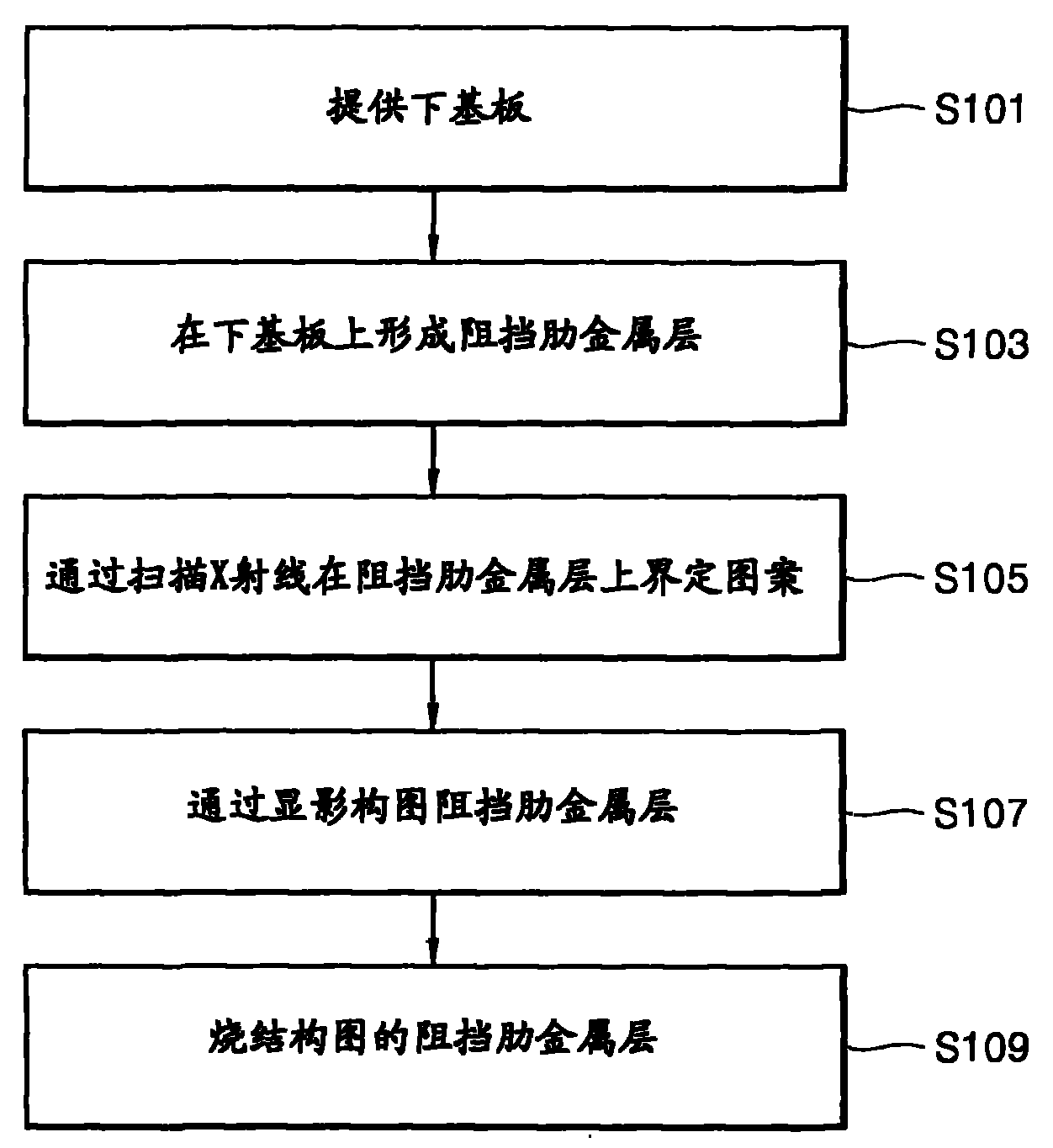
图2是示出根据本发明多个方面的PDP的下面板的制造方法的流程图;2 is a flowchart illustrating a method of manufacturing a lower panel of a PDP according to aspects of the present invention;
图3A至3E是示出图2的方法的详细工艺的垂直截面图;3A to 3E are vertical sectional views showing detailed processes of the method of FIG. 2;
图4是示出作为本发明的对比实例的使用紫外线光刻制造的阻挡肋的垂直截面图;4 is a vertical sectional view showing a barrier rib fabricated using ultraviolet lithography as a comparative example of the present invention;
图5是示出使用根据在图2中示出的方法制造的阻挡肋图案的图;FIG. 5 is a diagram showing barrier rib patterns fabricated using the method shown in FIG. 2;
图6A至6C是示出在不同的曝光条件下制造的阻挡肋的图;6A to 6C are diagrams showing barrier ribs fabricated under different exposure conditions;
图7A至7D是示出根据本发明一方面的PDP的下面板的制造方法的透视图;7A to 7D are perspective views illustrating a method of manufacturing a lower panel of a PDP according to an aspect of the present invention;
图8是示出根据图7A至7D的方法制造的下面板的实例的透视图;8 is a perspective view showing an example of a lower panel manufactured according to the method of FIGS. 7A to 7D;
图9是示出使用根据本发明的多个方面的方法制造的阻挡肋图案的图;9 is a diagram illustrating a pattern of barrier ribs fabricated using a method according to aspects of the present invention;
图10是示出根据本发明的多个方面的下面板的制造方法的图;并且10 is a diagram illustrating a method of manufacturing a lower panel according to aspects of the present invention; and
图11A至11D是示出根据本发明的多个方面的PDP的下面板的制造方法的图。11A to 11D are diagrams illustrating a method of manufacturing a lower panel of a PDP according to aspects of the present invention.
具体实施方式Detailed ways
现将详细描述本发明的实施例,其实例在附图中示出,其中相似的参考标号通篇指示相似的元件。描述下面的实施例以便参考附图解释本发明。但是本发明的各个方面可以以不同的形式实施,并且不应理解为局限于在此提出的实施例。当介绍一层或电极布置或形成于另一层或基板“上”时,该术语意指所述层或电极可以直接形成于另一层或基板上,或者第三层可以布置在其间。另外为了清楚起见,可以夸大层或区的厚度。Embodiments of the invention will now be described in detail, examples of which are illustrated in the accompanying drawings, wherein like reference numerals indicate like elements throughout. The following embodiments are described in order to explain the present invention by referring to the figures. Aspects of the invention may, however, be embodied in different forms and should not be construed as limited to the embodiments set forth herein. When referring to a layer or electrode being disposed or formed "on" another layer or substrate, the term means that the layer or electrode may be formed directly on the other layer or substrate, or that a third layer may be disposed therebetween. Also, the thickness of layers or regions may be exaggerated for clarity.
图2是示出根据本发明多个方面的等离子体显示面板PDP的下面板的制造方法的流程图。参考图2,在此描述了根据本发明多个方面的PDP的下面板的制造方法。首先提供PDP的下基板(S101),在下基板上形成希望厚度的阻挡肋材料层(S103),并且在阻挡肋材料层上扫描X射线从而界定阻挡肋图案(S105)。然后,阻挡肋材料层被显影和构图(S107)。最终,烧结完成的结构(S109),由此完成PDP的下面板。2 is a flowchart illustrating a method of manufacturing a lower panel of a plasma display panel PDP according to aspects of the present invention. Referring to FIG. 2, a method of manufacturing a lower panel of a PDP according to aspects of the present invention is described herein. A lower substrate of the PDP is first provided (S101), a barrier rib material layer of a desired thickness is formed on the lower substrate (S103), and X-rays are scanned on the barrier rib material layer to define a barrier rib pattern (S105). Then, the barrier rib material layer is developed and patterned (S107). Finally, the completed structure is sintered (S109), thereby completing the lower panel of the PDP.
以下,将更详细地按顺序描述上述操作。图3A至3E是示出上述操作的示意工艺图。首先,参考图3A,先前提供的PDP的下基板120布置在工作台S上。下基板120可以是由玻璃材料制成的玻璃基板或由柔性塑料材料制成的柔性基板。此时,如同所示出的,多个电极122可以布置在下基板120上,但是在其它方面可以不同地布置。介电层121布置在下基板120上从而覆盖电极122。电极122布置得相互平行,从而以这样的方式以预定间距分离使得其对应于其中要形成放电空间的区。介电层121可以通过在覆盖电极122的下基板120上整体涂覆介电膏而形成,但不局限于此。根据PDP的希望的结构,可以省略电极122和/或介电层121。例如,在不包括寻址电极的PDP结构内,电极122和介电层121都可以被省略或使用其它方法构造。Hereinafter, the above operations will be described in order in more detail. 3A to 3E are schematic process diagrams illustrating the above-described operations. First, referring to FIG. 3A , the
如上所述使用X射线在提供的下基板120上形成阻挡肋图案。此后,将描述使用X射线光刻的形成阻挡肋图案的方法。首先,参考图3B,在其上形成了电极122和介电层121的下基板120上形成阻挡肋材料层150至厚度H。厚度H相对于介电层121的顶部。阻挡肋材料层150可以由对X射线显示显影特性或显影(例如可以通过X射线光或热固化或在蒸发期间干燥的材料)的材料形成并且因而可以通过显影而构图。此外,阻挡肋材料层150可以通过在下基板120上(或如图所示在介电层121上)涂覆膏状的阻挡肋材料而形成,或者作为替代,在下基板120上层叠片形阻挡肋材料。A barrier rib pattern is formed on the provided
例如,阻挡肋材料层150可以由包括无机微颗粒152的可光固化有机-无机复合材料和多种有机材料151形成,无机微颗粒152是待烧结从而形成阻挡肋的基本玻璃材料。更详细地,无机微颗粒152可以由玻璃料粉末构成,并且无机材料151可以包括使得无机微颗粒152成为膏状的载体、粘合无机微颗粒152的粘合剂、通过光化学反应促进固化的光引发剂等。另外,有机材料151可以包括单体、分散剂或其它材料。For example, the barrier
阻挡肋材料层150的厚度H对应于要形成的阻挡肋的高度。因而,优选阻挡肋材料层150应当形成至足够的厚度。例如,考虑到烧结后阻挡肋的收缩,如果阻挡肋材料层150在烧结前形成至160至180μm的厚度,则在烧结后可以获得具有120至130μm高度的阻挡肋。在形成阻挡肋材料层150至希望的厚度之后,阻挡肋材料层150通过干燥而被固化。当阻挡肋材料层150由膏状的阻挡肋材料形成时需要阻挡肋材料层150的干燥。因而,当无需稳定阻挡肋的形状的附加工艺,例如当阻挡肋材料层150由片形阻挡肋材料形成时,可以省略阻挡肋材料层150的干燥。The thickness H of the barrier
接着,参考图3C,具有预定图案的X射线掩模130布置在所述阻挡肋材料层150上方。此时,X射线掩模130和具有布置在其上的阻挡肋材料层150的下基板120相互垂直对齐。X射线掩模130划分为透射区Wmask和屏蔽区。如同在图3C中所示出的,当X射线掩模130包括透明基板131和吸收器132时,吸收器132至少在透明基板131的表面均匀地构图。这样,透射区Wmask对应于不用吸收器132覆盖的透明基板131的部分,并且屏蔽区对应于用吸收器132覆盖的透明基板131的部分。对应于透射区Wmask的阻挡肋材料层150的部分(图示为150a)在光固化后倾向于形成阻挡肋155,并且对应于屏蔽区的阻挡肋材料层150的部分未被固化并且随后被去除。这里,透明基板131可以由具有良好透射性的材料制成,使得高强度的X射线100可以通过透射区Wmask而透射。为此,透明基板131可以由低原子序数的材料制成以便具有低吸收性。例如,为了制造大尺寸掩模,透明基板131可以由硬玻璃基板或柔性聚酰亚胺膜制成。同时,吸收器132可以形成至例如预定的厚度t,以便不出现穿过屏蔽区的光透射。吸收器132可以由高原子序数的材料制成,例如金(Au)或钨(W),以便增加吸收性。布置在透明基板131表面上的吸收器132可以使用光刻或电镀构图。尽管对于X射线描述了X射线掩模130、透明基板131和吸收器132,但是X射线掩模130、透明基板131和吸收器132不仅局限于此,以便任何形式的电磁辐射可以用于构图阻挡肋材料层150。例如,透明基板131可以对于较高能量的电磁辐射透明并且吸收器132可以阻挡其透射。Next, referring to FIG. 3C , an
接着,X射线100通过X射线掩模130在阻挡肋材料层150上扫描,从而在阻挡肋材料层150上界定希望的图案。该操作可以参考图3D更详细地解释。即当发出X射线100的X射线源(未示出)在X射线掩模130和下基板120被对齐的状态下在一方向上(箭头A)移动时,可以扫描X射线100。作为替代,当X射线掩模130和支撑下基板120的工作台S在一方向上(箭头B)移动时,可以从固定X射线源(未示出)扫描X射线100。方便起见,可以选择最佳方法并且可以涉及X射线源和工作台S的移动。但是,当X射线100和阻挡肋材料层150相互相对运动时在X射线100从阻挡肋材料层150的一侧向对侧扫描方面这两种方法是相同的。曝光于X射线100的阻挡肋材料层150的部分150a通过聚合反应而固化,并且在显影期间留下由此形成阻挡肋155。与此相反,未曝光于X射线100的阻挡肋材料层150的部分未被固化,并且在显影期间被去除,由此界定放电空间。通常,在图案界定中所使用的X射线100可以具有0.01至100的波长但是不仅局限于此。Next, the
出现上述图案界定之后,进行显影。在显影工艺期间,合适的显影剂(例如碱溶液)施加于阻挡肋材料层150,从而选择性地溶解、分散和去除阻挡肋材料层150未固化的部分。在完成显影之后,仅留下被X射线100曝光和固化的阻挡肋材料层150的部分并且形成阻挡肋155,如同在图3E中所示出的。After the pattern definition described above has occurred, development is carried out. During the developing process, a suitable developer, such as an alkaline solution, is applied to the barrier
如同在图3A至图3E中所示出的,由于X射线100的光学特性,具有预定宽度Wrib的阻挡肋155可以被形成得对应于X射线掩模130的透射区Wmask。这样,本发明的优点是可以获得具有均匀宽度,或宽度不在高度方向上变化的精细间距的阻挡肋。As shown in FIGS. 3A to 3E , due to the optical characteristics of the
图4是示出使用UV光线构图的阻挡肋的截面图。参考图4,阻挡肋材料层150包括有机材料151和无机微颗粒152。当照射在阻挡肋材料层150上的UV光线通过阻挡肋材料层150时,其在无机微颗粒152的界面处以宽角度散射并且随后扩散到希望的阻挡肋材料层部分之外进入相邻于希望的阻挡肋材料层部分的阻挡肋材料层150的部分内。曝光于散射光线的阻挡肋材料层150的部分可能被不希望地固化。即对应于掩模的屏蔽区的阻挡肋材料层150的部分也曝光于UV光线。因为这个原因,在高度方向上阻挡肋的宽度W’rib不均匀,而是沿UV光线的光路逐渐增加,即参考图1,阻挡肋材料层150固化从而形成具有在从上基板10至下基板20的方向上增加的宽度的阻挡肋24。FIG. 4 is a cross-sectional view illustrating barrier ribs patterned using UV rays. Referring to FIG. 4 , the barrier
另外,由于光线沿光路被散射,所以UV光线的数量沿UV光线的光路持续地降低。结果,数量不足的UV光线可以施加到最接近于图4的基板120的阻挡肋材料层150的靠近底部的部分内。考虑到这样的问题,当增加UV光线的强度时,散射的强度也增加,并且因而对应于掩模的屏蔽区的阻挡肋材料层150的部分更加曝光于UV光线。与此相反,根据本发明的多个方面,使用在无机微颗粒界面上示出了较少的散射特性的X射线,并且因而可以避免由于光线散射的不可控制的曝光的出现。因此,可以精确地制造具有对应于掩模的透射区的均匀宽度的阻挡肋图案。In addition, the amount of UV light continuously decreases along the light path of the UV light because the light is scattered along the light path. As a result, an insufficient amount of UV rays may be applied into a portion near the bottom of the barrier
根据本发明多个方面所使用的具有短波长的X射线具有足以穿透具有厚的厚度的良好的透射性,并且因而可以贯穿到达阻挡肋材料层的底部。因而,根据本方面的多个方面,可以克服根据所使用的光线的透射性而确定的阻挡肋材料层的厚度的限制。此外,当需要时,通过形成阻挡肋材料层至厚的厚度,可以容易地制造具有高纵横比的阻挡肋(即其中阻挡肋的高度对阻挡肋的宽度的比率高)。另外,由于X射线的高穿透性,可以降低由有机材料和无机微颗粒之间折射率的差别所引起的折射现象,并且因而提高了光线方向性的精度,由此使得可以实现阻挡肋的精细间距的构图。图5示出了使用X射线构图的精细间距的阻挡肋,其中阻挡肋的上宽度是大约14μm。The X-rays having a short wavelength used according to aspects of the present invention have good transmittance enough to penetrate a thick thickness, and thus can penetrate to reach the bottom of the barrier rib material layer. Thus, according to aspects of the present invention, the limitation of the thickness of the barrier rib material layer determined according to the transmittance of light used can be overcome. Furthermore, barrier ribs having a high aspect ratio (ie, wherein the ratio of the height of the barrier rib to the width of the barrier rib is high) can be easily produced by forming the layer of barrier rib material to a thick thickness when desired. In addition, due to the high penetrability of X-rays, the refraction phenomenon caused by the difference in refractive index between the organic material and the inorganic microparticles can be reduced, and thus the precision of the light directionality can be improved, thereby making it possible to realize the barrier rib. Fine-pitch composition. FIG. 5 shows fine-pitch barrier ribs patterned using X-rays, where the upper width of the barrier ribs is about 14 μm.
在阻挡肋材料层内吸收的单位体积的能量数量(曝光剂量,单位:kJ/cm3)与最终获得的阻挡肋结构的精度密切相关。因而,根据本发明的多个方面在将阻挡肋材料层曝光于X射线时,优选(但不必须)通过数量计算精确地控制施加到阻挡肋材料层的X射线的剂量。考虑到X射线的贯穿深度和阻挡肋材料层的X射线吸收性,施加到阻挡肋材料层的X射线的剂量可以通过控制曝光条件(例如X射线的强度,曝光时间)而优化。图6A至6C是示出在不同曝光条件下制造的阻挡肋的图。如果曝光时间太短,则由于阻挡肋材料层由于缺少曝光而未足够地固化,所以阻挡肋未能正确地形成,如同在图6A中所示出的。与此相反,如果曝光时间太长,如同在图6C中所示出的,则在完成的阻挡肋内产生缺陷(例如空腔或裂缝),并且对应于X射线掩模的屏蔽区的阻挡肋材料层的部分也曝光于X射线,由此导致对应于X射线掩模的屏蔽区的阻挡肋材料层的部分的固化。但是,通过合适的曝光时间制造的阻挡肋具有光滑的表面,如同在图6B中所示出的。The amount of energy per unit volume absorbed in the barrier rib material layer (exposure dose, unit: kJ/cm 3 ) is closely related to the precision of the finally obtained barrier rib structure. Thus, when exposing the layer of barrier rib material to X-rays according to aspects of the present invention, it is preferable, but not necessary, to precisely control the dose of X-rays applied to the layer of barrier rib material by quantitative calculations. The dose of X-rays applied to the barrier rib material layer can be optimized by controlling the exposure conditions (eg X-ray intensity, exposure time) in consideration of the penetration depth of the X-rays and the X-ray absorption of the barrier rib material layer. 6A to 6C are diagrams showing barrier ribs fabricated under different exposure conditions. If the exposure time is too short, the barrier ribs are not properly formed because the layer of barrier rib material is not sufficiently cured due to lack of exposure, as shown in Figure 6A. On the contrary, if the exposure time is too long, as shown in FIG. 6C, defects (such as cavities or cracks) are generated in the completed barrier ribs, and the barrier ribs corresponding to the shielding regions of the X-ray mask Portions of the layer of material are also exposed to X-rays, thereby causing curing of portions of the layer of barrier rib material corresponding to shielded regions of the X-ray mask. However, the barrier ribs fabricated with a suitable exposure time have a smooth surface, as shown in FIG. 6B.
再次参考图3A至3E,烧结通过上述图案界定以及显影所获得的阻挡肋材料层图案。为此,阻挡肋材料层图案被加热到接近在阻挡肋材料层图案中所包含的无机微颗粒152(例如玻璃料)的熔点的高温,使得无机微颗粒152被熔化和烧结,并且同时,去除阻挡肋材料层图案中所包含的有机材料151。Referring again to FIGS. 3A to 3E , the barrier rib material layer pattern obtained through the above pattern definition and development is sintered. For this, the barrier rib material layer pattern is heated to a high temperature close to the melting point of the inorganic fine particles 152 (eg, glass frit) contained in the barrier rib material layer pattern, so that the inorganic
根据本发明的多个方面,示出了使用X射线光刻的阻挡肋的形成。但是,如果阻挡肋材料层可以使用X射线构图,则基于X射线的阻挡肋的形成方法不仅局限于上述方法,并且所述技术原理可以应用于根据本发明多个方面的各种方法。例如,可以根据阻挡肋图案控制X射线的光路替代使用曝光掩模。这样,可以在阻挡肋材料层上界定希望的图案。这可以通过以在双轴方向上可移动的X-Y表操纵X射线枪而实现。According to aspects of the invention, the formation of barrier ribs using X-ray lithography is shown. However, if the barrier rib material layer can be patterned using X-rays, the formation method of the X-ray based barrier ribs is not limited to the above methods, and the technical principles can be applied to various methods according to aspects of the present invention. For example, instead of using an exposure mask, an optical path of X-rays may be controlled according to a barrier rib pattern. In this way, a desired pattern can be defined on the layer of barrier rib material. This can be achieved by manipulating the X-ray gun with an X-Y table movable in a biaxial direction.
图7A至7D是示出根据本发明一方面的PDP的下面板的制造方法的透视图。如上所述,在阻挡肋材料层上使用X射线界定希望的图案,但是所谓的阶梯阻挡肋图案,即其中阻挡肋的不同位置具有不同高度的阻挡肋,使用两个操作形成:第一图案界定和第二图案界定。7A to 7D are perspective views illustrating a method of manufacturing a lower panel of a PDP according to an aspect of the present invention. As mentioned above, X-rays are used to define the desired pattern on the layer of barrier rib material, but so-called stepped barrier rib patterns, i.e. barrier ribs in which different positions of the barrier ribs have different heights, are formed using two operations: the first pattern defines and the second pattern defined.
以下,将更详细地描述本发明的多个方面。首先,参考图7A,事先提供的PDP的下基板120放置在工作台S上。此时,在下基板120上形成多个电极122和布置以覆盖电极122的介电层121,但是无需局限于此。然后,在下基板120上形成第一阻挡肋材料层150’。例如,第一阻挡肋材料层150’可以通过涂覆包括无机微颗粒和各种功能的有机材料的光敏膏而形成至预定的厚度ho。这里,第一阻挡肋材料层150’的厚度ho对应于将形成的阶梯阻挡肋中具有相对较低高度的第一阻挡肋的高度。然后,第一阻挡肋材料层150’被干燥。根据第一阻挡肋材料层150’的材料的物理特性,第一阻挡肋材料层150’的干燥可以被省略。例如,如果阻挡肋材料片粘附于下基板,则无需干燥。Hereinafter, various aspects of the present invention will be described in more detail. First, referring to FIG. 7A, the
接着,参考图7B,具有预定图案的X射线掩模130在其上形成了第一阻挡肋材料层150’的下基板120的上方对齐。X射线掩模130可以是其中在透明基板131的表面上构图了吸收器132的掩模。这里,吸收器132界定屏蔽X射线的屏蔽区,并且未用吸收器132覆盖的透明基板131的部分界定透射X射线的透射区。X射线掩模130可以被设计为具有在一方向(例如x轴方向)被条形构图的透射区。Next, referring to FIG. 7B , an
然后,在第一阻挡肋材料层150’上使用X射线掩模130界定希望的图案(第一图案界定)。此时,对应于X射线掩模130的透射区的第一阻挡肋材料层150’的部分150b曝光于X射线100,并且通过聚合反应而固化。对应于X射线掩模130的屏蔽区的第一阻挡肋材料层150’的部分未被固化。同时,在该操作中,当发出X射线100的X射线源(未示出)在其中X射线掩模130和下基板120固定地对齐的条件下在一方向(例如在x轴方向,或箭头A)移动时,可以扫描X射线100,或者作为替代,当X射线掩模130和支撑下基板120的工作台S在一方向(例如x轴方向,或箭头B)移动时,X射线100可以从固定X射线源(未示出)扫描。Then, a desired pattern is defined on the first barrier rib material layer 150' using the X-ray mask 130 (first pattern definition). At this time, the
当如上所述且如图7C所示完成第一图案界定时,第二阻挡肋材料层150”在具有厚度ho的第一阻挡肋材料层150’上被涂覆以厚度Δh。因而,包括第一和第二阻挡肋材料层150’和150”的阻挡肋材料层150在下基板120上形成至厚度h(ho+Δh)。此时,阻挡肋材料层150的厚度h对应于阶梯阻挡肋之中具有相对较高高度的第二阻挡肋的高度。如上所述形成第二阻挡肋材料层150”之后,如果需要,可以干燥阻挡肋材料层150。When the first pattern definition is completed as described above and as shown in FIG. The barrier
接着,参考图7D,X射线掩模130’在阻挡肋材料层150上方被对齐。X射线掩模130’可以是其中吸收器132’在透明基板131’的表面上被构图的掩模。X射线掩模130’可以被设计为具有在一方向(例如在z轴方向)上被条形构图的透射区。透射区可以延伸,从而与在上述第一图案的界定中所使用的X射线掩模130的透射区交叉。Next, referring to FIG. 7D , an X-ray mask 130' is aligned over the
再一次,使用X射线掩模130’在阻挡肋材料层150上界定希望的图案(第二图案界定)。此时,对应于X射线掩模130’的透射区的阻挡肋材料层150的部分150c曝光于X射线100并且通过聚合反应而固化。此时,通过第二图案界定固化的图案可以与通过第一图案界定固化的图案重叠。同时,在该操作中,当发出X射线100的X射线源(未示出)在X射线掩模130’和下基板120固定地对齐的状态下在一方向(例如在z轴方向,或箭头A’)移动时,可以扫描X射线100,或者作为替代,当X射线掩模130’和支撑下基板120的工作台S在一方向上(例如在z轴方向,或箭头B’)移动时,X射线100可以从固定的X射线源(未示出)扫描。尽管作为x轴和z轴方向描述和图示了方向,但是方向不仅局限于此,使得x轴和z轴方向无需垂直而仅需要交叉或延伸至相交。此外,可以应用第三和/或第四等X射线图案界定工艺以进一步界定具有不同高度的阻挡肋,从而获得多阶梯的阻挡肋和具有不同高度的不同图案的阻挡肋。Again, the desired pattern is defined on the barrier
如上所述,如上所述进行两步X射线图案界定工艺之后,阻挡肋材料层150被显影和烧结,由此获得如同在图8中所示出的阶梯阻挡肋124。参考图8,阶梯阻挡肋124包括延伸以相互交叉并且分别具有高度h’o和h’的第一阻挡肋124a和第二阻挡肋124b,使得第一阻挡肋124a和第二阻挡肋124b从下介电层121延伸至不同的高度,其中下介电层121布置在下基板120上从而覆盖电极122。图9是示出根据上述方法制造的阶梯阻挡肋图案的图。As mentioned above, after performing the two-step X-ray pattern definition process as described above, the barrier
根据本发明的多个方面,示出了使用X射线光刻的阻挡肋的形成,但是并不局限于此。例如,通过在预定的光路内设置X射线的输出,可以实现选择性的曝光。更具体地,例如使用X-Y表,通过使用沿控制路径从X射线枪引导X射线的驱动器构图阻挡肋材料层。According to aspects of the present invention, the formation of barrier ribs using X-ray lithography is shown, but not limited thereto. For example, selective exposure can be achieved by placing the output of X-rays within a predetermined optical path. More specifically, the layer of barrier rib material is patterned by using an actuator that directs X-rays from an X-ray gun along a controlled path, for example using an X-Y table.
现将参考图10描述根据本发明多个方面的PDP的下面板的制造方法。根据在图10中的本发明的多个方面,无需X射线掩模覆盖阻挡肋材料层的整个面积,而是将X射线掩模放置在X射线的光路内,并且具有仅足以覆盖受到X射线照射的阻挡肋材料层的部分的小面积。即,参考图10,涂覆以阻挡肋材料层150的下基板120放置于在一方向上可移动地安装的工作台S上,并且X射线枪(未示出)和X射线掩模230固定地安装在工作台S上方。此时,X射线掩模230可以包括透明基板231和粘附在透明基板231上的吸收器232从而界定透射区和屏蔽区。通过将X射线掩模230放置在X射线100的光路内,预定的X射线100束可以在阻挡肋材料层150上扫描。A method of manufacturing a lower panel of a PDP according to aspects of the present invention will now be described with reference to FIG. 10 . According to aspects of the invention in FIG. 10 , the x-ray mask is not required to cover the entire area of the layer of barrier rib material, but the x-ray mask is placed within the optical path of the x-rays and has only enough coverage A small area of the portion of the layer of barrier rib material that is irradiated. That is, referring to FIG. 10 , the
当其上布置了下基板120的工作台S移动,使得下基板120在一方向上以预定速度运动时,X射线100通过X射线掩模230在阻挡肋材料层150上扫描。因而当以预定速度相对于固定的X射线枪移动时,涂覆在下基板120上的阻挡肋材料层150逐渐暴露于X射线100。即当阻挡肋材料层150相对于从固定X射线枪发出的X射线100移动时,X射线100从阻挡肋材料层150的一侧向对侧扫描。此时,包括阻挡肋材料层150的工作台S移动的预定速度对应于X射线100的扫描速度,并且确定X射线100对于阻挡肋材料层150的曝光剂量。因而,优选考虑到X射线100的穿透深度和阻挡肋材料层150的吸收性而优化包括阻挡肋材料层150的工作台S移动的预定速度。例如,当阻挡肋材料层150由负型材料形成时,曝光于X射线100的阻挡肋材料层150的部分150d通过聚合反应而固化。阻挡肋材料层150的曝光部分150d在显影期间被留下从而最终形成阻挡肋。When the stage S on which the
根据本发明的多个方面,形成X射线掩模,从而具有至少覆盖X射线的光路并且比阻挡肋材料层的面积小的面积。因而当获得与上述相同的曝光效果时,可以实现掩模制造成本的下降。结果,降低了PDP的制造成本,由此提高了成本和价格的竞争性。具体地,对于大尺寸(例如大于或等于40英寸)的显示器,实现了成本的显著降低。According to aspects of the present invention, the X-ray mask is formed so as to have an area covering at least an optical path of X-rays and smaller than that of the barrier rib material layer. Thus, when the same exposure effect as above is obtained, reduction in mask manufacturing cost can be achieved. As a result, the manufacturing cost of the PDP is reduced, thereby improving cost and price competitiveness. In particular, for displays of large size (eg, greater than or equal to 40 inches), significant cost reductions are achieved.
图11A至图11D是示出根据本发明的多个方面的PDP的下面板的制造方法的工艺图。在图11A至11D中示出的本发明的多个方面还提供了一种使用两个操作,即第一图案界定和第二图案界定而形成阶梯阻挡肋图案的方法。此外,根据在图11A至11D中所示出的本发明的多个方面,使用较小的X射线掩模进行多个图案界定由此降低掩模的制造成本。11A to 11D are process diagrams illustrating a method of manufacturing a lower panel of a PDP according to aspects of the present invention. Aspects of the invention shown in FIGS. 11A to 11D also provide a method of forming a stepped barrier rib pattern using two operations, first pattern definition and second pattern definition. Furthermore, according to aspects of the invention shown in FIGS. 11A-11D , a smaller X-ray mask is used for multiple pattern definitions thereby reducing the manufacturing cost of the mask.
首先,参考图11A,预先提供的PDP的下基板120布置在工作台S上,并且第一阻挡肋材料层150’以厚度ho涂覆于下基板120上。这里第一阻挡肋材料层150’的厚度ho对应于待形成的阶梯阻挡肋中具有相对低的高度的第一阻挡肋的高度。可以选择性地干燥第一阻挡肋材料层150’。First, referring to FIG. 11A , the
接着,参考图11B,X射线掩模230被制备并且放置在X射线100的光路内。X射线掩模230可以包括透明基板231和吸收器232从而分别界定透射区和屏蔽区,并且X射线掩模230的透射区可以设计为在一方向(例如在示出的x轴方向)上延伸。X射线掩模230置于X射线100的光路内并且具有小的面积从而仅覆盖有可能曝光于X射线100的第一阻挡肋材料层150’的部分。因而,可以降低X射线掩模230的制造成本,由此降低PDP的制造成本并且增加PDP的价格竞争性。Next, referring to FIG. 11B , an
接着,使用X射线掩模230在第一阻挡肋材料层150’上界定希望的图案(第一图案界定)。即用第一阻挡肋材料层150’涂覆的下基板120布置在工作台S上,并且X射线枪(未示出)和X射线掩模固定地布置于工作台S上方。此时,X射线掩模230置于X射线100的光路内。当支撑下基板120的工作台S移动使得下基板120以预定速度在一方向(例如在x轴方向)上运动时, X射线100扫描。这里,下基板120的移动方向平行于X射线掩模230的透射区的延伸方向(例如x轴方向)。当第一阻挡肋材料层150’以预定速度相对于从固定的X射线源(未示出)发出的X射线100移动时,X射线100从第一阻挡肋材料层150’的一侧向对侧扫描。随着X射线100被扫描,对应于X射线掩模230的透射区的第一阻挡肋材料层150’的部分150e曝光于X射线100并且通过聚合反应而固化。对应于X射线掩模230的屏蔽区的第一阻挡肋材料层150’的部分保持原样直至进行第二图案界定工艺之后。Next, a desired pattern is defined on the first barrier rib material layer 150' using the X-ray mask 230 (first pattern definition). That is, the
完成第一图案界定工艺之后,第二阻挡肋材料层150”以Δh的厚度涂覆于具有厚度ho的第一阻挡肋材料层150’上,如同在图11C中所示出的。因而,包括第一和第二阻挡肋材料层150’和150”的阻挡肋材料层150以h(ho+Δh)的厚度在下基板120上形成。此时,阻挡肋材料层150的厚度h对应于阶梯阻挡肋之中具有相对较高的高度的第二阻挡肋的高度。形成第二阻挡肋材料层150”之后,可以干燥阻挡肋材料层150。After completing the first pattern defining process, a second barrier
接着,参考图11D,提供X射线掩模230’并且置于X射线100的光路内。尽管并非在所有方面都需要,但是X射线掩模230’可以包括透明基板231’和布置在透明基板231’上的吸收器232’,从而界定X射线掩模230’在一方向(例如在示出的z轴方向)上的透射区。X射线掩模230’的透射区可以与在第一图案界定工艺中使用的X射线掩模230的透射区交叉。X射线掩模230’具有小的面积从而仅覆盖X射线照射之下的阻挡肋材料层150的部分或掩模整个X射线照射的光路,由此减小掩模的制造成本。Next, referring to FIG. 11D , an X-ray mask 230' is provided and placed within the optical path of the
接着,使用X射线掩模230’在阻挡肋材料层150上界定希望的图柔。支撑阻挡肋材料层150的下基板120布置在沿至少一方向(例如在z轴方向)上可移动地安装的工作台S上,并且X射线枪(未示出)和X射线掩模230’固定地安装在下基板120上方并且以预定距离与下基板120分离。此时,X射线掩模230’在X射线100的光路上对齐。当其上布置了下基板120的工作台S在一方向(例如z轴方向)上工作时,X射线100在阻挡肋材料层150上扫描。当阻挡肋材料层150对于X射线100相对移动时,从固定的X射线枪发出的X射线100可以从阻挡肋材料层150的一侧向对侧扫描。随着X射线100被扫描,曝光于X射线100的阻挡肋材料层150的部分150f通过聚合反应而固化。此时,通过第二图案界定工艺而被曝光和固化的部分150f可以与通过第一图案界定工艺而曝光和固化的部分150e重叠。Next, a desired pattern is defined on the barrier
当显影和烧结如上所述界定了图案的阻挡肋材料层150时,阻挡肋材料层150的无机微颗粒相互熔合从而最终形成阶梯的阻挡肋(见图8的124)。阶梯的阻挡肋包括延伸得相互交叉并且具有不同高度(见图8的h’o和h’)的第一阻挡肋(见图8的124a)和第二阻挡肋(见图8的124b),使得第一阻挡肋和第二阻挡肋相互成垂直的阶梯。When developing and sintering the barrier
根据本发明的多个方面,可以使用具有预定光学特性的X射线在阻挡肋材料层上精确地界定希望的图案,并且因而可以以高精度实现精细间距和高分辨率的阻挡肋的构图。此外,在图案界定中所使用的X射线具有高穿透效率,使得X射线可以固化甚至最接近于基板的阻挡肋材料。因而,为了以高纵横比制造阻挡肋,可以以降低的工艺限制将光敏膏制涂覆到希望的厚度。According to aspects of the present invention, a desired pattern can be precisely defined on a barrier rib material layer using X-rays having predetermined optical characteristics, and thus fine-pitch and high-resolution patterning of barrier ribs can be achieved with high precision. Furthermore, the X-rays used in pattern definition have high penetration efficiency so that the X-rays can cure barrier rib materials even closest to the substrate. Thus, in order to fabricate barrier ribs with a high aspect ratio, the photosensitive paste can be applied to a desired thickness with reduced process constraints.
此外根据本发明的多个方面,在包含两种或多种不同成分的阻挡肋材料内X射线示出了相对低的散射特性。因而,当选择阻挡肋材料时,无需考虑阻挡肋材料的其它光学特性(例如折射率),由此与使用特殊阻挡肋材料的常规UV光刻相比,降低了制造成本。Furthermore, according to aspects of the present invention, X-rays exhibit relatively low scattering characteristics within barrier rib materials comprising two or more different compositions. Thus, other optical properties of the barrier rib material, such as the index of refraction, need not be considered when selecting the barrier rib material, thereby reducing manufacturing costs compared to conventional UV lithography using special barrier rib materials.
另外,根据本发明的多个方面,当使用X射线掩模进行图案界定时,根据X射线照射的面积,可以减小X射线掩模的尺寸,由此降低制造成本和增加价格的竞争性。具体地,当制造大尺寸(例如大于或等于40英寸)的等离子体显示面板时,可以显著地降低制造成本。In addition, according to aspects of the present invention, when an X-ray mask is used for pattern definition, the size of the X-ray mask can be reduced according to the area irradiated by X-rays, thereby reducing manufacturing costs and increasing price competitiveness. In particular, when manufacturing large-sized (for example, greater than or equal to 40 inches) plasma display panels, the manufacturing cost can be significantly reduced.
尽管示出和描述了本发明的一些实施例,但是本领域的技术人员应当理解,在不偏离本发明的原理和精神的前提下可以对这些该实施例进行变更,本发明的范围在所附权利要求及其等同物中界定。Although some embodiments of the present invention have been shown and described, those skilled in the art should understand that these embodiments can be changed without departing from the principle and spirit of the present invention, and the scope of the present invention is set forth in the appended defined in the claims and their equivalents.
本申请要求2006年12月29日向韩国知识产权局提交的韩国专利申请第2006-138906号和韩国专利申请第2006-138907号的优先权,其整个内容引用在此处作为参考。This application claims priority from Korean Patent Application No. 2006-138906 and Korean Patent Application No. 2006-138907 filed with the Korean Intellectual Property Office on December 29, 2006, the entire contents of which are incorporated herein by reference.
Claims (20)
Applications Claiming Priority (3)
| Application Number | Priority Date | Filing Date | Title |
|---|---|---|---|
| KR1020060138906A KR100838074B1 (en) | 2006-12-29 | 2006-12-29 | Method for manufacturing bottom plate for plasma display panel using X-ray |
| KR138906/06 | 2006-12-29 | ||
| KR138907/06 | 2006-12-29 |
Publications (1)
| Publication Number | Publication Date |
|---|---|
| CN101221873A true CN101221873A (en) | 2008-07-16 |
Family
ID=39631622
Family Applications (1)
| Application Number | Title | Priority Date | Filing Date |
|---|---|---|---|
| CNA2007103052027A Pending CN101221873A (en) | 2006-12-29 | 2007-12-29 | Method of manufacturing lower panel of plasma display panel using X-rays |
Country Status (2)
| Country | Link |
|---|---|
| KR (1) | KR100838074B1 (en) |
| CN (1) | CN101221873A (en) |
Families Citing this family (1)
| Publication number | Priority date | Publication date | Assignee | Title |
|---|---|---|---|---|
| KR101077431B1 (en) * | 2009-08-11 | 2011-10-27 | 경북대학교 산학협력단 | Fabrication method of metallic electrodes using X-ray lithography process, metallic electrodes by the method and plasma display panel including the same |
Family Cites Families (4)
| Publication number | Priority date | Publication date | Assignee | Title |
|---|---|---|---|---|
| KR100459890B1 (en) * | 1999-05-26 | 2004-12-03 | 삼성에스디아이 주식회사 | Method for fabricating a barrier rib of plasma display panel |
| KR100349610B1 (en) * | 1999-06-30 | 2002-08-21 | 전자부품연구원 | Method for manufacturing partitions of plasma display pannel |
| JP2002042655A (en) | 2000-07-24 | 2002-02-08 | Nippon Hoso Kyokai <Nhk> | Method for producing spacer for high definition display panel, and display device using the same |
| JP2004047299A (en) | 2002-07-12 | 2004-02-12 | Matsushita Electric Ind Co Ltd | Method of forming partition |
-
2006
- 2006-12-29 KR KR1020060138906A patent/KR100838074B1/en not_active Expired - Fee Related
-
2007
- 2007-12-29 CN CNA2007103052027A patent/CN101221873A/en active Pending
Also Published As
| Publication number | Publication date |
|---|---|
| KR100838074B1 (en) | 2008-06-16 |
Similar Documents
| Publication | Publication Date | Title |
|---|---|---|
| KR100736345B1 (en) | Method of preparing barrier rib master pattern for barrier rib transfer and method of forming barrier ribs | |
| US6713959B1 (en) | Plasma display panel and method for producing the same | |
| JP3684603B2 (en) | Method for manufacturing plasma display panel | |
| CN1482647A (en) | Plasma display panel including barrier ribs and method of manufacturing barrier ribs | |
| CN101221873A (en) | Method of manufacturing lower panel of plasma display panel using X-rays | |
| EP1939919B1 (en) | Method of manufacturing lower panel for plasma display panel using X-Rays | |
| KR100838075B1 (en) | Method for manufacturing bottom plate for plasma display panel using X-ray | |
| JP3565905B2 (en) | Plasma display panel and manufacturing method thereof | |
| JP3573022B2 (en) | Method for forming dielectric and barrier ribs of plasma display panel | |
| KR100630415B1 (en) | Manufacturing Method Of Plasma Display Panel | |
| JP4539112B2 (en) | Method for manufacturing plasma display panel | |
| JP2004342348A (en) | Method for manufacturing plasma display panel | |
| CN1150499C (en) | Manufacturing method of plasma display panel | |
| JP2009146682A (en) | Method for manufacturing plasma display panel | |
| US20070232038A1 (en) | Method of manufacturing plasma display panel and photomask to be used in the method | |
| JP2006066148A (en) | Panel for planar display device | |
| JP2003197111A (en) | Plasma display panel and method of manufacturing the plasma display panel | |
| KR100672387B1 (en) | Top plate manufacturing method of plasma display panel | |
| JP4386244B2 (en) | Panel display device manufacturing method and display panel manufacturing device | |
| KR100829252B1 (en) | Manufacturing method of partition sheet, partition manufacturing method of plasma display panel and plasma display panel | |
| JP2003142007A (en) | Display device | |
| KR20070055342A (en) | Plasma display panel | |
| JPH11213889A (en) | Planar display substrate forming board, and manufacture of planar display substrate using the board | |
| KR20080024348A (en) | Manufacturing Method Of Plasma Display Panel | |
| JPH10269936A (en) | Gas discharge display panel and method of manufacturing the same |
Legal Events
| Date | Code | Title | Description |
|---|---|---|---|
| C06 | Publication | ||
| PB01 | Publication | ||
| C10 | Entry into substantive examination | ||
| SE01 | Entry into force of request for substantive examination | ||
| C02 | Deemed withdrawal of patent application after publication (patent law 2001) | ||
| WD01 | Invention patent application deemed withdrawn after publication |
Open date: 20080716 |