CN101156159B - Digital predistortion system and method for high efficiency transmitter - Google Patents
Digital predistortion system and method for high efficiency transmitter Download PDFInfo
- Publication number
- CN101156159B CN101156159B CN2005800066277A CN200580006627A CN101156159B CN 101156159 B CN101156159 B CN 101156159B CN 2005800066277 A CN2005800066277 A CN 2005800066277A CN 200580006627 A CN200580006627 A CN 200580006627A CN 101156159 B CN101156159 B CN 101156159B
- Authority
- CN
- China
- Prior art keywords
- predistortion
- digital
- signal
- sample
- circuit
- Prior art date
- Legal status (The legal status is an assumption and is not a legal conclusion. Google has not performed a legal analysis and makes no representation as to the accuracy of the status listed.)
- Expired - Fee Related
Links
Images


Classifications
-
- H—ELECTRICITY
- H03—ELECTRONIC CIRCUITRY
- H03F—AMPLIFIERS
- H03F1/00—Details of amplifiers with only discharge tubes, only semiconductor devices or only unspecified devices as amplifying elements
- H03F1/32—Modifications of amplifiers to reduce non-linear distortion
- H03F1/3241—Modifications of amplifiers to reduce non-linear distortion using predistortion circuits
- H03F1/3294—Acting on the real and imaginary components of the input signal
-
- H—ELECTRICITY
- H03—ELECTRONIC CIRCUITRY
- H03F—AMPLIFIERS
- H03F1/00—Details of amplifiers with only discharge tubes, only semiconductor devices or only unspecified devices as amplifying elements
- H03F1/32—Modifications of amplifiers to reduce non-linear distortion
-
- H—ELECTRICITY
- H03—ELECTRONIC CIRCUITRY
- H03F—AMPLIFIERS
- H03F1/00—Details of amplifiers with only discharge tubes, only semiconductor devices or only unspecified devices as amplifying elements
- H03F1/32—Modifications of amplifiers to reduce non-linear distortion
- H03F1/3241—Modifications of amplifiers to reduce non-linear distortion using predistortion circuits
- H03F1/3258—Modifications of amplifiers to reduce non-linear distortion using predistortion circuits based on polynomial terms
-
- H—ELECTRICITY
- H04—ELECTRIC COMMUNICATION TECHNIQUE
- H04K—SECRET COMMUNICATION; JAMMING OF COMMUNICATION
- H04K1/00—Secret communication
- H04K1/02—Secret communication by adding a second signal to make the desired signal unintelligible
-
- H—ELECTRICITY
- H03—ELECTRONIC CIRCUITRY
- H03F—AMPLIFIERS
- H03F2201/00—Indexing scheme relating to details of amplifiers with only discharge tubes, only semiconductor devices or only unspecified devices as amplifying elements covered by H03F1/00
- H03F2201/32—Indexing scheme relating to modifications of amplifiers to reduce non-linear distortion
- H03F2201/3209—Indexing scheme relating to modifications of amplifiers to reduce non-linear distortion the amplifier comprising means for compensating memory effects
-
- H—ELECTRICITY
- H03—ELECTRONIC CIRCUITRY
- H03F—AMPLIFIERS
- H03F2201/00—Indexing scheme relating to details of amplifiers with only discharge tubes, only semiconductor devices or only unspecified devices as amplifying elements covered by H03F1/00
- H03F2201/32—Indexing scheme relating to modifications of amplifiers to reduce non-linear distortion
- H03F2201/3224—Predistortion being done for compensating memory effects
-
- H—ELECTRICITY
- H04—ELECTRIC COMMUNICATION TECHNIQUE
- H04L—TRANSMISSION OF DIGITAL INFORMATION, e.g. TELEGRAPHIC COMMUNICATION
- H04L25/00—Baseband systems
- H04L25/02—Details ; arrangements for supplying electrical power along data transmission lines
- H04L25/03—Shaping networks in transmitter or receiver, e.g. adaptive shaping networks
- H04L25/03006—Arrangements for removing intersymbol interference
- H04L25/03343—Arrangements at the transmitter end
Landscapes
- Physics & Mathematics (AREA)
- Engineering & Computer Science (AREA)
- Nonlinear Science (AREA)
- Power Engineering (AREA)
- Algebra (AREA)
- General Physics & Mathematics (AREA)
- Mathematical Analysis (AREA)
- Mathematical Optimization (AREA)
- Pure & Applied Mathematics (AREA)
- Computer Networks & Wireless Communication (AREA)
- Signal Processing (AREA)
- Amplifiers (AREA)
Abstract
Description
相关申请信息Relevant application information
本申请要求2004年3月3日提交的临时申请序列号No.60/549,789的优先权,该申请的公开内容整体地在此引用以供参考。This application claims priority to Provisional Application Serial No. 60/549,789, filed March 3, 2004, the disclosure of which is incorporated herein by reference in its entirety.
发明领域Field of Invention
本发明涉及高效率、高功率RF放大器的预失真线性化和相关的系统与方法。The present invention relates to predistortion linearization of high efficiency, high power RF amplifiers and related systems and methods.
背景、现有技术和相关信息Background, prior art and related information
现代无线通信系统利用具有宽的带宽和时变包络的、频谱有效的数字调制信号。数字调制的包络幅度的变化会生成发射机的输出端处的失真分量,该失真分量是由RF放大电路的固有非线性造成的。放大器失真产生输入信号的频谱扩张(“频谱再生长”),这造成对相邻信道中的通信的干扰。邻道干扰(ACI)是由管理机构(FCC、ETSI、ITU)严格控制的、非常不期望的现象。除了频谱再生长以外,放大器非线性还产生带内失真(即,在调制的输入信号的带宽内的失真分量),这恶化了所传送信号的完整性,以及在接收机端导致高的误码率(BER)。常规的RF放大器(AB类)中的非线性是相对较小的(对于等于该调制峰值平均功率比(PAR)的输出回退(output back offs,OBO)低于载波水平近似40dB的失真)。为这样的轻微非线性性状付出的代价是差的效率,即,受限的DC到RF功率转换性能。高效率放大是特别希望的,因为它改进了系统可靠性(更长的平均故障前时间(MTBF)),简化了热学管理,减小了放大器尺寸(更低的硅需要),和降低了基站的运行和拥有花费。另一方面,高效率放大器(例如Doherty放大器设计)比AB类设计展现了更加非线性的性状(低于载波水平约29dB处或载波水平之下少于29dB的失真)。Modern wireless communication systems utilize spectrally efficient digitally modulated signals with wide bandwidths and time-varying envelopes. Variations in the envelope amplitude of the digital modulation generate distortion components at the output of the transmitter, which are caused by the inherent nonlinearity of the RF amplification circuit. Amplifier distortion produces spectral expansion ("spectral regrowth") of the input signal, which causes interference with communications in adjacent channels. Adjacent channel interference (ACI) is a highly undesirable phenomenon strictly controlled by regulatory agencies (FCC, ETSI, ITU). In addition to spectral regrowth, amplifier nonlinearities also generate in-band distortion (i.e., distortion components within the bandwidth of the modulated input signal), which degrades the integrity of the transmitted signal and leads to high bit errors at the receiver rate (BER). Nonlinearities in conventional RF amplifiers (class AB) are relatively small (distortion of approximately 40dB below carrier level for output back offs (OBO) equal to the modulation peak-to-average power ratio (PAR)). The price paid for such slightly non-linear behavior is poor efficiency, ie limited DC to RF power conversion performance. High-efficiency amplification is particularly desirable because it improves system reliability (longer mean time before failure (MTBF)), simplifies thermal management, reduces amplifier size (lower silicon requirements), and reduces base station operating and owning costs. On the other hand, high efficiency amplifiers (such as Doherty amplifier designs) exhibit more nonlinear behavior (distortion at or below 29dB below carrier level) than class AB designs.
线性化的一个简单方法是增加OBO的水平,以便通过扩展放大器的线性工作范围而减小输出失真。这种技术可以被成功地应用来增强AB类放大器的线性度。不幸地是,由于较高的OBO水平引起的RF输出功率的减小,这也造成效率的严重损失。另一方面,高效率放大器典型地不能通过简单提高OBO而被线性化,且需要更先进的线性化技术。一种非常确实(well established)的技术使用笛卡儿(或极)反馈来最小化放大器的输出失真。反馈线性化对于窄的信号带宽可以是有效的,但当需要宽的带宽操作时(例如,多载波WCDMA),由于与环路动态特性有关的输入输出稳定性限制,它只具有非常有限的失真校正能力。所以,反馈将不足以使宽的带宽、高效率的发射机线性化。另一个技术-前馈-是基于放大器失真的加性后校正,典型地采用双环路结构,以估值在第一(载波消除)环路中的放大器的输出失真,然后经由在第二(失真消除)环路中的RF辅助或“误差”放大器,把经适当定相和缩放的失真估值注入到“主”放大器的输出。前馈线性化系统不受反馈线性化器的带宽限制且是无条件地稳定的。然而,且尽管具有宽的带宽失真校正能力,由于误差放大器的DC功率消耗和失真消除环路的相位对准所需要的、在主放大器输出端处有损延迟单元的存在,前馈系统通常具有低的效率。A simple method of linearization is to increase the level of OBO to reduce output distortion by extending the amplifier's linear operating range. This technique can be successfully applied to enhance the linearity of class AB amplifiers. Unfortunately, this also results in a severe loss of efficiency due to the reduction in RF output power caused by higher OBO levels. On the other hand, high efficiency amplifiers typically cannot be linearized by simply increasing the OBO and require more advanced linearization techniques. A well established technique uses Cartesian (or polar) feedback to minimize output distortion of the amplifier. Feedback linearization can be effective for narrow signal bandwidths, but when wide bandwidth operation is required (e.g., multi-carrier WCDMA), it has only very limited distortion due to input-output stability limitations related to loop dynamics Calibration ability. Therefore, feedback will not be sufficient to linearize a wide bandwidth, high efficiency transmitter. Another technique - feed-forward - is based on additive post-correction of amplifier distortion, typically using a dual-loop configuration, to estimate the output distortion of the amplifier in the first (carrier cancellation) loop, then via the second (distortion Elimination) The RF auxiliary or "error" amplifier in the loop injects an appropriately phased and scaled distortion estimate into the output of the "main" amplifier. Feedforward linearization systems are not limited by the bandwidth of the feedback linearizer and are unconditionally stable. However, and despite the wide bandwidth distortion correction capability, feedforward systems typically have low efficiency.
适用于高线性度和高效率放大的替换的技术是预失真线性化。概念上和作为一阶近似,预失真技术通过在放大器的输入端处注入这样的一个补偿的失真分量而使得放大器线性化,该补偿的失真分量的相位与放大器的输出失真的相位相反(180度异相),且其幅度是输出失真的幅度除以放大器的线性增益。预失真不经受反馈线性化系统的稳定度和严格的带宽限制。它也具有超越回退和前馈线性化的优点,即:它在一个精心设计的系统中的应用不导致放大器效率的严重降级。由于这些固有的优点,预失真线性化已成为过去十年来的重点研究课题。An alternative technique suitable for high linearity and high efficiency amplification is predistortion linearization. Conceptually and as a first-order approximation, predistortion techniques linearize amplifiers by injecting at their input a compensated distortion component that is in phase opposite to that of the amplifier's output distortion (180 degrees out of phase), and its magnitude is the magnitude of the output distortion divided by the linear gain of the amplifier. Predistortion is not subject to the stability and strict bandwidth limitations of feedback linearized systems. It also has the advantage over back-off and feed-forward linearization that its application in a well-designed system does not result in a severe degradation of amplifier efficiency. Because of these inherent advantages, predistortion linearization has been a research focus over the past decade.
现有的针对预失真线性化的方案主要集中在数字LUT(查找表)预失真器的设计和实施上,给出与模拟预失真器相比、它们典型地提供的灵活性、精度和抗噪性的优点。在这些基于LUT的系统中,预失真在基带上以极坐标或笛卡儿坐标被实行。在极数字预失真系统中,由于数字输入调制是正交形式,所以在笛卡儿/极坐标之间的转换通常是必须的。预失真器的系数被自适应地计算,和被存储在通过输入(或输出)信号包络的变换来进行索引的表中。典型地,这样的LUT预失真器打算仅仅补偿非线性静态放大器失真,而不提供放大器中动态非线性度的线性化。由于非线性动态失真分量或“记忆效应”构成高功率、高效率放大器的总输出失真的重要部分的事实,这些“静态”预失真器并不完全适合于高效率基站发射机设计。为了克服LUT预失真器的这种限制,提出了非参数化数字基带预失真器,其中多维表通过瞬时输入包络幅度或功率的动态变换(滤波的版本)而被索引。用于非线性动态失真补偿的多表技术的主要优点是:它不需要放大器的逆动态特性的参数模型的计算。主要缺点是:用于存储预失真系数的大的存储器要求和当对于系统适配有不可靠的/不充足的数据时在表项目的内插中牵涉到的计算复杂性。多表内插复杂性可以是相当大的,从而对预失真器的精度和适配率加上限制。数字LUT预失真器的精度也受表量化误差的限制。量化误差可严重地限制在高效率、高功率发射机中的失真校正,其中为满足严格的发射技术规范,必须有宽带动态失真补偿。使得表量化误差最小化的一种简单方式将是增加表尺寸。这个解决方案对于利用参数的数字LUT预失真器的某些应用而言是一种可行的替换例。不幸地是,由于存储器和计算要求的快速增长,在多表设计中增加表项目的数目是禁止的。为了提高LUT预失真器的精度和降低其复杂性,已经提出了许多其它的预失真系统。然而,这些方案中没有一个适当地解决了以上的问题。Existing approaches to linearization of predistortion mainly focus on the design and implementation of digital LUT (look-up table) predistorters, given the flexibility, accuracy and noise immunity they typically provide compared to analog predistorters sexual advantage. In these LUT-based systems, predistortion is performed at baseband in polar or Cartesian coordinates. In polar DPD systems, a conversion between Cartesian/polar coordinates is usually necessary since the digital input modulation is in quadrature. The coefficients of the predistorter are computed adaptively and stored in a table indexed by the transformation of the input (or output) signal envelope. Typically, such LUT predistorters are intended to only compensate for non-linear static amplifier distortions, not to provide linearization of dynamic non-linearities in the amplifier. These "static" predistorters are not well suited for high efficiency base station transmitter designs due to the fact that nonlinear dynamic distortion components or "memory effects" constitute a significant portion of the total output distortion of high power, high efficiency amplifiers. To overcome this limitation of LUT predistorters, non-parametric digital baseband predistorters are proposed, where multidimensional tables are indexed by dynamic transformations (filtered versions) of the instantaneous input envelope amplitude or power. The main advantage of the multi-table technique for nonlinear dynamic distortion compensation is that it does not require the calculation of a parametric model of the amplifier's inverse dynamic characteristics. The main disadvantages are the large memory requirement for storing the predistortion coefficients and the computational complexity involved in the interpolation of the table entries when unreliable/insufficient data are available for system adaptation. The multi-table interpolation complexity can be considerable, placing limits on the accuracy and adaptation rate of the predistorter. The accuracy of the digital LUT predistorter is also limited by the quantization error of the table. Quantization errors can severely limit distortion correction in high-efficiency, high-power transmitters, where wideband dynamic distortion compensation is necessary to meet stringent transmission specifications. A simple way to minimize table quantization error would be to increase the table size. This solution is a viable alternative for some applications utilizing a parametric digital LUT predistorter. Unfortunately, increasing the number of table entries in a multi-table design is prohibitive due to rapidly growing memory and computational requirements. In order to improve the accuracy and reduce the complexity of the LUT predistorter, many other predistortion systems have been proposed. However, none of these solutions adequately addresses the above problems.
本发明的目的是克服现有技术的上述缺点和提供适合于宽的带宽应用的预失真系统,而不在该系统中引入过分的复杂性。It is an object of the present invention to overcome the above-mentioned disadvantages of the prior art and to provide a predistortion system suitable for wide bandwidth applications without introducing undue complexity into the system.
发明概要Summary of Invention
第一方面,本发明提供数字预失真器,包括输入端,用于接收包括信号样本流的数字通信信号。线性动态补偿电路被耦合到输入端,和对于多个时间被延迟的信号样本提供线性运算。数字包络检测器也被耦合到输入端,和提供相应于输入信号样本的离散数字包络信号样本流。有限冲激响应滤波器被耦合到包络检测器,和对于多个被延迟的包络信号样本提供第一非线性运算。无限冲激响应滤波器库与有限冲激响应滤波器并联地耦合到包络检测器,和对于复数个被延迟的包络样本提供第二非线性运算。组合器组合线性动态补偿电路、有限冲激响应滤波器与无限冲激响应滤波器库的输出,和提供数字预失真信号作为输出。In a first aspect, the invention provides a digital predistorter comprising an input for receiving a digital communication signal comprising a stream of signal samples. A linear motion compensation circuit is coupled to the input and provides linear operation over the plurality of time-delayed signal samples. A digital envelope detector is also coupled to the input and provides a stream of discrete digital envelope signal samples corresponding to samples of the input signal. A finite impulse response filter is coupled to the envelope detector and provides a first nonlinear operation on the plurality of delayed envelope signal samples. An infinite impulse response filter bank is coupled to the envelope detector in parallel with the finite impulse response filter and provides a second non-linear operation on the delayed envelope samples. A combiner combines the outputs of the linear dynamic compensation circuit, the finite impulse response filter and the infinite impulse response filter bank, and provides a digitally predistorted signal as an output.
在优选实施例中,数字预失真器还包括非线性静态补偿电路,与第一非线性动态补偿电路并联地耦合到包络检测器,和对于各个数字包络信号样本提供加权的非线性多项式运算。无限冲激响应滤波器库优选地包括按并联结构被耦合的多个无限冲激响应滤波器。多个乘法器被耦合到包络检测器,以及多个无限冲激响应滤波器被耦合到各个乘法器,且乘法器从滤波器输出和不同阶包络样本生成更高阶信号。复数个无限冲激响应滤波器和乘法器优选地生成至少三阶、四阶和五阶信号。In a preferred embodiment, the digital predistorter further includes a non-linear static compensation circuit coupled to the envelope detector in parallel with the first non-linear dynamic compensation circuit, and provides a weighted non-linear polynomial operation for each digital envelope signal sample . The infinite impulse response filter bank preferably comprises a plurality of infinite impulse response filters coupled in a parallel configuration. A plurality of multipliers is coupled to the envelope detector, and a plurality of infinite impulse response filters is coupled to each multiplier, and the multipliers generate higher order signals from the filter outputs and different order envelope samples. The plurality of infinite impulse response filters and multipliers preferably generate at least third, fourth and fifth order signals.
按照另一方面,本发明提供预失真线性化放大器系统。预失真线性化放大器系统包括输入端,用于接收包括信号样本流的数字通信信号;和第一信号路径,被耦合到输入端。第二信号路径包括数字预失真器,数字预失真器包括线性多项式预失真电路,对输入信号的复数个被延迟的样本操作;和非线性多项式预失真电路,与线性多项式预失真电路并联地被耦合到输入端。非线性多项式预失真电路包括包络检测器,从输入信号提供数字包络信号;以及有限冲激响应滤波器电路和无限冲激响应滤波器电路并联地耦合到包络检测器,和对数字包络信号操作。组合器组合线性和非线性多项式预失真电路的输出,和提供预失真信号。加法电路被耦合到第一和第二信号路径,和把输入信号与预失真信号相加,且输出预失真的输入信号。放大器接收和放大预失真的输入信号,并提供放大的输出信号。According to another aspect, the present invention provides a predistortion linearized amplifier system. The predistortion linearized amplifier system includes an input for receiving a digital communication signal including a stream of signal samples; and a first signal path coupled to the input. The second signal path includes a digital predistorter comprising a linear polynomial predistortion circuit operating on a plurality of delayed samples of the input signal; and a non-linear polynomial predistortion circuit parallel to the linear polynomial predistortion circuit by coupled to the input. The non-linear polynomial predistortion circuit includes an envelope detector providing a digital envelope signal from the input signal; and a finite impulse response filter circuit and an infinite impulse response filter circuit coupled in parallel to the envelope detector, and the digital envelope Network signal operation. A combiner combines the outputs of the linear and nonlinear polynomial predistortion circuits and provides a predistortion signal. A summing circuit is coupled to the first and second signal paths, and adds the input signal to the predistorted signal and outputs the predistorted input signal. The amplifier receives and amplifies the predistorted input signal and provides an amplified output signal.
在预失真线性化放大器系统的优选实施例中,数字模拟转换器被耦合在加法电路与放大器之间,用于将预失真的输入信号从数字转换成模拟形式。无限冲激响应滤波器电路优选地包括并联地耦合的无限冲激响应滤波器库;和多个乘法器,接收不同阶的数字包络信号和滤波器输出以及生成三阶与更高阶信号。非线性多项式预失真电路还可包括静态非线性多项式电路,其与有限冲激响应滤波器电路并联地耦合到包络检测器,和从数字包络信号生成复数加权的多项式。In a preferred embodiment of the predistortion linearized amplifier system, a digital to analog converter is coupled between the summing circuit and the amplifier for converting the predistorted input signal from digital to analog form. The infinite impulse response filter circuit preferably includes a bank of infinite impulse response filters coupled in parallel; and a plurality of multipliers receiving different order digital envelope signals and filter outputs and generating third order and higher order signals. The non-linear polynomial predistortion circuit may also include a static non-linear polynomial circuit coupled to the envelope detector in parallel with the finite impulse response filter circuit and generating a complex weighted polynomial from the digital envelope signal.
按照另一方面,本发明提供预失真线性化放大器系统,包括输入端,用于接收包括信号样本流的数字通信信号;和数字预失真器。数字预失真器包括线性多项式预失真电路,对输入信号的复数个被延时的样本操作;和非线性多项式预失真电路,与所述线性多项式预失真电路并联地耦合到输入端。非线性多项式预失真电路包括包络检测器,从输入信号提供数字包络信号;有限冲激响应滤波器电路和无限冲激响应滤波器电路与包络检测器并联地耦合,和对数字包络信号操作。数字预失真器还包括组合器,用于组合线性和非线性多项式预失真电路的输出,和提供预失真的输入信号。放大器接收和放大预失真的输入信号,并提供放大的输出信号。According to another aspect, the present invention provides a predistortion linearized amplifier system comprising an input for receiving a digital communication signal comprising a stream of signal samples; and a digital predistorter. A digital predistorter includes a linear polynomial predistortion circuit operating on a plurality of delayed samples of the input signal; and a non-linear polynomial predistortion circuit coupled to the input in parallel with the linear polynomial predistortion circuit. The nonlinear polynomial predistortion circuit includes an envelope detector providing a digital envelope signal from the input signal; a finite impulse response filter circuit and an infinite impulse response filter circuit are coupled in parallel with the envelope detector, and the digital envelope Signal manipulation. The digital predistorter also includes a combiner for combining the outputs of the linear and nonlinear polynomial predistortion circuits and providing the predistorted input signal. The amplifier receives and amplifies the predistorted input signal and provides an amplified output signal.
在预失真线性化放大器系统的优选实施例中,数字模拟转换器被耦合在数字预失真器与放大器之间,用于将预失真输入信号从数字转换成模拟形式。无限冲激响应滤波器电路优选地包括:并联地耦合的无限冲激响应滤波器库;和多个乘法器,接收不同阶的数字包络信号和滤波器输出以及生成三阶与更高阶信号。非线性多项式预失真电路还可包括一个静态非线性多项式电路,其与有限冲激响应滤波器电路并联地耦合到包络检测器,和从数字包络信号生成复数加权的多项式。In a preferred embodiment of the predistortion linearized amplifier system, a digital to analog converter is coupled between the digital predistorter and the amplifier for converting the predistortion input signal from digital to analog form. The infinite impulse response filter circuit preferably includes: a bank of infinite impulse response filters coupled in parallel; and a plurality of multipliers receiving different order digital envelope signals and filter outputs and generating third and higher order signals . The nonlinear polynomial predistortion circuit may also include a static nonlinear polynomial circuit coupled to the envelope detector in parallel with the finite impulse response filter circuit and generating a complex weighted polynomial from the digital envelope signal.
按照另一方面,本发明提供自适应预失真线性化放大器系统,包括输入端,接收包括信号样本流的数字通信信号;和基于多项式的预失真电路,接收和对输入信号样本操作,并提供预失真的输入样本流。基于多项式的预失真电路包括第一有限冲激响应滤波器,接收输入信号样本和利用第一组自适应复数系数对输入信号样本操作。包络检测器从输入信号样本提供输入信号包络样本。第二有限冲激响应滤波器电路利用第二组自适应复数系数对包络样本操作,以及无限冲激响应滤波器电路利用第三组自适应复数系数对包络样本操作。数字模拟转换器接收预失真的输入样本,和提供模拟预失真输入样本。放大器接收和放大模拟预失真的输入信号,以提供输出信号。采样耦合器被耦合到放大器输出端,和提供采样的输出信号。模拟数字转换器被耦合到采样耦合器,和提供数字采样的输出信号。自适应控制器被耦合来接收数字采样的输出信号,以及被耦合到输入端来接收输入样本,且控制器生成第一、第二、和第三自适应复数系数,和把它们提供到基于多项式的预失真电路。According to another aspect, the present invention provides an adaptive predistortion linearizing amplifier system comprising an input receiving a digital communication signal comprising a stream of signal samples; and a polynomial-based predistortion circuit receiving and operating on the input signal samples and providing predistortion Distorted input sample stream. A polynomial-based predistortion circuit includes a first finite impulse response filter receiving input signal samples and operating on the input signal samples using a first set of adaptive complex coefficients. An envelope detector provides input signal envelope samples from the input signal samples. A second finite impulse response filter circuit operates on the envelope samples with a second set of adaptive complex coefficients, and an infinite impulse response filter circuit operates on the envelope samples with a third set of adaptive complex coefficients. A digital-to-analog converter receives predistorted input samples and provides analog predistorted input samples. An amplifier receives and amplifies an analog predistorted input signal to provide an output signal. A sampling coupler is coupled to the amplifier output and provides a sampled output signal. An analog-to-digital converter is coupled to the sampling coupler and provides a digitally sampled output signal. The adaptive controller is coupled to receive the digitally sampled output signal and to the input to receive the input samples, and the controller generates first, second, and third adaptive complex coefficients and provides them to the polynomial based predistortion circuit.
在自适应预失真线性化放大器系统的优选实施例中,自适应控制器包括编程的数字信号处理器。基于多项式的预失真电路可被串联耦合在输入端与数字模拟转换器之间。替换地,基于多项式的预失真电路可以被耦合在输入端和数字模拟转换器之间的、与第一信号路径并联的第二信号路径上,以及其中第一和第二信号路径通过组合器被耦合。组合器优选地包括复数加法电路。In a preferred embodiment of the adaptive predistortion linearized amplifier system, the adaptive controller includes a programmed digital signal processor. A polynomial-based predistortion circuit may be coupled in series between the input and the digital-to-analog converter. Alternatively, a polynomial-based predistortion circuit may be coupled on a second signal path parallel to the first signal path between the input and the digital-to-analog converter, and wherein the first and second signal paths are combined by a combiner coupling. The combiner preferably includes a complex addition circuit.
按照另一方面,本发明提供用于RF放大器系统的自适应预失真线性化的方法。该方法包括接收包括信号样本流的数字通信信号,和通过多个分开的基于多项式的操作对输入信号样本操作,并提供预失真的输入样本流。基于多项式的操作包括利用第一组自适应复数系数对输入信号样本执行第一有限冲激响应滤波操作,从信号样本得出包络样本和利用第二组自适应复数系数对包络样本执行第二有限冲激响应滤波操作,以及利用第三组自适应复数系数对包络样本执行无限冲激响应滤波操作。该方法还包括从预失真的输入样本提供模拟预失真RF输入信号,和放大该模拟预失真的RF输入信号,以提供输出信号。该方法还包括采样放大器输出信号,以提供模拟的采样输出信号,把模拟的采样输出信号转换成数字采样的输出信号,和利用数字采样的输出信号和输入信号样本生成更新的自适应复数系数。该更新的系数被用于该基于多项式的预失真操作。According to another aspect, the present invention provides a method for adaptive predistortion linearization of an RF amplifier system. The method includes receiving a digital communication signal comprising a stream of signal samples, and operating on the input signal samples by a plurality of separate polynomial-based operations and providing a predistorted stream of input samples. The polynomial-based operation includes performing a first finite impulse response filtering operation on the input signal samples using a first set of adaptive complex coefficients, deriving envelope samples from the signal samples and performing a first finite impulse response filtering operation on the envelope samples using a second set of adaptive complex coefficients. Two finite impulse response filtering operations, and an infinite impulse response filtering operation on the envelope samples using a third set of adaptive complex coefficients. The method also includes providing an analog predistorted RF input signal from the predistorted input samples, and amplifying the analog predistorted RF input signal to provide an output signal. The method also includes sampling the amplifier output signal to provide an analog sampled output signal, converting the analog sampled output signal to a digitally sampled output signal, and generating updated adaptive complex coefficients using the digitally sampled output signal and the input signal samples. The updated coefficients are used for the polynomial-based pre-distortion operation.
在用于RF放大器系统的自适应预失真线性化的方法的优选实施例中,通过多个分开的基于多项式的操作而对输入信号样本操作和提供预失真的输入样本流包括:把预失真信号加到输入样本流,以提供预失真的输入样本流。替换地,通过多个分开的基于多项式的操作而对输入信号样本操作和提供预失真的输入样本流可包括通过复数个并行的多项式操作对输入样本流操作,以提供预失真的输入样本流。通过多个分开的基于多项式的操作来对输入信号样本操作还可包括对各个包络样本执行多项式的操作。In a preferred embodiment of the method for adaptive predistortion linearization of an RF amplifier system, operating on input signal samples and providing a stream of predistorted input samples by a plurality of separate polynomial-based operations comprises: Added to the input sample stream to provide a predistorted input sample stream. Alternatively, operating on the input signal samples by a plurality of separate polynomial-based operations and providing the predistorted input sample stream may comprise operating on the input sample stream by a plurality of parallel polynomial operations to provide the predistorted input sample stream. Operating on the input signal samples by multiple separate polynomial-based operations may also include performing polynomial operations on individual envelope samples.
本发明的另外的特性和优点在以下的详细说明中阐述。Additional features and advantages of the invention are set forth in the following detailed description.
附图说明Description of drawings
图1A是按照本发明的优选实施例的、使用相加预失真结构的预失真线性化放大器系统的功能性框图。Figure 1A is a functional block diagram of a predistortion linearized amplifier system using an additive predistortion architecture in accordance with a preferred embodiment of the present invention.
图1B是按照本发明的优选实施例的、在图1A的相加预失真结构中预失真信号路径的功能性框图。FIG. 1B is a functional block diagram of a predistortion signal path in the additive predistortion architecture of FIG. 1A in accordance with a preferred embodiment of the present invention.
图2A是按照本发明的替换实施例的、使用相乘预失真结构的预失真线性化放大器系统的功能性框图。Figure 2A is a functional block diagram of a predistortion linearized amplifier system using a multiplicative predistortion architecture in accordance with an alternative embodiment of the present invention.
图2B是按照本发明的替换实施例的、在图2A的相乘预失真结构中预失真信号路径的功能性框图。2B is a functional block diagram of a predistortion signal path in the multiplicative predistortion architecture of FIG. 2A in accordance with an alternative embodiment of the present invention.
图3是按照本发明的优选实施例的、多项式数字预失真器的框图。Fig. 3 is a block diagram of a polynomial digital predistorter according to a preferred embodiment of the present invention.
图4是按照本发明的优选实施例的、使用相加预失真结构的自适应预失真线性化放大器系统的框图。Figure 4 is a block diagram of an adaptive predistortion linearized amplifier system using an additive predistortion architecture in accordance with a preferred embodiment of the present invention.
图5是按照本发明的替换实施例的、使用相乘预失真结构的自适应预失真线性化放大器系统的框图。Figure 5 is a block diagram of an adaptive predistortion linearized amplifier system using a multiplicative predistortion architecture in accordance with an alternate embodiment of the present invention.
图6是按照本发明的优选实施例的、预失真自适应算法的流程图。Fig. 6 is a flowchart of a predistortion adaptive algorithm according to a preferred embodiment of the present invention.
图7是按照本发明的优选实施例的、在图3的数字预失真器的线性和非线性动态补偿块中利用的FIR滤波器的示意图。FIG. 7 is a schematic diagram of a FIR filter utilized in the linear and nonlinear motion compensation blocks of the digital predistorter of FIG. 3 in accordance with a preferred embodiment of the present invention.
图8是按照本发明的优选实施例的、在图3的数字预失真器的非线性静态补偿块中利用的多项式生成器电路的示意图。8 is a schematic diagram of a polynomial generator circuit utilized in the non-linear static compensation block of the digital predistorter of FIG. 3 in accordance with a preferred embodiment of the present invention.
图9是按照本发明的优选实施例的、在图3的数字预失真器的自回归动态补偿块中利用的IIR滤波器的示意图。FIG. 9 is a schematic diagram of an IIR filter utilized in the autoregressive motion compensation block of the digital predistorter of FIG. 3 in accordance with a preferred embodiment of the present invention.
发明详细说明Detailed Description of the Invention
本发明提供适用于对高效率发射机进行线性化的、具有增强的失真校正能力的数字预失真系统和方法。本发明还提供改进的预失真线性化的放大器系统和相关的方法。图1A和1B显示按照本发明的第一实施例的相加预失真系统和预失真线性化放大器,其中失真补偿信号被数字地加到(注入到)基带调制输入,以形成预失真的信号来驱动放大器。图2A和2B显示按照本发明的第二实施例的相乘预失真系统和预失真线性化放大器,其中数字预失真器起到与放大器级联的非线性运算器的作用。The present invention provides digital predistortion systems and methods with enhanced distortion correction capabilities suitable for linearizing high efficiency transmitters. The present invention also provides improved predistortion linearized amplifier systems and related methods. 1A and 1B show an additive predistortion system and a predistortion linearizing amplifier according to a first embodiment of the present invention, wherein a distortion compensation signal is digitally added (injected) to a baseband modulation input to form a predistorted signal to drive amplifier. 2A and 2B show a multiplicative predistortion system and a predistortion linearizing amplifier according to a second embodiment of the present invention, wherein the digital predistorter functions as a nonlinear operator cascaded with the amplifier.
首先参照图1A,按照本发明的第一实施例的预失真线性化放大器系统包括放大器100,优选地它是适用于诸如蜂窝基站的无线通信应用的那种高功率RF放大器。放大器100有利地可被设计成具有相对较高的效率。例如,一种利用动态负荷调制的高效率放大器设计是在2004年3月3日提交的、美国专利申请序列号No.10/837,838中公开的,该公开内容整体地在此引用以供参考。替换地,放大器100可相应于一种为高效率而以较低的输出回退水平工作的、传统的设计。也可以利用用于放大器100的其它设计。然而,这样的有效的放大器设计会把失真引入到放大的信号,特别是对于信号峰值。数字预失真系统102通过预失真被加到输入端104的输入信号而补偿由放大器100引入的失真。具体地,输入端104可以接收以包括信号样本流的复数正交(I,Q)信号形式的数字通信信号,该信号样本可以以本领域熟知的各种各样的调制方案中的任何调制方案被调制。例如,输入信号可以是诸如WCDMA多载波通信信号那样的宽带信号。在图1A的相加结构中,数字预失真系统包括被耦合到输入端的第一信号路径120;和第二信号路径,其包括经由线路122被耦合到输入端104的数字预失真器108,它对输入信号操作和在线路124上提供预失真信号。加法电路110被耦合到第一和第二信号路径,且把预失真信号注入到输入信号,并且在线路126上输出预失真的输入信号。来自加法电路110的信号是基带预失真的数字信号。传统的数字模拟转换电路和上变频电路(图4上显示的,和在下面讨论的)把预失真的数字信号变换成预失真的模拟RF信号。放大器100接收和放大预失真的模拟RF信号和在线路106上提供基本上没有失真的放大的RF输出信号。Referring first to FIG. 1A, a predistortion linearized amplifier system according to a first embodiment of the present invention includes an
在图1B上显示数字预失真系统102的基本结构。在所显示的相加结构中,在第二信号路径上由数字预失真器108对输入信号执行基本预失真操作。预失真器108优选地使用多项式模型来精确地预失真该放大器。更具体地,预失真器优选地使用离散时间多项式核来对放大器的逆转移特性建模。精确的预失真是通过如图1B的功能图描述的、分别由块112,114和116提供分开的和同时的多项式建模和补偿线性动态、非线性静态和非线性动态失真,而达到。线性动态块112补偿由于放大器100造成的带内失真(以及由于其它有源部件造成的带内失真,包括由于图4所示的AQM电路造成的模拟正交调制误差)。预失真器的非线性静态块114补偿由于瞬时输入信号电平造成的失真,所谓的无记忆失真。预失真器的非线性动态块116补偿作为复数个接连的输入信号电平的函数的动态失真,所谓的记忆效应。这种非线性动态失真具有两种一般类型的、有相当不同的特性的贡献,通常可被描述为主要的反应的(reactive)电记忆效应和热记忆效应。为了有效地建模和补偿这两种记忆效应,预失真器的非线性动态块116优选地利用用于记忆效应的并行FIR和IIR多项式模型,正如下面参照图3详细地讨论的。从预失真器的线性动态、非线性静态和非线性动态块形成的补偿预失真信号分量在组合器118处被相加在一起,形成在线路124上的唯一的失真补偿信号。这种预失真信号然后在以上所述的加法电路110被加到输入信号。数字预失真器108的一个具体实现在图3中示出,在下面讨论。The basic structure of the
参照图2A和2B,图上显示本发明的第二实施例,其中数字预失真器起到与输入端和放大器级联的非线性运算器的作用,且对于输入信号执行相乘预失真操作。正如在本发明的第一实施例中那样,预失真线性化放大器系统包括放大器200(它可以是与放大器100相同的,因此不作进一步描述),它通过数字预失真器202对输入端204处提供的数字输入信号操作而被线性化。输入信号在线路216上被提供(复数I,Q信号输入和信号路径是隐含的),以及通过相乘预失真操作对其进行操作,而在线路218上提供预失真的输入信号。数字-模拟和上变频电路(图2A上未示出,但在下面相对于图5描述的)把预失真输入信号变换成RF信号,该RF信号被放大器200放大,以在线路206上提供基本上无失真的输出RF信号。在图2B上显示数字预失真器202的结构。正如第一实施例的数字预失真器108的情形,数字预失真器202提供如图2B的功能图描述的、分别由块208,210和212进行的分开的和同时的多项式建模和补偿线性动态、非线性静态和非线性动态失真,这些在组合器214处组合以便在线路218上提供预失真的输入信号。由于预失真操作的多个多项式建模的灵活性,与图1A和1B的相加实施例相同的结构可用于相乘实施例,以及数字预失真器202的一个具体实现被显示于图3,在下面讨论。Referring to Figures 2A and 2B, there is shown a second embodiment of the present invention in which a digital predistorter acts as a non-linear operator cascaded with an input terminal and an amplifier, and performs a multiplicative predistortion operation on the input signal. As in the first embodiment of the invention, the predistortion linearized amplifier system includes an amplifier 200 (which may be the same as
参照图3,图上以示意性框图显示按照本发明的优选实施例的数字预失真器(DPD)的结构。加到数字多项式预失真器(DPD IN)的输入在输入端300处被提供。如以上讨论的,这将相应于包括以正交(I,Q)格式的信号样本流的基带通信信号。输入信号样本流沿信号路径304被提供到线性动态补偿电路310。线性动态补偿电路310对于多个时间被延迟的信号样本提供线性运算,以便给线性动态失真或线性记忆效应建模。更具体地,线性动态运算可以由以下的多项式运算来表示:Referring to FIG. 3 , a schematic block diagram shows the structure of a digital predistorter (DPD) according to a preferred embodiment of the present invention. Input to a digital polynomial predistorter (DPD IN) is provided at
(1)H1[z]=a0+a1z-1+a2z-2+......+aN1z-N1 (1) H 1 [z]=a 0 +a 1 z -1 +a 2 z -2 +...+a N1 z -N1
在公式(1)中,H1[z]是线性动态补偿电路310的转移函数,a0-aN1是复数预失真系数,以及N1是一个整数,其确定被利用来建模记忆效应的被延迟样本的数目。这个多项式运算优选地在数字有限冲激响应(FIR)滤波器中被实施,以及复数预失真系数是被存储在线性动态补偿电路310内非易失性存储器中的滤波器系数。In formula (1), H 1 [z] is the transfer function of the linear
在DPD输入端300处的输入信号样本流还被提供到非线性静态和非线性动态补偿块。这些块通过执行输入信号包络幅度的非线性变换而生成非线性预失真分量信号。更具体地,数字包络检测器324接收沿线路308的输入样本,以及计算相应于输入信号的瞬时包络的包络样本。来自数字包络检测器324的输出包络样本沿线路326被提供到非线性静态补偿电路312。非线性静态补偿电路312对于从数字包络检测器输出的各个包络样本提供非线性静态多项式变换,给非线性静态(无记忆)失真建模。更具体地,非线性运算可以由以下的多项式运算来表示:The stream of input signal samples at the
在公式(2)中,H2是非线性静态补偿电路312的转移函数,px是复数预失真系数,DPDINenv代表来自数字包络检测器324的当前的包络样本,以及M是整数。In equation (2), H 2 is the transfer function of nonlinear
来自数字包络检测器324的输出包络样本也被提供到非线性动态补偿块,该非线性动态补偿块对多个延迟的包络信号样本提供非线性运算,响应于包络幅度动态特性的变化而生成失真补偿信号。数字包络样本通过使用有限冲激响应(FIR)滤波器314被滤波,以响应于包络幅度动态特性的变化而生成失真补偿信号。较高阶动态失真补偿分量由电路332生成,该电路332把包络幅度的不同功率乘以无限冲激响应(IIR)滤波器库334的输出。这种安排提供对与偏置网络的视频带宽和放大器的电的动态特性有关的、不同阶的反应记忆效应的补偿。这种结构也提供对生成输出失真的放大器中的热或自加热效应的补偿。热的和反应的记忆效应构成放大器的总输出失真的重要部分,以及必须被补偿,以保证可接受的线性度和效率性能。The output envelope samples from the digital envelope detector 324 are also provided to a nonlinear dynamic compensation block which provides a nonlinear operation on a plurality of delayed envelope signal samples responsive to changes in the envelope amplitude dynamics. change to generate a distortion compensation signal. The digital envelope samples are filtered using a finite impulse response (FIR)
具体地,在优选的实现中,包络动态补偿电路314对在线路328上提供的复数个被延迟的包络样本实施以下的多项式运算:Specifically, in a preferred implementation, envelope
(3)H3[z]=b1z-1+b2z-2+......+bN2z-N2 (3) H 3 [z]=b 1 z -1 +b 2 z -2 +...+b N2 z -N2
在公式(3)中,H3[z]是包络动态补偿电路314的转移函数,b1-bN2是复数预失真系数,以及N2是一个整数,其确定被利用来建模该记忆效应的被延迟样本的数目。这个多项式运算优选地在数字有限冲激响应(FIR)滤波器中被实施,以及复数预失真系数是被存储在包络动态补偿电路314内非易失性存储器中的滤波器系数。In formula (3), H 3 [z] is the transfer function of the envelope
再参照图3,更高阶非线性动态补偿电路332沿线路330被耦合到数字包络检测器324的输出。电路332包括对包络样本操作的IIR滤波器库334,和乘法器342,344,346,348和350,其生成更高阶包络值和把它们与IIR滤波器输出相乘,以提供更高阶的反应和热记忆效应补偿。IIR滤波器库334提供由于滤波器库转移函数的固有特性造成的这些效应的精确映射。具体地,在具有三阶、四阶和五阶补偿的例示的实施例中,以下的运算可以通过使用各自的IIR滤波器在电路336,338和340中被实施:Referring again to FIG. 3 , higher order nonlinear
在公式(4),(5)和(6)中,H4[z],H5[z]和H6[z]分别是电路336,338和340的转移函数,c1-cN3,f0-fN4,d1-dN5,g0-gN6,e1-eN7,和h0-hN8是复数滤波器系数,以及N3,N4,N5,N6,N7和N8是整数。In equations (4), (5) and (6), H 4 [z], H 5 [z] and H 6 [z] are transfer functions of
应当看到,在以上的IIR转移函数中可得到的DPD参数的数目提供精确地建模和补偿反应的和热的记忆效应的高度灵活性。另外的更高阶补偿可以通过以类似于图3所示电路332的方式添加附加的反应/热记忆补偿分支而容易地实施。It should be seen that the number of DPD parameters available in the above IIR transfer function provides a high degree of flexibility to accurately model and compensate for reactive and thermal memory effects. Additional higher order compensation can be easily implemented by adding additional reactive/thermal memory compensation branches in a manner similar to
从滤波器库334输出的已滤波包络样本被提供到乘法器342,348和350,它也接收输入信号包络的各种阶,以及这些信号被相乘,以产生更高阶失真补偿信号,这些信号被输出到复数加法电路352,加法电路352也接收来自非线性静态补偿电路312和包络动态补偿电路314的DPD补偿信号。The filtered envelope samples output from
加法电路352的输出被使用来在乘法器354处调制在线路306上提供的IQ基带输入信号。这个调制的信号在加法电路356处被加到线性动态补偿电路310的输出,以形成在线路302上提供的DPD输出。任选的软限制器电路358可被提供来防止DPD校正信号超过预定的极限值。The output of summing
多项式数字预失真电路310,312,314和332优选地以FPGA/ASIC技术被实施,以提供数字输入信号的宽的带宽在线预失真。这些电路的特定的实施方案显示于图7-9,在下面描述。图3上的其它电路部件是常规的数字电路部件,以及也可以容易地以FPGA/ASIC技术被实施,正如本领域技术人员将理解的。Polynomial
图3所示的具体的实施方案可被修改,以适应具体的应用和相关的花费和复杂性约束条件。例如,如上所述,虽然图3描绘了只提供高达5阶反应和热记忆效应补偿的预失真器,但更高阶补偿可以通过加上附加的动态记忆补偿分支而容易地实施,以及也是这里隐含的。另外,在某些实现中,可能希望只具有奇数阶记忆效应补偿,例如以减小电路复杂性,或提供高于5阶的奇数阶校正,而不用附加的电路,以及这样的实施例也是这里隐含的。另外,电路被级联以便创建更高阶信号的方式可以变化,而同时保持失真补偿的灵活的多项式建模。另外的变化和修改方案也是可能的,正如本领域技术人员将理解的。The specific implementation shown in Figure 3 can be modified to suit specific applications and associated cost and complexity constraints. For example, as noted above, while Figure 3 depicts a predistorter that only provides up to 5th order response and thermal memory effect compensation, higher order compensation can be easily implemented by adding additional dynamic memory compensation branches, and also here implicit. Additionally, in some implementations it may be desirable to have only odd order memory effect compensation, for example to reduce circuit complexity, or to provide odd order correction higher than order 5 without additional circuitry, and such embodiments are also described herein implicit. Additionally, the manner in which circuits are cascaded to create higher order signals can vary while maintaining flexible polynomial modeling of distortion compensation. Additional variations and modifications are also possible, as will be understood by those skilled in the art.
参照图4,图上显示利用相加预失真结构的自适应预失真线性化的放大器系统的框图。图4的上部信号路径总的相应于图1A,并且对于图1A上描述的部件利用相同的标号。图4的自适应系统把下部反馈信号路径加到图1A的系统,该信号路径被耦合到输出端106和输入端104。自适应预失真线性化放大器系统在反馈路径上利用DPD控制器420,它利用放大器的采样的输出和基带输入来生成在DPD 108中利用的多项式预失真参数(以及具体地,以上相对于图3所示的DPD优选实施例描述的预失真系数)。这允许预失真参数适配于放大器系统的当前工作条件,以使得预失真工作的有效性最大化和失真最小化。Referring to FIG. 4, there is shown a block diagram of an amplifier system for adaptive predistortion linearization using an additive predistortion structure. The upper signal path of FIG. 4 generally corresponds to FIG. 1A, and the same reference numerals are used for components described on FIG. 1A. The adaptive system of FIG. 4 adds a lower feedback signal path to the system of FIG. 1A , which signal path is coupled to
更具体地,如图4所示,在输入端104处的基带信号以正交(I,Q)格式沿线路400,402被提供到DPD 108,以及被DPD 108预失真,正如以上相对于图1A,1B和3描述的。DPD 108的输出在加法电路408,410(包括图1A的复数加法电路110)处被加到在线路404、406上提供的输入信号,以形成笛卡儿(I,Q)坐标的数字基带预失真信号。数字基带预失真信号的同相和正交分量通过使用数字模拟转换器(DAC)412和413被转换成模拟信号。该模拟信号然后通过使用模拟正交调制器(AQM)414被正交调制和被上变频到RF,该模拟正交调制器(AQM)414接收来自本地振荡器(LO)416的固定频率RF信号。AQM 414的输出是预失真的调制的RF载波。正如以前讨论的,模拟正交调制操作会引入带内失真,这个失真也由DPD 108补偿。预失真的载波被使用来驱动功率放大器(PA)100。在线路106上的、放大器的输出由采样耦合器418采样,以及采样的模拟RF信号通过模拟正交解调器(AQDM)422被下变频和被解调成模拟IQ信号。在系统中模拟信号的上变频和下变频处理通过为上变频和下变频使用同一个LO 416而被进行相位同步。来自AQDM 422的模拟IQ信号通过模拟数字转换器424,426被转换成IQ数字信号,该模拟数字转换器把数字采样输出IQ信号沿线428,430提供到DPD控制器420。数字预失真(DPD)控制器420还接收沿线路432,434的IQ格式的数字基带输入信号。DPD控制器420可以是带有相关存储器的适当编程的DSP。DPD控制器420周期地比较数字基带输入调制与放大器的复数基带输出包络的估值,以自适应地修改DPD参数的数值,以便当放大器的工作条件发生改变时(热漂移、电源起伏、输入调制的改变、驱动电平的变化等等),保证最佳线性度性能。这些更新的参数被提供到DPD 108的非易失性存储单元,如由线路436表示的。DPD控制器420还可以(任选地)执行输出包络估值的频谱分析,使得在不同频率的子带中放大器的线性度最佳化。More specifically, as shown in FIG. 4, the baseband signal at
图5显示按照本发明的替换实施例的、利用相乘预失真结构的自适应预失真放大器系统的框图。该系统的上部信号路径相应于图2A的实施例,并且对于共同的单元利用相同的标号。系统的自适应操作类似于图4描述的自适应操作,主要差别在于,图5的预失真器的拓扑是乘法,而不是图4的加法,基带IQ输入沿线路500,502被直接提供到DPD 202,该DPD对于加到PA 200的输入信号执行非线性变换。DAC 512,513,AQM 514,LO 516,采样耦合器518,AQDM 522,ADC 524,526的操作是与图4实施例中相同单元的操作相同的,因此不需要进一步表示。数字预失真(DPD)控制器520也类似地接收沿线路532,534的IQ格式的数字基带输入信号和沿线路528,530的数字格式的采样的输出,以及周期地比较数字基带输入信号与放大器的复数基带输出包络的估值,以便自适应地修改DPD参数的数值。这些更新的参数被提供到DPD 202的存储单元,正如线路536表示的。虽然由于相对于图3描述的多项式模型的灵活性、在图4和图5的实施例之间的具体参数值将不同,但对于DPD108和202可以利用相同的结构,以及可以类似地使用于DPD控制器420和520中,以确定更新的预失真参数。Figure 5 shows a block diagram of an adaptive predistortion amplifier system utilizing a multiplicative predistortion architecture according to an alternative embodiment of the present invention. The upper signal path of the system corresponds to the embodiment of FIG. 2A and the same reference numbers are used for common elements. The adaptive operation of the system is similar to that described in Figure 4, with the main difference being that the topology of the predistorter of Figure 5 is multiplicative rather than additive in Figure 4, and the baseband IQ inputs are provided directly to the DPD along
图6显示在图4或5的自适应预失真线性化放大器系统中、DPD控制器上实施的预失真适配算法的优选实施例的流程图。加到放大器的输入信号(PA输入)的估值由对复数基带正交输入(IIN,QIN)操作的、在DPD控制器内的预测DPD滤波器生成。预测DPD滤波器的结构和操作是与以上在图3描述的DPD的那些相同的,因此这里不再重复。预测的PA输入信号和放大器的输出包络的下变频的/数字化的复数基带信号估值(PA输出)由数据抓取器(grabber)处理块600处理,该处理块从估值的PA输入和PA输出选择N个样本,以形成数据缓冲来被用于DPD适配:FIG. 6 shows a flowchart of a preferred embodiment of the predistortion adaptation algorithm implemented on the DPD controller in the adaptive predistortion linearized amplifier system of FIG. 4 or 5 . An estimate of the input signal to the amplifier (PA input) is generated by a predictive DPD filter within the DPD controller operating on the complex baseband quadrature inputs (I IN , Q IN ). The structure and operation of the predictive DPD filter are the same as those of the DPD described above in FIG. 3, so it will not be repeated here. The predicted PA input signal and the downconverted/digitized complex baseband signal estimate (PA output) of the amplifier's output envelope are processed by a data
(7)PA_IN(t,N)=[PAInput(1)PAInput(2)...PAInput(N)](7) PA_IN(t, N)=[PAInput(1)PAInput(2)...PAInput(N)]
(8)PA_OUT(t,N)=[PAOutput(1)PAOutput(2)...PAOutput(N)](8) PA_OUT(t, N)=[PAOutput(1)PAOutput(2)...PAOutput(N)]
数据验证器处理块602然后确定由数据抓取器选择的样本是否适合于计算新的预失真参数。在数据验证器块602中实施的一个验证准则是:测试抓取的PA输入数据的波峰因子(CF)是否超过预置的阈值CFthres:The data
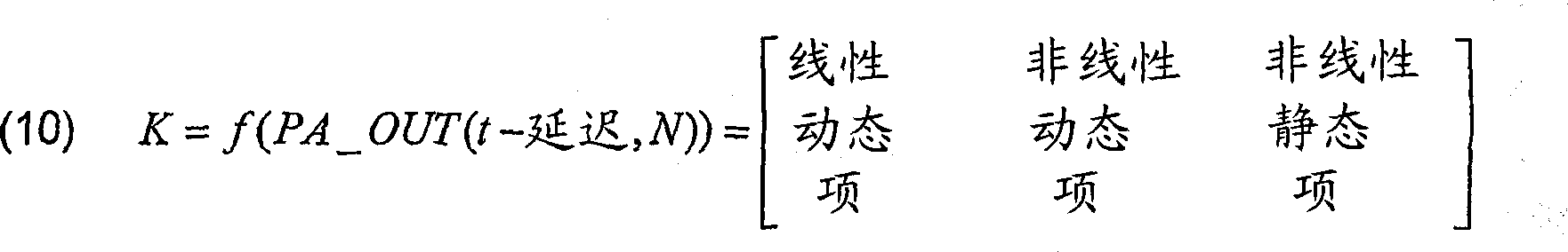
如果这个条件成立,数据被验证为良好的,然后它被呈现给数据同步器处理块604,该处理块使用部分(fractional)延时插入技术来对该输入和输出数据进行时间对准,以便补偿放大器和处理延时。适当的时间同步是对于保证DPD中记忆效应补偿的精确性的重要要求。时间对准的输入(PA_IN(t-延迟,N))和输出(PA_OUT(t-延迟,N))数据缓冲然后由预失真模型构建器处理块606进行处理,该处理块使用同步数据来计算核矩阵K,它以软件实施图3所示的DPD结构:If this condition holds, the data is verified as good, and then it is presented to the data
参数计算器处理块608然后使用核矩阵和经同步的输入数据PA_IN(t-延迟,N)来计算预失真器的参数。参数计算器处理块608优选地使用快速收敛最小平方处理来找出一个最佳参数值组,使得放大器的输出失真的二次范数平方(平均功率)最小化。DPD参数在参数平均处理块608中被低通滤波,以减小在DPD参数的计算中噪声和扰动的影响。最后,预失真模型证实器处理块612检验由参数计算器608计算的和由参数平均器610平均的参数值的一致性和有效性。在模型证实器612中实施的一个模型证实准则是:测试DPD参数的幅度是否处在预置的限度内。如果这个条件成立,则参数值被认为是有效的,以及它们作为更新的预失真系数被提供到DPD(108或202)。预失真模型证实器块614还保持以前计算的预失真系数的表,它可被使用于最新计算的参数估值是无效的或不提供可接受的预失真性能的情形。The parameter
参照图7,图上以示意图显示可被使用于以上相对于图3描述的动态补偿电路310和314的FIR滤波器的优选实施例。图7所示的相同的基本结构可被利用于具有在具体的电路之间变化的滤波器系数的每个电路。另外,在图3的各个电路的实施方案中,滤波器的级数N可以变化。如图所示,FIR滤波器在输入端700处接收数字输入,它将相应于用于线性动态补偿电路310的复数输入样本和相应于电路314中的输入包络样本。在700处的数字输入信号被提供到其数目等于想要的滤波器尺寸的一系列延迟级702。每个延迟级702的输出具有被馈送到乘法器704的抽头,该乘法器还接收被存储在非易失性存储器706的复数参数(或滤波器系数)。这些各个滤波器系数在以前描述的自适应实施例中由DPD控制器沿线路708被更新。N个乘法器704的输出被馈送到复数加法电路710,该复数加法电路提供在线路712上的复数滤波器输出。Referring to FIG. 7 , there is shown schematically a preferred embodiment of an FIR filter that may be used in the
参照图8,图上以示意图显示可被使用于图3的非线性静态补偿电路312的多项式生成器电路的优选实施例。如图所示,多项式生成器电路具有输入端800,该输入端接收数字包络信号(如以上相对于图3描述的),该包络信号被馈送到第一乘法器电路802,该乘法器电路还接收来自非易失性存储装置804的复数多项式系数。被存储在非易失性存储装置804中的多项式系数可以在以前描述的自适应实施例中由DPD控制器沿线路805更新。乘法器802的输出沿线路806被提供到复数加法电路810。多项式生成器电路的第二分支包括乘法器812和814以及非易失性存储装置816,该存储装置存储第二复数多项式系数。同样地,这个复数多项式系数可以由DPD控制器被更新,如由线路817表示的。乘法器814的输出被提供到加法电路810。多项式生成器的第三分支经由乘法器818被提供。多项式生成器电路的附加分支以图8所示的方式被级联,直至包括在非易失性存储装置828和乘法器824与826中的最后多项式系数的最后分支提供最后的N阶复数多项式值到加法电路810为止。加法电路810的输出在线路820上被提供,它总的相应于以上公式(2)的多项式。Referring to FIG. 8, a preferred embodiment of a polynomial generator circuit that may be used in the nonlinear
参照图9,图上以示意图显示可被使用于图3的每个电路336,338和340(以及任何附加的更高阶IIR电路310和314,如果方便的话)的IIR滤波器的优选实施例。所显示的电路相应于在滤波器转移函数中提供零点和极点的IIR滤波器,因此总的相应于上述的公式(4)-(6)的实现。在替换实施例中,全极点实施方案可被利用于与线路912上的信号对应的输入。在900处的数字输入信号被提供到一系列延迟级902,其数目等于在各个公式(4)-(6)的分子中实施的滤波器级的想要的数目。每个延迟级902的输出具有被馈送到乘法器904的抽头,该乘法器还接收被存储在非易失性存储器906的复数参数(或滤波器系数)。这些各个滤波器系数在以前描述的自适应实施例中由DPD控制器沿线路908更新。N个乘法器904的输出被馈送到复数加法电路910,该复数加法电路在线路912上提供复数输出。在线路912上的输出用作为加到滤波器的全极点部分的输入。在线路912上的信号被提供到第二系列延迟级914,其数目等于在各个公式(4)-(6)的分母中实施的滤波器级的想要的数目。每个延迟级914的输出具有被馈送到乘法器916的抽头,该乘法器还接收被存储在非易失性存储器918的复数参数(或滤波器系数)。这些各个滤波器系数在以前描述的自适应实施例中由DPD控制器沿线路920被更新。N个乘法器916的输出被馈送到复数加法电路922,该复数加法电路提供复数输出到加法电路910,该加法电路经由线路912提供线路924上的、来自滤波器的输出。在滤波器的上面部分和下面部分的级数,虽然由整数N表示,但一般可以是不同的。Referring to FIG. 9, there is shown schematically a preferred embodiment of an IIR filter that may be used in each of the
虽然本发明是相对于当前的优选实施例描述的,然而,本领域技术人员将会看到的,可以作出太多难以描述的、各种各样的修改,而仍保持在本发明的范围内。因此,以上详细说明的本质应当被看作为仅仅是说明性的而不是限制性的。While the invention has been described with respect to presently preferred embodiments, however, those skilled in the art will appreciate that a wide variety of modifications, too numerous to describe, can be made while remaining within the scope of the invention . Accordingly, the foregoing detailed description should be considered as illustrative in nature only and not restrictive.
Claims (21)
Applications Claiming Priority (5)
| Application Number | Priority Date | Filing Date | Title |
|---|---|---|---|
| US54978904P | 2004-03-03 | 2004-03-03 | |
| US60/549,789 | 2004-03-03 | ||
| US11/063,297 | 2005-02-22 | ||
| US11/063,297 US7336725B2 (en) | 2004-03-03 | 2005-02-22 | Digital predistortion system and method for high efficiency transmitters |
| PCT/US2005/005636 WO2005091865A2 (en) | 2004-03-03 | 2005-02-23 | Digital predistortion system and method for high efficiency trasmitters |
Publications (2)
| Publication Number | Publication Date |
|---|---|
| CN101156159A CN101156159A (en) | 2008-04-02 |
| CN101156159B true CN101156159B (en) | 2010-09-01 |
Family
ID=34914926
Family Applications (1)
| Application Number | Title | Priority Date | Filing Date |
|---|---|---|---|
| CN2005800066277A Expired - Fee Related CN101156159B (en) | 2004-03-03 | 2005-02-23 | Digital predistortion system and method for high efficiency transmitter |
Country Status (6)
| Country | Link |
|---|---|
| US (1) | US7336725B2 (en) |
| EP (2) | EP1749359B1 (en) |
| KR (1) | KR100802353B1 (en) |
| CN (1) | CN101156159B (en) |
| CA (1) | CA2557334C (en) |
| WO (1) | WO2005091865A2 (en) |
Families Citing this family (109)
| Publication number | Priority date | Publication date | Assignee | Title |
|---|---|---|---|---|
| US8380143B2 (en) | 2002-05-01 | 2013-02-19 | Dali Systems Co. Ltd | Power amplifier time-delay invariant predistortion methods and apparatus |
| US8811917B2 (en) | 2002-05-01 | 2014-08-19 | Dali Systems Co. Ltd. | Digital hybrid mode power amplifier system |
| US7991071B2 (en) | 2002-05-16 | 2011-08-02 | Rf Micro Devices, Inc. | AM to PM correction system for polar modulator |
| US7801244B2 (en) * | 2002-05-16 | 2010-09-21 | Rf Micro Devices, Inc. | Am to AM correction system for polar modulator |
| US7551686B1 (en) | 2004-06-23 | 2009-06-23 | Rf Micro Devices, Inc. | Multiple polynomial digital predistortion |
| US7529523B1 (en) | 2004-08-23 | 2009-05-05 | Rf Micro Devices, Inc. | N-th order curve fit for power calibration in a mobile terminal |
| DE102005013880B3 (en) * | 2005-03-24 | 2006-04-20 | Infineon Technologies Ag | Signals predistortion method, involves selecting table from set of two tables based on determined operating condition, and selecting pre distortion coefficient from selected table based on performance word and component |
| US7288988B2 (en) * | 2005-04-13 | 2007-10-30 | Powerwave Technologies, Inc. | Adaptive predistortion linearized amplifier system employing selective sampling |
| US8224265B1 (en) * | 2005-06-13 | 2012-07-17 | Rf Micro Devices, Inc. | Method for optimizing AM/AM and AM/PM predistortion in a mobile terminal |
| US7831221B2 (en) * | 2005-12-13 | 2010-11-09 | Andrew Llc | Predistortion system and amplifier for addressing group delay modulation |
| US7877060B1 (en) | 2006-02-06 | 2011-01-25 | Rf Micro Devices, Inc. | Fast calibration of AM/PM pre-distortion |
| US7962108B1 (en) | 2006-03-29 | 2011-06-14 | Rf Micro Devices, Inc. | Adaptive AM/PM compensation |
| US20070249290A1 (en) * | 2006-04-24 | 2007-10-25 | Sony Ericsson Mobile Communications Ab | Adaptive pre-distortion |
| DE102006031053A1 (en) * | 2006-07-05 | 2008-01-10 | Rohde & Schwarz Gmbh & Co. Kg | Arrangement for determining the operating characteristics of a high-frequency power amplifier |
| DE102006031046A1 (en) * | 2006-07-05 | 2008-01-10 | Rohde & Schwarz Gmbh & Co. Kg | Arrangement for determining the operating characteristics of a high-frequency power amplifier |
| US7689182B1 (en) | 2006-10-12 | 2010-03-30 | Rf Micro Devices, Inc. | Temperature compensated bias for AM/PM improvement |
| US8078561B2 (en) * | 2006-12-01 | 2011-12-13 | Uti Limited Partnership | Nonlinear behavior models and methods for use thereof in wireless radio systems |
| CN102017553B (en) | 2006-12-26 | 2014-10-15 | 大力系统有限公司 | Method and system for baseband predistortion linearization in a multi-channel broadband communication system |
| US8395256B2 (en) * | 2007-02-02 | 2013-03-12 | Harris Stratex Networks Operating Corporation | Packaging for low-cost, high-performance microwave and millimeter wave modules |
| US8275071B2 (en) | 2007-05-17 | 2012-09-25 | Harris Stratex Networks Operating Corporation | Compact dual receiver architecture for point to point radio |
| US7782765B2 (en) | 2007-01-22 | 2010-08-24 | Harris Stratex Networks Operating Corporation | Distributed protection switching architecture for point-to-point microwave radio systems |
| US8095088B2 (en) | 2007-05-17 | 2012-01-10 | Harris Stratex Networks Operating Corporation | Compact wide dynamic range transmitter for point to point radio |
| US8019015B2 (en) * | 2007-02-26 | 2011-09-13 | Harris Corporation | Linearization of RF power amplifiers using an adaptive subband predistorter |
| US8009762B1 (en) | 2007-04-17 | 2011-08-30 | Rf Micro Devices, Inc. | Method for calibrating a phase distortion compensated polar modulated radio frequency transmitter |
| FR2915642B1 (en) * | 2007-04-25 | 2009-07-10 | Eads Secure Networks Soc Par A | LINEARIZATION IN A TRANSMISSION CHAIN |
| US7541868B2 (en) * | 2007-05-31 | 2009-06-02 | Andrew, Llc | Delay modulator pre-distortion circuit for an amplifier |
| US7899416B2 (en) * | 2007-11-14 | 2011-03-01 | Crestcom, Inc. | RF transmitter with heat compensation and method therefor |
| KR101669173B1 (en) * | 2007-12-07 | 2016-10-25 | 달리 시스템즈 씨오. 엘티디. | Baseband-derived wideband rf digital predistortion system |
| CN100578922C (en) * | 2007-12-17 | 2010-01-06 | 华为技术有限公司 | High efficiency power amplifier |
| EP2248316B1 (en) * | 2008-01-24 | 2012-07-18 | Agence Spatiale Européenne | A method for compensating signal distortion in an emitting payload |
| US8064851B2 (en) * | 2008-03-06 | 2011-11-22 | Crestcom, Inc. | RF transmitter with bias-signal-induced distortion compensation and method therefor |
| CN101247153B (en) * | 2008-03-13 | 2011-11-30 | 中兴通讯股份有限公司 | Method for improving power amplifier efficiency and digital predistortion broadband communicator |
| US8066433B2 (en) | 2008-03-14 | 2011-11-29 | Pro-Mart Industries, Inc. | Valve for vacuum storage bag |
| US7642850B2 (en) * | 2008-04-02 | 2010-01-05 | Harris Corporation | Feedforward linearization of RF power amplifiers |
| US20090323856A1 (en) * | 2008-06-27 | 2009-12-31 | Crestcom, Inc. | Transmit-canceling transceiver responsive to heat signal and method therefor |
| GB2465399B (en) | 2008-11-17 | 2015-07-15 | Nujira Ltd | Generation of pre-distortion coefficients |
| US8160191B2 (en) * | 2008-12-01 | 2012-04-17 | Rockstar Bidco Lp | Correction of quadrature errors |
| US20100323641A1 (en) * | 2009-06-22 | 2010-12-23 | Qualcomm Incorporated | Method and apparatus for using pre-distortion and feedback to mitigate nonlinearity of circuits |
| DE102010038482B4 (en) * | 2009-07-31 | 2014-07-24 | Intel Mobile Communications GmbH | Digital predistortion and compensation of an operating condition effect |
| US8489042B1 (en) | 2009-10-08 | 2013-07-16 | Rf Micro Devices, Inc. | Polar feedback linearization |
| JP5299298B2 (en) * | 2010-01-29 | 2013-09-25 | 富士通株式会社 | Distortion compensation device, transmission device, and distortion compensation method |
| US20120233210A1 (en) * | 2011-03-12 | 2012-09-13 | Matthew Thomas Bogosian | Storage of Arbitrary Points in N-Space and Retrieval of Subset thereof Based on Criteria Including Maximum Distance to an Arbitrary Reference Point |
| KR101102465B1 (en) | 2010-05-03 | 2012-01-05 | 한국과학기술원 | Digital Predistortion Apparatus and Method for Broadband Power Amplifier |
| US8682338B2 (en) | 2010-09-14 | 2014-03-25 | Dali Systems Co., Ltd. | Remotely reconfigurable distributed antenna system and methods |
| US8635044B2 (en) * | 2011-04-27 | 2014-01-21 | Advanced Micro Devices, Inc. | Transient thermal modeling of multisource power devices |
| GB2490749A (en) * | 2011-05-12 | 2012-11-14 | Nokia Siemens Networks Oy | Linearization of an RF power amplifier using a combined FIR-IIR amplifier model |
| JP5673475B2 (en) * | 2011-09-30 | 2015-02-18 | 富士通株式会社 | Distortion compensation apparatus and distortion compensation method |
| TW201328172A (en) * | 2011-11-17 | 2013-07-01 | Analog Devices Inc | System linearization |
| CN102725977B (en) * | 2011-12-01 | 2014-07-09 | 华为技术有限公司 | A kind of optical signal compensation device |
| US8798559B2 (en) * | 2012-02-28 | 2014-08-05 | Telefonaktiebolaget L M Ericsson (Publ) | FIR/IIR filter predistorter for power amplifiers exhibiting short-term and/or long-term memory effects |
| CN103974395B (en) * | 2013-01-29 | 2018-04-10 | 中兴通讯股份有限公司 | The power regulating method and device of power detection before a kind of digital pre-distortion based on low delay |
| US8995571B2 (en) * | 2013-03-14 | 2015-03-31 | Analog Devices Global | Baseband digital pre-distortion architecture |
| US9214969B2 (en) | 2013-05-09 | 2015-12-15 | King Fahd University Of Petroleum And Minerals | Scalable digital predistortion system |
| US9595982B2 (en) | 2013-05-20 | 2017-03-14 | Analog Devices, Inc. | Relaxed digitization system linearization |
| JP6123497B2 (en) * | 2013-06-03 | 2017-05-10 | 住友電気工業株式会社 | Distortion compensation device and wireless communication device |
| GB2519361B (en) * | 2013-10-21 | 2015-09-16 | Nujira Ltd | Reduced bandwidth of signal in an envelope path for envelope tracking system |
| US9337781B2 (en) | 2013-12-09 | 2016-05-10 | King Fahd University Of Petroleum And Minerals | Augmented twin nonlinear two-box modeling and predistortion method for power amplifiers and transmitters |
| CN103715992B (en) * | 2013-12-17 | 2016-08-17 | 东南大学 | Based on the power amplifier predistortion device and method simplifying Volterra progression |
| US9160280B1 (en) * | 2014-05-21 | 2015-10-13 | King Fahd University Of Petroleum And Minerals | Memory polynomial based digital predistorter |
| ES2667678T3 (en) | 2014-07-04 | 2018-05-14 | Ses S.A. | Procedures, devices and software to compensate for nonlinearities of a communication channel |
| CN105445682B (en) * | 2014-07-25 | 2018-08-21 | 通用电气公司 | MR imaging apparatus, radio frequency amplification system and method |
| FR3036901B1 (en) * | 2014-07-29 | 2020-10-30 | Thales Sa | PREDISTORSION DEVICE AND ASSOCIATED PREDISTORSION CALCULATION PROCESS |
| US9461597B2 (en) | 2014-11-05 | 2016-10-04 | King Fahd University Of Petroleum And Minerals | Weighted memory polynomial method and system for power amplifiers predistortion |
| CN107078702B (en) * | 2014-11-19 | 2019-11-29 | 华为技术有限公司 | A kind of device and method of pre-distortion |
| WO2016154933A1 (en) * | 2015-03-31 | 2016-10-06 | 华为技术有限公司 | Digital pre-distortion correcting method and device |
| US10122391B2 (en) * | 2015-09-30 | 2018-11-06 | Apple Inc. | Radio frequency systems and methods for polar phase distortion calibration |
| US9634695B1 (en) * | 2015-10-29 | 2017-04-25 | Apple Inc. | Wireless devices having multiple transmit chains with predistortion circuitry |
| US9590668B1 (en) * | 2015-11-30 | 2017-03-07 | NanoSemi Technologies | Digital compensator |
| EP3252949B1 (en) * | 2016-06-01 | 2020-03-18 | Intel IP Corporation | Methods and devices for predistortion of signals |
| US9787336B1 (en) * | 2016-09-29 | 2017-10-10 | Intel IP Corporation | Device and method of pre-distortion of power amplifier input signals |
| US9866269B1 (en) * | 2016-11-17 | 2018-01-09 | Xilinx, Inc. | Method of and circuit for predistortion for a power amplifier |
| RU2652435C1 (en) * | 2017-04-12 | 2018-04-26 | Федеральное государственное казенное военное образовательное учреждение высшего образования "Военная академия воздушно-космической обороны имени Маршала Советского Союза Г.К. Жукова" Министерства обороны Российской Федерации | Method of determination of optimal part of frequency band affected by intentional interference in communication systems with broadband signals |
| US10732714B2 (en) | 2017-05-08 | 2020-08-04 | Cirrus Logic, Inc. | Integrated haptic system |
| JP7024420B2 (en) * | 2018-01-12 | 2022-02-24 | 日本電気株式会社 | Strain compensation device and strain compensation method |
| US10832537B2 (en) | 2018-04-04 | 2020-11-10 | Cirrus Logic, Inc. | Methods and apparatus for outputting a haptic signal to a haptic transducer |
| FR3080723B1 (en) | 2018-04-25 | 2021-08-06 | Wupatec | BASIC BAND LINEARIZATION SYSTEM AND METHOD FOR A CLASS G RADIOFREQUENCY POWER AMPLIFIER |
| US10432240B1 (en) * | 2018-05-22 | 2019-10-01 | Micron Technology, Inc. | Wireless devices and systems including examples of compensating power amplifier noise |
| US11269415B2 (en) | 2018-08-14 | 2022-03-08 | Cirrus Logic, Inc. | Haptic output systems |
| US11791776B2 (en) * | 2018-08-29 | 2023-10-17 | Sumitomo Electric Industries, Ltd. | Distortion compensation device, wireless communicator, predistorter, distortion compensation method, and computer program |
| GB201817495D0 (en) | 2018-10-26 | 2018-12-12 | Cirrus Logic Int Semiconductor Ltd | A force sensing system and method |
| US11509292B2 (en) | 2019-03-29 | 2022-11-22 | Cirrus Logic, Inc. | Identifying mechanical impedance of an electromagnetic load using least-mean-squares filter |
| US12035445B2 (en) | 2019-03-29 | 2024-07-09 | Cirrus Logic Inc. | Resonant tracking of an electromagnetic load |
| US10828672B2 (en) | 2019-03-29 | 2020-11-10 | Cirrus Logic, Inc. | Driver circuitry |
| US11283337B2 (en) * | 2019-03-29 | 2022-03-22 | Cirrus Logic, Inc. | Methods and systems for improving transducer dynamics |
| US11644370B2 (en) | 2019-03-29 | 2023-05-09 | Cirrus Logic, Inc. | Force sensing with an electromagnetic load |
| US10955955B2 (en) | 2019-03-29 | 2021-03-23 | Cirrus Logic, Inc. | Controller for use in a device comprising force sensors |
| CN110289869B (en) * | 2019-05-25 | 2021-01-01 | 西南电子技术研究所(中国电子科技集团公司第十研究所) | Digital predistortion model of ultrashort wave power amplifier |
| US10976825B2 (en) | 2019-06-07 | 2021-04-13 | Cirrus Logic, Inc. | Methods and apparatuses for controlling operation of a vibrational output system and/or operation of an input sensor system |
| CN110276122B (en) * | 2019-06-19 | 2023-01-06 | 复旦大学 | Digital predistortion front-end circuit suitable for multi-bit digital quadrature transmitter |
| WO2020254788A1 (en) | 2019-06-21 | 2020-12-24 | Cirrus Logic International Semiconductor Limited | A method and apparatus for configuring a plurality of virtual buttons on a device |
| US10693509B1 (en) * | 2019-10-02 | 2020-06-23 | Analog Devices International Unlimited Company | Digital predistortion with power-specific capture selection |
| US11408787B2 (en) | 2019-10-15 | 2022-08-09 | Cirrus Logic, Inc. | Control methods for a force sensor system |
| US11380175B2 (en) | 2019-10-24 | 2022-07-05 | Cirrus Logic, Inc. | Reproducibility of haptic waveform |
| GB2588959B (en) * | 2019-11-15 | 2022-03-23 | Cisco Tech Inc | Method and apparatus for pre-distorting an input signal for an optical transmitter |
| US12276687B2 (en) | 2019-12-05 | 2025-04-15 | Cirrus Logic Inc. | Methods and systems for estimating coil impedance of an electromagnetic transducer |
| CN112994809B (en) * | 2019-12-12 | 2023-04-14 | 珠海全志科技股份有限公司 | Digital predistortion performance detection method, device, computer equipment and storage medium |
| CN111181499A (en) * | 2020-01-17 | 2020-05-19 | 南通大学 | Digital predistortion adaptive processing method and system for sea area access equipment |
| JP7393741B2 (en) * | 2020-03-30 | 2023-12-07 | 住友電気工業株式会社 | Distortion compensation device, distortion compensation method, computer program, and communication device |
| US11662821B2 (en) | 2020-04-16 | 2023-05-30 | Cirrus Logic, Inc. | In-situ monitoring, calibration, and testing of a haptic actuator |
| US12244253B2 (en) | 2020-04-16 | 2025-03-04 | Cirrus Logic Inc. | Restricting undesired movement of a haptic actuator |
| CN111510406B (en) * | 2020-06-03 | 2024-05-17 | 上海创远仪器技术股份有限公司 | Circuit and method for implementing real-time predistortion calibration of broadband IQ modulation |
| US11251819B1 (en) * | 2020-12-23 | 2022-02-15 | Xilinx, Inc. | Thermal effect mitigation for digital pre-distortion |
| EP4278482B1 (en) * | 2021-03-01 | 2025-01-01 | Huawei Technologies Co., Ltd. | Method and apparatus for predistortion of a digital signal in a transmitter chain |
| TN2023000034A1 (en) * | 2021-03-16 | 2024-10-01 | Fadhel Ghannouchi | Apparatus and method for artificial intelligence driven digital predistortion in transmission systems having multiple impairments |
| US11933822B2 (en) | 2021-06-16 | 2024-03-19 | Cirrus Logic Inc. | Methods and systems for in-system estimation of actuator parameters |
| US11765499B2 (en) | 2021-06-22 | 2023-09-19 | Cirrus Logic Inc. | Methods and systems for managing mixed mode electromechanical actuator drive |
| US11908310B2 (en) | 2021-06-22 | 2024-02-20 | Cirrus Logic Inc. | Methods and systems for detecting and managing unexpected spectral content in an amplifier system |
| CN114189413B (en) * | 2021-11-30 | 2023-12-29 | 中国电子科技集团公司第五十四研究所 | Multi-carrier broadband digital predistortion device based on FPGA |
| CN118659748B (en) * | 2024-08-20 | 2024-11-12 | 成都安普利电子有限责任公司 | A dynamic management system for microwave power amplifiers |
Citations (3)
| Publication number | Priority date | Publication date | Assignee | Title |
|---|---|---|---|---|
| US5867065A (en) * | 1997-05-07 | 1999-02-02 | Glenayre Electronics, Inc. | Frequency selective predistortion in a linear transmitter |
| US6141390A (en) * | 1997-05-05 | 2000-10-31 | Glenayre Electronics, Inc. | Predistortion in a linear transmitter using orthogonal kernels |
| US6570444B2 (en) * | 2000-01-26 | 2003-05-27 | Pmc-Sierra, Inc. | Low noise wideband digital predistortion amplifier |
Family Cites Families (46)
| Publication number | Priority date | Publication date | Assignee | Title |
|---|---|---|---|---|
| US5049832A (en) * | 1990-04-20 | 1991-09-17 | Simon Fraser University | Amplifier linearization by adaptive predistortion |
| JP3156439B2 (en) * | 1993-04-20 | 2001-04-16 | 三菱電機株式会社 | Distortion compensation circuit |
| US5732333A (en) * | 1996-02-14 | 1998-03-24 | Glenayre Electronics, Inc. | Linear transmitter using predistortion |
| US5892397A (en) * | 1996-03-29 | 1999-04-06 | Spectrian | Adaptive compensation of RF amplifier distortion by injecting predistortion signal derived from respectively different functions of input signal amplitude |
| US5760646A (en) * | 1996-03-29 | 1998-06-02 | Spectrian | Feed-forward correction loop with adaptive predistortion injection for linearization of RF power amplifier |
| US6282247B1 (en) * | 1997-09-12 | 2001-08-28 | Ericsson Inc. | Method and apparatus for digital compensation of radio distortion over a wide range of temperatures |
| US6498858B2 (en) * | 1997-11-18 | 2002-12-24 | Gn Resound A/S | Feedback cancellation improvements |
| US6075411A (en) * | 1997-12-22 | 2000-06-13 | Telefonaktiebolaget Lm Ericsson | Method and apparatus for wideband predistortion linearization |
| US5959500A (en) * | 1998-01-26 | 1999-09-28 | Glenayre Electronics, Inc. | Model-based adaptive feedforward amplifier linearizer |
| GB9804835D0 (en) * | 1998-03-06 | 1998-04-29 | Wireless Systems Int Ltd | Predistorter |
| US6519010B2 (en) * | 1998-06-26 | 2003-02-11 | Harris Corporation | Broadcast transmission system with sampling and correction arrangement for correcting distortion caused by amplifying and signal conditioning components |
| US6236837B1 (en) * | 1998-07-30 | 2001-05-22 | Motorola, Inc. | Polynomial Predistortion linearizing device, method, phone and base station |
| KR100326176B1 (en) * | 1998-08-06 | 2002-04-17 | 윤종용 | Apparatus and method for linearizing power amplification using predistortion and feedfoward method in rf communicaiton |
| GB2348755B (en) * | 1999-04-01 | 2001-03-07 | Wireless Systems Int Ltd | Signal processing |
| US6118335A (en) * | 1999-05-06 | 2000-09-12 | Nortel Networks Corporation | Method and apparatus for providing adaptive predistortion in power amplifier and base station utilizing same |
| CN1249913C (en) * | 1999-05-28 | 2006-04-05 | 富士通株式会社 | Predistortion type distortion compensatino amplifier |
| US6342810B1 (en) * | 1999-07-13 | 2002-01-29 | Pmc-Sierra, Inc. | Predistortion amplifier system with separately controllable amplifiers |
| US6356146B1 (en) * | 1999-07-13 | 2002-03-12 | Pmc-Sierra, Inc. | Amplifier measurement and modeling processes for use in generating predistortion parameters |
| US6587514B1 (en) * | 1999-07-13 | 2003-07-01 | Pmc-Sierra, Inc. | Digital predistortion methods for wideband amplifiers |
| EP1204216B1 (en) * | 1999-07-28 | 2011-04-20 | Fujitsu Limited | Method and apparatus for distortion compensation of radio device |
| EP1199814B1 (en) * | 1999-07-28 | 2006-09-13 | Fujitsu Limited | Radio device with distortion compensation |
| JP4183364B2 (en) * | 1999-12-28 | 2008-11-19 | 富士通株式会社 | Distortion compensation device |
| JP2001352219A (en) * | 2000-06-08 | 2001-12-21 | Sony Corp | Nonlinear distortion compensator |
| US6304140B1 (en) * | 2000-06-12 | 2001-10-16 | Motorola, Inc. | Digital predistortion for amplifiers |
| CN1166138C (en) * | 2000-07-20 | 2004-09-08 | 华为技术有限公司 | Adaptive digital pre-distortion method and device for wideband transmitter |
| US6751043B2 (en) * | 2000-12-15 | 2004-06-15 | Texas Instruments Incorporated | Digital servo control system for a hard disc drive using a voice coil motor in voltage mode |
| JP2002223130A (en) * | 2001-01-25 | 2002-08-09 | Fujitsu Ltd | Transmission device and transmission method |
| WO2002061938A1 (en) * | 2001-01-31 | 2002-08-08 | Fujitsu Limited | Distortion compensation apparatus |
| US6593812B2 (en) * | 2001-04-23 | 2003-07-15 | Telefonaktiebolaget Lm Ericsson | Automatic optimization of linearity for envelope feedback RF amplifier linearization |
| US20020171485A1 (en) * | 2001-05-18 | 2002-11-21 | Spectrian Corporation | Digitally implemented predistorter control mechanism for linearizing high efficiency RF power amplifiers |
| US6683495B2 (en) * | 2001-06-28 | 2004-01-27 | Simon Fraser University | Reduced architecture for multibranch feedforward power amplifier linearizers |
| US7015751B2 (en) * | 2001-06-28 | 2006-03-21 | Simon Fraser University | Decorrelated power amplifier linearizers |
| US6570514B1 (en) * | 2001-12-21 | 2003-05-27 | Scott R. Velazquez | Linearity error compensator |
| US6731168B2 (en) * | 2002-02-06 | 2004-05-04 | Intersil Americas, Inc. | Power amplifier linearizer that compensates for long-time-constant memory effects and method therefor |
| US6680648B2 (en) * | 2002-03-08 | 2004-01-20 | The Aerospace Corporation | High power amplifier predistorter system |
| JP3874688B2 (en) * | 2002-03-29 | 2007-01-31 | 富士通株式会社 | Distortion compensation device |
| US6794939B2 (en) * | 2002-05-31 | 2004-09-21 | Lucent Technologies Inc. | Signal predistortion using a combination of multiple predistortion techniques |
| US6642786B1 (en) * | 2002-08-15 | 2003-11-04 | Electronics And Telecommunications Research Institute | Piecewise polynomial predistortion method and apparatus for compensating nonlinear distortion of high power amplifier |
| US6882251B2 (en) * | 2002-12-09 | 2005-04-19 | Com Dev Ltd. | Microwave filter with adaptive predistortion |
| US7170342B2 (en) * | 2002-12-10 | 2007-01-30 | Ntt Docomo, Inc. | Linear power amplification method and linear power amplifier |
| US6765440B2 (en) * | 2002-12-18 | 2004-07-20 | Andrew Corporation | Model-based feed-forward linearization of amplifiers |
| US6812792B2 (en) * | 2003-01-02 | 2004-11-02 | Harris Corporation | Precorrection of a nonlinear amplifier |
| US7403573B2 (en) * | 2003-01-15 | 2008-07-22 | Andrew Corporation | Uncorrelated adaptive predistorter |
| KR20040071556A (en) * | 2003-02-06 | 2004-08-12 | 삼성전자주식회사 | Polynomial predistorter using complex vector multiplication and method thereof |
| JP4033794B2 (en) * | 2003-03-24 | 2008-01-16 | 株式会社エヌ・ティ・ティ・ドコモ | High efficiency linear power amplifier |
| US6781537B1 (en) * | 2003-06-10 | 2004-08-24 | Nortel Networks Limited | High speed digital to analog converter |
-
2005
- 2005-02-22 US US11/063,297 patent/US7336725B2/en active Active
- 2005-02-23 CA CA2557334A patent/CA2557334C/en not_active Expired - Fee Related
- 2005-02-23 WO PCT/US2005/005636 patent/WO2005091865A2/en not_active Ceased
- 2005-02-23 EP EP05713947A patent/EP1749359B1/en not_active Expired - Lifetime
- 2005-02-23 EP EP12178650A patent/EP2521260A1/en not_active Withdrawn
- 2005-02-23 KR KR1020067020665A patent/KR100802353B1/en not_active Expired - Fee Related
- 2005-02-23 CN CN2005800066277A patent/CN101156159B/en not_active Expired - Fee Related
Patent Citations (3)
| Publication number | Priority date | Publication date | Assignee | Title |
|---|---|---|---|---|
| US6141390A (en) * | 1997-05-05 | 2000-10-31 | Glenayre Electronics, Inc. | Predistortion in a linear transmitter using orthogonal kernels |
| US5867065A (en) * | 1997-05-07 | 1999-02-02 | Glenayre Electronics, Inc. | Frequency selective predistortion in a linear transmitter |
| US6570444B2 (en) * | 2000-01-26 | 2003-05-27 | Pmc-Sierra, Inc. | Low noise wideband digital predistortion amplifier |
Also Published As
| Publication number | Publication date |
|---|---|
| CN101156159A (en) | 2008-04-02 |
| EP1749359A4 (en) | 2010-05-19 |
| CA2557334C (en) | 2013-01-08 |
| WO2005091865A2 (en) | 2005-10-06 |
| CA2557334A1 (en) | 2005-10-06 |
| US7336725B2 (en) | 2008-02-26 |
| EP1749359B1 (en) | 2012-09-26 |
| WO2005091865A3 (en) | 2007-06-14 |
| EP1749359A2 (en) | 2007-02-07 |
| EP2521260A1 (en) | 2012-11-07 |
| KR100802353B1 (en) | 2008-02-13 |
| KR20060116252A (en) | 2006-11-14 |
| US20050195919A1 (en) | 2005-09-08 |
Similar Documents
| Publication | Publication Date | Title |
|---|---|---|
| CN101156159B (en) | Digital predistortion system and method for high efficiency transmitter | |
| CN101040502B (en) | Wideband enhanced digital injection predistortion system and method | |
| CN101911477B (en) | Predistorter | |
| JP5761646B2 (en) | System and method for modulation agnostic digital hybrid mode power amplifier | |
| US7333559B2 (en) | Digital predistorter for a wideband power amplifier and adaptation method | |
| US6072364A (en) | Adaptive digital predistortion for power amplifiers with real time modeling of memoryless complex gains | |
| KR100959032B1 (en) | Frequency-dependent magnitude predistortion to reduce spurious emissions in communication networks | |
| KR101440121B1 (en) | Distortion compensation apparatus, signal transmitter and method for transmitting signal | |
| KR101058733B1 (en) | Precompensation Device Compensates for Nonlinear Distortion Characteristics of Power Amplifiers | |
| US6956433B2 (en) | Polynomial predistorter using complex vector multiplication | |
| US7251293B2 (en) | Digital pre-distortion for the linearization of power amplifiers with asymmetrical characteristics | |
| US20020171485A1 (en) | Digitally implemented predistorter control mechanism for linearizing high efficiency RF power amplifiers | |
| HK1205382A1 (en) | Method and system for baseband predistortion linearization in multi-channel wideband communication systems | |
| JP2011234322A (en) | Memory effect canceller of power amplifier, and radio transmitter | |
| EP2837093B1 (en) | Digital predistorter (dpd) structure based on dynamic deviation reduction (ddr)-based volterra series | |
| KR20050064485A (en) | Predistortion apparatus and method for compensating non-linearility of the power amplifier | |
| KR100487209B1 (en) | Predistortion apparatus and method for compensating non-linearility of the power amplifier using look-up table | |
| KR101470817B1 (en) | Apparatus and method of predistortion of multiple nonlinear amplifiers with single feedback loop |
Legal Events
| Date | Code | Title | Description |
|---|---|---|---|
| C06 | Publication | ||
| PB01 | Publication | ||
| C10 | Entry into substantive examination | ||
| SE01 | Entry into force of request for substantive examination | ||
| C14 | Grant of patent or utility model | ||
| GR01 | Patent grant | ||
| ASS | Succession or assignment of patent right |
Owner name: POWERWAVE TECHNOLOGIES INC. Free format text: FORMER OWNER: P-WAVE HOLDING LLC Effective date: 20150520 Owner name: INTEL CORP . Free format text: FORMER OWNER: POWERWAVE TECHNOLOGIES INC. Effective date: 20150520 Owner name: P-WAVE HOLDING LLC Free format text: FORMER OWNER: POWERWAVE TCH INC. Effective date: 20150520 |
|
| C41 | Transfer of patent application or patent right or utility model | ||
| TR01 | Transfer of patent right |
Effective date of registration: 20150520 Address after: California, USA Patentee after: INTEL Corp. Address before: Luxemburg Luxemburg Patentee before: POWERWAVE TECHNOLOGIES, Inc. Effective date of registration: 20150520 Address after: Luxemburg Luxemburg Patentee after: POWERWAVE TECHNOLOGIES, Inc. Address before: California, USA Patentee before: P-wave holding LLC Effective date of registration: 20150520 Address after: California, USA Patentee after: P-wave holding LLC Address before: California, USA Patentee before: POWERWAVE TECHNOLOGIES, Inc. |
|
| CF01 | Termination of patent right due to non-payment of annual fee | ||
| CF01 | Termination of patent right due to non-payment of annual fee |
Granted publication date: 20100901 Termination date: 20200223 |