CN101099167B - Integrated EAS/RFID device and disabling device therefor - Google Patents
Integrated EAS/RFID device and disabling device therefor Download PDFInfo
- Publication number
- CN101099167B CN101099167B CN2005800460432A CN200580046043A CN101099167B CN 101099167 B CN101099167 B CN 101099167B CN 2005800460432 A CN2005800460432 A CN 2005800460432A CN 200580046043 A CN200580046043 A CN 200580046043A CN 101099167 B CN101099167 B CN 101099167B
- Authority
- CN
- China
- Prior art keywords
- switch
- semiconductor
- antenna
- eas
- rfid
- Prior art date
- Legal status (The legal status is an assumption and is not a legal conclusion. Google has not performed a legal analysis and makes no representation as to the accuracy of the status listed.)
- Expired - Fee Related
Links
Images


Classifications
-
- G—PHYSICS
- G06—COMPUTING OR CALCULATING; COUNTING
- G06K—GRAPHICAL DATA READING; PRESENTATION OF DATA; RECORD CARRIERS; HANDLING RECORD CARRIERS
- G06K19/00—Record carriers for use with machines and with at least a part designed to carry digital markings
- G06K19/06—Record carriers for use with machines and with at least a part designed to carry digital markings characterised by the kind of the digital marking, e.g. shape, nature, code
- G06K19/067—Record carriers with conductive marks, printed circuits or semiconductor circuit elements, e.g. credit or identity cards also with resonating or responding marks without active components
- G06K19/07—Record carriers with conductive marks, printed circuits or semiconductor circuit elements, e.g. credit or identity cards also with resonating or responding marks without active components with integrated circuit chips
-
- G—PHYSICS
- G08—SIGNALLING
- G08B—SIGNALLING OR CALLING SYSTEMS; ORDER TELEGRAPHS; ALARM SYSTEMS
- G08B13/00—Burglar, theft or intruder alarms
- G08B13/22—Electrical actuation
- G08B13/24—Electrical actuation by interference with electromagnetic field distribution
- G08B13/2402—Electronic Article Surveillance [EAS], i.e. systems using tags for detecting removal of a tagged item from a secure area, e.g. tags for detecting shoplifting
- G08B13/2405—Electronic Article Surveillance [EAS], i.e. systems using tags for detecting removal of a tagged item from a secure area, e.g. tags for detecting shoplifting characterised by the tag technology used
- G08B13/2414—Electronic Article Surveillance [EAS], i.e. systems using tags for detecting removal of a tagged item from a secure area, e.g. tags for detecting shoplifting characterised by the tag technology used using inductive tags
- G08B13/2417—Electronic Article Surveillance [EAS], i.e. systems using tags for detecting removal of a tagged item from a secure area, e.g. tags for detecting shoplifting characterised by the tag technology used using inductive tags having a radio frequency identification chip
-
- G—PHYSICS
- G06—COMPUTING OR CALCULATING; COUNTING
- G06K—GRAPHICAL DATA READING; PRESENTATION OF DATA; RECORD CARRIERS; HANDLING RECORD CARRIERS
- G06K19/00—Record carriers for use with machines and with at least a part designed to carry digital markings
-
- G—PHYSICS
- G06—COMPUTING OR CALCULATING; COUNTING
- G06K—GRAPHICAL DATA READING; PRESENTATION OF DATA; RECORD CARRIERS; HANDLING RECORD CARRIERS
- G06K19/00—Record carriers for use with machines and with at least a part designed to carry digital markings
- G06K19/06—Record carriers for use with machines and with at least a part designed to carry digital markings characterised by the kind of the digital marking, e.g. shape, nature, code
- G06K19/067—Record carriers with conductive marks, printed circuits or semiconductor circuit elements, e.g. credit or identity cards also with resonating or responding marks without active components
- G06K19/07—Record carriers with conductive marks, printed circuits or semiconductor circuit elements, e.g. credit or identity cards also with resonating or responding marks without active components with integrated circuit chips
- G06K19/0723—Record carriers with conductive marks, printed circuits or semiconductor circuit elements, e.g. credit or identity cards also with resonating or responding marks without active components with integrated circuit chips the record carrier comprising an arrangement for non-contact communication, e.g. wireless communication circuits on transponder cards, non-contact smart cards or RFIDs
-
- G—PHYSICS
- G06—COMPUTING OR CALCULATING; COUNTING
- G06K—GRAPHICAL DATA READING; PRESENTATION OF DATA; RECORD CARRIERS; HANDLING RECORD CARRIERS
- G06K19/00—Record carriers for use with machines and with at least a part designed to carry digital markings
- G06K19/06—Record carriers for use with machines and with at least a part designed to carry digital markings characterised by the kind of the digital marking, e.g. shape, nature, code
- G06K19/067—Record carriers with conductive marks, printed circuits or semiconductor circuit elements, e.g. credit or identity cards also with resonating or responding marks without active components
- G06K19/07—Record carriers with conductive marks, printed circuits or semiconductor circuit elements, e.g. credit or identity cards also with resonating or responding marks without active components with integrated circuit chips
- G06K19/077—Constructional details, e.g. mounting of circuits in the carrier
- G06K19/07749—Constructional details, e.g. mounting of circuits in the carrier the record carrier being capable of non-contact communication, e.g. constructional details of the antenna of a non-contact smart card
-
- G—PHYSICS
- G06—COMPUTING OR CALCULATING; COUNTING
- G06K—GRAPHICAL DATA READING; PRESENTATION OF DATA; RECORD CARRIERS; HANDLING RECORD CARRIERS
- G06K7/00—Methods or arrangements for sensing record carriers, e.g. for reading patterns
- G06K7/0008—General problems related to the reading of electronic memory record carriers, independent of its reading method, e.g. power transfer
-
- G—PHYSICS
- G08—SIGNALLING
- G08B—SIGNALLING OR CALLING SYSTEMS; ORDER TELEGRAPHS; ALARM SYSTEMS
- G08B13/00—Burglar, theft or intruder alarms
- G08B13/22—Electrical actuation
- G08B13/24—Electrical actuation by interference with electromagnetic field distribution
- G08B13/2402—Electronic Article Surveillance [EAS], i.e. systems using tags for detecting removal of a tagged item from a secure area, e.g. tags for detecting shoplifting
- G08B13/2428—Tag details
- G08B13/2448—Tag with at least dual detection means, e.g. combined inductive and ferromagnetic tags, dual frequencies within a single technology, tampering detection or signalling means on the tag
Landscapes
- Engineering & Computer Science (AREA)
- Physics & Mathematics (AREA)
- General Physics & Mathematics (AREA)
- Theoretical Computer Science (AREA)
- Computer Hardware Design (AREA)
- Microelectronics & Electronic Packaging (AREA)
- Electromagnetism (AREA)
- Computer Security & Cryptography (AREA)
- Automation & Control Theory (AREA)
- Computer Networks & Wireless Communication (AREA)
- Artificial Intelligence (AREA)
- Computer Vision & Pattern Recognition (AREA)
- Burglar Alarm Systems (AREA)
- Near-Field Transmission Systems (AREA)
- Semiconductor Integrated Circuits (AREA)
- Lock And Its Accessories (AREA)
Abstract
本发明提供了一种集成电子商品防盗(EAS)和射频识别(RFID)标记,其中,半导体设备可以与天线耦合,以便接收和向天线转发能量和信号。该半导体设备的电流接收前端部分与该设备的至少另一个部分通信,从而可以在接收和转发能量和信号后实现多个功能。第一开关与前端部分操作耦合使得所述功能完全,但是在第一开关关断后,所述功能可逆地失效,从而实现可逆EAS功能。第二开关与所述前端部分操作耦合,使得在关断第二开关后至少部分失效至少一个功能。在EAS失活后保留标记的RFID功能。
The present invention provides an integrated electronic article surveillance (EAS) and radio frequency identification (RFID) tag, wherein a semiconductor device is coupleable to an antenna to receive and forward energy and signals to the antenna. A current-receiving front-end portion of the semiconductor device communicates with at least another portion of the device, thereby enabling multiple functions after receiving and forwarding energy and signals. A first switch is operatively coupled to the front-end portion such that the functions are fully functional, but reversibly disabled upon turning off the first switch, thereby achieving reversible EAS functionality. A second switch is operatively coupled to the front-end portion such that at least one function is at least partially disabled upon turning off the second switch. The tag's RFID functionality is retained after EAS deactivation.
Description
相关申请的交叉引用Cross References to Related Applications
本申请在35U.S.C.§119下要求申请日为2004年11月23日、标题为“Disabling Devices for an Integrated EAS/RPID Device”的美国临时专利申请第60/630,351号的优先权,该专利全部内容在这里通过引用而并入。This application claims priority under 35 U.S.C. §119 to U.S. Provisional Patent Application No. 60/630,351, filed November 23, 2004, and entitled "Disabling Devices for an Integrated EAS/RPID Device," which patent in its entirety The contents are hereby incorporated by reference.
技术领域technical field
本发明涉及能够实施双重EAS/RPID功能的集成电子商品防盗(EAS)和射频识别(RFID)设备,尤其涉及能够被重新激活以恢复EAS和RFID功能性能的设备。The present invention relates to integrated Electronic Article Surveillance (EAS) and Radio Frequency Identification (RFID) devices capable of implementing dual EAS/RPID functionality, and more particularly to devices capable of being reactivated to restore EAS and RFID functionality.
背景技术Background technique
一般,已知许多设计成只实现EAS功能(即,使商品“激活”或“失活”)的设备能够被重新激活。例如,使EAS标记失活的磁处理通过磁偏条的磁化和退磁而提供了一种简单的失活方法。因为磁化过程是可逆的,所以在这类设备中重新激活是可能的。但是,在通过典型地大约8.2MHz(±10%)范围的射频波来失活的EAS标记(例如RFLC(射频感应电容器)谐振标记)的情况下,感应的高压可能破坏薄弱点处的绝缘层,产生短路。这是毁坏的过程,并且典型地不能重新激活。In general, many devices designed to perform only EAS functions (ie, "activate" or "deactivate" merchandise) are known to be able to be reactivated. For example, magnetic treatment to deactivate EAS markers provides a simple method of inactivation through magnetization and demagnetization of magnetically biased strips. Reactivation is possible in such devices because the magnetization process is reversible. However, in the case of EAS markers such as RFLC (Radio Frequency Inductive Capacitor) resonant markers that are inactivated by radio frequency waves typically in the range of about 8.2 MHz (±10%), the induced high voltage may damage the insulation at weak points , resulting in a short circuit. This is a process that is destroyed and typically cannot be reactivated.
随着RFID技术的出现,许多零售商正在考虑用RFID标签来标记商品(例如每项、每箱、每个货架)。同时,电子商品防盗(EAS)技术和设备已经证明对于减少盗窃和所谓的“商品损失”是重要的。预想RFID设备还可以提供许多EAS技术已知的相同优点,还有附加的优点或能力,例如库存控制、货架读取、非视线读取等。但是,关于先前已知的组合EAS和RFID设备或者标签或者标识有几个问题。这些问题包括下面几种:With the advent of RFID technology, many retailers are considering using RFID tags to mark goods (eg, each item, each case, each shelf). Meanwhile, Electronic Article Surveillance (EAS) technology and devices have proven important in reducing theft and so-called "loss of goods". It is envisioned that RFID devices may also provide many of the same benefits known from EAS technology, with additional benefits or capabilities such as inventory control, shelf reading, non-line-of-sight reading, and the like. However, there are several issues with previously known combined EAS and RFID devices or tags or tags. These questions include the following:
成本-因为典型地需要两个设备和两个单独的读取器或失活器,组合EAS/RFID标签或标识一般对于零售商/制造商来说是更昂贵的。Cost - Combination EAS/RFID tags or tags are generally more expensive to the retailer/manufacturer since two devices and two separate readers or deactivators are typically required.
尺寸-组合结构的尺寸一般更大。Size - The size of the combined structure is generally larger.
干扰-如果重叠设备可发生干扰,导致EAS和RFID功能的其中之一或两者性能降低,除非提供特定的设计特征来减小由重叠引起的干扰。Interference - Interference can occur if overlapping devices result in degraded performance of one or both of the EAS and RFID functions, unless specific design features are provided to reduce the interference caused by the overlap.
在共同拥有的申请日为2004年11月15日、标题为“COMBOEAS/RFID LABEL OR TAG”的美国临时专利申请第60/628,303号、现在共同待审的申请日为2005年11月15日、标题为“COMBINATION EAS AND RFID LABEL OR TAG”的PCT申请第[代理案卷No.F-TP-00023US/WO]号中解决并且克服了这些与成本、尺寸和性能降低及由重叠引起的干扰相关的问题,这些专利全部内容在这里通过引用而并入。但是,相对于集成的EAS/RFID标记,对于在失活后重新激活EAS/RFID标记的EAS功能的问题还没有解决方法。因此,需要设计一种经济的并且解决许多上述问题的集成EAS/RFID标记。In commonly owned U.S. Provisional Patent Application No. 60/628,303, filed November 15, 2004, titled "COMBOEAS/RFID LABEL OR TAG," now co-pending November 15, 2005, PCT Application No. [Attorney Docket No. F-TP-00023US/WO] entitled "COMBINATION EAS AND RFID LABEL OR TAG" addresses and overcomes these issues related to cost, size and performance reductions and interference caused by overlapping. problem, the entire contents of these patents are hereby incorporated by reference. However, there is no solution to the problem of reactivating the EAS functionality of an EAS/RFID tag after deactivation relative to an integrated EAS/RFID tag. Therefore, there is a need to design an integrated EAS/RFID tag that is economical and solves many of the above-mentioned problems.
发明内容Contents of the invention
本发明的一个目的是,提供一种甚至在断电时也能保持其状态的集成EAS/RFID设备。It is an object of the present invention to provide an integrated EAS/RFID device that maintains its state even when powered off.
更具体地说,本公开涉及具有电子商品防盗(EAS)和射频识别(RFID)标记的半导体的使用。该半导体包括电流接收部分,其与天线耦和并配置成与该半导体的至少一个其它部分通信,从而在从天线接收并转发能量和信号后,能够通过所述半导体的至少一个其它部分来实施多个功能。该半导体还包括下列开关中的至少一个:与所述电流接收部分操作耦合的第一开关,使得在第一开关关断后,所述多个功能被失效;以及与所述电流接收部分操作耦合的第二开关,使得在第二开关关断后,所述多个功能的至少一个至少被部分失效。所述第一开关和第二开关的至少一个包括预置存储器,并且该预置存储器设置第一开关和第二开关的至少一个的导通状态。可以在半导体的有效操作期间设置导通状态,并且当所述设备处于断电状态时,可以通过具有用于存储导通状态的存储设备的功率控制器来维持导通状态。所述功率控制器可以调制第一开关和第二开关的至少一个。More specifically, the present disclosure relates to the use of semiconductors with electronic article surveillance (EAS) and radio frequency identification (RFID) tags. The semiconductor includes a current receiving portion coupled to an antenna and configured to communicate with at least one other portion of the semiconductor so that after receiving and forwarding energy and signals from the antenna, multiple function. The semiconductor also includes at least one of the following switches: a first switch operatively coupled to the current receiving portion such that after the first switch is turned off, the plurality of functions are disabled; and operatively coupled to the current receiving portion The second switch, such that after the second switch is turned off, at least one of the plurality of functions is at least partially disabled. At least one of the first switch and the second switch includes a preset memory, and the preset memory sets a conduction state of at least one of the first switch and the second switch. The on-state may be set during active operation of the semiconductor, and may be maintained by the power controller having a memory device for storing the on-state when the device is in a powered-off state. The power controller may modulate at least one of the first switch and the second switch.
电流接收部分可以是整流前端部分,其包括源电极、漏电极、调制阻抗和第一二极管,调制阻抗和第一二极管均与源电极和漏电极操作耦合,以形成并联谐振电感电容(LC)电路;以及第二二极管,与漏电极操作耦合,使得LC电路形成整流电路。所述半导体可以包括与半导体电磁耦合并且被设计成从电流接收部分接收能量和信号以及向其转发能量和信号的天线。The current receiving portion may be a rectifying front-end portion comprising a source electrode, a drain electrode, a modulation impedance and a first diode, both of which are operatively coupled to the source electrode and the drain electrode to form a parallel resonant inductance capacitance (LC) circuit; and a second diode operatively coupled to the drain electrode such that the LC circuit forms a rectifying circuit. The semiconductor may include an antenna electromagnetically coupled to the semiconductor and designed to receive energy and signals from and forward energy and signals to the current receiving portion.
本公开还涉及一种集成电子商品防盗(EAS)和射频识别(RFID)标记,其包括天线、适于和该天线耦合并且配置成接收并向天线发送能量和信号的半导体,所述半导体包括电流接收端部分,其布置在半导体中并且配置成与半导体的至少一个其它部分通信,使得在从天线接收以及向其转发能量和信号后,可以通过所述至少一个其它部分来实现多个功能。所述半导体包括下列开关中的至少一个:与所述电流接收部分操作耦合的第一开关,使得在第一开关关断后,所述多个功能被失效;以及与所述电流接收部分操作耦合的第二开关,使得在第二开关关断后,所述多个功能中的至少一个至少被部分失效。The present disclosure also relates to an integrated electronic article surveillance (EAS) and radio frequency identification (RFID) tag comprising an antenna, a semiconductor adapted to be coupled to the antenna and configured to receive and transmit energy and signals to the antenna, the semiconductor comprising a current A receiving end part arranged in the semiconductor and configured to communicate with at least one other part of the semiconductor such that after receiving and forwarding energy and signals to the antenna, a plurality of functions can be realized by the at least one other part. The semiconductor includes at least one of the following switches: a first switch operatively coupled to the current receiving portion such that the plurality of functions are disabled after the first switch is turned off; and operatively coupled to the current receiving portion The second switch, such that after the second switch is turned off, at least one of the plurality of functions is at least partially disabled.
附图说明Description of drawings
具体地指出被看作实施例的主题并且在说明书的结论部分明显地要求权利。但是,当结合附图阅读时参考下面的详细说明,可以最好地理解实施例的组织和操作方法以及其目的、特征和优点。The subject matter which is regarded as the embodiment is specifically pointed out and distinctly claimed at the conclusion of the specification. However, the organization and method of operation of the embodiments, together with their objects, features and advantages, are best understood by referring to the following detailed description when read in conjunction with the accompanying drawings.
图1是根据本发明内容的集成EAS/RFID设备的示意图;Fig. 1 is the schematic diagram of the integrated EAS/RFID equipment according to content of the present invention;
图2A是图1的集成EAS/RFID设备对于高频操作的一个实施例的电路示意图;2A is a schematic circuit diagram of an embodiment of the integrated EAS/RFID device of FIG. 1 for high frequency operation;
图2B是图1的集成EAS/RFID设备对于射频操作的一个实施例的电路示意图;以及Figure 2B is a schematic circuit diagram of one embodiment of the integrated EAS/RFID device of Figure 1 for radio frequency operation; and
图3是用于控制沟道电阻的浮栅/埋栅设备的示意图。3 is a schematic diagram of a floating/buried gate device for controlling channel resistance.
具体实施方式Detailed ways
尤其是对于设备的EAS功能,没有适当的失活方法,集成EAS/RFID设备典型地不提供完全的功能。(EAS标记或标识通常被称作一位发射机应答器,因为它只包含一个信息段:无论标识被激活还是失活。)本公开的集成EAS/RFID设备能够实施双重EAS/RFID功能,即,RFID功能提供关于标记物品的广泛信息,而附属的EAS功能提供关于该物品的有限信息(激活/失活)。Especially for the EAS functionality of the device, integrated EAS/RFID devices typically do not provide full functionality without a suitable deactivation method. (An EAS tag or tag is often referred to as a one-bit transponder because it contains only one piece of information: whether the tag is activated or deactivated.) The integrated EAS/RFID device of the present disclosure is capable of implementing dual EAS/RFID functionality, i.e. , the RFID function provides extensive information about the tagged item, while the attached EAS function provides limited information about the item (activation/deactivation).
一般地,EAS功能的检测范围大于RFID功能的检测范围。这种集成设备的一个吸引人的特征是可以基于RFID设备中预设的复杂代码来提供EAS失活功能。一旦证实,集成设备的RFID部分产生电脉冲来改变集成设备的状态,导致EAS和/或RFID设备功能失活。本公开描述了一种甚至在断电下也能够改变或保留其阻抗状态的设备。Generally, the detection range of the EAS function is larger than that of the RFID function. An attractive feature of this integrated device is the ability to provide EAS deactivation based on complex codes preset in the RFID device. Once authenticated, the RFID portion of the integrated device generates electrical pulses to change the state of the integrated device, causing the EAS and/or RFID device to become functionally inactive. This disclosure describes a device that is capable of changing or retaining its impedance state even when powered off.
另外,本文所述的EAS部分或EAS/RFID部分的失活的新途径允许保留存储在集成EAS/RFID设备的RFID部分中的任何数据。通过这种途径,通过使用一个实现双重功能的标识实现了显著的节省。RFID功能用于逻辑运算,例如制造工艺控制、商品运输、存货、物品检验复核、返还等。为了防盗目的在出口处执行EAS功能。In addition, the novel approach of inactivation of the EAS portion or EAS/RFID portion described herein allows for the preservation of any data stored in the RFID portion of the integrated EAS/RFID device. In this way, significant savings are achieved by using one sign that performs a dual function. RFID functions are used for logical operations, such as manufacturing process control, commodity transportation, inventory, item inspection review, return, etc. Execute EAS function at the exit for anti-theft purpose.
基本上,向RFID电路的一部分引入至少一个开关和使能执行一位EAS功能的预置存储器。可以在设备有效(加电)期间设置开关的导通状态(例如通/断、低阻/高阻),并且在设备处于断电状态时维持开关的导通状态。Basically, at least one switch is introduced into a part of the RFID circuit and a preset memory that enables the performance of a one-bit EAS function. The conduction state of the switch (eg, on/off, low/high resistance) can be set while the device is active (power-on), and maintained while the device is in the de-energized state.
此处可以提出许多具体细节来提供本发明实施例的全部理解。但是,本领域技术人员应当理解,不用这些具体细节也可以实践本发明的各个实施例。在其它情况中,没有详细描述公知的方法、程序、组件和电路,从而不会掩盖本发明的各个实施例。可以领会本文所述的具体结构和功能细节是代表性的并且不一定限制本发明的范围。Numerous specific details may be set forth herein to provide a thorough understanding of embodiments of the invention. However, it will be understood by those skilled in the art that various embodiments of the invention may be practiced without these specific details. In other instances, well-known methods, procedures, components, and circuits have not been described in detail so as not to obscure the various embodiments of the invention. It can be appreciated that the specific structural and functional details described herein are representative and do not necessarily limit the scope of the invention.
值得注意的是,根据本发明说明书中引用的“一个实施例”或“实施例”意指在至少一个实施例中包括与该实施例相关描述的特定特征、结构或特性。说明书中许多地方的短语“在一个实施例中”的出现不一定全部指同一个实施例。It should be noted that reference to "one embodiment" or "an embodiment" in the description of the present invention means that at least one embodiment includes a specific feature, structure or characteristic described in relation to the embodiment. The appearances of the phrase "in one embodiment" in various places in the specification are not necessarily all referring to the same embodiment.
可以使用表达“耦合”和“连接”以及它们的衍生词来说明一些实施例。例如,一些实施例可以使用术语“连接”来表示两个或多个元件彼此直接物理或电学接触。在另一个例子中,描述一些实施例可以使用术语“耦合”来表示两个或多个元件直接物理或电学接触。但是,术语“耦合”还指两个或多个元件彼此不直接接触,但是仍协作或者彼此相互作用。实施例在这方面不受限制。Some embodiments may be described using the expressions "coupled" and "connected" and their derivatives. For example, some embodiments may use the term "connected" to mean that two or more elements are in direct physical or electrical contact with each other. In another example, describing some embodiments may use the term "coupled" to mean that two or more elements are in direct physical or electrical contact. However, the term "coupled" also means that two or more elements are not in direct contact with each other, but yet still co-operate or interact with each other. The embodiments are not limited in this respect.
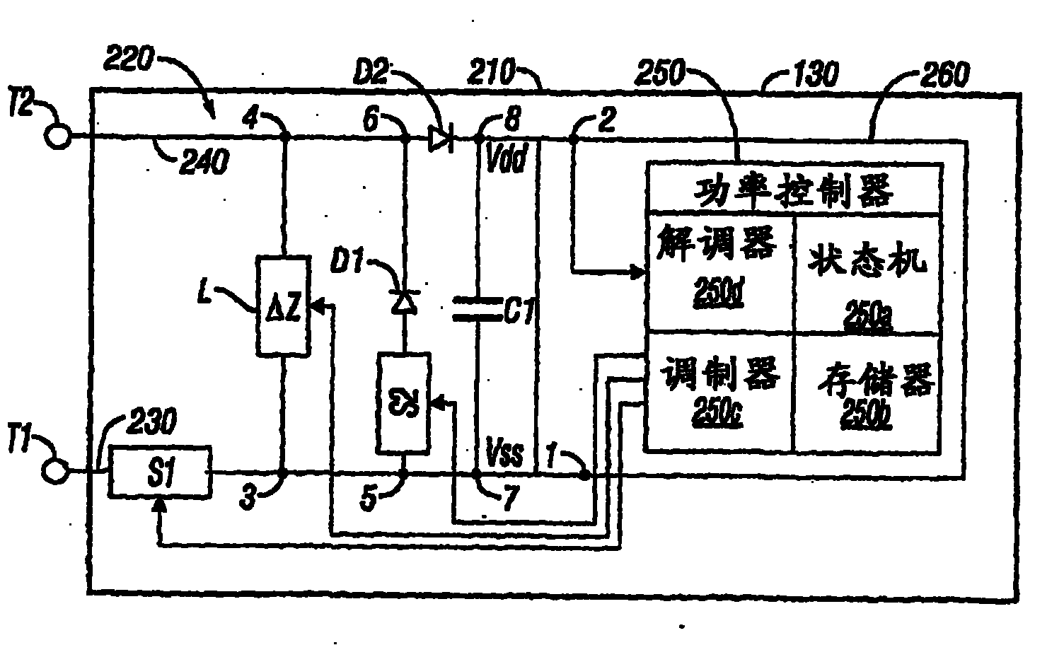
现在详细地参照附图,其中如图1中所示,整个附图中相似的部件可以由相似的附图标记来指示,本发明的无源集成EAS/RFID标签或标记100的组件包括天线110,其是设置成从智能半导体设备130接收能量和信号120以及向智能半导体设备130转发能量和信号120的能量耦合设备。天线110可以用于接收并且转发与标签或标记100相关的能量和信号。天线110可以是用于超高频(UHF)应用的偶极天线并且可以是用于射频(RF)应用的环形天线。实施例在这方面不受限制。将半导体130设计成执行分析和计算功能,这将在下面就图2更详细地解释。天线110经由信号120与半导体设备130操作耦合,并且用作EAS和RFID功能的收发器。尽管在一个实施例中,天线110被显示为与半导体设备130分离,但是天线110也可以作为一个集成单元形成在半导体设备130上。实施例在这方面不受限制。Referring now in detail to the drawings, wherein as shown in FIG. , which is an energy coupling device arranged to receive energy and signals 120 from and forward energy and signals 120 to the
半导体设备130包括内置的双功能电路,用于分别控制EAS和RFID功能。控制EAS/RFID功能的电路可以共享相同(或者相同的部分)电路或者与共同组件,例如天线110耦合。如后面所述,在一个特别的实施例中,可以设计常用于整流(通常非线性)的二极管来实现某些EAS功能,例如混合和谐波产生。还可以设计读取器与EAS或RFID设备/功能的任一个(或者两者)合作。在申请日为2004年11月18日、标题为“INTEGRATED 13.56MHz EAS/RFID DEVICE”的共同拥有的美国临时专利申请第60/629,571号、现在同时申请的标题为“EASREADER DETECTING EAS FUNCTION FROM RFID DEVICE”的PCT专利申请第[代理案卷No.F-TP-00018US/WO]号中公开这种读取器,这两篇专利全部内容在这里通过引用而并入。The
半导体设备130必须被完全供电,以便执行各种RFID应用所需的逻辑运算,例如存取控制、文档跟踪、家畜跟踪、产品认证、零售任务和供应链任务。EAS设备的主要功能是,响应系统询问而产生唯一签名(优选实现而不完全激活附近的RFID标签或标记的RFID逻辑功能)。结果,有效EAS读取范围大于有效RFID读取范围,并且EAS设备/功能趋向于对屏蔽和去谐效应更有弹性。
可以理解,一旦购买了物品或者因为隐私和/或与商店中其它EAS/RFID操作设备干扰的原因设备离开了前提,使EAS/RFID设备失活或失效是重要的。另外,存在已经购买了具有RFID标识的消费者比较喜欢他们的个人信息保持隐密的情况。为此,RFID设备非常适于通过建立标准协议来设置不同的安全级别,即,可以通过RFID设备的能力来实现EAS功能的失活。It will be appreciated that it is important to deactivate or disable the EAS/RFID device once the item is purchased or the device leaves the premises for reasons of privacy and/or interference with other EAS/RFID operating devices in the store. In addition, there are situations where consumers who have purchased tags with RFID prefer that their personal information remain private. For this reason, RFID devices are very suitable for setting different security levels by establishing standard protocols, that is, the inactivation of the EAS function can be realized through the capabilities of RFID devices.
图2A显示了根据本发明的集成EAS/RFID半导体设备130的一个具体例子,其在适于RFID应用的UHF频带具有EAS功能失活能力。半导体设备130安装在基底210上。半导体设备130包括电流接收前端部分220,它还可以用作EAS/RFID半导体设备130的整流前端部分。前端部分220通常在结点1和2处与执行多个RFID功能的EAS/RFID半导体设备130的另一个或者后端部分耦合。前端部分220在端子T1和T2处与天线110耦合。端子T1耦合天线110与源电极230,而端子T2耦合天线110与漏电极240。分别在结点3和4处与电极230和240并联耦合可变或可调阻抗ΔZ。分别在结点5和6处与电极230和240并联耦合二极管D1。相似地,分别在结点7和8处与电极230和240并联耦合电容C1。结点7处的源电压Vss和结点8处的漏电压Vdd通过电容C1提供了储备能量。FIG. 2A shows a specific example of an integrated EAS/
在一个实施例中,设备的EAS部分220基于集成EAS/RFID设备130的前端220的非线性,来混合UHF(超高频)信号和射频(RF)电场。更具体地说,在申请日为2005年6月3日、标题为“TECHNIQUESFOR DETECTING RFID TAGS IN ELECTRONIC ARTICLESURVEILLANCE SYSTEMS USING FREQUENCY MIXING”的共同拥有的待审美国专利申请第11/144,883号中描述了此类实施例,该专利全部内容在这里通过引用而并入。In one embodiment, the
对于EAS功能的失活,将至少一个开关S1和S2插入前端部分220中。具体地,开关S1位于端子T1和结点3之间的源电极230中,并且与端子T1和结点3耦合。因此,因为开关S1位于调制阻抗ΔZ、二极管D1和电容C1上游的源电极230上,开关S1控制流向整个半导体设备130的电流。在一个实施例中,开关S2位于源电极230上的结点5和二极管D1之间并且与源电极230和二极管D1耦合。因此,开关S2控制流过二极管D1的电流。For deactivation of the EAS function, at least one switch S1 and S2 is inserted into the
设计开关S1和S2具有某些基本特性,例如预置存储器和可编程元件。可以在设备有效(加电)期间设置开关的导通状态(例如通/断、低阻/高阻),并且当半导体设备130处于断电状态时维持。由RFID后端部分260经由功率控制器250来提供编程功能,功率控制器250包括至少一个状态机250a(其是执行逻辑运算的开关设备)、存储器250b、调制器250c和解调器250d。调制器250c与调制阻抗ΔZ、开关S1和开关S2耦合。漏电极240在结点2处与解调器250d耦合。状态机250a确定开关S1和S2及调制阻抗ΔZ的操作状态并且控制开关S1和S2及调制阻抗ΔZ。操作状态存储在存储器250b中。状态机250a还通过调制器250c来控制开关S1和S2及调制阻抗ΔZ。典型地通过电容C1向功率控制器250提供能量。Switches S1 and S2 are designed with some basic features such as preset memory and programmable elements. The conduction state (eg on/off, low resistance/high resistance) of the switch may be set during device active (power up) and maintained when the
一旦接通开关S2连同开关S1,电阻充分降低以最大化EAS/RFID标记100的灵敏度。一旦关断开关S1或S2,电阻显著增加,使EAS功能灵敏度降低。另外,设计半导体130,使得RFID设备功能不同地取决于哪个开关被关断。例如,当关断开关S1时,因为开关S1控制从端子T1流向源电极230的电流,半导体设备130的RFID功能260失效。相反,因为开关S2只控制流过二极管D1的电流,所以如果关断S2,只发生RFID功能260的RFID性能或者功能降低。存储器250b可以包括例如程序存储器、数据存储器或者它们的任意组合。存储器250b还可以包括例如随机存取存储器(RAM)、只读存储器(ROM)、可编程只读存储器(PROM)、可擦除可编程只读存储器(EPROM)、电可擦除可编程只读存储器(EEPROM)或者它们的组合等等。Once switch S2 is turned on along with switch S1 , the resistance decreases sufficiently to maximize the sensitivity of EAS/RFID tag 100 . Once the switch S1 or S2 is turned off, the resistance increases significantly, making the EAS function less sensitive. Additionally, the
图2B显示了根据本发明的集成EAS/RFID半导体设备的一个具体例子,其在适于RFID应用的RF频带范围具有EAS功能失活能力。更具体地说,除了将半导体设备130’安装在也包括电流接收前端部分220’的基底210’上之外,半导体设备130’与半导体设备130相同。前端部分220’与半导体设备130的前端部分220之间的差异在于,开关S2不再在结点5和6之间与二极管D1串联耦合。相反,开关S2现在跨越端子T1和T2耦合。此外,电容C2也跨越端子T1和T2与开关S2串联耦合。前端部分220’还用作EAS/RFID半导体设备130’的整流前端部分。电容C2能够将调制阻抗ΔZ所控制的前端部分220’的谐振频率与询问信号120的频率调谐或者频率匹配(参见图1)。FIG. 2B shows a specific example of an integrated EAS/RFID semiconductor device according to the present invention, which has EAS function deactivation capability in the RF frequency band range suitable for RFID applications. More specifically, the semiconductor device 130' is the same as the
典型地,当将商品从失活位置带向EAS系统所在的出口点时,通常发生对集成标记100的功率损失。EAS功能失活的有效性直接与开关S1和S2的通/断电阻比RR的数值成正比,RR由关断位置的开关电阻Roff除以接通位置的开关电阻Ron来定义,或RR=Roff/Ron。Typically, a loss of power to the integrated marker 100 typically occurs when merchandise is brought from the deactivation location to the exit point where the EAS system is located. The effectiveness of the EAS function inactivation is directly proportional to the value of the on/off resistance ratio RR of switches S1 and S2, RR is defined by the switch resistance R off in the off position divided by the switch resistance R on in the on position, or RR =R off /R on .
一个提供用作开关S1和S2的开关功能性能的预期设备与非易失闪存设备(或者浮栅设备)相似,如图3中所示。更具体地说,图3显示了用来控制沟道电阻的浮栅/埋栅设备300的示意图。设备300可以设计为金属氧化物半导体场效应晶体管(MOSFET)设备,其包括与源电极320和漏电极330处于共面取向的基底(或者绝缘层)310。浮栅340位于控制栅350和基底310上的源电极320及漏电极330之间。设备300是具有浮栅340的MOSFET设备。已知场效应晶体管沟道的导电特性取决于栅结构或岛上的电荷量。可以通过Fowler-Nordheim隧穿360a或者沟道热电子注入(CHE)360b来实施这种岛上的电荷注入。一旦注入了电荷360a或360b,电荷可以多年保持在适当状态而没有状态改变。One contemplated device that provides switching functional performance for use as switches S1 and S2 is similar to a non-volatile flash memory device (or a floating gate device), as shown in FIG. 3 . More specifically, FIG. 3 shows a schematic diagram of a floating/buried
对于MOSFET设备,沟道电阻取决于设备的结构和组成,如下面的等式(1)中所示:For MOSFET devices, the channel resistance depends on the structure and composition of the device, as shown in equation (1) below:
其中in
R=沟道电阻,单位欧姆(Ω);R = channel resistance, unit ohm (Ω);
Z=沟道宽度,单位微米(μm);Z = channel width, in microns (μm);
L=沟道长度,单位微米(μm);L = channel length, in microns (μm);
Ci=单位面积绝缘层电容,单位法拉弟/cm2;C i = insulation layer capacitance per unit area, unit Faraday/cm 2 ;
μ=电荷载体迁移率,单位cm2/Volt-sec;以及μ = charge carrier mobility in cm 2 /Volt-sec; and
VG和VT分别是有效栅电压(单位伏)和阈值电压(单位伏),其中,VT取决于设备的组成以及S1和S2的状态。 VG and VT are the effective gate voltage (in volts) and threshold voltage (in volts), respectively, where VT depends on the composition of the device and the state of S1 and S2.
假定RFID部分260仍运行,简单地通过将电荷360a或360b注入浮栅设备340,或者经由地线370从浮栅设备340排出电荷360a或360b,失活或失效过程是可逆的。结果,前述MOSFET设备300可以用作任一个开关S1或S2的接通和关断功能。The deactivation or failure process is reversible simply by injecting
功率控制器250可以控制任何浮栅设备,例如浮栅设备300。可以跨越端子T1和T2耦合一个终止设备(kill device),例如模拟终止设备,并且可以控制阻抗和损失和读取范围以及一些RFID功能。经由结点2向解调器250d输入数据,并且将数据从调制器250c直接输出到开关S1、调制阻抗ΔZ和开关S2。开关S1或S2短路有多好确定了电阻比RR的可能数值。
本发明的实施例可以预期为专用硬件,例如电路、专用集成电路(ASIC)、可编程序逻辑设备(PLD)或者数字信号处理器(DSP)。在再另一个实施例中,可以使用编程的通用计算机组件和客户硬件组件的任意组合来设计标记100、半导体130或读取器硬件。实施例在这方面不受限制。Embodiments of the invention are contemplated as dedicated hardware, such as circuits, application specific integrated circuits (ASICs), programmable logic devices (PLDs), or digital signal processors (DSPs). In yet another embodiment, tag 100,
当如本文中所述已经阐述了本发明实施例的一些特征时,现在对于本领域技术人员会发生许多修改、替换、改变和等价物。因此,应当理解,所附权利要求书打算涵盖所有此类修改和改变,如同它们落在本发明实施例的真实精神内。While some of the features of the embodiments of the invention have been set forth herein, numerous modifications, substitutions, changes and equivalents will now occur to those skilled in the art. It is, therefore, to be understood that the appended claims are intended to cover all such modifications and changes as they fall within the true spirit of the embodiments of this invention.
Claims (13)
Applications Claiming Priority (3)
| Application Number | Priority Date | Filing Date | Title |
|---|---|---|---|
| US63035104P | 2004-11-23 | 2004-11-23 | |
| US60/630,351 | 2004-11-23 | ||
| PCT/US2005/041679 WO2006057888A1 (en) | 2004-11-23 | 2005-11-18 | An integrated eas/rfid device and disabling devices therefor |
Publications (2)
| Publication Number | Publication Date |
|---|---|
| CN101099167A CN101099167A (en) | 2008-01-02 |
| CN101099167B true CN101099167B (en) | 2010-04-14 |
Family
ID=35966379
Family Applications (1)
| Application Number | Title | Priority Date | Filing Date |
|---|---|---|---|
| CN2005800460432A Expired - Fee Related CN101099167B (en) | 2004-11-23 | 2005-11-18 | Integrated EAS/RFID device and disabling device therefor |
Country Status (10)
| Country | Link |
|---|---|
| US (1) | US20080204247A1 (en) |
| EP (1) | EP1815408A1 (en) |
| JP (1) | JP4991558B2 (en) |
| KR (1) | KR101107823B1 (en) |
| CN (1) | CN101099167B (en) |
| AU (1) | AU2005309793B2 (en) |
| BR (1) | BRPI0518049A (en) |
| CA (1) | CA2588556C (en) |
| MX (1) | MX2007006210A (en) |
| WO (1) | WO2006057888A1 (en) |
Families Citing this family (20)
| Publication number | Priority date | Publication date | Assignee | Title |
|---|---|---|---|---|
| WO2008045570A2 (en) | 2006-10-11 | 2008-04-17 | Kovio, Inc. | Multi-mode tags and methods of making and using the same |
| US20080266101A1 (en) * | 2007-04-27 | 2008-10-30 | Sensormatic Electronics Corporation | Security tag sensor and seccurity meethod for capital assets |
| US8633821B2 (en) | 2007-12-03 | 2014-01-21 | Avery Dennison Corporation | Dual use RFID/EAS device |
| US8144018B1 (en) * | 2008-03-06 | 2012-03-27 | Sensormatic Electronics, LLC | Combination electronic article surveillance/radio frequency identification antenna and method |
| KR100942706B1 (en) * | 2008-08-22 | 2010-02-16 | 한국전자통신연구원 | Rfid system using human body communication |
| KR101041217B1 (en) * | 2008-12-08 | 2011-06-13 | 학교법인 동의학원 | RFS-based EAS system |
| US20100140351A1 (en) * | 2008-12-08 | 2010-06-10 | Sentry Technology Corporation | Method for preventing article theft and self-checkout system carrying out the method |
| US20100148965A1 (en) * | 2008-12-16 | 2010-06-17 | Sensormatic Electronics Corporation | Method and system for item level uhf rfid tag with low frequency power assist |
| US8648721B2 (en) * | 2010-08-09 | 2014-02-11 | Tyco Fire & Security Gmbh | Security tag with integrated EAS and energy harvesting magnetic element |
| US9342775B2 (en) | 2011-11-01 | 2016-05-17 | Avery Dennison Corporation | Dual mode chip having radio frequency identification and electronic article surveillance capability |
| US8917179B2 (en) * | 2012-03-30 | 2014-12-23 | Tyco Fire & Security Gmbh | System and method for detecting presence of an object |
| EP2759975B1 (en) * | 2013-01-24 | 2017-06-07 | Nxp B.V. | Tag system, sellable item and method for facilitating the purchase of a sellable item |
| DE112013007562T5 (en) * | 2013-10-31 | 2016-07-21 | Mitsubishi Electric Engineering Company, Limited | Resonant type high frequency power supply device and circuit for a resonant type high frequency power supply device |
| KR20160078392A (en) * | 2013-10-31 | 2016-07-04 | 미쓰비시 덴끼 엔지니어링 가부시키가이샤 | Resonant high-frequency power supply device and switching circuit for resonant high-frequency power supply device |
| JPWO2015063920A1 (en) * | 2013-10-31 | 2017-03-09 | 三菱電機エンジニアリング株式会社 | Resonant type high frequency power supply |
| WO2015063921A1 (en) * | 2013-10-31 | 2015-05-07 | 三菱電機エンジニアリング株式会社 | Resonant high frequency power source device |
| CN108363932B (en) * | 2017-01-26 | 2023-04-18 | 手持产品公司 | Method for reading bar code and deactivating electronic anti-theft label of commodity |
| US10210731B2 (en) | 2017-06-28 | 2019-02-19 | Datalogic IP Tech, S.r.l. | Systems and methods for a smart electronic article surveillance circuit |
| US10380857B1 (en) | 2018-03-05 | 2019-08-13 | Sensormatic Electronics, LLC | Systems and methods for radio frequency identification enabled deactivation of acousto-magnetic ferrite based marker |
| EP3871202B1 (en) * | 2018-10-25 | 2024-08-14 | Sensormatic Electronics LLC | Unified security device |
Citations (4)
| Publication number | Priority date | Publication date | Assignee | Title |
|---|---|---|---|---|
| US5955951A (en) * | 1998-04-24 | 1999-09-21 | Sensormatic Electronics Corporation | Combined article surveillance and product identification system |
| WO2000016289A1 (en) * | 1998-09-11 | 2000-03-23 | Motorola Inc. | Electrostatic rfid/eas system |
| CN1349639A (en) * | 1999-05-04 | 2002-05-15 | 传感电子公司 | Self-checkout/self-check-in RFID and electronic article surveillance system |
| CN1392998A (en) * | 2000-09-19 | 2003-01-22 | 穆尔北美公司 | RFID composite for mounting on metal object |
Family Cites Families (22)
| Publication number | Priority date | Publication date | Assignee | Title |
|---|---|---|---|---|
| US4745401A (en) * | 1985-09-09 | 1988-05-17 | Minnesota Mining And Manufacturing Company | RF reactivatable marker for electronic article surveillance system |
| US5939984A (en) * | 1997-12-31 | 1999-08-17 | Intermec Ip Corp. | Combination radio frequency transponder (RF Tag) and magnetic electronic article surveillance (EAS) material |
| US6208235B1 (en) * | 1997-03-24 | 2001-03-27 | Checkpoint Systems, Inc. | Apparatus for magnetically decoupling an RFID tag |
| US5963144A (en) * | 1997-05-30 | 1999-10-05 | Single Chip Systems Corp. | Cloaking circuit for use in a radiofrequency identification and method of cloaking RFID tags to increase interrogation reliability |
| US6025780A (en) * | 1997-07-25 | 2000-02-15 | Checkpoint Systems, Inc. | RFID tags which are virtually activated and/or deactivated and apparatus and methods of using same in an electronic security system |
| WO1999030432A1 (en) * | 1997-12-05 | 1999-06-17 | Koninklijke Philips Electronics N.V. | Identification transponder |
| SG79961A1 (en) * | 1998-02-07 | 2001-04-17 | Ct For Wireless Communications | A rectifying antenna circuit |
| JP3264266B2 (en) * | 1998-06-04 | 2002-03-11 | 三菱マテリアル株式会社 | Anti-theft tag and method of using the same |
| DE69942811D1 (en) * | 1998-08-14 | 2010-11-11 | 3M Innovative Properties Co | Applications for radio frequency information systems |
| JP3359608B2 (en) * | 1999-02-19 | 2002-12-24 | 日本電信電話株式会社 | Non-contact IC card system |
| DE60037989T2 (en) * | 1999-09-22 | 2009-02-26 | Em Microelectronic-Marin S.A., Marin | Transponder for different purposes |
| DE60042065D1 (en) * | 2000-01-17 | 2009-06-04 | Nxp Bv | DATA CARRIER WITH ADJUSTABLE SIGNAL RECEPTION ARRANGEMENT |
| US6356197B1 (en) * | 2000-04-03 | 2002-03-12 | Sensormatic Electronics Corporation | Electronic article surveillance and identification device, system, and method |
| JP2001357369A (en) * | 2000-06-13 | 2001-12-26 | Denso Corp | Ic chip for mounting ic card or the like |
| JP3607585B2 (en) * | 2000-08-23 | 2005-01-05 | 日本電信電話株式会社 | Non-contact response device |
| US7006014B1 (en) * | 2000-10-17 | 2006-02-28 | Henty David L | Computer system with passive wireless keyboard |
| US6434372B1 (en) * | 2001-01-12 | 2002-08-13 | The Regents Of The University Of California | Long-range, full-duplex, modulated-reflector cell phone for voice/data transmission |
| US7079020B2 (en) * | 2003-02-03 | 2006-07-18 | Ingrid, Inc. | Multi-controller security network |
| US6836159B2 (en) * | 2003-03-06 | 2004-12-28 | General Electric Company | Integrated high-voltage switching circuit for ultrasound transducer array |
| US7026935B2 (en) * | 2003-11-10 | 2006-04-11 | Impinj, Inc. | Method and apparatus to configure an RFID system to be adaptable to a plurality of environmental conditions |
| US7109867B2 (en) * | 2004-09-09 | 2006-09-19 | Avery Dennison Corporation | RFID tags with EAS deactivation ability |
| WO2008045570A2 (en) * | 2006-10-11 | 2008-04-17 | Kovio, Inc. | Multi-mode tags and methods of making and using the same |
-
2005
- 2005-11-18 CN CN2005800460432A patent/CN101099167B/en not_active Expired - Fee Related
- 2005-11-18 WO PCT/US2005/041679 patent/WO2006057888A1/en not_active Ceased
- 2005-11-18 BR BRPI0518049-0A patent/BRPI0518049A/en not_active IP Right Cessation
- 2005-11-18 US US11/791,089 patent/US20080204247A1/en not_active Abandoned
- 2005-11-18 KR KR1020077014085A patent/KR101107823B1/en not_active Expired - Fee Related
- 2005-11-18 JP JP2007543235A patent/JP4991558B2/en not_active Expired - Fee Related
- 2005-11-18 CA CA2588556A patent/CA2588556C/en not_active Expired - Fee Related
- 2005-11-18 AU AU2005309793A patent/AU2005309793B2/en not_active Ceased
- 2005-11-18 EP EP20050826479 patent/EP1815408A1/en not_active Withdrawn
- 2005-11-18 MX MX2007006210A patent/MX2007006210A/en active IP Right Grant
Patent Citations (4)
| Publication number | Priority date | Publication date | Assignee | Title |
|---|---|---|---|---|
| US5955951A (en) * | 1998-04-24 | 1999-09-21 | Sensormatic Electronics Corporation | Combined article surveillance and product identification system |
| WO2000016289A1 (en) * | 1998-09-11 | 2000-03-23 | Motorola Inc. | Electrostatic rfid/eas system |
| CN1349639A (en) * | 1999-05-04 | 2002-05-15 | 传感电子公司 | Self-checkout/self-check-in RFID and electronic article surveillance system |
| CN1392998A (en) * | 2000-09-19 | 2003-01-22 | 穆尔北美公司 | RFID composite for mounting on metal object |
Also Published As
| Publication number | Publication date |
|---|---|
| CA2588556A1 (en) | 2006-06-01 |
| US20080204247A1 (en) | 2008-08-28 |
| KR101107823B1 (en) | 2012-02-08 |
| KR20070097456A (en) | 2007-10-04 |
| JP2008523461A (en) | 2008-07-03 |
| HK1114217A1 (en) | 2008-10-24 |
| EP1815408A1 (en) | 2007-08-08 |
| WO2006057888A1 (en) | 2006-06-01 |
| CA2588556C (en) | 2011-05-31 |
| CN101099167A (en) | 2008-01-02 |
| MX2007006210A (en) | 2008-02-19 |
| AU2005309793B2 (en) | 2009-10-01 |
| AU2005309793A1 (en) | 2006-06-01 |
| BRPI0518049A (en) | 2008-10-28 |
| JP4991558B2 (en) | 2012-08-01 |
Similar Documents
| Publication | Publication Date | Title |
|---|---|---|
| CN101099167B (en) | Integrated EAS/RFID device and disabling device therefor | |
| US8174388B2 (en) | Method and system for deactivation of combination EAS/RFID tags | |
| US8633821B2 (en) | Dual use RFID/EAS device | |
| JP4766437B2 (en) | Multi-mode tags and methods for making and using multi-mode tags | |
| AU723295B2 (en) | Apparatus for magnetically decoupling an RFID tag | |
| US7321290B2 (en) | Radio tag and system | |
| US7986241B2 (en) | Combination security tag using a perimeter RFID antenna surrounding an EAS element and method thereof | |
| US20130105584A1 (en) | Dual mode chip having radio frequency identification and electronic article surveillance capability | |
| JP2011118934A (en) | Electronic apparatus | |
| US8026819B2 (en) | Radio tag and system | |
| HK1114217B (en) | An integrated eas/rfid device and disabling devices therefor | |
| HK1167197B (en) | Method and system for deactivation of combination eas/rfid tags |
Legal Events
| Date | Code | Title | Description |
|---|---|---|---|
| C06 | Publication | ||
| PB01 | Publication | ||
| C10 | Entry into substantive examination | ||
| SE01 | Entry into force of request for substantive examination | ||
| REG | Reference to a national code |
Ref country code: HK Ref legal event code: DE Ref document number: 1114217 Country of ref document: HK |
|
| C14 | Grant of patent or utility model | ||
| GR01 | Patent grant | ||
| REG | Reference to a national code |
Ref country code: HK Ref legal event code: GR Ref document number: 1114217 Country of ref document: HK |
|
| ASS | Succession or assignment of patent right |
Owner name: SENSOR ELECTRONICS CO., LTD. Free format text: FORMER OWNER: SENSORMATIC ELECTRONICS CORPORATION Effective date: 20150811 Owner name: ADT SERVICE LLC Free format text: FORMER OWNER: SENSOR ELECTRONICS CO., LTD. Effective date: 20150811 Owner name: TYCO FIRE + SECURITY GMBH Free format text: FORMER OWNER: ADT SERVICE LLC Effective date: 20150811 |
|
| C41 | Transfer of patent application or patent right or utility model | ||
| TR01 | Transfer of patent right |
Effective date of registration: 20150811 Address after: Switzerland Rhine falls Neuhausen Patentee after: TYCO FIRE & SECURITY GmbH Address before: Switzerland Rhine falls Neuhausen Patentee before: ADT Services LLC Effective date of registration: 20150811 Address after: Switzerland Rhine falls Neuhausen Patentee after: ADT Services LLC Address before: American Florida Patentee before: SENSORMATIC ELECTRONICS, LLC Effective date of registration: 20150811 Address after: American Florida Patentee after: SENSORMATIC ELECTRONICS, LLC Address before: American Florida Patentee before: SENSORMATIC ELECTRONICS Corp. |
|
| CF01 | Termination of patent right due to non-payment of annual fee |
Granted publication date: 20100414 Termination date: 20151118 |
|
| EXPY | Termination of patent right or utility model |