CN101080023B - Image forming apparatus with a plurality of image forming units - Google Patents
Image forming apparatus with a plurality of image forming units Download PDFInfo
- Publication number
- CN101080023B CN101080023B CN2007101292026A CN200710129202A CN101080023B CN 101080023 B CN101080023 B CN 101080023B CN 2007101292026 A CN2007101292026 A CN 2007101292026A CN 200710129202 A CN200710129202 A CN 200710129202A CN 101080023 B CN101080023 B CN 101080023B
- Authority
- CN
- China
- Prior art keywords
- pixel
- pixels
- color
- interpolation
- correlation
- Prior art date
- Legal status (The legal status is an assumption and is not a legal conclusion. Google has not performed a legal analysis and makes no representation as to the accuracy of the status listed.)
- Expired - Fee Related
Links
Images


Classifications
-
- H—ELECTRICITY
- H04—ELECTRIC COMMUNICATION TECHNIQUE
- H04N—PICTORIAL COMMUNICATION, e.g. TELEVISION
- H04N9/00—Details of colour television systems
- H04N9/64—Circuits for processing colour signals
- H04N9/646—Circuits for processing colour signals for image enhancement, e.g. vertical detail restoration, cross-colour elimination, contour correction, chrominance trapping filters
-
- H—ELECTRICITY
- H04—ELECTRIC COMMUNICATION TECHNIQUE
- H04N—PICTORIAL COMMUNICATION, e.g. TELEVISION
- H04N23/00—Cameras or camera modules comprising electronic image sensors; Control thereof
- H04N23/10—Cameras or camera modules comprising electronic image sensors; Control thereof for generating image signals from different wavelengths
- H04N23/12—Cameras or camera modules comprising electronic image sensors; Control thereof for generating image signals from different wavelengths with one sensor only
-
- H—ELECTRICITY
- H04—ELECTRIC COMMUNICATION TECHNIQUE
- H04N—PICTORIAL COMMUNICATION, e.g. TELEVISION
- H04N23/00—Cameras or camera modules comprising electronic image sensors; Control thereof
- H04N23/80—Camera processing pipelines; Components thereof
- H04N23/84—Camera processing pipelines; Components thereof for processing colour signals
- H04N23/843—Demosaicing, e.g. interpolating colour pixel values
-
- H—ELECTRICITY
- H04—ELECTRIC COMMUNICATION TECHNIQUE
- H04N—PICTORIAL COMMUNICATION, e.g. TELEVISION
- H04N25/00—Circuitry of solid-state image sensors [SSIS]; Control thereof
-
- H—ELECTRICITY
- H04—ELECTRIC COMMUNICATION TECHNIQUE
- H04N—PICTORIAL COMMUNICATION, e.g. TELEVISION
- H04N25/00—Circuitry of solid-state image sensors [SSIS]; Control thereof
- H04N25/10—Circuitry of solid-state image sensors [SSIS]; Control thereof for transforming different wavelengths into image signals
- H04N25/11—Arrangement of colour filter arrays [CFA]; Filter mosaics
- H04N25/13—Arrangement of colour filter arrays [CFA]; Filter mosaics characterised by the spectral characteristics of the filter elements
- H04N25/133—Arrangement of colour filter arrays [CFA]; Filter mosaics characterised by the spectral characteristics of the filter elements including elements passing panchromatic light, e.g. filters passing white light
-
- H—ELECTRICITY
- H04—ELECTRIC COMMUNICATION TECHNIQUE
- H04N—PICTORIAL COMMUNICATION, e.g. TELEVISION
- H04N25/00—Circuitry of solid-state image sensors [SSIS]; Control thereof
- H04N25/10—Circuitry of solid-state image sensors [SSIS]; Control thereof for transforming different wavelengths into image signals
- H04N25/11—Arrangement of colour filter arrays [CFA]; Filter mosaics
- H04N25/13—Arrangement of colour filter arrays [CFA]; Filter mosaics characterised by the spectral characteristics of the filter elements
- H04N25/135—Arrangement of colour filter arrays [CFA]; Filter mosaics characterised by the spectral characteristics of the filter elements based on four or more different wavelength filter elements
-
- H—ELECTRICITY
- H04—ELECTRIC COMMUNICATION TECHNIQUE
- H04N—PICTORIAL COMMUNICATION, e.g. TELEVISION
- H04N2209/00—Details of colour television systems
- H04N2209/04—Picture signal generators
- H04N2209/041—Picture signal generators using solid-state devices
- H04N2209/042—Picture signal generators using solid-state devices having a single pick-up sensor
- H04N2209/045—Picture signal generators using solid-state devices having a single pick-up sensor using mosaic colour filter
- H04N2209/046—Colour interpolation to calculate the missing colour values
Landscapes
- Engineering & Computer Science (AREA)
- Multimedia (AREA)
- Signal Processing (AREA)
- Physics & Mathematics (AREA)
- Spectroscopy & Molecular Physics (AREA)
- Color Television Image Signal Generators (AREA)
Abstract
Description
相关申请的交叉引用Cross References to Related Applications
本发明包括涉及2006年4月14日在日本专利局申请的日本专利申请JP2006-111633的主题,其整个内容一并引用至此。The present invention contains subject matter related to Japanese Patent Application JP2006-111633 filed in the Japan Patent Office on Apr. 14, 2006, the entire content of which is hereby incorporated by reference.
技术领域technical field
本发明涉及在其中处理包括亮度信息的像素的成像装置。The invention relates to an imaging device in which pixels including luminance information are processed.
背景技术Background technique
基于在上部和下部以及左边和右边排列的G(绿色)像素的相关信息(例如参见JP-A-2001-218073),在配置为具有RGB矩形Bayer(拜尔)布局的现有技术的图像传感器中可以执行像素内插(interpolation)。在其中处理包括亮度信息的像素并且布局是相对于矩形倾斜45°的图像传感器中,由于在其上下以及左右没有排列绿色像素,因此不能执行相关技术的像素内插法。因此,用于具有这种像素布局的图像传感器中的像素内插的相关检测通常由相同颜色的平均像素确定。然而,这种内插法具有在高频率下使空间频率平整并产生错误颜色的缺点。这种相关检测方法的另一个缺点是在亮度信号Y和色度信号Cr/Cb的信号处理中可能不能正确执行颜色分离。Based on information on G (green) pixels arranged at the upper and lower and left and right (see, for example, JP-A-2001-218073 ), in a prior art image sensor configured to have an RGB rectangular Bayer (Bayer) layout Can perform pixel interpolation (interpolation). In an image sensor in which pixels including luminance information are processed and the layout is inclined at 45° with respect to a rectangle, since green pixels are not arranged above and below and left and right thereof, pixel interpolation of the related art cannot be performed. Correlative detection for pixel interpolation in image sensors with such a pixel layout is therefore typically determined by the average pixel of the same color. However, this interpolation method has the disadvantage of flattening the spatial frequency at high frequencies and producing false colors. Another disadvantage of this correlation detection method is that color separation may not be performed correctly in the signal processing of the luminance signal Y and chrominance signals Cr/Cb.
发明内容Contents of the invention
将要解决的问题就是在相关检测中在高频率下使空间频率平整并产生错误颜色。另一个将要解决的问题就是在亮度信号Y以及色度信号Cr/Cb的信号处理中不能正确地执行颜色分离。The problem to be solved is flattening the spatial frequencies and producing false colors at high frequencies in correlation detection. Another problem to be solved is that color separation cannot be correctly performed in the signal processing of the luminance signal Y and the chrominance signals Cr/Cb.
合乎需要的是防止在彩色对象中产生的错误颜色并与简单平均像素内插相比扩展该频带。It is desirable to prevent false colors produced in colored objects and to extend the frequency band compared to simple average pixel interpolation.
根据本发明的一个实施例,提供了一种成像装置,包括具有多个彩色像素以及高灵敏度像素的图像传感器,所述高灵敏度像素对入射光具有比以棋盘形图案的方式排列的彩色像素更高的灵敏度;相关性检测器,根据高灵敏度像素的信号分量以及该彩色像素的信号分量来检测成像对象的相关性;彩色判断部件,根据该彩色像素的信号分量判断成像对象是否属于彩色;以及像素内插器,根据在判断对象是否属于彩色的彩色判断部件里判断的信号在像素内插法之间切换。当彩色判断部件断定该对象属于彩色时,基于来自相关性检测器的信息,所述像素内插器将高优先权给予使用示出强相关性的像素的内插。According to one embodiment of the present invention, there is provided an imaging device including an image sensor having a plurality of color pixels and high-sensitivity pixels having a higher sensitivity to incident light than color pixels arranged in a checkerboard pattern. High sensitivity; the correlation detector detects the correlation of the imaging object according to the signal component of the high-sensitivity pixel and the signal component of the color pixel; the color judging part judges whether the imaging object belongs to color according to the signal component of the color pixel; and The pixel interpolator switches between pixel interpolation methods based on a signal judged in the color judging section judging whether an object belongs to a color. When the color judging section judges that the object belongs to color, based on the information from the correlation detector, the pixel interpolator gives high priority to interpolation using pixels showing strong correlation.
在上述本发明的实施例中,提供判断图像对象是否属于彩色的彩色判断部件,以及像素内插器,根据在判断对象是否属于彩色的彩色判断部件里判断的信号在像素内插法之间切换,当彩色判断部件断定对象属于彩色时,基于来自相关性检测器的信息,所述像素内插器将高优先权给予使用示出强相关性的像素的内插。彩色判断部件以及像素内插器的提供可以允许彩色像素的内插。In the embodiment of the present invention described above, a color judging part for judging whether an image object belongs to a color is provided, and a pixel interpolator for switching between pixel interpolation methods according to a signal judged in the color judging part for judging whether an object belongs to a color , when the color judging section judges that the object belongs to the color, based on the information from the correlation detector, the pixel interpolator gives high priority to interpolation using pixels showing strong correlation. The provision of a color determination component and a pixel interpolator may allow interpolation of color pixels.
根据本发明的上述实施例,基于来自相关性检测器的信息,将高优先权给予使用示出强相关性的像素的内插的像素内插器的提供可以允许彩色像素的内插,从而提供了与简单平均像素内插相比扩展的频带的优点。此外,这里还提供了与简单平均像素内插相比在彩色对象中抑制错误颜色的另一个优点。According to the above-described embodiments of the present invention, the provision of a pixel interpolator that gives high priority to interpolation using pixels showing strong correlations based on information from the correlation detector may allow interpolation of colored pixels, thereby providing advantage of the extended frequency band compared to simple average pixel interpolation. Furthermore, another advantage of suppressing false colors in colored objects compared to simple average pixel interpolation is provided here.
附图说明Description of drawings
附图1是示出根据本发明实施例(第一实例)成像装置的方框图;Accompanying
附图2是示出像素内插块详情的实例的方框图;Figure 2 is a block diagram illustrating an example of details of a pixel interpolation block;
附图3是示出内插器A的实例的方框图;
附图4是示出内插器A如何执行像素内插的实例的布局图;Figure 4 is a layout diagram showing an example of how interpolator A performs pixel interpolation;
附图5是示出内插器B的实例的方框图;
附图6是示出当相关性分别在水平方向和垂直方向上较强时,内插器B如何执行像素内插的实例的布局图;FIG. 6 is a layout diagram showing an example of how interpolator B performs pixel interpolation when the correlation is strong in the horizontal and vertical directions, respectively;
附图7示出内插B的实例的算法;Accompanying drawing 7 shows the algorithm of the instance of interpolation B;
附图8是示出实施本发明的成像装置的实例的方框图;FIG. 8 is a block diagram showing an example of an imaging device embodying the present invention;
附图9是示出成像装置中传感器的彩色布局的实例的像素布局图;Figure 9 is a pixel layout diagram showing an example of a color layout of a sensor in an imaging device;
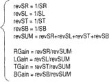
附图10是示出在内插位置的B像素和R像素阵列之间示例性相关系数的布局图;Figure 10 is a layout diagram showing exemplary correlation coefficients between B pixel and R pixel arrays at interpolation positions;
附图11示出相关性检测的实例的算法;
附图12示出相关性系数计算方程式;Accompanying drawing 12 shows correlation coefficient calculation equation;
附图13示出像素内插的实例的算法;Accompanying drawing 13 shows the algorithm of the example of pixel interpolation;
附图14是示出内插位置B像素和G像素阵列之间相关性系数的布局图;Accompanying drawing 14 is a layout diagram showing correlation coefficients between B pixels and G pixel arrays at interpolation positions;
附图15示出相关性检测的实例的算法;Accompanying drawing 15 shows the algorithm of the example of correlation detection;
附图16示出相关性系数计算方程式;Accompanying drawing 16 shows correlation coefficient calculation equation;
附图17示出像素内插的实例的算法;Accompanying drawing 17 shows the algorithm of the example of pixel interpolation;
附图18示出电平平衡之后信号布局的实例的布局图;Accompanying
附图19示出低通滤波器的实例的算法;Accompanying drawing 19 shows the algorithm of the example of low-pass filter;
附图20示出以亮度和色度的形式表示的方程式;Figure 20 shows the equations expressed in terms of luminance and chromaticity;
附图21是示出在W像素出现的位置上R/G/B像素内插的实例的布局图,并且还示出内插方程式;FIG. 21 is a layout diagram showing an example of R/G/B pixel interpolation at a position where a W pixel occurs, and also shows an interpolation equation;
附图22示出使用W像素作为相关性检测信号互补的实例的布局图;Accompanying
附图23是示出在不存在像素的相位上像素互补的实例的布局图;FIG. 23 is a layout diagram showing an example of pixel complementarity on a phase where no pixel exists;
附图24示出其中在水平/垂直方向上低通滤波器施加到W像素的实例的算法;Accompanying drawing 24 shows the algorithm of the example in which low-pass filter is applied to W pixel in horizontal/vertical direction;
附图25示出相关性系数计算方程式;以及Accompanying
附图26示出像素内插的实例的算法。Figure 26 shows the algorithm for an example of pixel interpolation.
具体实施方式Detailed ways
以下将参考图1到9描述根据本发明的实施例(第一实例)。An embodiment (first example) according to the present invention will be described below with reference to FIGS. 1 to 9 .
首先,参考图8的方框图描述实施本发明的成像装置的实例。举例来说,附图8示出了使用图像传感器的整个照相机系统。First, an example of an imaging device embodying the present invention will be described with reference to the block diagram of FIG. 8 . As an example, Figure 8 shows an entire camera system using an image sensor.
如附图8所示,成像装置1包括聚焦图像的透镜系统2,具有用于光电转换的像素的传感器3,接收该电信号、消除1/f噪音并且仅仅提取信号分量的相关双采样(CDS)部件4,将来自传感器的像素信号(其是模拟信号)转换为数字信号的模拟-数字转换器(ADC)5,以及将数字化的传感器信号输出为最后的图像信号的信号处理部件6。As shown in FIG. 8 , an
在成像装置1中,通过透镜系统2聚焦的图像成像到传感器3的像素上并且作为电信号输出到CDS部件4。CDS部件4消除1/f噪音并且仅仅提取信号分量。然后,ADC 5将来自传感器的作为模拟信号的像素信号转换为数字信号。数字化的传感器信号然后被输入到信号处理部件6并且处理为最终的图像信号。In the
接下来,将参考附图9描述成像装置1中传感器3彩色布局的实例。Next, an example of the color layout of the
如附图9所示,在传感器3中的彩色布局中,相对于现有技术的RGB矩形Bayer像素布局,用于获得亮度信息的像素(在本实例中,具有比彩色像素更高的入射光灵敏度的高灵敏度像素)排列在具有偏移半个周期的空间相位的相位位置上。高灵敏度像素例如由白色像素或灰色像素形成。以下将参考排列了白色(W)像素的示例来作出描述。As shown in accompanying drawing 9, in the color layout in
现在将描述本发明主要特点。附图1是示出信号处理部件6的细节的方框图。附图2是示出附图1所示的照相机系统信号处理器中的像素内插部件13内部组件的方框图。The main features of the present invention will now be described. FIG. 1 is a block diagram showing details of the
如附图1所示,来自传感器已经通过模拟-数字转换器(ADC)转化为数字信号的像素信号输入到白平衡(WB)部件11,其中从传感器输出的该像素相对于作为彩色像素的G(绿色)像素或作为高灵敏度像素的W像素被校正(normalized,标准化)。在这个实例中,尽管举例来说输出的像素根据W像素校正,但是输出的像素还可以根据灰色像素校正。以下将参考W像素作出描述。As shown in FIG. 1, a pixel signal from a sensor that has been converted into a digital signal by an analog-to-digital converter (ADC) is input to a white balance (WB)
校正信号输入到互相独立的彩色判断部件12和像素内插部件13。彩色判断部件12判断所关心的像素以及周围像素是否是彩色像素并且将结果发送给像素内插部件13。The correction signal is input to the color judging section 12 and the pixel interpolating section 13 which are independent from each other. The color judgment section 12 judges whether the pixel of interest and surrounding pixels are color pixels and sends the result to the pixel interpolation section 13 .
通过内插两个缺乏的颜色,像素内插部件13在出现R/G/B像素中的一个的相位上的执行内插。例如,B/R像素用于其中出现G像素位置上的内插。像素内插部件13使用彩色判断部件12的判断结果动态地变化内插处理。当所关心的像素不是彩色像素时,当产生用于内插的像素时来自所关心的像素的像素信号必定用于改善分辨率,而当所关心的像素是彩色像素时,来自具有如将用于内插的像素的相同颜色的周围像素的信号被内插。像素内插之后处理被分成两条线,即产生亮度和产生色度。首先描述产生亮度的处理线。By interpolating two missing colors, the pixel interpolation section 13 performs interpolation on a phase in which one of the R/G/B pixels appears. For example, B/R pixels are used for interpolation at positions where G pixels occur. The pixel interpolation section 13 dynamically changes the interpolation process using the judgment result of the color judgment section 12 . When the pixel of interest is not a color pixel, the pixel signal from the pixel of interest must be used to improve the resolution when generating the pixel for interpolation, while when the pixel of interest is a color pixel, the The signals of surrounding pixels of the same color as the interpolated pixel are interpolated. Processing after pixel interpolation is split into two lines, luma generation and chrominance generation. First, the processing line that produces luminance will be described.
在像素内插部件13中产生的R/G/B像素信号经历转换过程,诸如作为典型实例NTSC亮度转换方程式,以便产生Y信号。由于产生的Y信号和W像素就信号电平而言互相不匹配,因此在电平平衡部件14中执行电平匹配。电平平衡部件14产生(高频)亮度信号,在其中的W信号的电平和Y信号的电平相同。The R/G/B pixel signal generated in the pixel interpolation section 13 is subjected to a conversion process such as an NTSC luminance conversion equation as a typical example to generate a Y signal. Since the generated Y signal and W pixel do not match each other in terms of signal levels, level matching is performed in the level balancing section 14 . The level balancing section 14 generates a (high frequency) luminance signal in which the level of the W signal is the same as that of the Y signal.
然而,由于具有亮度信号的像素和不具有亮度信号的像素是在空间排列而且交替地出现(就空间相位而言是1/2),因此其中不存在像素的相位通过像素补充。这种互补是在亮度内插部件16中执行。这种互补处理的判断在相关检测部件15中执行。相关检测部件15通过使用亮度信号作为检测信号执行这种处理。检测结果既可以在亮度产生也可以在色度产生中使用。However, since pixels with a luminance signal and pixels without a luminance signal are spatially arranged and appear alternately (1/2 in terms of spatial phase), phases in which there are no pixels are supplemented by pixels. This complementation is performed in the luminance interpolation section 16 . Judgment of such complementary processing is performed in the correlation detection section 15 . The correlation detection section 15 performs such processing by using the luminance signal as a detection signal. Detection results can be used in both luma and chrominance generation.
在色度内插部件17中,R/G/B像素首先用于在出现W像素的相位上的内插。这种内插例如通过计算周围W像素和R/G/B像素的比率来计算。此外,为执行在空间上不存在R/G/B像素的相位上的像素互补,相关检测部件15的检测结果(其已经在亮度产生中描述)反映像素互补。In the chroma interpolation section 17, the R/G/B pixels are first used for interpolation at the phase in which the W pixels appear. This interpolation is calculated, for example, by calculating the ratio of surrounding W pixels and R/G/B pixels. Furthermore, to perform pixel complementation on a phase where R/G/B pixels do not spatially exist, the detection result of the correlation detection section 15, which has been described in luminance generation, reflects pixel complementarity.
亮度内插部件18是将高频亮度信号和在色度产生处理中计算的R/G/B信号结合起来产生低频Y亮度信号。这种处理抑制了在低频区亮度再生中的退化。The
因此产生Y/Cr/Cb信号并且结束像素内插。Thus Y/Cr/Cb signals are generated and pixel interpolation ends.
举例来说,如附图2所示的像素内插部件13的元件包括识别内插相位处像素的彩色滤波器的彩色识别部件21和将信号引导给适当的内插处理中的一个(例如内插器A 23或内插器B 24)的多路复用器(MPX)22。By way of example, elements of the pixel interpolation section 13 shown in FIG. Multiplexer (MPX) 22 of
接下来,参考附图3、4A和4B描述在内插相位处像素彩色滤波器是R(红)或B(蓝色)的情况中执行的内插处理(例如内插器A 23)。附图3是内插器A 23的方框图,而附图4是示出内插器A 23如何执行像素内插的概念图。Next, interpolation processing (for example, interpolator A 23) performed in the case where the pixel color filter at the interpolation phase is R (red) or B (blue) is described with reference to FIGS. 3 , 4A, and 4B. FIG. 3 is a block diagram of
如附图4所示,在将被内插的相位的像素是B像素,而用于内插的像素是R和G像素。由于用于内插的R像素位于相对于B像素的四个对角线方向(参见附图4中的(1)),附图3所示的相关性检测器25用于执行这种对角线方向中的相关检测,而像素内插器26用于根据从相关检测器25输出的相关强度改变四个方向中的R像素的混合比率,以便执行R像素的内插。G像素可以同样处理。从四个上/下和左/右方向(参见附图4中的(2)),附图3所示的相关性检测器27用于执行水平方向和垂直方向的相关检测,像素内插器28通过使用四个方向中G像素混合比率根据来自相关性检测器27输出的相关检测结果执行G像素的内插。As shown in FIG. 4, the pixels at the phase to be interpolated are B pixels, and the pixels used for interpolation are R and G pixels. Since the R pixels used for interpolation are located in four diagonal directions (see (1) in FIG. 4 ) with respect to the B pixels, the
当在内插相位的像素是R时,除了B替换为R而R替换为B之外可以适用于同样的处理。也就是说,在内插相位的像素是R像素,而用于内插的像素是B和G像素。由于可以用于内插的B像素位于相对于R像素的四个对角线方向,在对角线方向执行相关检测并且根据相关强度改变四个方向中的B像素混合比率以便执行B像素的内插。G像素可以同样处理。通过使用四个方向中的G像素的混合比率,G像素的内插根据由四个上/下和左/右方向的相关检测结果执行。When the pixel of the interpolated phase is R, the same process can be applied except that B is replaced by R and R is replaced by B. That is, the pixels in the interpolation phase are R pixels, and the pixels used for interpolation are B and G pixels. Since the B pixels that can be used for interpolation are located in the four diagonal directions with respect to the R pixels, correlation detection is performed in the diagonal directions and the B pixel mixing ratio in the four directions is changed according to the correlation strength to perform interpolation of the B pixels. insert. G-pixels can be handled similarly. By using the mixing ratio of G pixels in the four directions, interpolation of G pixels is performed based on detection results correlated by four up/down and left/right directions.
接下来,参考附图5、6A和6B描述在内插相位的像素的彩色滤波器是G的情况下执行的处理(内插器B 24)。附图5是内插器B 24的方框图。(1)在附图6是示出当相关性在水平方向较强的时候内插器B 24如何执行像素内插的概念图,而附图6中的(2)是示出当相关性在垂直方向上较强的时候内插器B 24如何执行像素内插的概念图。在其中排列用于内插的R和B像素的方向根据该G像素的相位改变。Next, processing (interpolator B 24) performed in a case where the color filter of the pixel interpolating the phase is G is described with reference to FIGS. 5, 6A, and 6B. Accompanying drawing 5 is the block diagram of interpolator B 24. (1) in accompanying drawing 6 is a conceptual diagram showing how interpolator B 24 performs pixel interpolation when the correlation is strong in the horizontal direction, and (2) in accompanying drawing 6 is a conceptual diagram showing when the correlation is in Conceptual diagram of how interpolator B 24 performs pixel interpolation when the vertical direction is strong. The direction in which the R and B pixels for interpolation are arranged changes according to the phase of the G pixel.
如附图6所示,尽管分别地六个R像素存在于水平方向而六个B像素存在于垂直方向,然而这种关系将会取决于该G像素的相位而倒置。如附图5所示,G和W像素被输入到相关性检测器29作为相关检测信号以便确定上/下和左/右方向中的相关性强度。As shown in FIG. 6, although six R pixels exist in the horizontal direction and six B pixels exist in the vertical direction, respectively, this relationship will be inverted depending on the phase of the G pixel. As shown in FIG. 5, the G and W pixels are input to a correlation detector 29 as a correlation detection signal to determine the correlation strength in the up/down and left/right directions.
当相关性检测器29的结果示出左/右方向强相关的时候,如附图6(1)所示,R像素的内插由在内插位置G像素上下的水平方向中的六个R像素计算,以及通过使用内插位置G像素的左右侧的两个B像素执行B像素内插。上述内插在附图5所示的像素内插器30中执行。When the result of the correlation detector 29 shows a strong correlation in the left/right direction, as shown in Figure 6(1), the interpolation of the R pixel consists of six R pixel calculation, and B pixel interpolation is performed by using two B pixels on the left and right sides of the interpolation position G pixel. The interpolation described above is performed in the pixel interpolator 30 shown in FIG. 5 .
当相关性检测器29的结果示出在垂直方向上的强相关时,可以执行同样的处理。也就是说,如附图6(2)所示,B像素的内插由内插位置G像素左右侧六个垂直地排列的B像素计算,通过使用内插位置G像素的上下两个R像素执行R像素的内插。上述内插在附图5所示的像素内插器30中执行。The same processing can be performed when the result of the correlation detector 29 shows a strong correlation in the vertical direction. That is to say, as shown in FIG. 6(2), the interpolation of the B pixel is calculated by six vertically arranged B pixels on the left and right sides of the interpolation position G pixel, by using the upper and lower two R pixels of the interpolation position G pixel Perform interpolation of R pixels. The interpolation described above is performed in the pixel interpolator 30 shown in FIG. 5 .
附图5所示的实际的处理通过使用附图7所示的滤波器的计算来执行。相关性结果用于将系数vk和hk设置为1或0,然后执行上述处理。The actual processing shown in FIG. 5 is performed by calculation using the filter shown in FIG. 7 . The correlation result is used to set the coefficients vk and hk to 1 or 0, and then the above processing is performed.
如上所述的处理允许具有相同颜色的像素的精确内插。Processing as described above allows accurate interpolation of pixels with the same color.
现在将会参考附图10-17描述相关性检测的实例。Examples of correlation detection will now be described with reference to FIGS. 10-17.
附图10示出在内插位置的B像素和R像素阵列之间的相关系数。附图11示出相关检测算法。Fig. 10 shows correlation coefficients between B pixel and R pixel arrays at interpolation positions. Figure 11 shows the correlation detection algorithm.
如附图10所示,四个R像素排列在相对于B像素45°的对角线方向。为了方便起见假设R0是右上方R像素而让R1到R3是顺时针方向的其它像素。假设RTGain、RBGain、LBGain和LTGain是相关性增益,其分别对应于R0到R3。As shown in FIG. 10 , four R pixels are arranged in a diagonal direction of 45° relative to the B pixels. For convenience assume that R0 is the upper right R pixel and let R1 to R3 be the other pixels clockwise. Suppose RTGain, RBGain, LBGain, and LTGain are correlation gains, which correspond to R0 to R3, respectively.
如附图11所示,在这个实例中,低通滤波器应用在相对于内插位置的B像素中心的对角线方向。在这种情况下,低通滤波器(LPF)施加于像素(Wwb)。然后对该W像素结果施加高通滤波器(HPF)以便计算差值RT、LB、LT和RB。该相关性越强,该差值越小。As shown in FIG. 11, in this example, the low-pass filter is applied in a diagonal direction with respect to the center of the B pixel at the interpolation position. In this case, a low pass filter (LPF) is applied to the pixel (Wwb). A high pass filter (HPF) is then applied to the W pixel result in order to compute the difference values RT, LB, LT and RB. The stronger the correlation, the smaller the difference.
附图12示出相关性系数计算方程式。上述差值RT、LB、LT和RB代入相关性系数计算方程式以确定相关系数。这些计算方程式用于将四个方向中的混合比率设置为1并且调整在显示强相关的方向的系数为较大的值。Figure 12 shows the correlation coefficient calculation equation. The above differences RT, LB, LT and RB are substituted into the correlation coefficient calculation equation to determine the correlation coefficient. These calculation equations are used to set the mixing ratio to 1 in the four directions and to adjust the coefficients in the directions showing strong correlation to larger values.
最后执行像素内插。像素内插根据附图13所示的算法执行。在附图10所示的实例中,算法定义如下:Finally pixel interpolation is performed. Pixel interpolation is performed according to the algorithm shown in FIG. 13 . In the example shown in accompanying drawing 10, the algorithm is defined as follows:
用于B像素位置上内插的R像素=R0*RTGain+R1*RBGain+R2*LBGain+R3*LTGainR pixel for interpolation at B pixel position = R0*RTGain+R1*RBGain+R2*LBGain+R3*LTGain
接下来,附图14示出在所述内插位置的B像素和G像素之间的相关系数。Next, FIG. 14 shows the correlation coefficient between the B pixel and the G pixel at the interpolation position.
如附图14所示,G像素位于相对于B像素的上/下和左/右方向。G像素的相关性检测在实施附图15所示的相关检测算法的电路中执行。As shown in FIG. 14, G pixels are located in up/down and left/right directions with respect to B pixels. The correlation detection of the G pixels is performed in a circuit implementing the correlation detection algorithm shown in FIG. 15 .
为确定该G像素的相关性,邻近于B像素的W像素也用于增加检测精确度,这是因为该G像素每四个周期出现。应用如上所述相同方法,即施加低通滤波器(LPF),继之以高通滤波器(HPF),以确定差值。除了以上所述,用于W像素计算结果和用于G像素计算结果用于权重处理以便抑制对象的彩色效果。生成的差值SR、SL、ST和SB代入附图16所示的相关系数计算方程式以确定相关系数。To determine the correlation of the G pixel, the W pixel adjacent to the B pixel is also used to increase the detection accuracy since the G pixel occurs every four cycles. The same method as above is applied, ie applying a low pass filter (LPF) followed by a high pass filter (HPF), to determine the difference. In addition to the above, the calculation result for W pixel and the calculation result for G pixel are used for weight processing in order to suppress the color effect of the object. The generated difference values SR, SL, ST, and SB are substituted into the correlation coefficient calculation equation shown in FIG. 16 to determine the correlation coefficient.
最后执行像素内插。所述像素内插例如根据附图17所示的算法执行以便确定用于B像素位置上的内插的G像素。Finally pixel interpolation is performed. The pixel interpolation is performed, for example, according to the algorithm shown in FIG. 17 in order to determine G pixels for interpolation at B pixel positions.
参考附图18到26描述本发明另一实施例(第二实例)的成像装置。首先,参考附图1描述的信号处理器的详图中的电平平衡部件14用于产生(高频)亮度信号,其中W信号的电平和Y信号相同。附图18示出电平平衡处理之后的信号布局。An image forming apparatus according to another embodiment (second example) of the present invention will be described with reference to FIGS. 18 to 26. FIG. Firstly, the level balancing section 14 in the detailed view of the signal processor described with reference to Fig. 1 is used to generate a (high frequency) luminance signal, where the level of the W signal is the same as that of the Y signal. Figure 18 shows the signal layout after level balancing processing.
在附图18中,W表示W像素(由普通的矩形表示的像素),而Y表示由通过内插确定的R/G/B像素的信号的数量计算的亮度(通过阴影线矩形表示的像素)。虚线表示不存在像素的相位。这些相位的信息通过稍后描述的处理互补。In FIG. 18, W represents W pixels (pixels represented by ordinary rectangles), and Y represents brightness calculated from the number of signals of R/G/B pixels determined by interpolation (pixels represented by hatched rectangles). ). Dashed lines indicate phases where no pixels exist. Information of these phases is complemented by processing described later.
由于原始的W和Y信号的电平彼此不同,施加例如附图19所示的低通滤波器(LPF)。然后,如附图20所示的以亮度和色度形式表示的方程式所示,Y乘以Wave/Yave比率,其中Wave是Ws的平均值而Yave是Ys的平均值,以便相对于W的电平校正Y。由于这种处理改变了亮度,因此同样校正R/G/B以便使得色度电平互相匹配。也就是说R乘以Wave/Rave比率,其中Wave是Ws的平均值而Rave是Rs的平均值,以便相对于W电平校正R。G和B可以按类似方式校正,除了R分别替换为G和B。Since the levels of the original W and Y signals are different from each other, a low-pass filter (LPF) such as shown in FIG. 19 is applied. Y is then multiplied by the Wave/Yave ratio, where Wave is the average value of Ws and Yave is the average value of Ys, as shown in the equations in terms of luminance and chromaticity shown in FIG. level correction Y. Since this processing changes the luminance, R/G/B is also corrected so that the chrominance levels match each other. That is R is multiplied by the Wave/Rave ratio, where Wave is the average of Ws and Rave is the average of Rs, to correct for R relative to the W level. G and B can be corrected in a similar manner, except that R is replaced by G and B, respectively.
然后,在存在W像素的位置上执行R/G/B像素的内插。如附图21所示,由于W像素存在于存在像素的所有相位,因此W像素用于内插R/G/B像素。附图21示出用于R像素的内插方程式。用于B和G像素的计算可以通过类似用于R像素的计算来执行。Then, interpolation of R/G/B pixels is performed at positions where W pixels exist. As shown in FIG. 21, since W pixels exist in all phases where pixels exist, W pixels are used to interpolate R/G/B pixels. Figure 21 shows the interpolation equations for R pixels. Calculations for B and G pixels can be performed similarly to those for R pixels.
最后在不存在像素的相位上执行像素互补。如附图22所示,根据上下以及左右四个像素的相关性强度使用W像素作为相关检测信号来动态地执行该互补处理。Finally, pixel complementation is performed on phases where no pixels exist. As shown in FIG. 22, this complementary processing is dynamically performed using the W pixel as a correlation detection signal according to the correlation strengths of the upper, lower and left and right four pixels.
在如上所述的处理中,生成亮度信号和色度信号。In the processing as described above, a luminance signal and a chrominance signal are generated.
接下来,参考附图23到26描述相关性检测的实例。附图23示出在不存在像素的相位上的像素互补。Next, examples of correlation detection are described with reference to FIGS. 23 to 26 . Fig. 23 shows pixel complementation at a phase where no pixel exists.
如附图23所示,该阴影线像素是通过从通过内插确定的R/G/B像素生成Y并且进一步将Y校正为W像素而获得的那些像素,而通过普通的矩形表示的像素表示W像素本身。在这种示出的状态中,为了执行位于不存在像素的附图中心的相位上的像素互补,执行以下处理。As shown in Fig. 23, the hatched pixels are those obtained by generating Y from R/G/B pixels determined by interpolation and further correcting Y to W pixels, while pixels represented by ordinary rectangles represent W pixel itself. In this illustrated state, in order to perform pixel complementation on a phase at the center of the drawing where no pixel exists, the following processing is performed.
如附图24所示,在这个实例中,低通滤波器(LPF)施加到水平/垂直方向中的W像素。然后,施加高通滤波器(HPF)以便计算差值SR、SL、ST和SB。As shown in FIG. 24, in this example, a low-pass filter (LPF) is applied to W pixels in the horizontal/vertical direction. Then, a high-pass filter (HPF) is applied to calculate the difference values SR, SL, ST and SB.
附图25示出相关性系数计算方程式。以上所述差值SR、SL、ST和SB代入相关系数计算方程式以分别确定相关系数RGain、LGain、TGain和BGain。Fig. 25 shows the correlation coefficient calculation equation. The above-mentioned differences SR, SL, ST and SB are substituted into the correlation coefficient calculation equation to determine the correlation coefficients RGain, LGain, TGain and BGain respectively.
最后执行像素内插。在像素内插中,根据附图26所示的算法在不存在像素的相位上执行像素互补。这种互补不仅应用到W像素而且应用到R、G和B像素。Finally pixel interpolation is performed. In pixel interpolation, pixel complementation is performed on a phase where no pixel exists according to the algorithm shown in FIG. 26 . This complementarity is applied not only to W pixels but also to R, G, and B pixels.
如上所述,根据本发明的实施例,提供彩色判断部件12判断成像对象是否属于彩色,以及像素内插器26、28、30等等,其根据判断本题是否属于彩色的彩色判断部件12中判断的信号在像素内插法之间切换,当彩色判断部件12判断对象属于彩色时,对于使用示出基于来自相关性检测器25、27、29等等的信息的强相关的像素的内插,像素内插器2628、30等等给予高优先级。提供彩色判断部件以及像素内插器允许彩色像素的内插和由此与简单平均像素内插相比扩展的频带。此外,与简单平均像素内插相比彩色对象中的错误颜色被抑制。As mentioned above, according to the embodiment of the present invention, the color judging part 12 is provided to judge whether the imaging object belongs to the color, and the
尽管以上所述是在“白色像素”用作高灵敏度像素的实例的情况下作出,但是严格地说高灵敏度像素不局限于(理想的)白色或透明像素,还可以是其它像素,只要它们的灵敏度高于用于获得彩色再生的彩色分量的传统的原色像素或补色像素。例如,高灵敏度像素可以是拥有灰色滤波器的像素,其通过将少量遮光的分量与理想的白色或透明状态混合而获得,或可以是拥有滤波器的像素,其通过将少量的染色分量与理想的白色或透明状态混合而获得。然而,从执行信号处理的观点来看,其中发射光的彩色分量是很好平衡的滤波器(诸如灰色滤波器)与其中特定染色分量以不均衡的方式混合的滤波器相比是优选的。Although the above was made in the case of "white pixels" being used as examples of high-sensitivity pixels, strictly speaking high-sensitivity pixels are not limited to (ideally) white or transparent pixels, but other pixels are also possible as long as their Sensitivity is higher than traditional primary or complementary color pixels used to obtain color components for color reproduction. For example, a high-sensitivity pixel could be a pixel with a gray filter, obtained by mixing a small shaded component with an ideal white or transparent state, or a pixel with a filter, obtained by mixing a small tinted component with an ideal obtained by mixing white or transparent states. However, from the viewpoint of performing signal processing, a filter in which color components of emitted light are well balanced, such as a gray filter, is preferable to a filter in which specific color components are mixed in an unbalanced manner.
本领域的技术人员应该理解的是,在附加权利要求或其中等效的范围内取决于设计要求及其它因素不同的修改、组合、子组合和变更可以发生。It should be understood by those skilled in the art that various modifications, combinations, sub-combinations and alterations may occur depending on design requirements and other factors within the scope of the appended claims or the equivalents therein.
Claims (3)
Applications Claiming Priority (2)
| Application Number | Priority Date | Filing Date | Title |
|---|---|---|---|
| JP2006111633A JP4241754B2 (en) | 2006-04-14 | 2006-04-14 | Imaging device |
| JP111633/06 | 2006-04-14 |
Publications (2)
| Publication Number | Publication Date |
|---|---|
| CN101080023A CN101080023A (en) | 2007-11-28 |
| CN101080023B true CN101080023B (en) | 2010-12-08 |
Family
ID=38258887
Family Applications (1)
| Application Number | Title | Priority Date | Filing Date |
|---|---|---|---|
| CN2007101292026A Expired - Fee Related CN101080023B (en) | 2006-04-14 | 2007-04-16 | Image forming apparatus with a plurality of image forming units |
Country Status (6)
| Country | Link |
|---|---|
| US (1) | US7792356B2 (en) |
| EP (1) | EP1845712A1 (en) |
| JP (1) | JP4241754B2 (en) |
| KR (1) | KR101354128B1 (en) |
| CN (1) | CN101080023B (en) |
| TW (1) | TW200818885A (en) |
Families Citing this family (14)
| Publication number | Priority date | Publication date | Assignee | Title |
|---|---|---|---|---|
| JP5085140B2 (en) * | 2007-01-05 | 2012-11-28 | 株式会社東芝 | Solid-state imaging device |
| US8077234B2 (en) * | 2007-07-27 | 2011-12-13 | Kabushiki Kaisha Toshiba | Image pickup device and method for processing an interpolated color signal |
| JP4940086B2 (en) * | 2007-10-03 | 2012-05-30 | キヤノン株式会社 | Color processing apparatus and method |
| TWI422020B (en) | 2008-12-08 | 2014-01-01 | Sony Corp | Solid-state imaging device |
| JP5248368B2 (en) * | 2009-03-06 | 2013-07-31 | 株式会社東芝 | Image processing device |
| CN102129678A (en) * | 2010-01-12 | 2011-07-20 | 鸿富锦精密工业(深圳)有限公司 | Image characteristic model establishment system, method and image processing system using system and method |
| JP5818568B2 (en) * | 2011-08-09 | 2015-11-18 | キヤノン株式会社 | Image processing apparatus and control method thereof |
| JP5212536B2 (en) * | 2011-12-09 | 2013-06-19 | ソニー株式会社 | Solid-state imaging device, signal processing method for solid-state imaging device, and imaging device |
| WO2013111449A1 (en) * | 2012-01-24 | 2013-08-01 | ソニー株式会社 | Image processing device, image processing method, and program |
| CN103905802B (en) * | 2014-04-21 | 2016-07-13 | 浙江宇视科技有限公司 | A method and device for demosaicing based on a P-mode color filter array |
| CN104093011B (en) * | 2014-07-22 | 2016-09-14 | 浙江宇视科技有限公司 | A kind of pseudo color inhibiting method and device |
| JP5957106B2 (en) * | 2015-02-12 | 2016-07-27 | キヤノン株式会社 | Image processing apparatus, image processing apparatus control method, and program |
| CN107219168B (en) * | 2017-08-02 | 2024-03-29 | 贵州工程应用技术学院 | Pre-damage intelligent damage detector |
| KR20240117324A (en) * | 2023-01-25 | 2024-08-01 | 에스케이하이닉스 주식회사 | Image processing device and pixel interpolation method |
Citations (1)
| Publication number | Priority date | Publication date | Assignee | Title |
|---|---|---|---|---|
| CN1488225A (en) * | 2001-01-25 | 2004-04-07 | ������������ʽ���� | Image processing method, image processing program, and image processing apparatus |
Family Cites Families (17)
| Publication number | Priority date | Publication date | Assignee | Title |
|---|---|---|---|---|
| JP2931520B2 (en) | 1993-08-31 | 1999-08-09 | 三洋電機株式会社 | Color separation circuit for single-chip color video camera |
| US5652621A (en) * | 1996-02-23 | 1997-07-29 | Eastman Kodak Company | Adaptive color plane interpolation in single sensor color electronic camera |
| JP3707259B2 (en) * | 1998-09-10 | 2005-10-19 | コニカミノルタフォトイメージング株式会社 | Image composition method and image composition apparatus using the method |
| JP4129338B2 (en) * | 1999-04-30 | 2008-08-06 | オリンパス株式会社 | Color imaging device and imaging apparatus |
| JP2001218073A (en) | 1999-10-14 | 2001-08-10 | Hitachi Kokusai Electric Inc | Image signal processing method and image signal processing apparatus using the method |
| JP2001218037A (en) | 2000-01-31 | 2001-08-10 | Canon Inc | Image forming apparatus and control method thereof |
| JP2001245311A (en) * | 2000-02-28 | 2001-09-07 | Matsushita Electric Ind Co Ltd | Solid color imaging device |
| JP4195169B2 (en) | 2000-03-14 | 2008-12-10 | 富士フイルム株式会社 | Solid-state imaging device and signal processing method |
| JP4043197B2 (en) * | 2000-03-24 | 2008-02-06 | 三洋電機株式会社 | Single plate color camera color separation circuit |
| JP4372955B2 (en) | 2000-03-31 | 2009-11-25 | 富士フイルム株式会社 | Solid-state imaging device and signal processing method |
| JP4460751B2 (en) * | 2000-11-24 | 2010-05-12 | オリンパス株式会社 | Imaging device and imaging apparatus |
| EP2768223B8 (en) | 2001-01-09 | 2016-11-09 | Sony Semiconductor Solutions Corporation | Image pick up device |
| JP2003316163A (en) | 2002-04-26 | 2003-11-06 | Pfu Ltd | Liquid developing method and liquid developing apparatus |
| JP4500574B2 (en) | 2004-03-30 | 2010-07-14 | 富士フイルム株式会社 | Wide dynamic range color solid-state imaging device and digital camera equipped with the solid-state imaging device |
| US7508431B2 (en) * | 2004-06-17 | 2009-03-24 | Hoya Corporation | Solid state imaging device |
| US7324707B2 (en) * | 2004-10-12 | 2008-01-29 | Altek Corporation | Interpolation method for generating pixel color |
| JP4840740B2 (en) | 2004-12-01 | 2011-12-21 | 株式会社メガチップス | Pixel interpolation method and image determination method |
-
2006
- 2006-04-14 JP JP2006111633A patent/JP4241754B2/en not_active Expired - Fee Related
-
2007
- 2007-04-06 KR KR1020070034156A patent/KR101354128B1/en not_active Expired - Fee Related
- 2007-04-09 TW TW096112348A patent/TW200818885A/en not_active IP Right Cessation
- 2007-04-11 EP EP20070007448 patent/EP1845712A1/en not_active Withdrawn
- 2007-04-11 US US11/734,086 patent/US7792356B2/en not_active Expired - Fee Related
- 2007-04-16 CN CN2007101292026A patent/CN101080023B/en not_active Expired - Fee Related
Patent Citations (1)
| Publication number | Priority date | Publication date | Assignee | Title |
|---|---|---|---|---|
| CN1488225A (en) * | 2001-01-25 | 2004-04-07 | ������������ʽ���� | Image processing method, image processing program, and image processing apparatus |
Also Published As
| Publication number | Publication date |
|---|---|
| JP2007288394A (en) | 2007-11-01 |
| US7792356B2 (en) | 2010-09-07 |
| TW200818885A (en) | 2008-04-16 |
| EP1845712A1 (en) | 2007-10-17 |
| CN101080023A (en) | 2007-11-28 |
| US20080123943A1 (en) | 2008-05-29 |
| KR101354128B1 (en) | 2014-01-22 |
| TWI339064B (en) | 2011-03-11 |
| KR20070102398A (en) | 2007-10-18 |
| JP4241754B2 (en) | 2009-03-18 |
Similar Documents
| Publication | Publication Date | Title |
|---|---|---|
| CN101080023B (en) | Image forming apparatus with a plurality of image forming units | |
| US7796814B2 (en) | Imaging device | |
| JP4066484B2 (en) | Image processing apparatus, image processing method, and camera | |
| US7982781B2 (en) | Image processing device, image processing method, and imaging apparatus | |
| TWI405460B (en) | Techniques for reducing color artifacts in digital images | |
| JP4097815B2 (en) | Image processing apparatus and image processing method | |
| CN101494795B (en) | Improved solid state image sensing device, method for arranging pixels and processing signals for the same | |
| JPH0823543A (en) | Imaging device | |
| JPH0823542A (en) | Imaging device | |
| JP2008289090A (en) | Imaging signal processing device | |
| WO2007145087A1 (en) | Image pickup device and signal processing method | |
| JP2005109991A (en) | Signal processing method and apparatus, and imaging apparatus | |
| JP2001339735A (en) | Color separation circuit of single board color camera | |
| JP3576600B2 (en) | Color imaging device | |
| JP2007318280A (en) | Image processing device | |
| JP2009147762A (en) | Image processing apparatus, image processing method, and program | |
| JP4178571B2 (en) | Image processing apparatus, image processing method, and camera | |
| JPH11177995A (en) | Image processing apparatus, image processing method, and camera | |
| JP3968480B2 (en) | Correlation value calculation circuit and calculation method thereof | |
| JP2010093336A (en) | Image capturing apparatus and interpolation processing method | |
| JP2006303774A (en) | Imaging apparatus | |
| JP2000308073A (en) | Image sensor, image signal processing device, and camera device |
Legal Events
| Date | Code | Title | Description |
|---|---|---|---|
| C06 | Publication | ||
| PB01 | Publication | ||
| C10 | Entry into substantive examination | ||
| SE01 | Entry into force of request for substantive examination | ||
| C14 | Grant of patent or utility model | ||
| GR01 | Patent grant | ||
| CF01 | Termination of patent right due to non-payment of annual fee |
Granted publication date: 20101208 Termination date: 20150416 |
|
| EXPY | Termination of patent right or utility model |