CN101064379B - Portable electronic device and its antenna - Google Patents
Portable electronic device and its antenna Download PDFInfo
- Publication number
- CN101064379B CN101064379B CN2006100748963A CN200610074896A CN101064379B CN 101064379 B CN101064379 B CN 101064379B CN 2006100748963 A CN2006100748963 A CN 2006100748963A CN 200610074896 A CN200610074896 A CN 200610074896A CN 101064379 B CN101064379 B CN 101064379B
- Authority
- CN
- China
- Prior art keywords
- slot
- substrate
- component
- antenna
- ground
- Prior art date
- Legal status (The legal status is an assumption and is not a legal conclusion. Google has not performed a legal analysis and makes no representation as to the accuracy of the status listed.)
- Active
Links
- 230000005540 biological transmission Effects 0.000 claims abstract description 43
- 239000000758 substrate Substances 0.000 claims abstract description 42
- 238000005452 bending Methods 0.000 claims description 2
- 230000001568 sexual effect Effects 0.000 claims 1
- 238000012986 modification Methods 0.000 description 12
- 230000004048 modification Effects 0.000 description 12
- 238000013461 design Methods 0.000 description 4
- 238000010586 diagram Methods 0.000 description 4
- 230000000694 effects Effects 0.000 description 4
- 239000000919 ceramic Substances 0.000 description 2
- 239000002184 metal Substances 0.000 description 2
- 230000005855 radiation Effects 0.000 description 2
- PEZNEXFPRSOYPL-UHFFFAOYSA-N (bis(trifluoroacetoxy)iodo)benzene Chemical compound FC(F)(F)C(=O)OI(OC(=O)C(F)(F)F)C1=CC=CC=C1 PEZNEXFPRSOYPL-UHFFFAOYSA-N 0.000 description 1
- 238000004891 communication Methods 0.000 description 1
- 230000002542 deteriorative effect Effects 0.000 description 1
- 238000011161 development Methods 0.000 description 1
- 238000005516 engineering process Methods 0.000 description 1
- 239000011159 matrix material Substances 0.000 description 1
- 238000000034 method Methods 0.000 description 1
- 238000010295 mobile communication Methods 0.000 description 1
- 230000008054 signal transmission Effects 0.000 description 1
Images


Landscapes
- Support Of Aerials (AREA)
Abstract
一种天线,包括一基板、一接地组件以及一传输组件。接地组件设置在基板的一第一面且形成有一开槽,传输组件设置在基板的一第二面且与接地组件电性连接,其中,上述传输组件在第一面的投影大体上与上述开槽部份重迭。

An antenna includes a substrate, a grounding component and a transmission component. The grounding component is disposed on a first surface of the substrate and is formed with a slot, and the transmission component is disposed on a second surface of the substrate and is electrically connected to the grounding component, wherein the projection of the transmission component on the first surface substantially overlaps with the slot portion.
Description
技术领域technical field
本发明有关于一种天线,特别有关于一种宽带天线。The present invention relates to an antenna, in particular to a broadband antenna.
背景技术Background technique
随着无线通讯的蓬勃发展以及移动通讯产品微型化的趋势,使天线的摆设位置与空间受到压缩,相对地造成设计上的困难,一些内嵌式的微型天线因此应运而生。一般而言,目前较普遍所使用的微型天线有芯片天线(chipantenna)以及平面式天线(planar antenna)等等,这类型天线均具有体积小的特点,其中常见的芯片天线如采用共烧陶瓷技术(LTCC)制作的陶瓷芯片天线(ceramic chip antenna),而平面式天线设计亦有很多,例如微带天线(microstripantenna)、印刷式天线(printed antenna)与平面倒F型天线(Planar Inverted FAntenna,PIFA)等等,这些天线被广范地应用于GSM、DCS、UMTS、WLAN与蓝牙等无线终端设备,例如移动电话、无线局域网络等等。上述天线虽然达成了微小化的目的,但是却衍生出频宽不足的问题,在频宽不足的情况下,当身体靠近天线时,会使天线产生频偏,因而使天线的特性恶化,甚至于使天线失效。With the vigorous development of wireless communication and the trend of miniaturization of mobile communication products, the location and space of antennas are compressed, which relatively causes difficulties in design, and some embedded miniature antennas have emerged as the times require. Generally speaking, the micro-antennas commonly used at present include chip antennas (chipantenna) and planar antennas (planar antennas), etc. These types of antennas all have the characteristics of small size. (LTCC) made of ceramic chip antenna (ceramic chip antenna), and there are many planar antenna designs, such as microstrip antenna (microstripantenna), printed antenna (printed antenna) and planar inverted F antenna (Planar Inverted FAntenna, PIFA) ) and so on, these antennas are widely used in wireless terminal equipment such as GSM, DCS, UMTS, WLAN and Bluetooth, such as mobile phones, wireless local area networks and so on. Although the above-mentioned antenna achieves the purpose of miniaturization, the problem of insufficient bandwidth is derived. In the case of insufficient bandwidth, when the body is close to the antenna, the frequency deviation of the antenna will occur, thereby deteriorating the characteristics of the antenna, and even disable the antenna.
为了能够接收多种频段,一般会在可携式电子装置中设置多个不同频段的天线,然而,随着可携式电子装置的体积越来越小,再加上可携式电子装置中其它电子组件限制了天线可摆设的位置与空间,因而更增加了设计上的困难度。另一方面,在配置天线时,还要考虑到使用者使用时身体的遮蔽效应很可能会让天线产生频偏,因而影响天线的辐射效能。In order to be able to receive multiple frequency bands, a plurality of antennas of different frequency bands are generally installed in the portable electronic device. However, as the volume of the portable electronic device becomes smaller and smaller, and other Electronic components limit the position and space where the antenna can be placed, thus increasing the difficulty in design. On the other hand, when configuring the antenna, it is also necessary to consider that the shielding effect of the user's body may cause frequency deviation of the antenna, thereby affecting the radiation performance of the antenna.
因此,如何在可携式电子装置中设计一种增加天线频宽、减小身体遮蔽效应、既不影响天线辐射效能并可节省或有效的利用空间的天线结构始成为一重要的课题。Therefore, how to design an antenna structure in a portable electronic device that increases the bandwidth of the antenna, reduces the body shielding effect, does not affect the radiation performance of the antenna, and can save or effectively use space has become an important issue.
发明内容Contents of the invention
本发明即为了解决传统技术的问题,而提供的一种天线,包括一基板、一接地组件以及一传输组件。接地组件设置在基板的一第一面且形成有一开槽,传输组件设置在基板的一第二面且与接地组件电性连接,其中,上述传输组件在第一面的投影大体上是与上述开槽部份重迭。In order to solve the problems of the conventional technology, the present invention provides an antenna, which includes a substrate, a grounding component and a transmission component. The ground component is disposed on a first surface of the substrate and forms a slot, and the transmission component is disposed on a second surface of the substrate and is electrically connected to the ground component, wherein, the projection of the transmission component on the first surface is substantially the same as the above-mentioned Grooves partially overlap.
本发明还提供一种可携式电子装置,包括一壳体以及一天线,天线设置在壳体中且包括一基板、一接地组件以及一传输组件。接地组件设置在基板的一第一面且形成有一开槽,传输组件设置在基板的一第二面且与接地组件电性连接,其中,上述传输组件在第一面的投影大体上是与上述开槽部份重迭。The present invention also provides a portable electronic device, which includes a housing and an antenna. The antenna is arranged in the housing and includes a substrate, a grounding component and a transmission component. The ground component is disposed on a first surface of the substrate and forms a slot, and the transmission component is disposed on a second surface of the substrate and is electrically connected to the ground component, wherein, the projection of the transmission component on the first surface is substantially the same as the above-mentioned Grooves partially overlap.
附图说明Description of drawings
图1是显示本发明的天线设置在电子装置之中的情形。FIG. 1 shows a situation where the antenna of the present invention is installed in an electronic device.
图2是显示本发明的天线的分解示意图。FIG. 2 is an exploded schematic view showing the antenna of the present invention.
图3是显示本发明的天线的平面示意图。Fig. 3 is a schematic plan view showing the antenna of the present invention.
图4是显示本发明的天线在频率2~3GHz范围内所呈现的电压驻波比(VSWR)示意图。FIG. 4 is a schematic diagram showing the voltage standing wave ratio (VSWR) exhibited by the antenna of the present invention in the frequency range of 2-3 GHz.
图5是显示本发明天线接地部的一个变化例。FIG. 5 shows a modification example of the ground portion of the antenna of the present invention.
图6是显示本发明天线接地部的另一个变化例。FIG. 6 shows another variation example of the ground portion of the antenna of the present invention.
图7是显示本发明天线接地部的又一个变化例。FIG. 7 shows yet another variation example of the ground portion of the antenna of the present invention.
图8是显示本发明天线互连部的一个变化例。FIG. 8 is a diagram showing a modification of the antenna interconnection portion of the present invention.
图9是显示本发明天线互连部的另一个变化例。FIG. 9 shows another variation of the antenna interconnection portion of the present invention.
图10是显示本发明天线互连部的又一个变化例。FIG. 10 shows yet another variation of the antenna interconnection portion of the present invention.
图11是显示本发明天线馈入部的一个变化例。Fig. 11 shows a modification example of the antenna feeding part of the present invention.
图12是显示本发明天线馈入部的另一个变化例。Fig. 12 shows another modification example of the antenna feeding part of the present invention.
图13是显示本发明天线延伸部的一个变化例,Fig. 13 shows a modification example of the antenna extension part of the present invention,
图14是显示本发明天线的另一个变化例。Fig. 14 shows another modification example of the antenna of the present invention.
图15是显示本发明天线接地组件的一个变化例。Fig. 15 is a diagram showing a variation of the antenna ground assembly of the present invention.
图16是显示本发明天线接地组件的另一个变化例。FIG. 16 shows another variation of the antenna ground assembly of the present invention.
图17是显示本发明天线接地组件的又一个变化例。Fig. 17 shows yet another variation of the antenna ground assembly of the present invention.
图18是显示本发明的天线在频率2~3GHz范围内所呈现的输入回波耗损(Input Return Loss)示意图。18 is a schematic diagram showing the input return loss (Input Return Loss) presented by the antenna of the present invention in the frequency range of 2-3 GHz.
主要组件符号说明Explanation of main component symbols
1 天线 11 基板1
111 贯穿孔 112 孔洞111 Through
12 12’12”12
113 121 121’侧边113 121 121' side
123 穿孔 124 锯齿型结构123
125 碎型轮廓 13 传输组件125 Fragmented
131 131’131”131
132 132’132”132
133 133’133”馈入部133 133’133”feed-in part
133a 第一段部 133b 第二段部133a
134 134’ 延伸部 15 缆线134 134’
2 天线 3 电子装置2
31 壳体 32 显示单元31
C 开槽 C1 第一侧C Slotted
C2 第二侧 C3 第三侧C2 Second side C3 Third side
D 变形部 G 距离D Deformation part G G Distance
S1 第一面 S2 第二面S1 The first side S2 The second side
U U型弯折结构 θ1 夹角U U-shaped bending structure θ1 angle
θ2 角度θ2 angle
具体实施方式Detailed ways
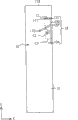
请参见图1,本发明的天线1设置在一可携式电子装置(移动电话)3的壳体31中,壳体31包括一显示单元32,而天线1即设置在显示单元32的一侧,另外,在壳体中还设置有另一天线2,位于显示单元32的上侧。在上述中,天线1为WiFi天线,而天线2则用以接收卫星信号。Please refer to Fig. 1,
再请参见图2,说明本发明的天线1。本发明的天线1主要包括一基板11、一接地组件12、一传输组件13以及一缆线15。接地组件12设置在基板11的一第一面S1上,并具有一大体为矩形的开槽C,开槽C的开口朝向接地组件12的一侧边121,且开槽C具有一第一侧C1、一第二侧C2及一第三侧C3,第二侧C2连接且垂直于第一侧C1及第三侧C3。传输组件13设置在基板11的一第二面S2,并且与接地组件12电性连接。缆线15由第二面S2与传输组件13连接,借以传输无线信号。当传输组件13投影在第一面S1时,传输组件13在第一面S1的投影大体上对应于开槽C且与开槽C部份重迭。Referring to FIG. 2 again, the
传输组件13包括一接地部131、一互连部132、一馈入部133以及一延伸部134,接地部131是与接地组件12连接,馈入部133是与缆线15连接,而互连部132则连接接地部131、馈入部133及延伸部134。在互连部132及馈入部133之间具有一夹角θ1,夹角θ1介于0度至180度之间。The
接着,请配合参见图2及图3,如图所示,接地部131的位置大致对应于开槽C的第一侧C1的位置,互连部132的位置大致对应于开槽C的开口的位置,馈入部133跨越开槽C的第二侧C2,而延伸部134的位置大致对应于开槽C的第三侧C3的位置。更详细地说,接地部131平行于开槽C的第一侧C1,且接地部131在第一面S1的投影正好位于开槽C的第一侧C1上,互连部132平行且邻近于接地板12的侧边121,而延伸部134平行于开槽C的第三侧C3,且延伸部134在第一面S1的投影邻近于开槽C的第三侧C3。上述的传输组件13的接地部131、互连部132、馈入部133及延伸部134大体上对应于开槽C而排列成E型。Next, please refer to FIG. 2 and FIG. 3 , as shown in the figure, the position of the
在本实施例中,开槽C的第一侧C1与基板的一侧边113相距一距离G,此距离G至少为1毫米。另外,开槽C的第二侧C2是与接地组件12的一侧边121’平行,侧边121’的长度约为第二侧C2的长度的五倍。并且,接地部131的长度大致等于第一侧C1的长度,即,传输组件13的接地部131与接地组件12电性连接的位置恰好位于开槽C的角落上。同时,互连部132及馈入部133之间的夹角θ1为90度。In this embodiment, the distance G between the first side C1 of the slot C and one
另外,基于配线的原因,亦可在基板11上开设有贯穿孔111及孔洞112,传输组件13的接地部131经由贯穿孔111而与基板11的第一面S1的接地组件12连接,而缆线则由基板11的第一面S1透过孔洞112而与传输组件13的馈入部133连接。In addition, for wiring reasons, the
由于本发明的天线1将接地组件12当作天线的辐射体,故可大幅减小整体的体积,另外,当天线1设置在电子装置3中时,邻近于天线1的电子装置3的金属壳体3 1或电子装置3中的其它金属组件,均可与天线1配合,作为天线1的辐射体,因此,本发明的天线1可视之为多辐射体天线,因而增加了天线1的频宽。请搭配参阅图4,电压驻波比(VSWR)小于2的频宽约为700~800MHz,也就是说,本发明的天线1不易因身体遮蔽效应而让天线1产生频偏而失效。Since the
以下将以第2及3图所示的天线1为基础,各别说明本发明的天线1的数个变化例,相同的部份将不再赘述。需注意的是,下述的变化例可交错搭配使用,以使本发明的天线1具有最优的信号传输效果。Based on the
请参见图5,显示本发明天线1的接地部131’的一个变化例。其中,接地部131’平行于开槽C的第一侧C1,且接地部131’在第一面S1的投影邻近于开槽C的第一侧C1,更详细地说,接地部131’在第一面S1的投影位于开槽C的第一侧C1的上方,两者相隔一间距。Please refer to FIG. 5 , which shows a variation example of the ground portion 131' of the
再请参见图6,显示本发明天线1的接地部131”的另一个变化例。其中,接地部131”平行于开槽C的第一侧C1,且接地部131”在第一面S1的投影邻近于开槽C的第一侧C1,更详细地说,接地部131”在第一面S1的投影位于开槽C的第一侧C1的下方,两者相隔一间距。Referring to FIG. 6 again, it shows another variation example of the
再请参见图7,显示本发明天线1的接地部131的又一个变化例。其中,接地部131

请参见图8,显示本发明天线1的互连部132’的一个变化例。其中,互连部132’对应于开槽C的开口且平行于接地板12的侧边121,更详细地说,互连部132’位于侧边121左侧,两者相隔一间距。Please refer to FIG. 8 , which shows a modification example of the interconnection portion 132' of the
再请参见图9,显示本发明天线1的互连部132”的另一个变化例。其中,互连部1 32”对应于开槽C的开口且大体上平行于接地板12的侧边121,互连部132”包括一变形部D,变形部D与互连部132”具有不同的外型。例如图9上所示,变形部D在第一轴(X轴)上的宽度大于互连部132”在第一轴(X轴)上的宽度。Referring to Fig. 9 again, it shows another modification example of the
再请参见图10,显示本发明天线1的互连部132
请参见图11,显示本发明天线1的馈入部133’的一个变化例。其中,馈入部133’跨越开槽C的第二侧C2,且互连部132及馈入部133’之间的夹角θ1小于90度。Please refer to FIG. 11 , which shows a modification example of the feeding part 133' of the
再请参见图12,显示本发明天线1的馈入部133”的另一个变化例。其中,馈入部133”包括一第一段部133a及一第二段部133b,第一段部133a与互连部132连接,第二段部133b与缆线15连接,在第一段部133a与第二段部133b之间夹有一角度θ2,角度θ2介于0度至180度之间。例如图12上所示,角度θ2大于90度。Referring to Fig. 12 again, it shows another variation example of the feed-in
请参见图13,显示本发明天线1的延伸部134’的一个变化例。其中,延伸部134’平行于开槽C的第三侧C3,且延伸部134’在第一面S1的投影邻近于开槽C的第三侧C3,更详细地说,延伸部134’在第一面S1的投影位于开槽C的第三侧C3的上方,两者相隔一间距。Please refer to FIG. 13 , which shows a modification example of the extension portion 134' of the
请参见图14,在本实施例中,传输组件13包括接地部131、互连部132以及馈入部133,不具有延伸部134,或者,可以将延伸部134视为与互连部132平行,而连结成一体。另外,传输组件13的接地部131、互连部132及馈入部133大体上对应于开槽C而排列成F型。Referring to FIG. 14 , in this embodiment, the
请参见图15,显示本发明天线1的接地组件12’的一个变化例。其中,接地组件12’的外型大体为矩形并具有开槽C,且接地组件12’上还具有至少一穿孔123,贯穿接地组件12’的两侧面。或者,例如图15上所示,接地组件12’上具有多个穿孔123,大致上呈矩阵排列。Please refer to FIG. 15 , which shows a modification example of the ground component 12' of the
再请参见图16,显示本发明天线1的接地组件12”的另一个变化例。其中,接地组件12”的外型大体为矩形并具有开槽C,且接地组件12”还具有一锯齿型结构124。Referring to Fig. 16 again, it shows another variation example of the
再请参见图17,显示本发明天线1的接地组件12

另外,需说明的是,本发明的天线的使用频率约在2.4GHz至2.5GHz之间,当人体靠近本发明的天线时,请参见图18,输入回波耗损(Input ReturnLoss)低于-10dB的范围在2.1GHz至2.53GHz之间,故本发明的天线能确保频率2.4GHz至2.5GHz之间为有效的传输信号频宽。In addition, it should be noted that the operating frequency of the antenna of the present invention is between 2.4GHz and 2.5GHz. When the human body is close to the antenna of the present invention, please refer to Figure 18, and the input return loss (Input ReturnLoss) is lower than -10dB The frequency range is between 2.1 GHz and 2.53 GHz, so the antenna of the present invention can ensure an effective transmission signal bandwidth between 2.4 GHz and 2.5 GHz.
以上所述仅为本发明的优选实施例,凡依本发明所做的均等变化与修饰,均应属本发明的涵盖范围。The above descriptions are only preferred embodiments of the present invention, and all equivalent changes and modifications made according to the present invention shall fall within the scope of the present invention.
Claims (29)
Priority Applications (1)
| Application Number | Priority Date | Filing Date | Title |
|---|---|---|---|
| CN2006100748963A CN101064379B (en) | 2006-04-25 | 2006-04-25 | Portable electronic device and its antenna |
Applications Claiming Priority (1)
| Application Number | Priority Date | Filing Date | Title |
|---|---|---|---|
| CN2006100748963A CN101064379B (en) | 2006-04-25 | 2006-04-25 | Portable electronic device and its antenna |
Publications (2)
| Publication Number | Publication Date |
|---|---|
| CN101064379A CN101064379A (en) | 2007-10-31 |
| CN101064379B true CN101064379B (en) | 2011-06-15 |
Family
ID=38965210
Family Applications (1)
| Application Number | Title | Priority Date | Filing Date |
|---|---|---|---|
| CN2006100748963A Active CN101064379B (en) | 2006-04-25 | 2006-04-25 | Portable electronic device and its antenna |
Country Status (1)
| Country | Link |
|---|---|
| CN (1) | CN101064379B (en) |
Families Citing this family (5)
| Publication number | Priority date | Publication date | Assignee | Title |
|---|---|---|---|---|
| CN102244313A (en) * | 2010-05-13 | 2011-11-16 | 广达电脑股份有限公司 | Antenna device with slot structure |
| CN103036583A (en) * | 2011-10-08 | 2013-04-10 | 宏碁股份有限公司 | Communication electronic device and antenna structure thereof |
| US11050150B2 (en) | 2017-12-01 | 2021-06-29 | Samsung Electro-Mechanics Co., Ltd. | Antenna apparatus and antenna module |
| CN109873247B (en) * | 2017-12-01 | 2021-06-18 | 三星电机株式会社 | Antenna device and antenna module |
| US10978796B2 (en) | 2017-12-28 | 2021-04-13 | Samsung Electro-Mechanics Co., Ltd. | Antenna apparatus and antenna module |
Citations (2)
| Publication number | Priority date | Publication date | Assignee | Title |
|---|---|---|---|---|
| US6359589B1 (en) * | 2000-06-23 | 2002-03-19 | Kosan Information And Technologies Co., Ltd. | Microstrip antenna |
| US6825811B2 (en) * | 2001-08-09 | 2004-11-30 | Matsushita Electric Industrial Co., Ltd. | Display-antenna integral structure and communication apparatus |
-
2006
- 2006-04-25 CN CN2006100748963A patent/CN101064379B/en active Active
Patent Citations (2)
| Publication number | Priority date | Publication date | Assignee | Title |
|---|---|---|---|---|
| US6359589B1 (en) * | 2000-06-23 | 2002-03-19 | Kosan Information And Technologies Co., Ltd. | Microstrip antenna |
| US6825811B2 (en) * | 2001-08-09 | 2004-11-30 | Matsushita Electric Industrial Co., Ltd. | Display-antenna integral structure and communication apparatus |
Also Published As
| Publication number | Publication date |
|---|---|
| CN101064379A (en) | 2007-10-31 |
Similar Documents
| Publication | Publication Date | Title |
|---|---|---|
| US7385556B2 (en) | Planar antenna | |
| US7053844B2 (en) | Integrated multiband antennas for computing devices | |
| TWI686996B (en) | Antenna structure | |
| TWI646730B (en) | Mobile device | |
| TWI672863B (en) | Antenna structure | |
| US7554488B2 (en) | Planar antenna | |
| CN101507044A (en) | Conformal and compact wideband antenna | |
| TWI715316B (en) | Antenna structure | |
| US9368858B2 (en) | Internal LC antenna for wireless communication device | |
| CN101064379B (en) | Portable electronic device and its antenna | |
| US20090179800A1 (en) | Antenna structure | |
| CN112864608A (en) | Antenna structure | |
| CN112886194A (en) | Antenna structure | |
| TWI802157B (en) | Antenna structure | |
| CN112701453A (en) | Antenna structure | |
| TWI699043B (en) | Antenna structure | |
| CN101217214B (en) | Three-dimensional broadband antenna and related wireless communication device | |
| CN101207236B (en) | Multi-frequency antenna | |
| US7312755B2 (en) | Internal antenna of wireless communication terminal | |
| US9431710B2 (en) | Printed wide band monopole antenna module | |
| US7315284B2 (en) | Portable device and antenna thereof | |
| CN111725609B (en) | Antenna structure | |
| TWI553962B (en) | Multimode monopole antenna | |
| US7541980B2 (en) | Printed antenna | |
| CN115249891A (en) | Antenna structure |
Legal Events
| Date | Code | Title | Description |
|---|---|---|---|
| C06 | Publication | ||
| PB01 | Publication | ||
| C10 | Entry into substantive examination | ||
| SE01 | Entry into force of request for substantive examination | ||
| C14 | Grant of patent or utility model | ||
| GR01 | Patent grant |