CN101030556A - Method of manufacturing a semiconductor device - Google Patents
Method of manufacturing a semiconductor device Download PDFInfo
- Publication number
- CN101030556A CN101030556A CNA2007100072315A CN200710007231A CN101030556A CN 101030556 A CN101030556 A CN 101030556A CN A2007100072315 A CNA2007100072315 A CN A2007100072315A CN 200710007231 A CN200710007231 A CN 200710007231A CN 101030556 A CN101030556 A CN 101030556A
- Authority
- CN
- China
- Prior art keywords
- film
- misfet
- gate electrode
- insulating film
- formation region
- Prior art date
- Legal status (The legal status is an assumption and is not a legal conclusion. Google has not performed a legal analysis and makes no representation as to the accuracy of the status listed.)
- Granted
Links
Images


Classifications
-
- H—ELECTRICITY
- H10—SEMICONDUCTOR DEVICES; ELECTRIC SOLID-STATE DEVICES NOT OTHERWISE PROVIDED FOR
- H10B—ELECTRONIC MEMORY DEVICES
- H10B43/00—EEPROM devices comprising charge-trapping gate insulators
- H10B43/30—EEPROM devices comprising charge-trapping gate insulators characterised by the memory core region
-
- H—ELECTRICITY
- H10—SEMICONDUCTOR DEVICES; ELECTRIC SOLID-STATE DEVICES NOT OTHERWISE PROVIDED FOR
- H10B—ELECTRONIC MEMORY DEVICES
- H10B43/00—EEPROM devices comprising charge-trapping gate insulators
- H10B43/40—EEPROM devices comprising charge-trapping gate insulators characterised by the peripheral circuit region
-
- H—ELECTRICITY
- H10—SEMICONDUCTOR DEVICES; ELECTRIC SOLID-STATE DEVICES NOT OTHERWISE PROVIDED FOR
- H10D—INORGANIC ELECTRIC SEMICONDUCTOR DEVICES
- H10D84/00—Integrated devices formed in or on semiconductor substrates that comprise only semiconducting layers, e.g. on Si wafers or on GaAs-on-Si wafers
- H10D84/01—Manufacture or treatment
- H10D84/0123—Integrating together multiple components covered by H10D12/00 or H10D30/00, e.g. integrating multiple IGBTs
- H10D84/0126—Integrating together multiple components covered by H10D12/00 or H10D30/00, e.g. integrating multiple IGBTs the components including insulated gates, e.g. IGFETs
- H10D84/0144—Manufacturing their gate insulating layers
-
- H—ELECTRICITY
- H10—SEMICONDUCTOR DEVICES; ELECTRIC SOLID-STATE DEVICES NOT OTHERWISE PROVIDED FOR
- H10D—INORGANIC ELECTRIC SEMICONDUCTOR DEVICES
- H10D84/00—Integrated devices formed in or on semiconductor substrates that comprise only semiconducting layers, e.g. on Si wafers or on GaAs-on-Si wafers
- H10D84/01—Manufacture or treatment
- H10D84/02—Manufacture or treatment characterised by using material-based technologies
- H10D84/03—Manufacture or treatment characterised by using material-based technologies using Group IV technology, e.g. silicon technology or silicon-carbide [SiC] technology
- H10D84/038—Manufacture or treatment characterised by using material-based technologies using Group IV technology, e.g. silicon technology or silicon-carbide [SiC] technology using silicon technology, e.g. SiGe
-
- H—ELECTRICITY
- H10—SEMICONDUCTOR DEVICES; ELECTRIC SOLID-STATE DEVICES NOT OTHERWISE PROVIDED FOR
- H10D—INORGANIC ELECTRIC SEMICONDUCTOR DEVICES
- H10D84/00—Integrated devices formed in or on semiconductor substrates that comprise only semiconducting layers, e.g. on Si wafers or on GaAs-on-Si wafers
- H10D84/80—Integrated devices formed in or on semiconductor substrates that comprise only semiconducting layers, e.g. on Si wafers or on GaAs-on-Si wafers characterised by the integration of at least one component covered by groups H10D12/00 or H10D30/00, e.g. integration of IGFETs
- H10D84/811—Combinations of field-effect devices and one or more diodes, capacitors or resistors
- H10D84/813—Combinations of field-effect devices and capacitor only
Landscapes
- Non-Volatile Memory (AREA)
- Metal-Oxide And Bipolar Metal-Oxide Semiconductor Integrated Circuits (AREA)
- Electrodes Of Semiconductors (AREA)
- Semiconductor Memories (AREA)
Abstract
本发明提供了一种半导体器件的制造方法,这种制造方法包括:在半导体衬底之上形成栅极绝缘膜、电荷存储膜、绝缘膜、多晶硅膜、氧化硅膜、氮化硅膜和盖层绝缘膜的膜层叠;通过光刻和蚀刻从低击穿电压MISFET形成区和高击穿电压MISFET形成区中清除所述膜层叠;在所述半导体衬底之上形成栅极绝缘膜、多晶硅膜和盖层绝缘膜,在低击穿电压MISFET形成区和高击穿电压MISFET形成区中形成栅电极,然后在存储器单元形成区中形成栅电极。通过这种在不同的步骤中形成第一MISFET和第二MISFET的栅电极的半导体器件的制造技术,本发明能够提供每个具有改进的可靠性的第一MISFET和第二MISFET。
The present invention provides a manufacturing method of a semiconductor device, which includes: forming a gate insulating film, a charge storage film, an insulating film, a polysilicon film, a silicon oxide film, a silicon nitride film and a capping film over a semiconductor substrate. film lamination of a layer insulating film; removing said film lamination from a low breakdown voltage MISFET formation region and a high breakdown voltage MISFET formation region by photolithography and etching; forming a gate insulating film, polysilicon over said semiconductor substrate film and a cap insulating film, a gate electrode is formed in a low breakdown voltage MISFET formation region and a high breakdown voltage MISFET formation region, and then a gate electrode is formed in a memory cell formation region. Through such a manufacturing technique of a semiconductor device in which the gate electrodes of the first MISFET and the second MISFET are formed in different steps, the present invention can provide the first MISFET and the second MISFET each having improved reliability.
Description
相关申请的交叉引用Cross References to Related Applications
本申请要求2006年3月1日申请的日本专利申请第2006-54637号的优先权利益,在此以引用参考的方式将其内容并入在本申请中。This application claims the benefit of priority from Japanese Patent Application No. 2006-54637 filed on March 1, 2006, the contents of which are hereby incorporated by reference into this application.
技术领域technical field
本发明涉及一种半导体器件的制造技术,具体地说,涉及一种在用于通过不同的步骤制造第一MISFET的栅极电极和第二MISFET的栅极电极时有效的技术。The present invention relates to a manufacturing technique of a semiconductor device, and in particular, to a technique effective when used to manufacture a gate electrode of a first MISFET and a gate electrode of a second MISFET through different steps.
背景技术Background technique
在日本未审查的专利出版物第2004-40041号中,公开了一种在一个半导体衬底上形成在低压下工作的低压晶体管和在高压下工作的闪速存储器两者并且具有被称为ETOX的双层电极结构的技术。In Japanese Unexamined Patent Publication No. 2004-40041, it is disclosed that both a low-voltage transistor operating at a low voltage and a flash memory operating at a high voltage are formed on one semiconductor substrate and have a so-called ETOX The technology of double-layer electrode structure.
具体地,描述了用于元件隔离的场氧化物膜和用于离子注入的保护氧化物膜都被形成在半导体衬底上以便形成低压晶体管区和闪速存储器区。在通过光刻法形成其中仅仅开有(open)低压晶体管区的第一抗蚀剂图形之后,实施用于控制低压晶体管的阈值电压的离子注入。清除第一抗蚀剂图形,然后再次执行光刻法以形成其中仅开有闪速存储器区的第二抗蚀剂图形。通过蚀刻仅仅从闪速存储器区中清除保护氧化物膜。Specifically, it is described that a field oxide film for element isolation and a protective oxide film for ion implantation are both formed on a semiconductor substrate to form a low-voltage transistor region and a flash memory region. After forming the first resist pattern in which only the low voltage transistor region is opened by photolithography, ion implantation for controlling the threshold voltage of the low voltage transistor is performed. The first resist pattern is erased, and then photolithography is performed again to form a second resist pattern in which only the flash memory area is opened. The protective oxide film is removed only from the flash memory area by etching.
在清除了第二抗蚀剂图形之后,形成闪速存储器的栅极氧化物膜,然后在闪速存储器区之上形成第一级栅极电极材料。通过蚀刻从低压晶体管区中清除保护氧化物膜,由此形成低压晶体管的栅极氧化物膜。与此同时,形成闪速存储器的层间绝缘膜。在形成了第二级栅极电极材料之后,执行光刻和蚀刻以形成闪速存储器的栅极电极和低压晶体管的栅极电极。After the second resist pattern is removed, a gate oxide film of the flash memory is formed, and then a first-level gate electrode material is formed over the flash memory region. The protective oxide film is removed from the low-voltage transistor region by etching, thereby forming a gate oxide film of the low-voltage transistor. At the same time, an interlayer insulating film of the flash memory is formed. After the second-level gate electrode material is formed, photolithography and etching are performed to form the gate electrode of the flash memory and the gate electrode of the low voltage transistor.
电可编程的非易失性半导体存储器件(半导体器件)可以执行机载程序重写由此可以缩短程序开发周期并提高开发效率。此外,存储器件将其应用例如扩展到高混合的低产量生产和用于每个目的的调谐。具体地,近年来,对于其上安装有EEPROM(电可擦除的可编程的只读存储器)的微型计算机的需求日益增加。An electrically programmable nonvolatile semiconductor memory device (semiconductor device) can perform on-board program rewriting and thus can shorten a program development cycle and improve development efficiency. In addition, memory devices expand their applications, for example, to high-mix low-volume production and tuning for each purpose. Specifically, in recent years, there has been an increasing demand for a microcomputer on which an EEPROM (Electrically Erasable Programmable Read Only Memory) is mounted.
作为电可编程的非易失性半导体存储器件,主要使用具有多晶硅膜作为电荷存储膜的EEPROM。As an electrically programmable nonvolatile semiconductor memory device, an EEPROM having a polysilicon film as a charge storage film is mainly used.
然而,具有多晶硅膜作为电荷存储膜的EEPROM具有的问题是:由于电荷存储膜是导体,因此仅在包含多晶硅膜的一部分氧化物膜中的缺陷导致了异常泄漏,并且在电荷存储膜中累积的所有电子从电荷存储膜中逃逸。具体地说,随着将来尺寸的进一步减小和集成度的增加,上述问题变得更加突出。However, an EEPROM having a polysilicon film as a charge storage film has a problem that, since the charge storage film is a conductor, defects in only a part of the oxide film including the polysilicon film cause abnormal leakage, and the accumulated in the charge storage film All electrons escape from the charge storage membrane. Specifically, the above-mentioned problems will become more prominent with further reduction in size and increase in integration in the future.
人们提出了不使用多晶硅膜而是使用氮化硅膜(Si3N4)作为电荷存储膜的MNOS(金属氮化物氧化物半导体)结构和MONOS(金属氧化物氮化物氧化物半导体)结构。在这种情况下,电子存储在用作绝缘体的氮化物膜的离散俘获电平中,因此即使在一部分电荷存储膜中产生了缺陷和发生了异常泄漏,在电荷存储膜中存储的所有电子都不逃逸。因此,可以改善数据保持的可靠性。An MNOS (Metal Nitride Oxide Semiconductor) structure and a MONOS (Metal Oxide Nitride Oxide Semiconductor) structure using not a polysilicon film but a silicon nitride film (Si 3 N 4 ) as a charge storage film have been proposed. In this case, electrons are stored in discrete trapping levels of the nitride film serving as an insulator, so even if defects are generated in a part of the charge storage film and abnormal leakage occurs, all electrons stored in the charge storage film are lost. Do not escape. Therefore, the reliability of data retention can be improved.
如上文所述的非易失性半导体存储器件配备有存储器单元阵列和用于驱动这个存储器单元阵列的外围电路,在这种存储器单元阵列中二维地设置了具有MONOS结构的多个存储器单元。外围电路包括具有相对较高的击穿电压的高击穿电压MISFET(金属绝缘体半导体场效应晶体管)和具有相对较低的击穿电压的低击穿电压MISFET。高击穿电压MISFET被用作解码器或者升压电路。这些存储器单元、高击穿电压MISFET和低击穿电压MISFET都形成在一个半导体衬底上。换句话说,构成存储器单元的MONOS晶体管(一种MISFET)和构成外围电路的MISFET都形成在一个半导体衬底上。在形成它们时,MONOS晶体管的栅极电极和用于外围电路的MISFET的栅极电极都在不同的步骤中形成。接着参考一些附图描述形成构成存储器单元的MONOS晶体管的栅极电极和构成外围电路的MISFET的栅极电极的步骤。低击穿电压MISFET和高击穿电压MISFET构成了外围电路,但是在下文用于描述的附图中,低击穿电压MISFET被作为构成外围电路的MISFET的实例给出。The nonvolatile semiconductor memory device as described above is equipped with a memory cell array in which a plurality of memory cells having a MONOS structure are arranged two-dimensionally and a peripheral circuit for driving this memory cell array. The peripheral circuit includes a high breakdown voltage MISFET (Metal Insulator Semiconductor Field Effect Transistor) having a relatively high breakdown voltage and a low breakdown voltage MISFET having a relatively low breakdown voltage. A high breakdown voltage MISFET is used as a decoder or boost circuit. These memory cells, high breakdown voltage MISFETs and low breakdown voltage MISFETs are all formed on one semiconductor substrate. In other words, MONOS transistors (a kind of MISFET) constituting memory cells and MISFETs constituting peripheral circuits are formed on one semiconductor substrate. When forming them, the gate electrode of the MONOS transistor and the gate electrode of the MISFET used for peripheral circuits are formed in different steps. Next, steps of forming gate electrodes of MONOS transistors constituting memory cells and gate electrodes of MISFETs constituting peripheral circuits will be described with reference to some of the drawings. The low breakdown voltage MISFET and the high breakdown voltage MISFET constitute a peripheral circuit, but in the drawings used for description below, a low breakdown voltage MISFET is given as an example of the MISFET constituting the peripheral circuit.
存在两种技术。第一种技术是形成MONOS晶体管的栅极电极,然后形成构成外围电路的MISFET的栅极电极。There are two techniques. The first technique is to form the gate electrode of the MONOS transistor, and then form the gate electrode of the MISFET constituting the peripheral circuit.
如附图38所示,通过热氧化在包括存储器单元法形成区和外围电路形成区的半导体衬底200之上形成栅极绝缘膜201。例如通过CVD(化学汽相淀积)在栅极绝缘膜201之上形成电荷存储膜202。然后例如通过CVD形成电位阻挡膜203,之后例如通过CVD在电位阻挡膜203上形成多晶硅膜204。栅极绝缘膜201和电位阻挡膜203例如由硅氧化物膜形成,同时电荷存储膜202例如由氮化硅膜形成。As shown in FIG. 38, a
如附图39所示,通过光刻和蚀刻在存储器单元形成区中形成MONOS晶体管的栅极电极205。这时,栅极绝缘膜(第一电位阻挡膜)201、电荷存储膜202和电位阻挡膜(第二电位阻挡膜)203都已经被形成在栅极电极205和半导体衬底200之间。如附图40所示,然后例如通过热氧化在具有栅极电极205的半导体衬底200上形成栅极绝缘膜206,然后在栅极绝缘膜206之上形成多晶硅膜207。As shown in FIG. 39, the
多晶硅膜207和栅极绝缘膜206由光刻处理,并蚀刻以在如附图41所示的外围电路形成区中形成MISFET的栅极电极208。在栅极电极208和半导体衬底200之间,形成栅极绝缘膜206。如附图41所示,蚀刻残余209仍然保留在MONOS晶体管的栅极电极205的侧壁上。The
如附图42所示,形成了抗蚀剂图形210。对抗蚀剂图形210进行构图以覆盖外围电路形成区并暴露了存储器单元形成区。通过以抗蚀剂图形210作为掩模进行蚀刻,清除在栅极电极205的侧壁上形成的蚀刻残余209。如附图43所示,通过清除抗蚀剂图形210,在存储器单元形成区中可以形成MONOS晶体管的栅极电极205,并在外围电路形成区中可以形成MISFET的栅极电极208。As shown in Fig. 42, a
然而,第一种技术具有如下的问题。如附图40所示,在存储器单元形成区中MONOS晶体管的栅极电极205的形成之后,在半导体衬底200的整个表面之上形成栅极绝缘膜206。通过这个步骤,氧化了构成栅极电极205的多晶硅膜。特别是在栅极电极205的侧壁的端部部分(它是与电位阻挡膜203相邻的边界附近的区域)上发生了氧化,并在栅极电极205的端部部分上形成鸟嘴(bird’s beak)。另一鸟嘴出现在半导体衬底200与栅极绝缘膜201相接触的位置上,它增加了栅极绝缘膜201在端部部分上的厚度。在电子注入到电荷存储膜202或者从其中射出时栅极绝缘膜201用作隧道绝缘膜。因此通过形成鸟嘴使栅极绝缘膜201加厚干扰了隧道现象的发生,使得难以将电子注入到电荷存储膜202中或从其中射出。这延迟了数据写入或擦除,最后劣化了MONOS晶体管的特性。例如,在鸟嘴出现在栅极绝缘膜201(它将是隧道绝缘膜)中时,栅极绝缘膜201将在已出现鸟嘴的区域中变厚,这影响了数据的平稳擦除。然后,通过擦除操作,阈值电压不会降低到预定的电平,并且读电流通过重写的重复而降低。除了这个问题之外,在小型化栅极电极205时,在栅极电极205中的鸟嘴区的百分比增加,由此降低了栅极绝缘膜201的厚度的可控性。这导致了读电流的降低或者短沟道特性的劣化。However, the first technique has problems as follows. As shown in FIG. 40 , after the formation of the
在第一种技术中,如附图41所示,蚀刻残余209仍然保留在栅极电极205的侧壁上,因此蚀刻残余209必须被清除。例如通过干蚀刻清除蚀刻残余209,但恐怕这种干蚀刻在栅极电极205的端部部分上造成蚀刻损坏。为了减轻蚀刻损坏,需要用于事先氧化栅极电极205的表面的轻度氧化步骤,并且这有利于在栅极绝缘膜201的端部部分上形成鸟嘴。In the first technique, as shown in FIG. 41, the
在构成外围电路的MISFET的栅极电极208的形成之前形成MONOS晶体管的栅极电极205时,因此发生了上述问题。第二种技术是形成构成外围电路的MISFET的栅极电极之后形成MONOS晶体管的栅极电极的技术。下文参考一些附图描述这种技术。When the
如附图44所述,通过例如热氧化作用在包括存储器单元形成区和外围电路形成区的半导体衬底300上形成由氧化硅膜形成的栅极绝缘膜301。例如通过CVD(化学汽相淀积)在栅极绝缘膜301上形成多晶硅膜302。As shown in FIG. 44, a
如附图45所示,多晶硅膜302通过光刻和蚀刻处理以在外围电路形成区中形成栅极电极303。As shown in FIG. 45, the
如附图46所示,栅极绝缘膜304、电荷存储膜305和电位阻挡膜306都形成在其上形成有栅极电极303的半导体衬底300的整个表面上。然后在电位阻挡膜306上形成多晶硅膜307。如附图47所示,通过光刻和蚀刻在存储器单元形成区中形成栅极电极308。这时,蚀刻残余309保留在外围电路形成区中形成的栅极电极303的侧壁上。As shown in FIG. 46, a
如附图48所示,形成抗蚀剂图形310。这种抗蚀剂图形310被构图以覆盖存储器单元形成区并暴露外围电路形成区。通过使用这种抗蚀剂图形310作为掩模进行蚀刻,清除在栅极电极303的侧壁上形成的蚀刻残余309。如附图49所示,清除抗蚀剂图形310,由此在存储器单元形成区中形成栅极电极308,同时在外围电路形成区中形成栅极电极303。As shown in FIG. 48, a resist
根据这第二种技术,在外围电路的MISFET的栅极电极303之后形成MONOS晶体管的栅极电极308。在用于外围电路的栅极绝缘膜301形成期间,MONOS晶体管的栅极绝缘膜304因此不被氧化并且在MONOS晶体管中不会出现鸟嘴。According to this second technique, the
然而,在MONOS晶体管的栅极电极308之前的外围电路的MISFET的栅极电极308的形成会造成如下问题。However, the formation of the
如附图46所示,在外围电路形成区中的MISFET的栅极电极303的形成之后,在半导体衬底300的整个表面上形成栅极绝缘膜304。在栅极绝缘膜304的形成期间,栅极电极303的端部部分被氧化并且在栅极绝缘膜301的端部部分上出现鸟嘴。在栅极绝缘膜301的端部部分处的鸟嘴的形成增加了栅极绝缘膜301在其端部部分上的厚度。在其端部部分上的栅极绝缘膜301的厚度的增加降低了在外围电路的MISFET的源极区和漏极区之间流动的电流。总之,这种电流的幅度与栅极绝缘膜301的厚度成反比。在栅极绝缘膜301变厚时,在源极和漏极区之间流动的电流不能被固定,并且外围电路的MISFET的特性劣化。此外,在使外围电路的MISFET(具体地,低击穿电压MISFET)小型化时,栅极电极303的栅极长度变短,导致阈值电压降低的短沟道特性变得突出。随着栅极绝缘膜30变得越薄,短沟道特性得到了改善。然而,在通过鸟嘴的形成增加了栅极绝缘膜301的厚度时,短沟道特性变得更加突出,外围电路的MISFET的特性被劣化了。As shown in FIG. 46 , after the formation of the
在第二种技术中,如附图47所示,蚀刻残余309保留在栅极电极303的侧壁上因此这种蚀刻残余309必须被清除。例如通过干蚀刻清除蚀刻残余309。然而这种干蚀刻可能在栅极电极309的端部部分处造成蚀刻损坏。In the second technique, as shown in FIG. 47, etch residue 309 remains on the sidewall of the
此外,在第二种技术中,如附图45所示,大约3纳米的氧化硅被用作外围电路的MISFET(低击穿电压MISFET)的栅极绝缘膜301。在外围电路形成区(低击穿电压MISFET形成区)中,在通过处理形成了栅极电极303之后,仅仅是具有小于3纳米厚的氧化硅保留下来(在附图45中没有示出)。如附图47所示,在通过处理形成MONOS晶体管的栅极电极308时清除在外围电路形成区中保留的多晶硅膜307、电位阻挡膜306、电荷存储膜305和栅极绝缘膜304。在清除了由氮化硅膜形成的这种电荷存储膜305时,在电荷存储膜305之下存在的氧化硅膜(小于3纳米厚的氧化硅膜和栅极绝缘膜304的组合)如此薄以至使栅极电极303的边缘被暴露于用于清除氮化硅膜的热磷酸中。这可能导致由于半导体衬底300的不理想的蚀刻引起的栅极缺陷的密度和故障的增加。Furthermore, in the second technique, as shown in FIG. 45, silicon oxide of about 3 nanometers is used as the
如上文所述,即使利用第一种技术或者第二种技术中的任一种技术,在两个电极之间首先形成的栅极电极不可避免地存在问题。As described above, even with either of the first technique or the second technique, there is inevitably a problem with the gate electrode formed first between the two electrodes.
发明内容Contents of the invention
本发明的一个目的是一种在半导体器件的制造技术中提供一种能够改善第一MISFET和第二MISFET中的每一个的可靠性的技术,这种制造技术包含在不同的步骤中形成第一MISFET的栅极电极和第二MIEFET的栅极电极。An object of the present invention is to provide a technique capable of improving the reliability of each of a first MISFET and a second MISFET in a manufacturing technique of a semiconductor device that includes forming the first MISFET in different steps. the gate electrode of the MISFET and the gate electrode of the second MIEFET.
通过在此的描述和附图将会清楚本发明的上述和其它目的和新颖特征。The above and other objects and novel features of the present invention will be apparent from the description herein and the accompanying drawings.
下文将简要地描述本申请所公开的典型的发明概要。The following will briefly describe the outline of typical inventions disclosed in the present application.
本发明属于这样的一种半导体器件的制造方法:在半导体衬底的第一区上形成第一MISFET和在半导体衬底的第二区上形成第二MISFET。该方法包括如下步骤:(a)在包括第一区和第二区的半导体衬底上形成第一绝缘膜,(b)在第一绝缘膜上形成第一导体膜,和(c)清除在第二区上形成的第一绝缘膜和第一导体膜。该方法进一步包括如下步骤:(d)在步骤(c)之后,在包括第二区的半导体衬底和包括第一区的第一导体膜上形成第二绝缘膜,(e)在第二绝缘膜上形成第二导体膜,和(f)对第二导体膜和第二绝缘膜进行构图以在第二区中形成第二MISFET的第二栅极电极。该方法进一步包括如下步骤:(g)在步骤(f)之后,对在第一区中形成的第一导体膜和第一绝缘膜进行构图以在第一区中形成第一MISFET的第一栅极电极。The present invention pertains to a method of manufacturing a semiconductor device in which a first MISFET is formed on a first region of a semiconductor substrate and a second MISFET is formed on a second region of the semiconductor substrate. The method includes the steps of: (a) forming a first insulating film on a semiconductor substrate including a first region and a second region, (b) forming a first conductor film on the first insulating film, and (c) cleaning the The first insulating film and the first conductor film are formed on the second region. The method further includes the steps of: (d) after step (c), forming a second insulating film on the semiconductor substrate including the second region and the first conductor film including the first region, (e) forming a second insulating film on the second insulating film forming a second conductor film on the film, and (f) patterning the second conductor film and the second insulating film to form a second gate electrode of the second MISFET in the second region. The method further includes the step of: (g) after step (f), patterning the first conductor film and the first insulating film formed in the first region to form the first gate of the first MISFET in the first region pole electrode.
下文接着描述本申请所公开的通过典型的发明可获得的优点。Advantages obtainable by typical inventions disclosed in the present application are described next below.
在通过处理形成第一MISFET的第一栅极电极和第二MISFET的第二栅极电极之前,形成用于第一栅极电极和第二栅极电极的形成的相应的导体膜。在形成了这些导体膜之后,实施第一栅极电极和第二栅极电极的形成的处理以使得可以改善第一MISFET和第二MISFET的可靠性。Before the first gate electrode of the first MISFET and the second gate electrode of the second MISFET are formed by processing, respective conductor films for the formation of the first gate electrode and the second gate electrode are formed. After these conductor films are formed, a process of forming the first gate electrode and the second gate electrode is carried out so that the reliability of the first MISFET and the second MISFET can be improved.
附图说明Description of drawings
附图1所示为在本发明的实施例1中的芯片上形成的元件的设计结构的顶视图。FIG. 1 is a top view showing a design structure of elements formed on a chip in Embodiment 1 of the present invention.
附图2所示为在附图1中所示的EEPROM的内部结构的一个实例的方块图;Accompanying drawing 2 shows the block diagram of an example of the internal structure of the EEPROM shown in accompanying drawing 1;
附图3所示为实施例1的半导体器件的截面的剖视图;Accompanying drawing 3 shows the sectional view of the cross section of the semiconductor device of embodiment 1;
附图4所示为在附图1中所示的EEPROM的存储器阵列结构和操作条件(1个单元/1个晶体管)的一个实例的示意性;Accompanying drawing 4 shows the schematic diagram of an example of the memory array structure and operating condition (1 unit/1 transistor) of the EEPROM shown in accompanying drawing 1;
附图5所示为根据实施例1的半导体器件的制造步骤的剖视图;Accompanying drawing 5 is shown according to the sectional view of the manufacturing step of the semiconductor device of embodiment 1;
附图6所示为在附图5的步骤之后半导体器件的制造步骤的剖视图;Accompanying drawing 6 is shown in the cross-sectional view of the manufacturing step of semiconductor device after the step of accompanying drawing 5;
附图7所示为在附图6的步骤之后半导体器件的制造步骤的剖视图;Accompanying drawing 7 is shown in the cross-sectional view of the manufacturing step of semiconductor device after the step of accompanying drawing 6;
附图8所示为在附图7的步骤之后半导体器件的制造步骤的剖视图;Accompanying drawing 8 is shown in the sectional view of the manufacturing step of semiconductor device after the step of accompanying drawing 7;
附图9所示为在附图8的步骤之后半导体器件的制造步骤的剖视图;Accompanying drawing 9 is shown in the sectional view of the manufacturing step of semiconductor device after the step of accompanying drawing 8;
附图10所示为在附图9的步骤之后半导体器件的制造步骤的剖视图;Accompanying drawing 10 is shown in the sectional view of the manufacturing step of semiconductor device after the step of accompanying drawing 9;
附图11所示为在附图10的步骤之后半导体器件的制造步骤的剖视图;Accompanying drawing 11 is shown in the sectional view of the manufacturing step of semiconductor device after the step of accompanying drawing 10;
附图12所示为在附图11的步骤之后半导体器件的制造步骤的剖视图;Accompanying drawing 12 is shown in the cross-sectional view of the manufacturing step of semiconductor device after the step of accompanying drawing 11;
附图13所示为在附图12的步骤之后半导体器件的制造步骤的剖视图;Accompanying drawing 13 is shown in the cross-sectional view of the manufacturing step of semiconductor device after the step of accompanying drawing 12;
附图14所示为在附图13的步骤之后半导体器件的制造步骤的剖视图;Accompanying drawing 14 is shown in the cross-sectional view of the manufacturing step of semiconductor device after the step of accompanying drawing 13;
附图15所示为在改进实例中的半导体器件的制造步骤的剖视图;Accompanying drawing 15 is shown in the sectional view of the manufacturing step of the semiconductor device in the modified example;
附图16所示为在另一改进实例中的半导体器件的制造步骤的剖视图;Accompanying drawing 16 is shown in the sectional view of the manufacturing step of the semiconductor device in another modified example;
附图17所示为在附图14的步骤之后半导体器件的制造步骤的剖视图;Accompanying drawing 17 is shown in the cross-sectional view of the manufacturing step of semiconductor device after the step of accompanying drawing 14;
附图18所示为在附图17的步骤之后半导体器件的制造步骤的剖视图;Accompanying drawing 18 is shown in the sectional view of the manufacturing step of semiconductor device after the step of Fig. 17;
附图19所示为根据实施例2的半导体器件的制造步骤的剖视图;Accompanying drawing 19 is shown according to the sectional view of the manufacturing step of the semiconductor device of
附图20所示为根据实施例3的半导体器件的制造步骤的剖视图;Accompanying drawing 20 is shown according to the sectional view of the manufacturing step of the semiconductor device of embodiment 3;
附图21所示为在附图20的步骤之后半导体器件的制造步骤的剖视图;Accompanying drawing 21 is shown in the cross-sectional view of the manufacturing step of semiconductor device after the step of Fig. 20;
附图22所示为在附图21的步骤之后半导体器件的制造步骤的剖视图;Accompanying drawing 22 is shown in the cross-sectional view of the manufacturing step of semiconductor device after the step of accompanying drawing 21;
附图23所示为在附图22的步骤之后半导体器件的制造步骤的剖视图;Accompanying drawing 23 is shown in the sectional view of the manufacturing step of semiconductor device after the step of Fig. 22;
附图24所示为在附图23的步骤之后半导体器件的制造步骤的剖视图;Accompanying drawing 24 is shown in the cross-sectional view of the manufacturing step of semiconductor device after the step of accompanying drawing 23;
附图25所示为根据实施例4的半导体器件的制造步骤的剖视图;Accompanying drawing 25 is shown according to the sectional view of the manufacturing step of the semiconductor device of embodiment 4;
附图26所示为根据实施例5的半导体器件的制造步骤的剖视图;Accompanying drawing 26 is shown according to the sectional view of the manufacturing step of the semiconductor device of
附图27所示为根据实施例5的半导体器件的制造步骤的剖视图;Accompanying drawing 27 is shown according to the sectional view of the manufacturing step of the semiconductor device of
附图28所示为在附图27的步骤之后半导体器件的制造步骤的剖视图;Accompanying drawing 28 is shown in the cross-sectional view of the manufacturing step of semiconductor device after the step of accompanying drawing 27;
附图29所示为在附图28的步骤之后半导体器件的制造步骤的剖视图;Accompanying drawing 29 is shown in the cross-sectional view of the manufacturing step of semiconductor device after the step of Fig. 28;
附图30所示为在附图29的步骤之后半导体器件的制造步骤的剖视图;Accompanying drawing 30 is shown in the sectional view of the manufacturing step of semiconductor device after the step of accompanying drawing 29;
附图31所示为在附图30的步骤之后半导体器件的制造步骤的剖视图;Accompanying drawing 31 is shown in the sectional view of the manufacturing step of semiconductor device after the step of Fig. 30;
附图32所示为根据实施例6的半导体器件的制造步骤的剖视图;Accompanying drawing 32 is a sectional view showing the manufacturing steps of the semiconductor device according to
附图33所示为根据实施例6的半导体器件的制造步骤的剖视图;Accompanying drawing 33 is shown according to the sectional view of the manufacturing step of the semiconductor device of
附图34所示为在附图33的步骤之后半导体器件的制造步骤的剖视图;Accompanying drawing 34 is shown in the sectional view of the manufacturing step of semiconductor device after the step of accompanying drawing 33;
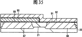
附图35所示为在附图34的步骤之后半导体器件的制造步骤的剖视图;Accompanying drawing 35 is shown in the sectional view of the manufacturing step of semiconductor device after the step of accompanying drawing 34;
附图36所示为在附图35的步骤之后半导体器件的制造步骤的剖视图;Accompanying drawing 36 is shown in the sectional view of the manufacturing step of semiconductor device after the step of accompanying drawing 35;
附图37所示为在附图36的步骤之后半导体器件的制造步骤的剖视图;Accompanying drawing 37 is shown in the sectional view of the manufacturing step of semiconductor device after the step of accompanying drawing 36;
附图38所示为由本发明人调查的半导体器件的制造步骤的剖视图;Figure 38 is a cross-sectional view showing the manufacturing steps of the semiconductor device investigated by the present inventors;
附图39所示为在附图38的步骤之后半导体器件的制造步骤的剖视图;Accompanying drawing 39 is shown in the sectional view of the manufacturing step of semiconductor device after the step of Fig. 38;
附图40所示为在附图39的步骤之后半导体器件的制造步骤的剖视图;Accompanying drawing 40 is shown in the sectional view of the manufacturing step of semiconductor device after the step of Fig. 39;
附图41所示为在附图40的步骤之后半导体器件的制造步骤的剖视图;Accompanying drawing 41 is shown in the sectional view of the manufacturing step of semiconductor device after the step of Fig. 40;
附图42所示为在附图41的步骤之后半导体器件的制造步骤的剖视图;Accompanying drawing 42 is shown in the cross-sectional view of the manufacturing step of semiconductor device after the step of accompanying drawing 41;
附图43所示为在附图42的步骤之后半导体器件的制造步骤的剖视图;Accompanying drawing 43 is shown in the sectional view of the manufacturing step of semiconductor device after the step of accompanying drawing 42;
附图44所示为由本发明人调查的半导体器件的制造步骤的剖视图;Figure 44 is a sectional view showing the manufacturing steps of the semiconductor device investigated by the present inventors;
附图45所示为在附图44的步骤之后半导体器件的制造步骤的剖视图;Accompanying drawing 45 is shown in the sectional view of the manufacturing step of semiconductor device after the step of accompanying drawing 44;
附图46所示为在附图45的步骤之后半导体器件的制造步骤的剖视图;Accompanying drawing 46 is shown in the sectional view of the manufacturing step of semiconductor device after the step of accompanying drawing 45;
附图47所示为在附图46的步骤之后半导体器件的制造步骤的剖视图;Accompanying drawing 47 is shown in the cross-sectional view of the manufacturing step of semiconductor device after the step of Fig. 46;
附图48所示为在附图47的步骤之后半导体器件的制造步骤的剖视图;Accompanying drawing 48 is shown in the sectional view of the manufacturing step of semiconductor device after the step of Fig. 47;
附图49所示为在附图48的步骤之后半导体器件的制造步骤的剖视图。FIG. 49 is a sectional view showing a manufacturing step of the semiconductor device after the step of FIG. 48 .
具体实施方式Detailed ways
在下文描述的实施例中,如为了方便的目的有必要分为多个部分或多个实施例进行描述。这些多个部分或实施例彼此之间并非独立的,而是处于这样的一种关系:一个是另一个的一部分或全部的改进实例、细节或补充描述,除非另有说明。In the embodiments described below, if it is necessary for the purpose of convenience, it is divided into a plurality of parts or described in a plurality of embodiments. These plural parts or embodiments are not independent of each other, but are in such a relationship that one is a modified example, detail or supplementary description of a part or the whole of the other, unless otherwise specified.
在下文的实施例中,在提到元件的数量(包括数量、数值、多少和范围),元件的数量并不限于特定的数目,而是可以多于或少于特定的数量,除非另外专门指出或者在本质上该数量显然限于特定的数目的情况之外。In the following embodiments, when referring to the number of elements (including quantity, value, number and range), the number of elements is not limited to a specific number, but may be more or less than a specific number, unless otherwise specifically indicated Or outside the case where the number is clearly limited to a specific number in nature.
此外,在下文描述的实施例中,不用说这些组成元件(包括元件步骤)并非总是关键的,除非另外专门指出或者本质上它们显然是关键的情况之外。Furthermore, in the embodiments described below, it is needless to say that these constituent elements (including element steps) are not always critical unless otherwise specifically indicated or in a case where they are obviously critical in nature.
类似地,在下文描述的实施例中,在提到组成元件的形状或位置关系时,与其基本类似或相似的也被包含在其中,除非另外专门指出或在原理上它们完全不同的情况之外。这也适用于上文描述的值和范围。Similarly, in the embodiments described below, when referring to the shape or positional relationship of constituent elements, those substantially similar or similar thereto are also included unless otherwise specifically indicated or they are completely different in principle . This also applies to the values and ranges described above.
在示出的实施例的所有附图中,通过相似的参考编号标示相同的部件,并省去重复的描述。In all the drawings of the illustrated embodiments, the same components are designated by like reference numerals, and repeated descriptions are omitted.
下文基于附图更具体地描述本发明的实施例。Embodiments of the present invention are described in more detail below based on the drawings.
(实施例1)(Example 1)
在实施例1中,本发明适用于配备有以相对较低的电压驱动的低击穿电压MISFET(金属绝缘体半导体)和以相对较高的电压驱动的高击穿电压MISFET以实现高压操作并具有可编程的非易失性存储器的半导体器件;及其制造方法。在MISFET中,术语“击穿电压”意味着在构成MISFET的源极区和半导体衬底(阱)之间或者在漏极区和半导体衬底(阱)之间的边界上产生的pn结击穿电压、或者栅极绝缘膜的耐压。在实施例1中,具有相对较高的击穿电压的高击穿电压MISFET和具有相对较低的击穿电压的低击穿电压MISFET形成在一个半导体衬底之上。In Embodiment 1, the present invention is applied to a device equipped with a low breakdown voltage MISFET (Metal Insulator Semiconductor) driven at a relatively low voltage and a high breakdown voltage MISFET driven at a relatively high voltage to achieve high voltage operation and has Semiconductor device of programmable non-volatile memory; and manufacturing method thereof. In MISFET, the term "breakdown voltage" means a pn junction strike that occurs at the boundary between the source region and the semiconductor substrate (well) or between the drain region and the semiconductor substrate (well) constituting the MISFET breakdown voltage, or the withstand voltage of the gate insulating film. In Embodiment 1, a high breakdown voltage MISFET having a relatively high breakdown voltage and a low breakdown voltage MISFET having a relatively low breakdown voltage are formed over one semiconductor substrate.
下文参考附图1至3描述本实施例中的半导体构成。The semiconductor configuration in this embodiment is described below with reference to FIGS. 1 to 3 .
附图1所示为形成在芯片(半导体衬底)1上的元件的布局结构的顶视图。在附图1中,芯片1具有CPU(中央处理单元)2、ROM(只读存储器)3、RAM(随机存取存储器)4、EEPROM(电可擦除的可编程的只读存储器)5、模拟电路6和静电保护电路7a至7g。FIG. 1 is a top view showing a layout structure of elements formed on a chip (semiconductor substrate) 1 . In accompanying drawing 1, chip 1 has CPU (central processing unit) 2, ROM (read-only memory) 3, RAM (random access memory) 4, EEPROM (electrically erasable programmable read-only memory) 5, An
CPU(电路)2也被称为中央处理单元,它是计算机的心脏。这个CPU 2从存储器器件中读取指令,并基于这些指令,执行各种操作或控制。它被要求具有高速处理特性。在形成于芯片1上的元件中,构成CPU 2的MISFET需要相对较高的电流驱动力。换句话说,它由低击穿电压MISFET构成。CPU (circuit) 2 is also called a central processing unit, which is the heart of a computer. This
ROM(电路)3是一种以永久的形式存储数据的存储器,不能改变这种存储器中所存储的数据。它称为只读存储器。ROM 3具有两种类型的构成,即串联连接MISFET的NAND型号和并联连接MISFET的NOR型号。在要求较高的集成度时和在要求高速操作时通常分别使用NAND型和NOR型。ROM 3也被要求高速操作以使构成ROM 3的MISFET必须具有相对较高的电流驱动力。换句话说,ROM 3由低电压MISFET构成。ROM (circuit) 3 is a memory that stores data in a permanent form, and data stored in such a memory cannot be changed. It's called read-only memory. ROM 3 has two types of configurations, a NAND type in which MISFETs are connected in series and a NOR type in which MISFETs are connected in parallel. The NAND type and the NOR type are generally used when a higher degree of integration is required and when high-speed operation is required, respectively. ROM 3 is also required to operate at high speed so that the MISFETs constituting ROM 3 must have a relatively high current drive force. In other words, ROM 3 consists of low voltage MISFETs.
RAM(电路)4是一种能够随机地读取所存储的数据(这意味着随时读取所存储的数据)或者重新写所存储的数据的存储器。它也被称为随机存取存储器。RAM作为IC存储器具有两种类型,即使用动态电路的DRAM(动态RAM)和使用静态电路的SRAM(静态RAM)。DRAM是需要存储器保持操作的随机存取存储器,而SRAM是不需要存储器保持操作的随机存取存储器。由于RAM 4需要高速操作,因此构成RAM 4的MISFET被要求具有相对较高的电流驱动力。换句话说,它由低击穿电压的MISFET构成。The RAM (circuit) 4 is a memory capable of randomly reading stored data (which means reading stored data at any time) or rewriting stored data. It is also known as Random Access Memory. RAM has two types as IC memory, DRAM (Dynamic RAM) using a dynamic circuit and SRAM (Static RAM) using a static circuit. DRAM is a random access memory that requires memory retention operations while SRAM is a random access memory that does not require memory retention operations. Since RAM 4 requires high-speed operation, the MISFETs constituting RAM 4 are required to have a relatively high current driving force. In other words, it consists of MISFETs with low breakdown voltage.
EEPROM 5是一种能够电重写写操作和擦除操作两种操作的非易失性存储器。它也被称为电可擦除可编程只读存储器。这个EEPROM 5的存储器单元由用于存储器的晶体管比如MONOS(金属氧化物氮化物氧化物半导体)晶体管或MNOS(金属氮化物氧化物半导体)晶体管构成。EEPROM 5例如利用Fowler-Nordheim隧道现象进行其写操作和擦除操作。它也利用热电子或热空穴进行其写操作或擦除操作。
在EEPROM 5执行写操作时,在用于存储器的MONOS晶体管中产生高电位差(大约12V)以使具有相对较高的击穿电压的晶体管必须作为用于存储器的MONOS晶体管。When the
模拟电路6是处理显示连续的与时间相关的变化的电压或电流的信号(即模拟信号)的电路。它例如由放大电路、变换电路、调制电路、振荡电路和电源电路构成。在形成在芯片1上的元件中,具有相对较高的击穿电压的高击穿电压MISFET被用于模拟电路6。The
静电保护电路7a至7g是安装在外部端子上的电路以便防止内部电路的破坏,否则可能由来自元件或绝缘膜的带电电荷的发射产生的热量或电压造成破坏。带电电荷的实例包括在人体或目标中累积的静电电荷。静电保护电路7a和7c安装在输入/输出端子上,而静电保护电路7b安装在监测端子上。静电保护电路7d安装在Vss端子上,而静电保护电路7e安装在CLK(时钟)端子上。静电保护电路7f安装在RST(复位)端子上,而静电保护电路7g安装在Vcc端子上。由于高压被施加给这些静电保护电路7a和7c至7g,因此,在形成于芯片1上的元件中,具有相对较高的击穿电压的高击穿电压MISFET用于它们。The static electricity protection circuits 7a to 7g are circuits mounted on external terminals in order to prevent destruction of internal circuits that might otherwise be caused by heat or voltage generated by emission of charged charges from elements or insulating films. Examples of charged charges include electrostatic charges accumulated in a human body or object. The static electricity protection circuits 7a and 7c are mounted on the input/output terminals, and the static electricity protection circuit 7b is mounted on the monitor terminal. The static electricity protection circuit 7d is mounted on the Vss terminal, and the static electricity protection circuit 7e is mounted on the CLK (clock) terminal. The static electricity protection circuit 7f is mounted on the RST (reset) terminal, and the static electricity protection circuit 7g is mounted on the Vcc terminal. Since a high voltage is applied to these electrostatic protection circuits 7a and 7c to 7g, among elements formed on the chip 1, high breakdown voltage MISFETs having a relatively high breakdown voltage are used for them.
在附图2中示出附图1的EEPROM 5的内部构成的一个实例。在附图2中,EEPROM 5具有存储器阵列10,并且具有用于存储器阵列10的直接外围电路单元11和间接外围电路单元12作为用于驱动存储器阵列的驱动电路。An example of the internal constitution of the
存储器阵列10是EEPROM 5的存储器部分,它具有以二维矩阵形式设置的大量的存储器单元。存储器单元是存储1比特作为一个单元信息的电路,它由MONOS晶体管(它是存储器部分)构成。The
驱动电路是一种用于驱动存储器阵列10的电路,它具有用于将来自电源的电压电平提高几倍的升压器电路、用于升压的时钟发生器电路、电压箝位电路、用于选择行或列的列解码器或行解码器、列锁存电路和WELL控制电路作为直接外围电路单元11。构成直接外围电路单元11的MISFET每个由高击穿电压MISFET形成,在形成于芯片1上的元件中它要求相对较高的击穿电压。The driving circuit is a circuit for driving the
间接外围电路单元12形成为存储器阵列的可编程的控制器电路,它具有构造电路,用于普通使用的可编程时钟发生器电路、用于高速使用的可编程时钟发生器电路和可编程的时序控制器电路。间接外围电路单元12由可以以较低的电压驱动的低压MISFET构成,并且在形成于芯片1上的元件中它以较高的速度操作。The indirect
附图3所示为形成在芯片1上的MONOS晶体管Q1、低击穿电压MISFET Q2、高击穿电压MISFET Q3和电容器元件C的剖视图。附图3中的存储器单元形成区对应于在其中已经形成了MONOS晶体管Q1的EEPROM(可编程非易失性存储器)5中的多个存储器单元形成区中的每一个。低击穿电压MISFET形成区是其中已经形成了要求高电流驱动力以实现高速操作的低击穿电压MISFET Q2的区域。CPU 2和RAM 4的形成区被作为这样的区域的实例:其中已经形成了低击穿电压MISFET Q2。低击穿电压MISFET在大约1.5V的电源电压下工作。高击穿电压MISFET形成区是其中已经形成了高击穿电压MISFET Q3的区域,并且这种区域的实例包括模拟电路6的形成区和其中已经形成了在EEPROM 5中的驱动电路(比如解码器)的区域。这种高击穿电压MISFET Q3在大约5V的电源电压下工作。在电容器元件形成区中,已经形成了构成电路的电容器元件。电容器元件例如由PIP(多晶硅绝缘体多晶硅)形成。3 is a cross-sectional view of MONOS transistor Q1, low breakdown voltage MISFET Q2, high breakdown voltage MISFET Q3 and capacitor element C formed on chip 1. The memory cell formation region in FIG. 3 corresponds to each of a plurality of memory cell formation regions in the EEPROM (Programmable Nonvolatile Memory) 5 in which the MONOS transistor Q1 has been formed. The low-breakdown-voltage MISFET formation region is a region in which the low-breakdown-voltage MISFET Q2 that requires high current driving force for high-speed operation has been formed. The formation area of the
如附图3所示,用于隔离元件的元件隔离区21形成在半导体衬底20中,通过元件隔离区21隔离的活性区分别是存储器单元形成区、低击穿电压MISFET形成区和高击穿电压MISFET形成区。在存储器单元形成区、低击穿电压MISFET形成区和高击穿电压MISFET形成区的半导体衬底20中,形成了将会是阱隔离层的n型半导体区22。这些阱已经形成在这种n型半导体区22中。例如,在存储器单元形成区中,p阱23形成在n型半导体区22中。在低击穿电压MISFET形成区中,p阱24形成在n型半导体区22中。在高击穿电压MISFET形成区中,p阱25形成在n型半导体区22中。在存储器单元形成区中形成的p阱23和在高击穿电压MISFET形成区中形成的p阱25都以相同的步骤形成并具有相等的杂质浓度,因为存储器单元和高击穿电压MISFET在例如施加到其中的电压等条件方面类似。另一方面,低击穿电压MISFET和高击穿电压MISFET在例如施加到其中的电压等条件方面不同,这样在低击穿电压MISFET形成区中形成的p阱24的杂质浓度因此与p阱23或p阱25的杂质浓度不同。As shown in FIG. 3, an
在本实施例1中,示出了n沟道MISFET,该n沟道MISFET被描述为形成在低击穿电压MISFET形成区和高击穿电压MISFET形成区的每个区中形成的MISFET,但是p沟道MISFET也被形成在这些区中。In the present embodiment 1, an n-channel MISFET is shown, which is described as a MISFET formed in each of the low breakdown voltage MISFET formation region and the high breakdown voltage MISFET formation region, but P-channel MISFETs are also formed in these regions.
接着描述在附图3中示出的MONOS晶体管Q1的构成。Next, the constitution of the MONOS transistor Q1 shown in FIG. 3 will be described.
在存储器单元形成区中形成的MONOS晶体管Q1具有如下的结构。具体地描述,栅极绝缘膜26已经形成在半导体衬底20上形成的p阱23中,并且电荷存储膜27已经形成在栅极绝缘膜26上。绝缘膜(电位阻挡膜)28已经形成在电荷存储膜27上,由导电膜形成的栅电极44已经形成在绝缘膜28上。栅电极44例如由多晶硅膜29和硅化钴膜56层叠成的膜形成以便降低电阻,并且形成在栅电极44两侧的侧壁上,已经被形成了例如由绝缘膜形成的侧壁51以构成LDD(轻掺杂的漏极)结构。The MONOS transistor Q1 formed in the memory cell formation region has the following structure. Described specifically,
在侧壁51之下的半导体衬底20中,轻掺杂的n型杂质扩散区48和重掺杂的n型杂质扩散区53都已经形成为半导体区。直接在栅极绝缘膜26之下的p阱23中,已经形成了由n型半导体区形成的沟道形成区。In the
在具有这种结构的MONOS晶体管Q1中,栅极绝缘膜26已经例如由氧化硅膜形成,并且它也具有作为隧道绝缘膜的功能。例如,通过经栅极绝缘膜26将电子从半导体衬底20注入到电荷存储膜27中或者将电子从电荷存储膜27喷射进半导体衬底20中,这个MONOS晶体管Q1存储或擦除数据,因此栅极绝缘膜26用作隧道绝缘膜。In the MONOS transistor Q1 having such a structure, the
电荷存储膜27是被设置成存储对数据存储有贡献的电荷的膜,并且例如由氮化硅膜形成。The
多晶硅膜通常被用作电荷存储膜27。然而,在多晶硅膜被用作电荷存储膜27时,在包含电荷存储膜27的氧化膜的部分中的缺陷的存在导致了异常泄漏,在电荷存储膜27中存储的所有电荷可以从其中逃逸,因为电荷存储膜27是导体。A polysilicon film is generally used as the
如上文所述,作为绝缘体的氮化硅已经被用作电荷存储膜27。在这种情况下,对数据存储器有贡献的电荷以在氮化硅膜中存在的离散的俘获电平(俘获电平)被存储。即使缺陷出现在包含了电荷存储膜27的氧化物膜的一部分中,电荷仍然以电荷存储膜27的离散的俘获电平存储以使不会使电荷从电荷存储膜27中逃逸。因此提高了数据保持的可靠性。As described above, silicon nitride as an insulator has been used as the
因为上述的原因,不仅由氮化硅膜而且由包含了离散的俘获电平的膜形成的电荷存储膜27的使用对于提高数据保持的可靠性是有用的。For the reasons described above, use of the
侧壁51已经被形成为将LDD结构赋予给源极和漏极区,这里的源极和漏极区都是MONOS晶体管Q1的半导体区。MONOS晶体管Q1的源极和漏极区已经由轻掺杂的n型杂质扩散区48和重掺杂的n型杂质扩散区53形成。由于轻掺杂的n型杂质扩散区48已经被形成为在侧壁51之下的源极和漏极区,因此可以抑制在栅电极44的端部部分之下的电场浓度。
下文接着描述附图3中所示的低击穿电压MISFET Q2的结构。在低击穿电压MISFET Q2中,栅极绝缘膜36已经形成在半导体衬底20中形成的p阱24上,并且栅电极39已经形成在这个栅极绝缘膜36上。栅极绝缘膜36例如由氧化硅膜形成,而栅电极39由多晶硅膜37和硅化钴膜56层叠成的膜形成以便降低其电阻。Next, the structure of the low breakdown voltage MISFET Q2 shown in FIG. 3 will be described. In the low breakdown voltage MISFET Q2, the
在栅电极39的两侧的侧壁上,已经形成了侧壁52。在侧壁52之下的半导体衬底20中,轻掺杂的n型杂质扩散区49和重掺杂的n型杂质扩散区54已经形成为半导体区。直接在栅极绝缘膜36之下的p阱24中,已经形成了由p型半导体区形成的沟道形成区。On the sidewalls on both sides of the
下文接着描述附图3中所示的高击穿电压MISFET Q3的结构。在高击穿电压MISFET Q3中,栅极绝缘膜34已经形成在半导体衬底20中形成的p阱25上,并且栅电极40已经形成在这个栅极绝缘膜34上。栅极绝缘膜34例如由氧化硅膜形成,而栅电极40由多晶硅膜37和硅化钴膜56层叠成的膜形成以便降低其电阻。Next, the structure of the high breakdown voltage MISFET Q3 shown in FIG. 3 will be described below. In the high breakdown voltage MISFET Q3, the
在栅电极40的两侧的侧壁上,已经形成了侧壁51。在侧壁51之下的半导体衬底20中,轻掺杂的n型杂质扩散区50和重掺杂的n型杂质扩散区55已经形成为半导体区。直接在栅极绝缘膜34之下的p阱25中,已经形成了由p型半导体区形成的沟道形成区。On sidewalls on both sides of the
接着描述低击穿电压MISFET Q2和高击穿电压MISFET Q3之间的区别。首先,高击穿电压MISFET Q3的侧壁51具有比低击穿电压MISFET Q2的侧壁52更大的宽度。由于在操作时相对较大的电位差(大约5V)施加给高击穿电压MISFET Q3,因此使侧壁51的宽度相对较大以改善在源极漏极区和半导体衬底(p阱25)之间的pn结击穿电压。另一方面,在操作时仅仅相对较低的电位差(大约1.5V)被施加给低击穿电压MISFET Q2以使侧壁52的宽度相对较小以便改善高速操作。Next, the difference between the low breakdown voltage MISFET Q2 and the high breakdown voltage MISFET Q3 will be described. First, the
第二,高击穿电压MISFET Q3的栅电极40比低击穿电压MISFET Q2的栅电极39具有更大的栅极长度。在低击穿电压MISFETQ2中,栅电极39的栅极长度必须降低以减小在源极区和漏极区之间的电阻,由此改善电流驱动功率。另一方面,在高击穿电压MISFET Q3中,因为由于施加到其中的相对较高的电位的缘故,栅极长度的减小在源极和漏极区之间不可避免地产生穿通现象,所以使栅极长度更长。Second, the
第三,高击穿电压MISFET Q3的栅极绝缘膜34比低击穿电压MISFET Q2的栅极绝缘膜36更厚,因为施加到前者的电压高于施加到后者的电压。高击穿电压MISFET Q3的栅极绝缘膜34因此改善了绝缘电阻。Third, the
接着描述在附图3中所示的电容器元件C的构成。电容器元件C具有例如由多晶硅膜形成的下部电极33,电容器绝缘膜已经形成在下部电极33上。电容器绝缘膜由层叠的绝缘膜形成,例如氧化硅膜30、氮化硅膜31和氧化硅膜40层叠成的膜。电容器绝缘膜具有由例如多晶硅膜形成的上部电极42。在下部电极33和上部电极42的表面上,已经形成了硅化钴膜56。通过控制电容器绝缘膜的厚度和下部电极42和上部电极33的面积,电容器元件C具有所需的电容。Next, the constitution of the capacitor element C shown in FIG. 3 will be described. The capacitor element C has a
在MONOS晶体管Q1、低击穿电压MISFET Q2、高击穿电压MISFET Q3和电容器元件C上,已经形成了由氮化硅膜57和氧化硅膜58形成的层间绝缘膜。在层间绝缘膜中,已经形成了接触孔59。已经形成了插塞60以便将其填埋在接触孔59中。插塞60例如由作为阻挡膜的钛/氮化钛膜和钨膜形成。在具有其中形成的插塞60的层间绝缘膜上,已经形成了由铝膜或铝合金膜形成的互连61。On the MONOS transistor Q1, the low breakdown voltage MISFET Q2, the high breakdown voltage MISFET Q3, and the capacitor element C, an interlayer insulating film formed of a
实施例1的半导体器件具有如上文所述的结构。接着描述实施例1的特征结构。在附图3中,本发明的一个特征在于防止在MONOS晶体管Q1、低击穿电压MISFET Q2和高击穿电压MISFET Q3的每个中形成鸟嘴。The semiconductor device of Embodiment 1 has the structure as described above. Next, the characteristic structure of Embodiment 1 will be described. In FIG. 3, one feature of the present invention is to prevent bird's beak formation in each of the MONOS transistor Q1, the low breakdown voltage MISFET Q2, and the high breakdown voltage MISFET Q3.
根据常规的制造方法,MONOS晶体管的栅电极和用于外围电路的MISFET(低击穿电压MISFET和高击穿电压MISFET)中的每个的栅电极通过如下过程形成:在其上处理、淀积栅极绝缘膜和导体膜获得一个栅电极,然后通过处理获得另一个栅电极。在形成了另一个栅电极时因此氧化首先形成的栅电极的表面。具体地说,鸟嘴出现在首先形成的栅电极和半导体衬底之间,并增加了在其端部部分上的栅极绝缘膜的厚度。例如,在首先形成的栅电极是MONOS晶体管时,MONOS晶体管的栅极绝缘膜在电子注入到电荷存储膜中或者从其中喷射出的过程中用作隧道绝缘膜。由于形成了鸟嘴引起的栅极绝缘膜所增加的厚度因此干扰了隧道现象的发生,进一步干扰了电子到电荷存储膜的注入或者电子自其中喷射出来。这延迟了数据的写入或擦除,因此使MONOS晶体管的特性劣化。另一方面,在首先形成的栅电极是用于外围电路的MISFET时,鸟嘴的产生也劣化它的特性。According to a conventional manufacturing method, a gate electrode of a MONOS transistor and a gate electrode of each of MISFETs (low breakdown voltage MISFET and high breakdown voltage MISFET) used in peripheral circuits are formed by processing, depositing The gate insulating film and the conductor film obtain one gate electrode, and then the other gate electrode is obtained by processing. When another gate electrode is formed, the surface of the first formed gate electrode is thus oxidized. Specifically, a bird's beak appears between the first formed gate electrode and the semiconductor substrate, and increases the thickness of the gate insulating film on its end portion. For example, when the gate electrode formed first is a MONOS transistor, the gate insulating film of the MONOS transistor functions as a tunnel insulating film during electron injection into or ejection from the charge storage film. The increased thickness of the gate insulating film due to the formation of the bird's beak thus interferes with the occurrence of the tunneling phenomenon, further disturbing the injection of electrons into or ejection of electrons from the charge storage film. This delays writing or erasing of data, thus deteriorating the characteristics of the MONOS transistor. On the other hand, when the gate electrode formed first is a MISFET for a peripheral circuit, the generation of the bird's beak also deteriorates its characteristics.
在实施例1中,通过利用如下的制造方法防止产生鸟嘴,即,-在MONOS晶体管的栅电极和用于外围电路的MISFET的栅电极的形成处理之前,-形成用于MONOS晶体管的栅电极的形成的导体膜和用于外围电路的MISFET的栅电极的形成的导体膜,然后将它们处理成MONOS晶体管的栅电极和用于外围电路的MISFET的栅电极。因此,在两种晶体管中都可能防止产生鸟嘴,由此改善了半导体器件的可靠性。在利用这种制造方法时,虚图形45形成在存储器单元形成区和用于外围电路的MISFET形成区(在附图3中的低击穿电压MISFET形成区)之间的边界区中。结果,实施例1的制造方法在边界区中留下了虚图形45作为其印痕。虚图形可以被变形或清除,这取决于如何对抗蚀剂图形进行构图。附图3所示为使用实施例1的半导体器件的制造方法的一个实例,在这个实例中已经形成了虚图形45。In Embodiment 1, the bird's beak is prevented from being generated by utilizing a manufacturing method in which - before the formation process of the gate electrode of the MONOS transistor and the gate electrode of the MISFET for the peripheral circuit, - the gate electrode for the MONOS transistor is formed The formed conductor film and the gate electrode of the MISFET used for the peripheral circuit are then processed into the gate electrode of the MONOS transistor and the gate electrode of the MISFET used for the peripheral circuit. Therefore, it is possible to prevent the generation of bird's beaks in both transistors, thereby improving the reliability of the semiconductor device. When using this manufacturing method, the
根据实施例1的半导体器件具有如上文所描述的结构。接着参考附图描述在这个半导体器件中描述的存储器单元(非易失性存储器单元)的操作。The semiconductor device according to Embodiment 1 has the structure as described above. Next, the operation of the memory cell (nonvolatile memory cell) described in this semiconductor device will be described with reference to the drawings.
附图4所示为在附图1中所示的EEPROM 5的存储器阵列结构和操作条件(1个单元/1个晶体管)的一个实例的示意图。在附图4中所示的每个存储器单元是由电荷累积晶体管单独构成的存储器单元的一个实例。Accompanying drawing 4 is shown in the schematic diagram of an example of the memory array structure and operation condition (1 cell/1 transistor) of
存储器单元由在附图3中所示的MONOS晶体管形成,并具有如附图4所示的单元晶体管CT1至CT8。单元晶体管CT1至CT8的栅电极连接到字线WL1至WL2并且它们的源极区连接到源极线SL1至SL4。它们的漏极区连接到数据线DL1至DL4。单元晶体管CT1、CT2、CT5和CT6的背栅连接到阱WE1,而单元晶体管CT3、CT4、CT7和CT8的背栅连接到阱WE2。The memory cell is formed of MONOS transistors as shown in FIG. 3 and has cell transistors CT1 to CT8 as shown in FIG. 4 . Gate electrodes of the cell transistors CT1 to CT8 are connected to word lines WL1 to WL2 and their source regions are connected to source lines SL1 to SL4 . Their drain regions are connected to the data lines DL1 to DL4. The back gates of the cell transistors CT1, CT2, CT5, and CT6 are connected to the well WE1, and the back gates of the cell transistors CT3, CT4, CT7, and CT8 are connected to the well WE2.
为了简化描述,存储器单元在附图4中以两行和四列设置,但它们不限于此。实际中,更多的存储器单元以矩阵形式设置以构成存储器阵列。在附图4中,共享相同阱和相同字线的存储器单元结构是例如由单元晶体管CT1和CT2构成的两列结构。在8-位(1字节)结构中,8列单元晶体管共享相同的阱。在这种情况下,一次一个字节地执行存储器单元的擦除和写入操作。For simplicity of description, memory cells are arranged in two rows and four columns in FIG. 4, but they are not limited thereto. In practice, more memory cells are arranged in a matrix to form a memory array. In FIG. 4, the memory cell structure sharing the same well and the same word line is, for example, a two-column structure composed of cell transistors CT1 and CT2. In an 8-bit (1 byte) structure, 8 columns of cell transistors share the same well. In this case, erase and write operations of memory cells are performed one byte at a time.
下文基于附图4描述1个单元/1个晶体管型存储器单元的擦除、写入和读取操作。The erase, write, and read operations of 1 cell/1 transistor type memory cell are described below based on FIG. 4 .
首先,假设如下情况描述擦除操作:选择了要被擦除其数据的存储器单元(所选择的存储器单元)并擦除了在其单元晶体管CT1和CT2中存储的数据。所选择的阱WE1、字线WL1、源极线SL1,SL2和数据线DL1,DL2的电位被分别调节到1.5V、-8.5V、1.5V和浮动电位。在单元晶体管CT1和CT2的电荷存储膜中存储的电荷然后被提取到半导体衬底侧并擦除数据。关于没有擦除其数据的其它存储器单元(未被选择的存储器单元)的单元晶体管CT3至CT8,未被选择的阱WE2、字线WL2、源极线SL3,SL4和数据线DL3,DL4的电位被分别设定到-8.5V、1.5V、1.5V和浮动电位。因此防止了在单元晶体管CT3至CT8的电荷存储膜中存储的电荷逃逸,由此不擦除数据。First, an erase operation is described assuming a case where a memory cell whose data is to be erased (selected memory cell) is selected and data stored in its cell transistors CT1 and CT2 is erased. The potentials of the selected well WE1, word line WL1, source lines SL1, SL2 and data lines DL1, DL2 are adjusted to 1.5V, -8.5V, 1.5V and floating potential, respectively. Charges stored in the charge storage films of the cell transistors CT1 and CT2 are then extracted to the semiconductor substrate side and data is erased. Regarding the cell transistors CT3 to CT8 of other memory cells (unselected memory cells) whose data is not erased, the potentials of the unselected well WE2, word line WL2, source lines SL3, SL4, and data lines DL3, DL4 are set to -8.5V, 1.5V, 1.5V and floating potential respectively. Thus, the charges stored in the charge storage films of the cell transistors CT3 to CT8 are prevented from escaping, thereby not erasing data.
接着,假设如下的情况描述写入操作:选择要被写入数据的存储器单元(所选择的存储器单元)并将数据写入在其单元晶体管CT1中。所选择的阱WE1、字线WL1、源极线SL1和数据线DL1的电位被分别设定到-10.5V、1.5V、-10.5V和浮动电位。电荷被注入到单元晶体管CT1的电荷存储膜中并将数据写入其中。关于没有被写入数据的单元晶体管CT2至CT8(未被选择的存储器单元),未被选择的阱WE2、字线WL2、源极线SL2至4和数据线DL2至4的电位被分别设置到-10.5V、-10.5V、1.5V和浮动电位。因此防止了电荷注入到单元晶体管CT2至8的电荷存储膜中。Next, the writing operation will be described assuming a case where a memory cell to which data is to be written (selected memory cell) is selected and data is written in its cell transistor CT1. The potentials of the selected well WE1, word line WL1, source line SL1, and data line DL1 are set to -10.5V, 1.5V, -10.5V and floating potential, respectively. Charges are injected into the charge storage film of the cell transistor CT1 and data is written therein. Regarding the cell transistors CT2 to CT8 (unselected memory cells) in which data is not written, the potentials of the unselected well WE2, word line WL2, source lines SL2 to 4, and data lines DL2 to 4 are respectively set to -10.5V, -10.5V, 1.5V and floating potentials. Charge injection into the charge storage films of the cell transistors CT2 to 8 is thus prevented.
接着,例如假设如下的情况描述读取操作:在单元晶体管CT1中的数据“1”的写入已增加了晶体管的阈值电压,而在单元晶体管CT2中的数据“0”已降低了阈值电压。在从单元晶体管CT1和2中读出数据时,所选择的阱WE1、字线WL1、源极线SL1和SL2和数据线DL1和DL2的电位分别被设定为-2V、0V、0V和1V。在这种方式中,数据从单元晶体管CT1和CT2中读出。在这种情况下,由于单元晶体管CT1的阈值电压较高而单元晶体管CT2的阈值电压较低,因此数据线DL2的电位降低而不改变数据线DL1的电位。关于从其中没有读出数据的其它单元晶体管CT3至CT8,未被选择的阱WE2、字线WL2、源极线SL3,SL4和数据线DL3和DL4的电位分别被设定为-2V、-2V、0V和0V,由此防止了单元晶体管CT3到CT8接通。通过在读取操作中降低未被选择的存储器单元的背栅电位,存储器单元不需要所选择的晶体管。Next, the read operation is described assuming, for example, that writing of data "1" in the cell transistor CT1 has increased the threshold voltage of the transistor and data "0" in the cell transistor CT2 has lowered the threshold voltage. When reading data from the cell transistors CT1 and 2, the potentials of the selected well WE1, word line WL1, source lines SL1 and SL2, and data lines DL1 and DL2 are set to -2V, 0V, 0V, and 1V, respectively. . In this manner, data is read from the cell transistors CT1 and CT2. In this case, since the threshold voltage of the cell transistor CT1 is high and the threshold voltage of the cell transistor CT2 is low, the potential of the data line DL2 is lowered without changing the potential of the data line DL1. Regarding the other cell transistors CT3 to CT8 from which data is not read out, the potentials of the unselected well WE2, word line WL2, source lines SL3, SL4, and data lines DL3 and DL4 are set to -2V, -2V, respectively. , 0V, and 0V, thereby preventing the cell transistors CT3 to CT8 from being turned on. By lowering the back gate potential of unselected memory cells in a read operation, the memory cells do not require selected transistors.
下文参考附图描述根据实施例1的半导体器件的制造方法。在实施例1中,存储器单元形成区对应于第一区,而低击穿电压MISFET形成区和高击穿电压MISFET形成区对应于第二区。换句话说,MONOS晶体管对应于第一MISFET,而低击穿电压MISFET和高击穿电压MISFET每个对应于第二MISFET。A method of manufacturing the semiconductor device according to Embodiment 1 is described below with reference to the drawings. In Embodiment 1, the memory cell formation region corresponds to the first region, and the low breakdown voltage MISFET formation region and the high breakdown voltage MISFET formation region correspond to the second region. In other words, the MONOS transistor corresponds to the first MISFET, and the low breakdown voltage MISFET and the high breakdown voltage MISFET each correspond to the second MISFET.
如附图5所示,制备具有p型杂质比如在单晶硅中引入的硼(B)的半导体衬底20。在半导体衬底20的主表面上,形成了元件隔离区21。元件隔离区21每个例如由氧化硅膜形成,并且可以通过STI(浅沟槽隔离)或LOCOS(硅的局部氧化)形成。附图5所示为通过在半导体衬底20中形成的沟槽中填埋氧化硅根据STI形成的元件隔离区21。As shown in FIG. 5, a
通过使用光刻和离子注入在半导体衬底20中形成n型半导体区22(它是阱隔离层)。例如通过将n型杂质比如磷(P)或砷(As)引入到半导体衬底20中形成n型半导体区22。An n-type semiconductor region 22 (which is a well isolation layer) is formed in the
通过光刻和离子注入,在存储器单元形成区中形成p阱23,而在高击穿电压MISFET形成区中形成p阱25。例如通过将p型杂质比如硼引入到半导体衬底20中形成P阱23和p阱25。这些阱具有相同的极性浓度。然后,通过光刻和离子注入,沟道形成区形成在存储器单元形成区中。例如通过引入n型杂质比如磷(P)或砷(As)可以形成沟道形成区。类似地,在高击穿电压MISFET形成区中形成沟道形成区。例如通过引入p型杂质比如硼(B)可以形成沟道形成区。类似地,通过离子注入,在低击穿电压MISFET形成区中形成p阱24。p阱24例如具有p型杂质,比如引入其中的硼,并具有适合于低击穿电压MISFET的特性的杂质浓度。换句话说,在存储器单元形成区中形成的p阱23和在高击穿电压MISFET形成区中形成的p阱25都具有相同的杂质浓度,而在低击穿电压MISFET形成区中形成的p阱24的极性浓度与p阱23或p阱25的极性浓度不同。然后在p阱24的表面上形成沟道形成区。这个沟道形成区例如通过在其中引入p型杂质比如硼形成。By photolithography and ion implantation, p well 23 is formed in the memory cell formation region, and p well 25 is formed in the high breakdown voltage MISFET formation region. P well 23 and p well 25 are formed, for example, by introducing p-type impurities such as boron into
如附图6所示,然后在半导体衬底20的主表面上形成栅极绝缘膜(第一电位阻挡膜)26。栅极绝缘膜26例如由氧化硅膜形成,并且通过热氧化形成。然后在栅极绝缘膜26上形成电荷存储膜27。电荷存储膜27例如由氮化硅膜形成,并且可以使用CVD形成,在这种CVD中在硅烷气(SiH4)和氨气(NH3)之间实施化学反应。电荷存储膜27并不限于氮化硅膜,它还可以是其中具有俘获电平的膜,例如氮氧化硅(SiON)膜。As shown in FIG. 6 , a gate insulating film (first potential barrier film) 26 is then formed on the main surface of the
然后在电荷存储膜27上形成绝缘膜(第二电位阻挡膜)28。绝缘膜28例如由氧化硅膜形成,并且可使用CVD形成,在这种CVD中在硅烷气(SiH4)和氧气(O2)之间实施化学反应。因此形成了由栅极绝缘膜26、电荷存储膜27和绝缘膜28构成的绝缘膜叠层(ONO膜,第一绝缘膜)。An insulating film (second potential blocking film) 28 is then formed on the
然后在绝缘膜28上形成多晶硅膜(第一导体膜)29。多晶硅膜29例如可以通过CVD形成,在这种CVD中硅烷气的热分解在氮气(N2)中执行。在形成了多晶硅膜29时,添加导电杂质比如磷。可替换地,在多晶硅膜29的形成完成之后,可以通过离子注入将导电杂质注入到多晶硅膜中。A polysilicon film (first conductor film) 29 is then formed on the insulating
在多晶硅膜29上,形成了由氧化硅膜30、氮化硅膜31和盖层绝缘膜32构成的膜叠层。盖层绝缘膜32例如由氧化硅膜形成。例如通过CVD形成膜叠层。盖层绝缘膜32具有保护在后面的步骤中形成的栅电极44的功能。On the
如附图7所示,通过光刻和蚀刻对栅极绝缘膜26、电荷存储膜27、绝缘膜28、多晶硅膜29、氧化硅膜30、氮化硅膜31和盖层绝缘膜32进行构图。执行构图以将膜叠层留在存储器单元形成区和电容器元件形成区中,同时从低击穿电压MISFET形成区和高击穿电压MISFET形成区中清除膜叠层。通过这种构图,在电容器元件形成区中形成了由多晶硅膜29形成的下部电极33。实施构图以覆盖整个存储器单元形成区并且不执行用于在存储器单元形成区中形成MONOS晶体管的栅电极的处理。这是本发明的一个特性之一。在这种步骤中在存储器单元形成区中形成MONOS晶体管的栅电极时,在MONOS晶体管中不理想地出现了鸟嘴,因为这个步骤之后跟着是例如由氧化硅膜形成的栅极绝缘膜在低击穿电压MISFET形成区和高击穿电压MISFET形成区中的形成(步骤)。在实施例1中,为了防止在MONOS晶体管中产生鸟嘴,将膜叠层留在所有的存储器单元形成区上。As shown in FIG. 7, the
如附图8所示,例如通过热氧化作用在半导体衬底20的整个表面上形成栅极绝缘膜(第二绝缘膜)34。这个栅极绝缘膜34例如由氧化硅膜形成。如附图9所示,在半导体衬底20上形成抗蚀剂图形35。抗蚀剂图形35被构图以便覆盖存储器单元区、高击穿电压MISFET形成区和电容器元件形成区,并暴露出低击穿电压MISFET形成区。通过将抗蚀剂图形35作为掩模,通过蚀刻从低击穿电压MISFET形成区中清除栅极绝缘膜34。As shown in FIG. 8, a gate insulating film (second insulating film) 34 is formed on the entire surface of the
如附图10所示,然后在半导体衬底20上形成栅极绝缘膜(第二绝缘膜)36,由此在低击穿电压MISFET形成区中形成栅极绝缘膜36。在形成了栅极绝缘膜36的步骤之后,在高击穿电压MISFET形成区中形成的栅极绝缘膜34的厚度增加了。这样,在低击穿电压MISFET形成区中形成了相对较薄的栅极绝缘膜36,同时在高击穿电压MISFET形成区中形成了相对较厚的栅极绝缘膜34。As shown in FIG. 10, a gate insulating film (second insulating film) 36 is then formed on the
如附图11所示,然后在栅极绝缘膜34和栅极绝缘膜36上形成多晶硅膜(第二导体膜)37,之后在多晶硅膜37上形成盖层绝缘膜38。例如可以通过CVD形成多晶硅膜37。盖层绝缘膜38例如由氧化硅膜形成,并可以通过例如CVD形成。As shown in FIG. 11 , a polysilicon film (second conductor film) 37 is then formed on the
如附图12所示,通过光刻和蚀刻,在低击穿电压MISFET形成区中形成低击穿电压MISFET的栅电极(第二栅电极)39,而在高击穿电压MISFET形成区中形成高击穿电压MISFET的栅电极(第二栅电极)。一旦蚀刻,清除在存储器单元形成区上形成的栅极绝缘膜34、多晶硅膜37和盖层绝缘膜38。在电容器元件形成区中,对栅极绝缘膜34、多晶硅膜37和盖层绝缘膜38构图以形成电容器绝缘膜和其上形成的上部电极42。电容器绝缘膜由氧化硅膜30、氮化硅膜31和氧化硅膜41形成。通过这种构图,在存储器单元形成区和低击穿电压MISFET形成区之间的边界区中保留了虚图形43。As shown in FIG. 12, by photolithography and etching, the gate electrode (second gate electrode) 39 of the low breakdown voltage MISFET is formed in the low breakdown voltage MISFET formation region, and the gate electrode (second gate electrode) 39 is formed in the high breakdown voltage MISFET formation region. Gate electrode (second gate electrode) of the high breakdown voltage MISFET. Once etched, the
如附图13所示,在半导体衬底20上形成抗蚀剂图形43a。抗蚀剂图形43a已经被构图以覆盖低击穿电压MISFET形成区、高击穿电压MISFET形成区、边界区和电容器元件形成区。抗蚀剂图形43a也形成在存储器单元形成区中的栅电极形成区中,它已经被构图以便暴露除了存储器单元形成区之外的区域。As shown in FIG. 13, a resist pattern 43a is formed on the
如附图14所示,通过以抗蚀剂图形43a作为掩模进行蚀刻,在存储器单元形成区中形成MONOS晶体管的栅电极(第一栅电极)44。这时,在存储器单元形成区和低击穿电压MISFET形成区之间的边界区中形成虚图形45。As shown in FIG. 14, the gate electrode (first gate electrode) 44 of the MONOS transistor is formed in the memory cell formation region by etching with the resist pattern 43a as a mask. At this time, a
这样,MONOS晶体管的栅电极44可以形成在存储器单元形成区中。低击穿电压MISFET的栅电极39可以形成在低击穿电压MISFET形成区中,而高击穿电压MISFET的栅电极40可以形成在高击穿电压MISFET形成区中。In this way, the
根据实施例1,如附图11所示,在没有一个栅电极通过处理形成的情况下,在存储器单元形成区中形成了栅极绝缘膜26、电荷存储膜27、绝缘膜28和多晶硅膜29,而栅极绝缘膜36和34和多晶硅膜37都形成在低击穿电压MISFET形成区和高击穿电压MISFET形成区中。如附图12所示,栅电极39形成在低击穿电压MISFET形成区中,栅电极40形成在高击穿电压MISFET形成区中。由于栅极绝缘膜26、电荷存储膜27、绝缘膜28和多晶硅膜29已经形成在存储器单元形成区中,因此在通过处理形成了栅电极39和40之后,不需要形成栅极绝缘膜26。栅电极39和40在其端部部分处不被氧化,由此可以防止鸟嘴的产生。如附图13所示,然后,在存储器单元形成区中事先形成的栅极绝缘膜26、电荷存储膜27、绝缘膜28和多晶硅膜29被处理以在存储器单元形成区中形成MONOS晶体管的栅电极44。According to Embodiment 1, as shown in FIG. 11, the
通常,在低击穿电压MISFET形成区和高击穿电压MISFET形成区中分别形成了栅电极之后,在半导体衬底的整个表面上形成MONOS晶体管的栅极绝缘膜。在形成MONOS晶体管的栅极绝缘膜时,栅电极在其端部部分处被氧化,在低击穿电压MISFET和高击穿电压MISFET的栅极绝缘膜的端部部分上出现了鸟嘴。在低击穿电压MISFET和高击穿电压MISFET的栅极绝缘膜的端部部分上的鸟嘴的出现造成膜厚增加。低击穿电压MISFET和高击穿电压MISFET的栅极绝缘膜的厚度的增加导致了在低击穿电压MISFET和高击穿电压MISFET的源极区和漏极区之间流动的电流的减小。电流的幅值与栅极绝缘膜的厚度成反比。通过增加栅极绝缘膜的厚度,在源极和漏极区之间流动的电流不能被固定,MISFET不可避免地劣化了特性。此外,由于低击穿电压MISFET变得微小,因此栅电极的栅极长度减小并且短沟道特性比如阈值电压的减小变得突出。栅极绝缘膜越薄,短沟道特性改善越明显。在栅极绝缘膜通过鸟嘴变厚时,短沟道特性变得突出,并且低击穿电压的特性劣化。Usually, the gate insulating film of the MONOS transistor is formed on the entire surface of the semiconductor substrate after gate electrodes are respectively formed in the low breakdown voltage MISFET formation region and the high breakdown voltage MISFET formation region. When forming the gate insulating film of the MONOS transistor, the gate electrode is oxidized at its end portion, and a bird's beak appears on the end portion of the gate insulating film of the low breakdown voltage MISFET and the high breakdown voltage MISFET. The appearance of the bird's beak on the end portion of the gate insulating film of the low breakdown voltage MISFET and the high breakdown voltage MISFET causes the film thickness to increase. The increase in the thickness of the gate insulating film of the low breakdown voltage MISFET and the high breakdown voltage MISFET results in a decrease in the current flowing between the source region and the drain region of the low breakdown voltage MISFET and the high breakdown voltage MISFET . The magnitude of the current is inversely proportional to the thickness of the gate insulating film. By increasing the thickness of the gate insulating film, the current flowing between the source and drain regions cannot be fixed, and the characteristics of the MISFET inevitably deteriorate. Furthermore, since the low breakdown voltage MISFET becomes minute, the gate length of the gate electrode is reduced and short channel characteristics such as reduction in threshold voltage become prominent. The thinner the gate insulating film is, the more obvious the short channel characteristic is improved. When the gate insulating film is thickened by the bird's beak, the short channel characteristic becomes prominent, and the characteristic of low breakdown voltage deteriorates.
在实施例1中,在形成了栅电极39和40之后不需要形成栅极绝缘膜26,因此可以防止在低击穿电压MISFET和高击穿电压MISFET中产生鸟嘴,并可以实现低击穿电压MISFET和高击穿电压MISFET的可靠性的改善。In Embodiment 1, there is no need to form the
根据实施例1,在执行用于MONOS晶体管的栅电极44的形成的处理时,在已经形成的低击穿电压MISFET的栅电极39和高击穿电压MISFET的栅电极40上没有淀积栅极绝缘膜26、电荷存储膜27、绝缘膜28和多晶硅膜29中的任何薄膜,因此蚀刻残余不会保留在栅电极39和40的侧壁上。不需要从首先已经形成的栅电极39和40的侧壁中清除蚀刻残余的步骤,因此栅电极39和40不会受到蚀刻损坏。具体地描述,在蚀刻残余保留在栅电极39和40的侧壁上时,执行干蚀刻以清除这种蚀刻残余。通过这种蚀刻清除蚀刻残余,但在清除蚀刻残余时会担心损坏栅电极39和40的端部部分。然而,在本实施例1中,在事先形成的栅电极39和40的侧壁上不会形成蚀刻残余,因此不需要用于清除蚀刻残余的干蚀刻步骤,因此可保护栅电极39和40不会受到损坏。在实施例1中,如附图14所示,虚图形45仍然保留在存储器单元形成区和高击穿电压MISFET形成区之间的边界区中。它形成在除了元件形成区之外的区域中,因此不会造成任何问题。在实施例1中,虽然形成了虚图形45,但是不必清除它,这意味着不需要增加图形图45的清除步骤。不用增加清除步骤,制造步骤仍然保持简单,而且制造成本不会增加。相反,如果执行清除虚图形45的步骤,则脱落的虚图形可能造成如异物等问题。虚图形45较大,因此本质上不会脱落。从防止产生异物的观点看,优选也留下虚图形。According to Embodiment 1, when the process for forming the
根据抗蚀剂图形的构图,这个虚图形45具有各种形状。如附图14所示的虚图形45可以保留或者如附图15所示的虚图形46可以保留。通过调节抗蚀剂图形,不可能将虚图形保留在如附图16中所示的边界区中。在这种情况下,将在边界区中形成的元件隔离区21的部分被蚀刻成凹部47。This
在常规的方法中,在低击穿电压MISFET的栅电极和高击穿电压MISFET的栅电极形成之后,用于形成MONOS晶体管的栅极绝缘膜、电荷存储膜、绝缘膜和多晶硅膜已经淀积在存储器单元形成区、低击穿电压MISFET形成区和高击穿电压MISFET形成区中的每个区域中。在通过处理形成MONOS晶体管的栅电极时,清除了保留在低击穿电压MISFET形成区和高击穿电压MISFET形成区中的多晶硅膜、绝缘膜、电荷存储膜和栅极绝缘膜。在清除由氮化硅膜形成的电荷存储膜时,位于电荷存储膜之下的氧化硅膜不希望地变薄。低击穿电压MISFET的栅电极或者高击穿电压MISFET的栅电极在其边缘上被暴露到用于清除氮化硅膜的热磷酸中,由于在低击穿电压MISFET形成区或高击穿电压MISFET形成区中的半导体衬底的凿挖的缘故,上述的暴露可能导致栅极缺陷密度或者故障增加。In a conventional method, after the gate electrode of a low breakdown voltage MISFET and the gate electrode of a high breakdown voltage MISFET are formed, a gate insulating film, a charge storage film, an insulating film and a polysilicon film for forming a MONOS transistor have been deposited. In each of the memory cell formation region, the low breakdown voltage MISFET formation region and the high breakdown voltage MISFET formation region. When the gate electrode of the MONOS transistor is formed by processing, the polysilicon film, insulating film, charge storage film and gate insulating film remaining in the low breakdown voltage MISFET formation region and the high breakdown voltage MISFET formation region are removed. When the charge storage film formed of the silicon nitride film is removed, the silicon oxide film under the charge storage film is undesirably thinned. The gate electrode of the low breakdown voltage MISFET or the gate electrode of the high breakdown voltage MISFET is exposed on its edge to hot phosphoric acid for cleaning the silicon nitride film, since the low breakdown voltage MISFET formation region or the high breakdown voltage The above exposure may lead to increased gate defect density or failure due to gouging of the semiconductor substrate in the MISFET formation region.
另一方面,根据实施例1,栅极绝缘膜26、电荷存储膜27、绝缘膜28和多晶硅膜29中的任何膜都没有被淀积在事先已经形成的低击穿电压MISFET的栅电极39和高击穿电压MISFET的栅电极40上。在MONOS晶体管的栅电极44的形成的处理过程中,已用抗蚀剂图形43a覆盖低击穿电压MISFET形成区和高击穿电压MISFET形成区。因此,可以防止上述的问题比如在低击穿电压MISFET形成区或高击穿电压MISFET形成区中的半导体衬底的凿挖或者栅极缺陷密度的增加,而使低击穿电压MISFET或高击穿电压MISFET的栅电极的端部部分暴露到热磷酸中时可能发生这些问题。On the other hand, according to Embodiment 1, none of the
根据实施例1,MONOS晶体管的栅电极44的形成之后不进行另一晶体管的栅极绝缘膜的形成。因此在MONOS晶体管中不形成鸟嘴。因此可以防止在其端部部分上鸟嘴造成栅极绝缘膜变厚。因此不干扰隧道现象,并且可以平稳地实施电子进入电荷存储膜或从其中出来。总之,可以防止MONOS晶体管的特性的劣化或者数据的写入或擦除操作的延迟。According to Embodiment 1, the formation of the gate insulating film of another transistor is not performed after the formation of the
根据实施例1的半导体器件的制造方法使得可以防止在存储器单元形成区中形成的MONOS晶体管、在低击穿电压MISFET形成区中形成的低击穿电压MISFET和在高击穿电压MISFET形成区中形成的高击穿电压MISFET中的任何一种晶体管中产生鸟嘴,由此提高了半导体器件的可靠性。The manufacturing method of the semiconductor device according to Embodiment 1 makes it possible to prevent MONOS transistors formed in the memory cell formation region, low breakdown voltage MISFETs formed in the low breakdown voltage MISFET formation region, and high breakdown voltage MISFET formation regions. A bird's beak is generated in any transistor in the formed high breakdown voltage MISFET, thereby improving the reliability of the semiconductor device.
如附图17所示,然后通过光刻和离子注入在存储器单元形成区中形成与栅电极44对齐的轻掺杂的n型杂质扩散区48。通过将n型杂质比如磷或砷引入到半导体衬底20中并实施热处理以激活由此引入的n型杂质可以形成轻掺杂的n型杂质扩散区48。类似地,在低击穿电压MISFET形成区中形成与栅电极39对齐的轻掺杂的n型杂质扩散区49,之后在高击穿电压MISFET形成区中形成了与栅电极40对齐的轻掺杂的n型杂质扩散区50。As shown in FIG. 17, a lightly doped n-type
由氧化硅膜、氮化硅膜和氧化硅膜构成的膜叠层然后形成在半导体衬底20上。例如使用CVD可以形成膜叠层。在最上层中形成的氧化硅膜然后通过各向异性蚀刻被清除。在这种蚀刻之后,在栅电极39,40和44的每个电极两侧的侧壁上仍然保留着最上层的氧化硅膜。A film stack composed of a silicon oxide film, a silicon nitride film, and a silicon oxide film is then formed on the
然后将抗蚀剂图形形成在半导体衬底20上。抗蚀剂图形已经被构图为覆盖存储器单元形成区和高击穿电压MISFET形成区,并从其中暴露低击穿电压MISFET形成区。通过以这种抗蚀剂图形作为掩模进行蚀刻,清除了在栅电极39的侧壁上形成的最上层的氧化硅膜。A resist pattern is then formed on the
在清除了抗蚀剂图形之后,执行各向异性蚀刻以形成侧壁51和52。通过这些步骤,具有相对较大宽度的侧壁51可以被形成在存储器单元形成区中形成的栅电极44的侧壁上和在高击穿电压MISFET形成区中形成的栅电极40的侧壁上。在低击穿电压MISFET形成区中形成的栅电极39的侧壁上,可以形成具有相对较小的宽度的侧壁52。After the resist pattern is removed, anisotropic etching is performed to form
然后通过光刻或离子注入将重掺杂的n型杂质扩散区53形成在存储器单元形成区中。重掺杂的n型杂质扩散区53可以通过如下过程形成:将n型杂质比如磷或砷引入到半导体衬底20中,然后实施热处理以激活由此引入的n型杂质。类似地,将重掺杂的n型杂质扩散区54形成在低击穿电压MISFET形成区中,将重掺杂的n型杂质扩散区55形成在高击穿电压MISFET形成区中。与轻掺杂的n型杂质扩散区48至50相比,这些重掺杂的n型杂质扩散区53至55具有以更高浓度掺杂的n型杂质。A heavily doped n-type
耐火金属膜比如钴膜然后被形成在半导体衬底20的整个表面上。钴膜例如可以使用溅射或CVD形成。然后进行热处理以在栅电极39,40和44和重掺杂的n型杂质扩散区53至55上形成硅化钴膜56。形成硅化钴膜56以便减小电阻。具体地描述,硅化钴膜56可以通过如下过程形成在栅电极39,40和44和重掺杂的n型杂质扩散区53至55上:淀积钴膜,实施热处理,然后清除未反应的一部分钴。使用钛膜或者镍膜替代钴膜可以形成硅化钛膜或者硅化镍膜作为耐火金属膜。硅化钴膜56也被形成在电容器元件形成区中形成的下部电极33和上部电极42的暴露的表面上。A refractory metal film such as a cobalt film is then formed on the entire surface of the
在上述的方式中,MONOS晶体管Q1可以形成在存储器单元形成区中。类似地,低击穿电压MISFET Q2形成在低击穿电压MISFET形成区中,高击穿电压MISFET Q3形成在高击穿电压MISFET形成区中。此外,电容器元件C可以形成在电容器元件形成区中。In the manner described above, the MONOS transistor Q1 can be formed in the memory cell formation region. Similarly, the low breakdown voltage MISFET Q2 is formed in the low breakdown voltage MISFET formation region, and the high breakdown voltage MISFET Q3 is formed in the high breakdown voltage MISFET formation region. In addition, a capacitor element C may be formed in the capacitor element formation region.
接着描述布线步骤。如附图3所示,氮化硅膜57形成在半导体衬底20的主表面上。例如通过CVD可以形成氮化硅膜57。然后将氧化硅膜58形成在氮化硅膜57上。例如也可以使用CVD形成这种氧化硅膜58。然后例如使用CMP(化学机械抛光)对氧化硅膜58的表面进行平面化。Next, the wiring steps will be described. As shown in FIG. 3 , a
然后通过光刻和蚀刻将接触孔59形成在氧化硅膜58中。钛/氮化钛膜形成在包括接触孔59的底部表面和内壁在内的氧化硅膜58上。钛/氮化钛膜是钛膜和氮化钛膜的膜叠层,它可以通过例如溅射形成。这种钛/氮化钛膜具有所谓的势垒特性,因此它可以防止钨(在后面的步骤中要填埋的一种膜材料)扩散进入硅中。A
然后将钨膜形成在半导体衬底20的整个表面上以便将其填埋在接触孔59中。使用例如CVD可以形成钨膜。然后通过CMP清除在氧化硅膜58上形成的钛/氮化钛膜和钨膜的不必要的部分以形成插塞60。A tungsten film is then formed on the entire surface of the
钛/氮化钛膜、铝膜和钛/氮化钛膜都被连续地形成在氧化硅膜58和插塞60上。这些膜可以使用例如溅射形成。然后通过光刻和蚀刻对这些膜进行构图,由此形成了互连61。上级互连形成在这些互连61上,但在此省去了关于它们的描述。这样,可以形成实施例1的半导体器件。A titanium/titanium nitride film, an aluminum film, and a titanium/titanium nitride film are successively formed on the
(实施例2)(Example 2)
在实施例1中,在形成低击穿电压MISFET的栅电极39和高击穿电压MISFET的栅电极40时,从存储器单元形成区中清除所有的栅极绝缘膜34、多晶硅膜37和盖层绝缘膜38。另一方面,在实施例2中,描述一种在形成栅电极39和40时将栅极绝缘膜34、多晶硅膜37和盖层绝缘膜38留在存储器单元形成区的MONOS晶体管形成区中的实例。In Embodiment 1, when forming the
根据实施例2的半导体器件的制造方法类似于在附图5至11中所示的步骤中的实施例1的制造方法。然后,如附图19所示,通过使用光刻和蚀刻,使栅电极39和栅电极40分别形成在低击穿电压MISFET形成区和高击穿电压MISFET形成区中。这时,图形65形成在存储器单元形成区中的MONOS晶体管的栅电极形成区中。这个图形65与栅电极39和40同时形成。在实施例1中,在形成栅电极39和40时,对存储器单元形成区进行构图以便不留下栅极绝缘膜34、多晶硅膜37和盖层绝缘膜38中的任何膜。另一方面,在实施例2中,对存储器单元形成区进行构图以便将由栅极绝缘膜34、多晶硅膜37和盖层绝缘膜38构成的图形65留在MONOS晶体管的栅电极形成区中。The manufacturing method of the semiconductor device according to
形成了抗蚀剂图形,该抗蚀剂图形覆盖低击穿电压MISFET形成区、高击穿电压MISFET形成区和边界区,并从其中暴露存储器单元形成区。这时,在存储器单元形成区中,由图形65构成的硬掩模仅仅形成在栅电极形成区中。通过抗蚀剂图形作为掩模并也使用图形65作为硬掩模,MONOS晶体管的栅电极44形成在如附图14所示的存储器单元形成区中。随后的步骤类似于在实施例1中的步骤。这样形成了实施例2的半导体器件。A resist pattern is formed covering the low breakdown voltage MISFET formation region, the high breakdown voltage MISFET formation region and the boundary region and exposing the memory cell formation region therefrom. At this time, in the memory cell formation region, the hard mask composed of the
实施例2可以提供如下的优点以及类似于在实施例1中可实现的优点。具体地描述,在实施例2中,栅电极39形成在低击穿电压MISFET形成区中,栅电极40形成在高击穿电压MISFET形成区中。与它们同时,将图形65形成在存储器单元形成区中。这意味着栅电极39和40和图形65使用一个掩模被构图。通过将图形65作为硬掩模形成MONOS晶体管的栅电极40。因此,栅电极39和40和栅电极44实际上使用一个掩模进行构图,因此在栅电极39和40和栅电极44之间几乎不存在错位。
如果图形65没有被用作硬掩模,则使用与用于栅电极39和40的形成的抗蚀剂图形不同的抗蚀剂图形替代栅电极44的形成。这意味着用于栅电极44和栅电极39和40的形成的掩模不相同,这容易在栅电极44和栅电极39和40之间造成错位。If the
然后在如上文实施例1中所述的布线步骤(参考附图3)中形成接触孔59。参考栅电极已经确定了这些接触孔59的位置。这意味着在接触孔59的形成的掩模中,执行与作为参考层的栅电极的图形的对齐。在使用与用于栅电极44的掩模不同的掩模形成栅电极39和40时,执行与作为参考层的掩模中的一个掩模对齐。在栅电极39和40和栅电极44之间的错位(如果有的话)可能造成在没有被用作参考层的栅电极和接触孔59之间的错位。这可能导致在没有被用作参考层的栅电极和接触孔59之间的短路故障。Contact holes 59 are then formed in the wiring step (refer to FIG. 3 ) as described in Embodiment 1 above. The positions of these contact holes 59 have been determined with reference to the gate electrode. This means that in the mask for the formation of the
如实施例2一样,通过与栅电极39和40同时形成的图形65作为硬掩模,在形成栅电极44时,栅电极39和40和栅电极44似乎是通过一个掩模形成。因此,在栅电极39和40和栅电极44之间的错位更小。因此,通过以用于栅电极39和40的形成的掩模作为参考层形成接触孔59,可以使在栅电极44和接触孔59之间的错位最小化。因此,通过实施例2,可以使在栅电极39,40和44和接触孔59之间的错位最小并可以提高半导体器件的产量。As in
(实施例3)(Example 3)
在实施例1中,描述了一种在形成了低击穿电压MISFET的栅电极39和高击穿电压MISFET的栅电极40之后形成MONOS晶体管的栅电极44的实例。在实施例3中,描述了一种在形成低击穿电压MISFET的栅电极39和高击穿电压MISFET的栅电极40之前形成MONOS晶体管的栅电极44的实例。In Embodiment 1, an example is described in which the
在实施例3中,存储器单元形成区对应于第二区,而低击穿电压MISFET形成区和高击穿电压MISFET形成区对应于第一区。换句话说,MONOS晶体管对应于第二MISFET,低击穿电压MISFET和高击穿电压MISFET对应于第一MISFET。In Embodiment 3, the memory cell formation region corresponds to the second region, and the low breakdown voltage MISFET formation region and the high breakdown voltage MISFET formation region correspond to the first region. In other words, the MONOS transistor corresponds to the second MISFET, and the low breakdown voltage MISFET and the high breakdown voltage MISFET correspond to the first MISFET.
根据实施例3的半导体器件的制造方法的步骤类似于在实施例1的附图5中所示的步骤。然后,如附图20所示,相对较薄的栅极绝缘膜(第一绝缘膜)36形成在低击穿电压MISFET形成区中,而相对较厚的栅极绝缘膜(第一绝缘膜)34形成在高击穿电压MISFET形成区中。形成相对较薄的栅极绝缘膜36和相对较厚的栅极绝缘膜34的方法类似于在实施例1中运用的方法。栅极绝缘膜34和36可以例如由氧化硅膜制成。相对较厚的栅极绝缘膜34也已经形成在存储器单元形成区中。多晶硅膜(第一导体膜)37形成在半导体衬底20上,然后盖层绝缘膜38形成在多晶硅膜37上。The steps of the manufacturing method of the semiconductor device according to Embodiment 3 are similar to those shown in FIG. 5 of Embodiment 1. FIG. Then, as shown in FIG. 20, a relatively thin gate insulating film (first insulating film) 36 is formed in the low breakdown voltage MISFET formation region, and a relatively thick gate insulating film (first insulating film) 34 is formed in the high breakdown voltage MISFET formation region. The method of forming the relatively thin
如附图21所示,在存储器单元形成区中形成的栅极绝缘膜34、多晶硅膜37和盖层绝缘膜然后通过光刻和蚀刻清除。用于这个步骤的抗蚀剂图形已经被构图以便覆盖低击穿电压MISFET形成区和高击穿电压MISFET形成区,并暴露存储器单元形成区。作为形成这种抗蚀剂图形的掩模,可以使用用于在存储器单元形成区中的半导体衬底20中形成沟道形成区的掩模,因为用于形成沟道形成区的掩模也已经被构图以便覆盖低击穿电压MISFET形成区和高击穿电压MISFET形成区,并暴露存储器单元形成区。即使增加附图21的步骤,也不必需要增加掩模数量。这就降低了半导体器件的制造成本。As shown in FIG. 21, the
如附图22所示,栅极绝缘膜(第一电位阻挡膜)26形成在半导体衬底20的主表面上。栅极绝缘膜26例如由氧化硅膜形成,并且可以通过热氧化作用形成。电荷存储膜27然后形成在栅极绝缘膜26上。电荷存储膜27例如由氮化硅膜形成,并可以使用CVD(化学汽相淀积)形成,在这种CVD中在硅烷气(SiH4)和氨气(NH3)之间实施化学反应。电荷存储膜27并不限于氮化硅膜,它还可以是其中具有俘获电平的膜,例如氮氧化硅膜(SiON)。As shown in FIG. 22 , a gate insulating film (first potential barrier film) 26 is formed on the main surface of the
然后将绝缘膜(第二电位阻挡膜)28形成在电荷存储膜27上。绝缘膜28例如由氧化硅膜形成,并使用CVD形成,在这种CVD中在硅烷气(SiH4)和氧气(O2)之间实施化学反应。因此形成了由栅极绝缘膜26、电荷存储膜27和绝缘膜28构成的绝缘膜叠层(ONO膜,第二绝缘膜)。An insulating film (second potential blocking film) 28 is then formed on the
多晶硅膜(第二导体膜)29然后被形成在绝缘膜28上。多晶硅膜29例如可以由CVD形成,在这种CVD中在氮气(N2)中执行硅烷气的热分解。在形成多晶硅膜29时,可以添加导体杂质比如磷。可替换的是,在多晶硅膜29的形成完成之后,导体杂质可以通过离子注入被注入到多晶硅膜中。A polysilicon film (second conductor film) 29 is then formed on the insulating
在多晶硅膜29上,形成了由氧化硅膜30、氮化硅膜31和盖层绝缘膜32构成的膜叠层。盖层绝缘膜32例如由氧化硅膜形成。膜叠层例如可以使用CVD形成。盖层绝缘膜32具有保护在后面的步骤中形成的栅电极44的功能。On the
如附图23所示,MONOS晶体管的栅电极(第二栅电极)44通过光刻和蚀刻形成在存储器单元形成区中。一旦蚀刻,清除了形成在存储器单元形成区上的栅极绝缘膜26、电荷存储膜27、绝缘膜28、多晶硅膜29和盖层绝缘膜32。通过这种构图,虚图形66仍然保留在存储器单元形成区和低击穿电压MISFET形成区之间的边界区中。As shown in FIG. 23, the gate electrode (second gate electrode) 44 of the MONOS transistor is formed in the memory cell formation region by photolithography and etching. Once etched, the
然后,抗蚀剂图形形成在半导体衬底20上。抗蚀剂图形已经被构图以覆盖存储器单元形成区和边界区。抗蚀剂图形也覆盖位于低击穿电压MISFET形成区中的栅电极形成区和位于高击穿电压MISFET形成区中的栅电极形成区。在低击穿电压MISFET形成区和高击穿电压MISFET形成区中的其它区域被暴露出来。Then, a resist pattern is formed on the
如附图24所示,通过以抗蚀剂图形作为掩模进行蚀刻,栅电极(第一栅电极)39形成在低击穿电压MISFET形成区中,而栅电极(第一栅电极)40形成在高击穿电压MISFET形成区中。这时,虚图形67形成在存储器单元形成区和低击穿电压MISFET形成区之间的边界区域中。As shown in FIG. 24, by etching with the resist pattern as a mask, the gate electrode (first gate electrode) 39 is formed in the low breakdown voltage MISFET formation region, and the gate electrode (first gate electrode) 40 is formed. In the high breakdown voltage MISFET formation region. At this time, the dummy pattern 67 is formed in the boundary area between the memory cell formation region and the low breakdown voltage MISFET formation region.
这样,MONOS晶体管的栅电极44可以形成在存储器单元形成区中。此外,低击穿电压MISFET形成区的栅电极39和高击穿电压MISFET形成区的栅电极40可以分别形成在低击穿电压MISFET形成区和高击穿电压MISFET形成区中。随后的步骤类似于在实施例1中的步骤。In this way, the
根据实施例3,可以获得与实施例1的优点类似的优点。例如,在存储器单元形成区中形成的MONOS晶体管、在低击穿电压MISFET形成区中形成的低击穿电压MISFET和在高击穿电压MISFET形成区中形成的高击穿电压MISFET中的任何晶体管中都可以抑制鸟嘴的产生,因此可以提高所得的半导体器件的可靠性。According to Embodiment 3, advantages similar to those of Embodiment 1 can be obtained. For example, any of MONOS transistors formed in a memory cell formation region, low breakdown voltage MISFETs formed in a low breakdown voltage MISFET formation region, and high breakdown voltage MISFETs formed in a high breakdown voltage MISFET formation region In both, the generation of bird's beak can be suppressed, and thus the reliability of the resulting semiconductor device can be improved.
(实施例4)(Example 4)
在实施例3中,在形成MONOS晶体管的栅电极44时,如附图23所示,从低击穿电压MISFET形成区和高击穿电压MISFET形成区中清除所有的栅极绝缘膜26、电荷存储膜27、绝缘膜28、多晶硅膜29和盖层绝缘膜32。在实施例4中,描述了这样的实例:其中将栅极绝缘膜26、电荷存储膜27、绝缘膜28、多晶硅膜29和盖层绝缘膜32留在低击穿电压MISFET形成区和高击穿电压MISFET形成区中的栅电极形成区中。In Embodiment 3, when forming the
根据实施例4的半导体器件的制造方法的步骤类似于在附图20至22中所示的实施例3的步骤。然后,如附图25所示,栅电极44通过使用光刻和蚀刻形成在存储器单元形成区中。这时,图形68和69分别形成在低击穿电压MISFET形成区和高击穿电压MISFET形成区的栅电极形成区中。这些图形68和69与栅电极44同时形成。The steps of the manufacturing method of the semiconductor device according to Embodiment 4 are similar to the steps of Embodiment 3 shown in FIGS. 20 to 22 . Then, as shown in FIG. 25, a
形成了覆盖存储器单元形成区和边界区并暴露低击穿电压MISFET形成区和高击穿电压MISFET形成区的抗蚀剂图形。在形成抗蚀剂图形时,图形68和69作为硬掩模仅仅分别形成在低击穿电压MISFET形成区和高击穿电压MISFET形成区中的栅电极形成区上。通过将这种抗蚀剂图形作为掩模并将图形68和69作为硬掩模,栅电极39形成在低击穿电MISFET形成区中,栅电极40形成在高击穿电压MISFET形成区中。其后的步骤类似于实施例1中的步骤。根据实施例4的半导体器件可以以类似的方式制造。A resist pattern is formed covering the memory cell formation region and the boundary region and exposing the low breakdown voltage MISFET formation region and the high breakdown voltage MISFET formation region. When forming the resist pattern, the
通过实施例4,可以实现类似于实施例1的优点和类似于实施例2的优点。换句话说,由于与栅电极44同时形成的图形68和69被用作用于形成栅电极39和40的硬掩模,因此可以使在栅电极39,40和44和接触孔59之间的错位最小。因此可以提高半导体器件的产量。Through Embodiment 4, advantages similar to Embodiment 1 and advantages similar to
(实施例5)(Example 5)
在实施例5中,描述一种这样的实例:在一个半导体衬底上形成具有由金属膜形成的栅电极的MISFET和具有由多晶硅膜形成的栅电极的MISFET。In
附图26所示为根据实施例5的半导体器件的剖视图。在附图26中,元件隔离区21已经形成在由单晶硅形成的半导体衬底20上,并且通过这些元件隔离区21,第一MISFET形成区与第二MISFET形成区隔离。FIG. 26 is a sectional view showing a semiconductor device according to
在半导体衬底20的第一MISFET形成区中,p阱71已经形成,并且在p阱71上,已经形成第一MISFET Q4。这个第一MISFET Q4的结构将在下文描述。在p阱71上,已经形成了例如由氧化硅膜形成的栅极绝缘膜72。栅电极80已经形成在栅极绝缘膜72上。栅电极80例如由多晶硅膜形成。第一MISFET Q4的栅极绝缘膜72具有比第二MISFET Q5(将在下文描述)的栅极绝缘膜75更大的厚度。总之,第一MISFET Q4的栅极绝缘膜72和第二MISFET Q5的栅极绝缘膜75在膜厚上不同,并且栅极绝缘膜72相对更厚。In the first MISFET formation region of the
在栅电极80的侧壁上,已经形成了例如由氧化硅膜形成的侧壁83。在直接在这些侧壁83之下的半导体衬底20中,已经形成了作为半导体区的轻掺杂的n型杂质扩散区82。在轻掺杂的n型杂质扩散区82之外,已经形成了重掺杂的n型杂质扩散区85。在重掺杂的n型杂质扩散区85中,n型杂质比如磷或砷以比在轻掺杂的n型杂质扩散区82中的浓度更高的浓度掺杂。第一MISFET Q4的源极区已由轻掺杂的n型杂质扩散区82和重掺杂的n型杂质扩散区85构成。漏极区也由轻掺杂的n型杂质扩散区82和重掺杂的n型杂质扩散区85构成。On the side wall of
第一MISFET Q4是主要在与第二MISFET Q5相比要求更高的击穿电压时使用的元件,并且它以相对更高的驱动电压工作。另一方面,第二MISFET Q5是主要在与第一MISFET Q4相比要求较高的操作速度时使用的元件,并且它以相对较低的驱动电压驱动。The first MISFET Q4 is an element mainly used when a higher breakdown voltage is required than that of the second MISFET Q5, and it operates at a relatively higher driving voltage. On the other hand, the second MISFET Q5 is an element mainly used when a higher operation speed is required than that of the first MISFET Q4, and it is driven with a relatively low driving voltage.
接着描述第二MISFET Q5的结构。在半导体衬底20的第二MISFET形成区中,已经形成了p阱70,并且在p阱71上具有栅极绝缘膜75。栅极绝缘膜75比第一MISFET Q4的栅极绝缘膜72更厚,并且例如由氧化硅膜形成。Next, the structure of the second MISFET Q5 is described. In the second MISFET formation region of the
在栅极绝缘膜75上,已经形成了栅电极77。多晶硅膜通常用作栅电极77的材料。然而,由于MISFET的最近的微型化的缘故,栅极绝缘膜75更薄,由多晶硅膜形成的栅电极77的耗尽变得太大以致不能被忽略。虽然由氧化硅膜形成的栅极绝缘膜75必须变薄以便获得微小的MISFET,但是由于栅电极的耗尽引起的栅电极中产生的寄生电容变得太大以致不能被忽略。栅电极75的材料因此通过金属膜替代。构成金属膜的金属的实例包括钽、氮化钽、锌、铪、铂、钌、氧化钌、铱、镍和钴。On the
在栅电极77的侧壁上,已经形成了例如由氧化硅膜制成的侧壁83。在直接在侧壁83之下的半导体衬底20中,已经形成了作为半导体区的轻掺杂的n型杂质扩散区81。在轻掺杂的n型杂质扩散区81之外,已经形成了重掺杂的n型杂质扩散区84。在重掺杂的n型杂质扩散区84中,n型杂质比如磷或砷以比在轻掺杂的n型杂质扩散区81中的浓度更高的浓度掺杂。第二MISFET Q5的源极区已由轻掺杂的n型杂质扩散区81和重掺杂的n型杂质扩散区84构成。漏极区也已由轻掺杂的n型杂质扩散区81和重掺杂的n型杂质扩散区84构成。On the side walls of the
在实施例5中的半导体器件配备有具有相对较厚的栅极绝缘膜72和由多晶硅膜构成的栅电极80的第一MISFET Q4和具有相对较薄的栅极绝缘膜75和由金属膜构成的栅电极77的第二MISFET Q5。在第一MISFET形成区和第二MISFET形成区之间的边界区中,已经形成了虚图形86,它是实施例5的制造方法的实例。The semiconductor device in
根据实施例5的半导体器件具有上述的结构。接着参考附图描述半导体器件的制造方法(它是本发明的特征)。The semiconductor device according to
如附图27所示,元件隔离区21和p阱70和71通过使用公知的制造技术形成在半导体衬底20上。栅极绝缘膜(第一绝缘膜)72然后形成在半导体衬底的主表面上。栅极绝缘膜72例如由氧化硅膜形成,并且可以例如使用热氧化作用形成。多晶硅膜(第一导体膜)73形成在栅极绝缘膜72上,之后将盖层绝缘膜74形成在多晶硅膜73上。盖层绝缘膜74例如由氧化硅膜形成,并且可以例如使用CVD形成。As shown in FIG. 27, an
如附图28所示通过光刻和蚀刻从第二MISFET形成区中清除栅极绝缘膜72、多晶硅膜73和盖层绝缘膜74。在这个步骤中,在第一MISFET形成区中不实施用于栅电极的形成的细微的处理,因此栅极绝缘膜72、多晶硅膜73和盖层绝缘膜74保留在所有的第一MISFET形成区上。这是本发明的一个特征。在这个步骤中用于形成第一MISFET的栅电极的处理将会在形成第二MISFET的栅极绝缘膜的随后的步骤中在第一MISFET的栅电极处产生鸟嘴,导致了第一MISFET的特性的劣化。因此,在实施例5中,在第二MISFET的栅极绝缘膜的形成之前不形成第一MISFET的栅电极。The
如附图29所示,栅极绝缘膜(第二绝缘膜)75形成在所有的半导体衬底20表面上。栅极绝缘膜75例如由氧化硅膜形成,它具有比前面形成的栅极绝缘膜72更小的膜厚。在栅极绝缘膜75上,钽(第二导体膜)膜76被作为金属膜形成。例如使用溅射可以形成钽膜76。As shown in FIG. 29 , a gate insulating film (second insulating film) 75 is formed on the entire surface of the
如附图30所示,通过光刻和蚀刻将栅电极(第二栅电极)77形成在第二MISFET形成区中。这时,图形79形成在第一MISFET形成区的栅电极形成区中。这个图形79与栅电极77同时形成。在边界区中,形成了虚图形78。As shown in FIG. 30, a gate electrode (second gate electrode) 77 is formed in the second MISFET formation region by photolithography and etching. At this time, the
形成了覆盖第二MISFET形成区和边界区并从其中暴露出第一MISFET形成区的抗蚀剂图形。这时,在第一MISFET形成区中,由图形79构成的硬掩模仅仅形成在栅电极形成区上。通过抗蚀剂图形作为掩模且用图形79作为硬掩模,栅电极(第一栅电极)80形成在如附图31所示的第一MISFET形成区中。A resist pattern covering the second MISFET formation region and the boundary region and exposing the first MISFET formation region therefrom is formed. At this time, in the first MISFET formation region, the hard mask constituted by the
在上述的方式中,由多晶硅膜形成的栅电极80形成在第一MISFET形成区中,而由钽膜形成的栅电极77形成在第二MISFET形成区中。在边界中,形成了虚图形86。In the manner described above, the
在实施例5中,类似于实施例1,用于第一MISFET的栅电极80和第二MISFET的栅电极77的形成的材料在其细微处理之前形成。在完成了两个栅电极的形成之后,实施用于形成栅电极77和80的细微处理。因此栅电极77和80没有鸟嘴,而这种鸟嘴会在氧化步骤中产生,因此提高了半导体器件的可靠性。In
类似于实施例2和4,与栅电极77同时形成的图形79被用作用于栅电极80的形成的硬掩模,因此可以使在栅电极77和80和接触孔59之间的错位最小,这提高了半导体器件的产量。Similar to Embodiments 2 and 4, the
在实施例5中,形成了多晶硅膜73之后,形成钽膜76。可替换的是,可以形成钽76,之后形成多晶硅膜73。In Example 5, after the
(实施例6)(Example 6)
在实施例6中,描述了在一个半导体衬底上形成具有由金属膜形成的栅电极的n沟道型MISFET和具有由金属膜形成的栅电极的p沟道MISFET。第一MISFET对应于n沟道MISFET,而第二MISFET对应于p沟道MISFET。In
附图32所示为实施例6的半导体器件的剖视图。在附图32中,元件隔离区21已经形成在由单晶硅形成的半导体器件20上。通过这些元件隔离区21,已经隔离了n沟道MISFET形成区和p沟道MISFET形成区。Fig. 32 is a cross-sectional view of the semiconductor device of the sixth embodiment. In FIG. 32, an
在半导体衬底20的n沟道MISFET形成区中,p阱87已经形成,并且在p阱87之上,n沟道MISFET Q6已经形成。接着描述这个n沟道MISFET Q6的结构。在p阱87上,栅极绝缘膜89已经形成,并且在这个栅极绝缘膜89上,已经形成了栅电极96。栅电极96由金属膜比如钽膜形成。In the n-channel MISFET formation region of the
栅极绝缘膜89由具有比氧化硅膜更高的介电常数的高介电常数膜形成。氧化硅膜通常用作栅极绝缘膜89,因为它的高击穿电压和在硅-氧化硅界面的良好的电和物理稳定性的缘故。由于元件变得更细小,因此栅极绝缘膜89被要求是超薄的。使用这种薄氧化硅膜作为栅极绝缘膜89不可避免地产生所谓的隧道电流,该隧道电流是通过MISFET的沟道进入栅电极的电子流,在氧化硅膜形成的阻挡层中形成了隧道。The
为了避免这种情况,已经使用了高介电常数膜,这种高介电常数膜使用具有比氧化硅膜更高的介电常数并因此能够增加物理膜厚度(尽管具有相同的电容)的材料。使用高介电常数膜可以降低漏电流,因为它能够增加物理膜厚度而不改变电容。In order to avoid this, a high dielectric constant film using a material having a higher dielectric constant than a silicon oxide film and thus capable of increasing the physical film thickness (despite having the same capacitance) has been used . Leakage current can be reduced by using a high-k film because it enables an increase in physical film thickness without changing capacitance.
作为高介电常数膜,使用铝酸铪(HfAlON)(它是一种铪的氧化物)的膜。可以通过另一铪绝缘膜比如氧化铪、HfON,HfSiO,HfSiON或HfAlO膜替代铝酸铪膜。也可以使用将氧化物比如氧化钽、氧化铌、氧化钛、氧化锌、氧化镧或氧化钇引入到上述铪绝缘膜中形成的铪绝缘膜。与铝酸铪膜类似,这些铪绝缘膜具有比氧化硅膜或氮氧化硅膜更高的介电常数,因此它们可以带来与通过铝酸铪膜实现的效果类似的效果。As the high dielectric constant film, a film of hafnium aluminate (HfAlON), which is an oxide of hafnium, is used. The hafnium aluminate film may be replaced by another hafnium insulating film such as hafnium oxide, HfON, HfSiO, HfSiON or HfAlO film. A hafnium insulating film formed by introducing an oxide such as tantalum oxide, niobium oxide, titanium oxide, zinc oxide, lanthanum oxide, or yttrium oxide into the above-mentioned hafnium insulating film may also be used. Similar to the hafnium aluminate film, these hafnium insulating films have a higher dielectric constant than the silicon oxide film or silicon oxynitride film, so they can bring about effects similar to those achieved by the hafnium aluminate film.
在栅电极96的侧壁上,已经形成了例如由氧化硅膜形成的侧壁100。直接在侧壁100之下的半导体衬底20中,已经形成了轻掺杂的n型杂质扩散区98(它是半导体区)。在轻掺杂的n型杂质扩散区98之外,已经形成了重掺杂的n型杂质扩散区101。在这些重掺杂的n型杂质扩散区101中,以比在轻掺杂的n型杂质扩散区98中的浓度更高的浓度已经引入了n型杂质比如磷或砷。轻掺杂的n型杂质扩散区98和重掺杂的n型杂质扩散区101已构成了n沟道MISFET Q6的源极区。漏极区也已由轻掺杂的n型杂质扩散区98和重掺杂的n型杂质扩散区101构造。On the side wall of
接着描述p沟道MISFET Q7的结构。在半导体衬底20中的p沟道MISFET形成区中,n阱88已经形成,并且在n阱88之上,已经形成了栅极绝缘膜91。栅极绝缘膜91例如由具有比氧化硅膜的介电常数更高的介电常数的高介电常数膜形成。在栅极绝缘膜91上,已经形成了栅电极93。栅电极93例如由铂膜形成。Next, the structure of the p-channel MISFET Q7 will be described. In the p-channel MISFET formation region in the
在栅电极93的侧壁上,已经形成了例如由氧化硅膜形成的侧壁100。直接在侧壁100之下的半导体衬底20中,已经形成了轻掺杂的p型杂质扩散区99(它是半导体区)。在轻掺杂的p型杂质扩散区99之外,已经形成了重掺杂的p型杂质扩散区102。在这些重掺杂的p型杂质扩散区102中,已经以比在轻掺杂的p型杂质扩散区99中的浓度更高的浓度引入了p型杂质比如硼。轻掺杂的p型杂质扩散区99和重掺杂的p型杂质扩散区102构成了p沟道MISFET Q7的源极区。漏极区也由轻掺杂的p型杂质扩散区99和重掺杂的p型杂质扩散区102构造。On the side wall of
实施例6的半导体器件配备有具有由高介电常数膜形成的栅极绝缘膜89和由钽膜形成的栅电极96的n沟道MISFET Q6和具有由高介电常数膜形成的栅极绝缘膜91和由铂膜形成的栅电极93的p沟道MISFET Q7。在n沟道MISFET形成区和p沟道MISFET形成区之间的边界中,已经形成了作为实施例6的制造方法的实例的虚图形97。The semiconductor device of
在实施例6中,已经使用金属膜作为n沟道MISFET Q6和p沟道MISFET Q7中每个的栅电极材料。金属膜是在n沟道MISFET Q6中的钽膜,而它是在p沟道MISFET Q7中的铂膜。总之,n沟道MISFET Q6和p沟道MISFET Q7使用彼此不同的金属膜。原因将在下文中解释。In
在金属膜用作栅电极材料时,作为第一选项,考虑使用相同的金属膜用于n沟道MISFET和p沟道MISFET。When a metal film is used as a gate electrode material, as a first option, it is considered to use the same metal film for n-channel MISFET and p-channel MISFET.
然而,在相同的金属膜用于n沟道MISFET和p沟道MISFET的栅电极时,在n沟道MISFET和p沟道MISFET之间将会出现阈值电压差(该电压差由金属膜的功函数确定)。降低n沟道MISFET的阈值电压的功函数与降低p沟道MISFET的阈值电压的功函数不同,因此对具有能够降低一个MISFET的阈值电压的功函数的金属膜的选择将导致另一MISFET的阈值的增加。However, when the same metal film is used for the gate electrodes of the n-channel MISFET and the p-channel MISFET, there will be a difference in threshold voltage between the n-channel MISFET and the p-channel MISFET (the voltage difference is determined by the work of the metal film). function is determined). The work function for lowering the threshold voltage of an n-channel MISFET is different from the work function for lowering the threshold voltage of a p-channel MISFET, so the choice of a metal film with a work function capable of lowering the threshold voltage of one MISFET will result in the threshold of the other MISFET increase.
在n沟道MISFET中,在栅电极材料的功函数接近于硅的导电带时,可以降低n沟道MISFET的阈值电压。因此,在本实施例6中,具有接近于硅的导带的功函数的钽膜用于栅电极96。钽膜被用作n沟道MISFET的栅电极材料。不仅可以使用钽膜,而且还可以使用具有接近于硅的导带的功函数的其它金属膜。例如可以使用铪膜。In the n-channel MISFET, when the work function of the gate electrode material is close to the conduction band of silicon, the threshold voltage of the n-channel MISFET can be lowered. Therefore, in the present Example 6, a tantalum film having a work function close to the conduction band of silicon is used for the
另一方面,在p沟道MISFET中,在栅极材料具有接近于硅的价带的功函数时可以降低其阈值电压。因此,在本实施例6中,具有接近于硅的价带的功函数的铂膜被用于栅电极93。铂膜被用作p沟道MISFET的栅电极材料。不仅可以使用铂膜,而且还可以使用具有接近于硅的价带的功函数的其它金属膜。实例可以包括氧化钌和钌。On the other hand, in a p-channel MISFET, its threshold voltage can be lowered when the gate material has a work function close to the valence band of silicon. Therefore, in the present Example 6, a platinum film having a work function close to the valence band of silicon is used for the
在根据实施例6的半导体器件中,与p沟道MISFET的栅电极材料相比,具有更加接近于硅的导带的功函数的材料被用于n沟道MISFET的栅电极材料。换句话说,与n沟道MISFET的栅电极材料相比,具有更接近于硅的价带的功函数的材料被用于p沟道MISFET的栅电极材料。In the semiconductor device according to
接着基于附图描述具有本发明的特征的半导体器件的制造方法。Next, a method of manufacturing a semiconductor device having features of the present invention will be described based on the drawings.
如附图33所示,元件隔离区21、p阱87和n阱88通过公知的制造技术都形成在半导体衬底20中。栅极绝缘膜(第一绝缘膜)89然后形成在半导体衬底的主表面上。栅极绝缘膜89例如由铝酸铪膜形成,并且可以通过例如CVD或ALD(原子层淀积)形成。在栅极绝缘膜89上,形成了钽膜(第一导体膜)90。钽膜90例如可以通过溅射形成。As shown in FIG. 33, the
如附图34所示,通过光刻和蚀刻从p沟道MISFET中清除栅极绝缘膜89和钽膜90。在这个步骤中,在n沟道MISFET形成区中不执行用于形成栅电极的精细的处理,因此栅极绝缘膜89和钽膜90仍然全都保留在n沟道MISFET形成区上,这是本发明的特征之一。如果实施n沟道MISFET的栅电极的形成的处理,在形成p沟道MISFET的栅极绝缘膜的随后的步骤中,鸟嘴可能出现在n沟道MISFET中,劣化了n沟道MISFET的特性。在实施例6中,在形成p沟道MISFET的栅极绝缘膜之前不形成n沟道MISFET的栅电极。As shown in FIG. 34, the
如附图35所示,在半导体衬底20的整个表面上形成栅极绝缘膜(第二绝缘膜)91。栅极绝缘膜91例如由铝酸铪膜形成。铂(第二导体膜)92然后被形成在栅极绝缘膜91上。例如通过溅射或CVD可以形成铂膜76。As shown in FIG. 35 , a gate insulating film (second insulating film) 91 is formed on the entire surface of the
如附图36所示,通过光刻和蚀刻将栅电极(第二栅电极)93形成在p沟道MISFET形成区中。这时,图形95形成在n沟道MISFET形成区的栅电极形成区中。这个图形95与栅电极93同时形成。在边界区中,形成虚图形94。As shown in FIG. 36, a gate electrode (second gate electrode) 93 is formed in the p-channel MISFET formation region by photolithography and etching. At this time, the
然后形成覆盖p沟道MISFET形成区和边界区并从其中暴露n沟道MISFET形成区的抗蚀剂图形。这时,在n沟道MISFET形成区中,仅仅在栅电极形成区上已经形成了由图形95形成的硬掩模。通过应用这种抗蚀剂图形作为掩模并应用图形95作为硬掩模,栅电极(第一栅电极)96形成在n沟道MISFET形成区中,如附图37所示。A resist pattern covering the p-channel MISFET formation region and the boundary region and exposing the n-channel MISFET formation region therefrom is then formed. At this time, in the n-channel MISFET formation region, the hard mask formed of the
这样,由钽膜形成的栅电极96形成在n沟道MISFET形成区中,同时由铂膜形成的栅电极93形成在p沟道MISFET形成区中。虚图形97形成在边界区中。Thus, the
在实施例6中,类似于实施例1,在用于p沟道MISFET的栅电极93和n沟道MISFET的栅电极96的形成的精细处理之前,形成栅电极材料,并且在完成了两个栅电极材料的形成之后,执行用于栅电极93和96的形成的精细处理。因此可以防止鸟嘴的产生,否则在用于栅电极93和96的形成的氧化步骤中可能产生这种鸟嘴。结果,提高了半导体器件的可靠性。In
在本实施例中,类似于实施例2和4,与栅电极93同时形成的图形95被用作用于栅电极96的形成的硬掩模,因此可以使在栅电极93和96和接触孔59之间的错位最小,这提高了半导体器件的产量。In this embodiment, similarly to
在实施例6中,在形成铂膜92之前形成钽膜90。但并不限于此,在形成钽膜90之前,可以形成铂膜92。In
也可以在实施例5的第二MISFET Q5中分别如实施例6那样形成n沟道MISFET的栅电极和p沟道MISFET的栅电极。在这种情况下,可以实现上文描述的相应的优点。In the second MISFET Q5 of the fifth embodiment, the gate electrode of the n-channel MISFET and the gate electrode of the p-channel MISFET may be respectively formed as in the sixth embodiment. In this case, the corresponding advantages described above can be achieved.
至此基于一些实施例已经具体地描述了本发明人的发明。然而,应该注意本发明并不限于这些实施例,在不脱离本发明的范围的前提下可以进行修改。The inventors' invention has been specifically described so far based on some embodiments. It should be noted, however, that the present invention is not limited to these embodiments, and modifications can be made without departing from the scope of the present invention.
在半导体器件的制造行业可以广泛地应用本发明。The present invention can be widely applied in the manufacturing industry of semiconductor devices.
Claims (20)
Applications Claiming Priority (3)
| Application Number | Priority Date | Filing Date | Title |
|---|---|---|---|
| JP2006054637A JP2007234861A (en) | 2006-03-01 | 2006-03-01 | Manufacturing method of semiconductor device |
| JP2006-054637 | 2006-03-01 | ||
| JP2006054637 | 2006-03-01 |
Publications (2)
| Publication Number | Publication Date |
|---|---|
| CN101030556A true CN101030556A (en) | 2007-09-05 |
| CN101030556B CN101030556B (en) | 2012-04-04 |
Family
ID=38471947
Family Applications (1)
| Application Number | Title | Priority Date | Filing Date |
|---|---|---|---|
| CN2007100072315A Expired - Fee Related CN101030556B (en) | 2006-03-01 | 2007-01-25 | Method of manufacturing a semiconductor device |
Country Status (3)
| Country | Link |
|---|---|
| US (2) | US7601581B2 (en) |
| JP (1) | JP2007234861A (en) |
| CN (1) | CN101030556B (en) |
Cited By (11)
| Publication number | Priority date | Publication date | Assignee | Title |
|---|---|---|---|---|
| CN101499474B (en) * | 2008-01-31 | 2012-07-18 | 瑞萨电子株式会社 | Semiconductor device |
| CN102744520A (en) * | 2011-04-19 | 2012-10-24 | 初星太阳能公司 | Methods of temporally varying the laser intensity during scribing a photovoltaic device |
| CN101740627B (en) * | 2008-11-26 | 2013-07-24 | 阿尔特拉公司 | Asymmetric Metal-Oxide-Semiconductor Transistors |
| US8735983B2 (en) | 2008-11-26 | 2014-05-27 | Altera Corporation | Integrated circuit transistors with multipart gate conductors |
| US8921170B1 (en) | 2010-05-28 | 2014-12-30 | Altera Corporation | Integrated circuits with asymmetric pass transistors |
| US8975928B1 (en) | 2013-04-26 | 2015-03-10 | Altera Corporation | Input-output buffer circuitry with increased drive strength |
| CN105390448A (en) * | 2014-08-27 | 2016-03-09 | 瑞萨电子株式会社 | Method of manufacturing semiconductor device |
| CN105720058A (en) * | 2014-12-23 | 2016-06-29 | 台湾积体电路制造股份有限公司 | BOUNDARY SCHEME FOR EMBEDDED POLY-SiON CMOS OR NVM IN HKMG CMOS TECHNOLOGY |
| CN108461395A (en) * | 2013-01-25 | 2018-08-28 | 瑞萨电子株式会社 | Method for manufacturing semiconductor device |
| CN111106010A (en) * | 2018-10-26 | 2020-05-05 | 台湾积体电路制造股份有限公司 | Transistor having stacked semiconductor layers as a channel |
| US20220165743A1 (en) * | 2020-11-20 | 2022-05-26 | Renesas Electronics Corporation | Method of manufacturing semiconductor device |
Families Citing this family (33)
| Publication number | Priority date | Publication date | Assignee | Title |
|---|---|---|---|---|
| US7616120B1 (en) * | 2007-02-28 | 2009-11-10 | Impinj, Inc. | Multiple RF-port modulator for RFID tag |
| JP2009016462A (en) * | 2007-07-03 | 2009-01-22 | Renesas Technology Corp | Semiconductor device and manufacturing method thereof |
| US7875516B2 (en) * | 2007-09-14 | 2011-01-25 | Qimonda Ag | Integrated circuit including a first gate stack and a second gate stack and a method of manufacturing |
| DE102007045058B4 (en) * | 2007-09-20 | 2015-07-02 | Qimonda Ag | A method of fabricating an integrated circuit including various types of gate stacks in first and second regions |
| US8072072B2 (en) * | 2007-09-20 | 2011-12-06 | Qimonda Ag | Integrated circuit including different types of gate stacks, corresponding intermediate integrated circuit structure and corresponding integrated circuit |
| US7732872B2 (en) * | 2007-10-25 | 2010-06-08 | International Business Machines Corporation | Integration scheme for multiple metal gate work function structures |
| US20100019351A1 (en) * | 2008-07-28 | 2010-01-28 | Albert Ratnakumar | Varactors with enhanced tuning ranges |
| US8673715B2 (en) | 2008-12-30 | 2014-03-18 | Micron Technology, Inc. | Memory device and method of fabricating thereof |
| WO2010082328A1 (en) | 2009-01-15 | 2010-07-22 | ルネサスエレクトロニクス株式会社 | Semiconductor device, and method for manufacturing the same |
| JP5898294B2 (en) * | 2009-01-15 | 2016-04-06 | ルネサスエレクトロニクス株式会社 | Manufacturing method of semiconductor device |
| JP2010245160A (en) | 2009-04-02 | 2010-10-28 | Renesas Electronics Corp | Manufacturing method of semiconductor device |
| JP5329294B2 (en) * | 2009-04-30 | 2013-10-30 | ルネサスエレクトロニクス株式会社 | Manufacturing method of semiconductor device |
| JP5550286B2 (en) * | 2009-08-26 | 2014-07-16 | ルネサスエレクトロニクス株式会社 | Manufacturing method of semiconductor device |
| JP5025703B2 (en) * | 2009-09-25 | 2012-09-12 | 株式会社東芝 | Nonvolatile semiconductor memory device |
| CN104617105B (en) | 2010-02-19 | 2018-01-26 | 株式会社半导体能源研究所 | Semiconductor device |
| JP2011192841A (en) * | 2010-03-15 | 2011-09-29 | Toshiba Corp | Semiconductor device |
| FR2968132B1 (en) * | 2010-11-26 | 2012-12-28 | Commissariat Energie Atomique | MULTI-LEVEL MEMORY DEVICE |
| JP2012253241A (en) * | 2011-06-03 | 2012-12-20 | Sony Corp | Semiconductor integrated circuit and manufacturing method of the same |
| JP6116149B2 (en) | 2011-08-24 | 2017-04-19 | 株式会社半導体エネルギー研究所 | Semiconductor device |
| US8837252B2 (en) | 2012-05-31 | 2014-09-16 | Atmel Corporation | Memory decoder circuit |
| US20140167142A1 (en) * | 2012-12-14 | 2014-06-19 | Spansion Llc | Use Disposable Gate Cap to Form Transistors, and Split Gate Charge Trapping Memory Cells |
| JP6178129B2 (en) * | 2013-06-18 | 2017-08-09 | 株式会社フローディア | Manufacturing method of semiconductor device |
| JP2015118975A (en) * | 2013-12-17 | 2015-06-25 | シナプティクス・ディスプレイ・デバイス合同会社 | Manufacturing method of semiconductor device |
| US10332882B2 (en) * | 2013-12-30 | 2019-06-25 | Taiwan Semiconductor Manufacturing Co., Ltd. | Semiconductor device having protective structure over shallow trench isolation region and fabricating method thereof |
| JP5934324B2 (en) * | 2014-10-15 | 2016-06-15 | 株式会社フローディア | Memory cell and nonvolatile semiconductor memory device |
| JP6518892B2 (en) * | 2015-01-26 | 2019-05-29 | 株式会社フローディア | Semiconductor integrated circuit device manufacturing method |
| TWI581373B (en) * | 2015-02-17 | 2017-05-01 | 力晶科技股份有限公司 | Non-volatile memory and method of manufacturing same |
| JP6560933B2 (en) * | 2015-08-25 | 2019-08-14 | ルネサスエレクトロニクス株式会社 | Manufacturing method of semiconductor device |
| JP2017045793A (en) | 2015-08-25 | 2017-03-02 | ルネサスエレクトロニクス株式会社 | Semiconductor device and manufacturing method of the same |
| KR102676879B1 (en) * | 2017-02-08 | 2024-06-19 | 삼성전자주식회사 | Semiconductor device and method for fabricating the same |
| US10396076B2 (en) * | 2017-03-21 | 2019-08-27 | International Business Machines Corporation | Structure and method for multiple threshold voltage definition in advanced CMOS device technology |
| US11443820B2 (en) | 2018-01-23 | 2022-09-13 | Microchip Technology Incorporated | Memory device, memory address decoder, system, and related method for memory attack detection |
| US11637046B2 (en) * | 2021-02-23 | 2023-04-25 | Taiwan Semiconductor Manufacturing Company Limited | Semiconductor memory device having composite dielectric film structure and methods of forming the same |
Family Cites Families (23)
| Publication number | Priority date | Publication date | Assignee | Title |
|---|---|---|---|---|
| JPH0521808A (en) * | 1991-07-09 | 1993-01-29 | Hitachi Ltd | Method for manufacturing semiconductor integrated circuit device |
| JP3246806B2 (en) * | 1993-06-30 | 2002-01-15 | ローム株式会社 | Method for manufacturing semiconductor device |
| JPH08148658A (en) * | 1994-11-18 | 1996-06-07 | Mitsubishi Electric Corp | Semiconductor memory device and manufacturing method thereof |
| JPH09148449A (en) * | 1995-11-20 | 1997-06-06 | Fujitsu Ltd | Method for manufacturing semiconductor device |
| JPH10308497A (en) * | 1997-05-08 | 1998-11-17 | Mitsubishi Electric Corp | Semiconductor device and manufacturing method thereof |
| JPH1139879A (en) | 1997-07-16 | 1999-02-12 | Victor Co Of Japan Ltd | Semiconductor device |
| JP3967440B2 (en) * | 1997-12-09 | 2007-08-29 | 株式会社ルネサステクノロジ | Manufacturing method of semiconductor integrated circuit device |
| JP4068746B2 (en) * | 1998-12-25 | 2008-03-26 | 株式会社ルネサステクノロジ | Semiconductor integrated circuit device |
| EP1139419A1 (en) * | 2000-03-29 | 2001-10-04 | STMicroelectronics S.r.l. | Method of manufacturing an electrically programmable, non-volatile memory with logic circuitry |
| JP2002009168A (en) * | 2000-06-19 | 2002-01-11 | Nec Corp | Semiconductor device and manufacturing method thereof |
| JP3746669B2 (en) * | 2000-10-17 | 2006-02-15 | 株式会社ルネサステクノロジ | Manufacturing method of semiconductor device |
| US6534363B2 (en) * | 2001-03-12 | 2003-03-18 | Advanced Micro Devices, Inc. | High voltage oxidation method for highly reliable flash memory devices |
| JP2003132683A (en) * | 2001-10-23 | 2003-05-09 | Hitachi Ltd | Semiconductor device |
| KR100418928B1 (en) * | 2001-10-24 | 2004-02-14 | 주식회사 하이닉스반도체 | Method for fabricating of Merged DRAM with Logic semiconductor device |
| JP2004040041A (en) | 2002-07-08 | 2004-02-05 | Matsushita Electric Ind Co Ltd | Method for manufacturing semiconductor device |
| JP2004103902A (en) * | 2002-09-11 | 2004-04-02 | Sony Corp | Nonvolatile semiconductor memory device and method of manufacturing the same |
| JP4451594B2 (en) * | 2002-12-19 | 2010-04-14 | 株式会社ルネサステクノロジ | Semiconductor integrated circuit device and manufacturing method thereof |
| KR100460272B1 (en) * | 2003-02-27 | 2004-12-08 | 매그나칩 반도체 유한회사 | Method for fabricating of high voltage dual gate device |
| JP4537668B2 (en) * | 2003-05-23 | 2010-09-01 | パナソニック株式会社 | Multi-port memory cell |
| KR100578131B1 (en) * | 2003-10-28 | 2006-05-10 | 삼성전자주식회사 | Nonvolatile Memory Device and Formation Method |
| JP4565847B2 (en) * | 2004-01-14 | 2010-10-20 | ルネサスエレクトロニクス株式会社 | Semiconductor device and manufacturing method thereof |
| JP2007122814A (en) * | 2005-10-28 | 2007-05-17 | Oki Electric Ind Co Ltd | Semiconductor integrated circuit and leakage current reducing method |
| JP4768437B2 (en) * | 2005-12-26 | 2011-09-07 | 株式会社東芝 | Semiconductor memory device |
-
2006
- 2006-03-01 JP JP2006054637A patent/JP2007234861A/en active Pending
-
2007
- 2007-01-05 US US11/649,759 patent/US7601581B2/en active Active
- 2007-01-25 CN CN2007100072315A patent/CN101030556B/en not_active Expired - Fee Related
-
2009
- 2009-09-21 US US12/563,326 patent/US8076192B2/en active Active
Cited By (17)
| Publication number | Priority date | Publication date | Assignee | Title |
|---|---|---|---|---|
| US8643116B2 (en) | 2008-01-31 | 2014-02-04 | Renesas Electronics Corporation | Semiconductor device |
| CN101499474B (en) * | 2008-01-31 | 2012-07-18 | 瑞萨电子株式会社 | Semiconductor device |
| US8319292B2 (en) | 2008-01-31 | 2012-11-27 | Renesas Electronics Corporation | Semiconductor device |
| US9190332B1 (en) | 2008-11-26 | 2015-11-17 | Altera Corporation | Method of fabricating integrated circuit transistors with multipart gate conductors |
| US8735983B2 (en) | 2008-11-26 | 2014-05-27 | Altera Corporation | Integrated circuit transistors with multipart gate conductors |
| CN101740627B (en) * | 2008-11-26 | 2013-07-24 | 阿尔特拉公司 | Asymmetric Metal-Oxide-Semiconductor Transistors |
| US8921170B1 (en) | 2010-05-28 | 2014-12-30 | Altera Corporation | Integrated circuits with asymmetric pass transistors |
| CN102744520A (en) * | 2011-04-19 | 2012-10-24 | 初星太阳能公司 | Methods of temporally varying the laser intensity during scribing a photovoltaic device |
| CN102744520B (en) * | 2011-04-19 | 2016-08-31 | 初星太阳能公司 | A kind of laser scribe membrane stack and the method for photovoltaic device based on Cadimium telluride thin film |
| CN108461395A (en) * | 2013-01-25 | 2018-08-28 | 瑞萨电子株式会社 | Method for manufacturing semiconductor device |
| US8975928B1 (en) | 2013-04-26 | 2015-03-10 | Altera Corporation | Input-output buffer circuitry with increased drive strength |
| CN105390448A (en) * | 2014-08-27 | 2016-03-09 | 瑞萨电子株式会社 | Method of manufacturing semiconductor device |
| CN105720058A (en) * | 2014-12-23 | 2016-06-29 | 台湾积体电路制造股份有限公司 | BOUNDARY SCHEME FOR EMBEDDED POLY-SiON CMOS OR NVM IN HKMG CMOS TECHNOLOGY |
| CN111106010A (en) * | 2018-10-26 | 2020-05-05 | 台湾积体电路制造股份有限公司 | Transistor having stacked semiconductor layers as a channel |
| CN111106010B (en) * | 2018-10-26 | 2023-04-25 | 台湾积体电路制造股份有限公司 | Transistor with stacked semiconductor layers as channel |
| US20220165743A1 (en) * | 2020-11-20 | 2022-05-26 | Renesas Electronics Corporation | Method of manufacturing semiconductor device |
| US12207464B2 (en) * | 2020-11-20 | 2025-01-21 | Renesas Electronics Corporation | Method of manufacturing semiconductor device |
Also Published As
| Publication number | Publication date |
|---|---|
| CN101030556B (en) | 2012-04-04 |
| US20100009529A1 (en) | 2010-01-14 |
| US20070207575A1 (en) | 2007-09-06 |
| JP2007234861A (en) | 2007-09-13 |
| US8076192B2 (en) | 2011-12-13 |
| US7601581B2 (en) | 2009-10-13 |
Similar Documents
| Publication | Publication Date | Title |
|---|---|---|
| CN101030556A (en) | Method of manufacturing a semiconductor device | |
| CN1542974A (en) | Semiconductor device and manufacturing method thereof | |
| CN1524297A (en) | Semiconductor device | |
| CN1310332C (en) | Nonvolatile semiconductor memory | |
| CN1230904C (en) | Nonvolatile semiconductor memory | |
| CN1320655C (en) | Nonvolatile semiconductor memory and method for mfg. same | |
| CN1252832C (en) | Semiconductor device and manufacturing method thereof | |
| CN1534768A (en) | Semiconductor device and method for manufacturing the same | |
| CN1404150A (en) | Semiconductor storage unit and semiconductor memory | |
| CN1157792C (en) | One-time programmable semiconductor non-volatile memory device and manufacturing method thereof | |
| CN1622311A (en) | Method of manufacturing a semiconductor device and semiconductor device | |
| CN1677675A (en) | Non-volatile semiconductor memory device | |
| CN101075619A (en) | Semiconductor device | |
| CN1591904A (en) | Semiconductor device and manufacturing method thereof | |
| CN101051652A (en) | Semiconductor device and a method of manufacturing the same | |
| CN1501455A (en) | Manufacturing method of semiconductor device | |
| CN101043038A (en) | Nonvolatile semiconductor memory device | |
| CN1967879A (en) | Non-volatile memory and methods of manufacturing and operating the same | |
| CN1280891C (en) | Non-volatile memory structure and method of manufacturing the same | |
| CN1545707A (en) | Nonvolatile semiconductor memory and method of operating the same | |
| CN1728401A (en) | Semiconductor device and manufacturing method of semiconductor device | |
| CN101047191A (en) | Nonvolatile semiconductor memory device | |
| CN101043039A (en) | Nonvolatile semiconductor memory device | |
| CN1447436A (en) | Semiconductor device and semiconductor memory adopting same | |
| CN1303127A (en) | Non volatile semi-conductor memory and its manufacturing method |
Legal Events
| Date | Code | Title | Description |
|---|---|---|---|
| C06 | Publication | ||
| PB01 | Publication | ||
| C10 | Entry into substantive examination | ||
| SE01 | Entry into force of request for substantive examination | ||
| ASS | Succession or assignment of patent right |
Owner name: NEC CORP Free format text: FORMER OWNER: RENESAS TECHNOLOGY CO., LTD Effective date: 20100712 |
|
| C41 | Transfer of patent application or patent right or utility model | ||
| COR | Change of bibliographic data |
Free format text: CORRECT: ADDRESS; FROM: TOKYO, JAPAN TO: KANAGAWA, JAPAN |
|
| TA01 | Transfer of patent application right |
Effective date of registration: 20100712 Address after: Kanagawa, Japan Applicant after: NEC ELECTRONICS Corp. Address before: Tokyo, Japan Applicant before: Renesas Technology Corp. |
|
| C14 | Grant of patent or utility model | ||
| GR01 | Patent grant | ||
| CP02 | Change in the address of a patent holder | ||
| CP02 | Change in the address of a patent holder |
Address after: Tokyo, Japan Patentee after: Renesas Electronics Corporation Address before: Kanagawa, Japan Patentee before: Renesas Electronics Corporation |
|
| CF01 | Termination of patent right due to non-payment of annual fee | ||
| CF01 | Termination of patent right due to non-payment of annual fee |
Granted publication date: 20120404 Termination date: 20210125 |