CN100576480C - Manufacturing method of semiconductor device - Google Patents
Manufacturing method of semiconductor device Download PDFInfo
- Publication number
- CN100576480C CN100576480C CN200610107656.9A CN200610107656A CN100576480C CN 100576480 C CN100576480 C CN 100576480C CN 200610107656 A CN200610107656 A CN 200610107656A CN 100576480 C CN100576480 C CN 100576480C
- Authority
- CN
- China
- Prior art keywords
- film
- laminated film
- substrate
- layer
- laminated
- Prior art date
- Legal status (The legal status is an assumption and is not a legal conclusion. Google has not performed a legal analysis and makes no representation as to the accuracy of the status listed.)
- Expired - Fee Related
Links
Images


Classifications
-
- G—PHYSICS
- G06—COMPUTING OR CALCULATING; COUNTING
- G06K—GRAPHICAL DATA READING; PRESENTATION OF DATA; RECORD CARRIERS; HANDLING RECORD CARRIERS
- G06K19/00—Record carriers for use with machines and with at least a part designed to carry digital markings
- G06K19/06—Record carriers for use with machines and with at least a part designed to carry digital markings characterised by the kind of the digital marking, e.g. shape, nature, code
- G06K19/067—Record carriers with conductive marks, printed circuits or semiconductor circuit elements, e.g. credit or identity cards also with resonating or responding marks without active components
- G06K19/07—Record carriers with conductive marks, printed circuits or semiconductor circuit elements, e.g. credit or identity cards also with resonating or responding marks without active components with integrated circuit chips
- G06K19/077—Constructional details, e.g. mounting of circuits in the carrier
- G06K19/07749—Constructional details, e.g. mounting of circuits in the carrier the record carrier being capable of non-contact communication, e.g. constructional details of the antenna of a non-contact smart card
-
- H—ELECTRICITY
- H10—SEMICONDUCTOR DEVICES; ELECTRIC SOLID-STATE DEVICES NOT OTHERWISE PROVIDED FOR
- H10D—INORGANIC ELECTRIC SEMICONDUCTOR DEVICES
- H10D86/00—Integrated devices formed in or on insulating or conducting substrates, e.g. formed in silicon-on-insulator [SOI] substrates or on stainless steel or glass substrates
- H10D86/01—Manufacture or treatment
- H10D86/021—Manufacture or treatment of multiple TFTs
- H10D86/0214—Manufacture or treatment of multiple TFTs using temporary substrates
-
- H—ELECTRICITY
- H10—SEMICONDUCTOR DEVICES; ELECTRIC SOLID-STATE DEVICES NOT OTHERWISE PROVIDED FOR
- H10D—INORGANIC ELECTRIC SEMICONDUCTOR DEVICES
- H10D86/00—Integrated devices formed in or on insulating or conducting substrates, e.g. formed in silicon-on-insulator [SOI] substrates or on stainless steel or glass substrates
- H10D86/01—Manufacture or treatment
- H10D86/021—Manufacture or treatment of multiple TFTs
- H10D86/0241—Manufacture or treatment of multiple TFTs using liquid deposition, e.g. printing
-
- H—ELECTRICITY
- H10—SEMICONDUCTOR DEVICES; ELECTRIC SOLID-STATE DEVICES NOT OTHERWISE PROVIDED FOR
- H10D—INORGANIC ELECTRIC SEMICONDUCTOR DEVICES
- H10D86/00—Integrated devices formed in or on insulating or conducting substrates, e.g. formed in silicon-on-insulator [SOI] substrates or on stainless steel or glass substrates
- H10D86/80—Integrated devices formed in or on insulating or conducting substrates, e.g. formed in silicon-on-insulator [SOI] substrates or on stainless steel or glass substrates characterised by multiple passive components, e.g. resistors, capacitors or inductors
-
- H10W70/699—
Landscapes
- Engineering & Computer Science (AREA)
- Computer Hardware Design (AREA)
- Microelectronics & Electronic Packaging (AREA)
- Physics & Mathematics (AREA)
- General Physics & Mathematics (AREA)
- Theoretical Computer Science (AREA)
- Thin Film Transistor (AREA)
Abstract
本发明的目的在于提供一种具有优良的化学强度、物理强度和耐环境性的半导体器件。其要点如下:覆盖着具有集成电路的叠层体的一方表面粘合具有第一基材和第一粘合剂层的第一叠层膜,覆盖着所述叠层体的另一表面粘合具有第二基材和第二粘合剂层的第二叠层膜,由此密封所述叠层体之后,切断所述第一叠层膜和所述第二叠层膜。此外,用激光束照射因所述切断而暴露出来的第一叠层膜和第二叠层膜的切断表面。
An object of the present invention is to provide a semiconductor device excellent in chemical strength, physical strength and environmental resistance. The gist of it is as follows: a first laminate film having a first base material and a first adhesive layer is bonded to one surface of a laminated body having an integrated circuit, and the other surface of the laminated body is bonded. After the second laminated film having the second base material and the second adhesive layer and thus sealing the laminated body, the first laminated film and the second laminated film are cut. Further, the cut surfaces of the first laminated film and the second laminated film exposed by the cutting are irradiated with a laser beam.
Description
技术领域 technical field
本说明书公开的发明涉及半导体器件及其制造方法。特别涉及能够通过无线通讯发送/接收数据的半导体器件及其制造方法。The invention disclosed in this specification relates to a semiconductor device and a manufacturing method thereof. In particular, it relates to a semiconductor device capable of transmitting/receiving data by wireless communication and a manufacturing method thereof.
背景技术 Background technique
近年来,积极地展开了对于能够通过无线通讯发送/接收数据的半导体器件的开发。这种半导体器件被称为IC标签、ID标签、RF(射频;Radio Frequency)标签、RFID(无线射频识别;Radio FrequencyIdentification)标签、无线标签、电子标签、无线处理器、无线存储器、无线芯片等。以下,有时候记作RFID标签,所指的是能够通过无线通讯发送/接收数据的半导体器件。In recent years, development of semiconductor devices capable of transmitting/receiving data through wireless communication has been actively carried out. Such semiconductor devices are called IC tags, ID tags, RF (Radio Frequency; Radio Frequency) tags, RFID (Radio Frequency Identification; Radio Frequency Identification) tags, wireless tags, electronic tags, wireless processors, wireless memories, wireless chips, etc. Hereinafter, it may be referred to as an RFID tag, and refers to a semiconductor device capable of transmitting/receiving data by wireless communication.
RFID标签具有天线和集成电路(IC芯片)。RFID标签的课题之一是其可靠性的提高。An RFID tag has an antenna and an integrated circuit (IC chip). One of the subjects of the RFID tag is the improvement of its reliability.
为了实现可靠性的提高,有如下方法:用片材来密封安装有IC芯片、电容器、天线线圈等零部件的衬底的双面(例如,参见专利文献1)。通过将衬底的每个表面和片材之间的距离用粘合剂来控制为固定的间隔,所述零部件的凹凸不会暴露于表面上。其结果是,抑制了凹凸部分的破损,提高了IC卡的可靠性。In order to improve reliability, there is a method of sealing both sides of a substrate on which components such as IC chips, capacitors, and antenna coils are mounted with a sheet (for example, see Patent Document 1). By controlling the distance between each surface of the substrate and the sheet to a fixed interval with an adhesive, the unevenness of the parts is not exposed on the surface. As a result, breakage of the concavo-convex portion is suppressed, and the reliability of the IC card is improved.
[专利文献1]特开2001-63256号公报[Patent Document 1] JP-A-2001-63256
在上述方法中,当将安装有IC芯片的衬底和片材贴合在一起时,使用粘合剂。也就是说,在安装有IC芯片的衬底和片材之间存在粘合剂层。所使用的粘合剂层是固化前具有流动性、固化后具有粘合性、粘结性的材料。具体来说,使用热熔胶粘剂和紫外线或电子束等电离辐射固化型粘合剂。这种粘合剂通常耐湿性很低。此外,在高温、高湿度的环境中,粘合剂层有可能溶化,而且会从溶化部分浸润到安装衬底。因此,必须开发不仅化学和物理强度优良、而且耐环境性也优良的半导体器件。In the above method, an adhesive is used when bonding together the substrate on which the IC chip is mounted and the sheet. That is, there is an adhesive layer between the substrate on which the IC chip is mounted and the sheet. The adhesive layer used is a material that has fluidity before curing and adhesiveness and cohesiveness after curing. Specifically, hot-melt adhesives and ionizing radiation-curable adhesives such as ultraviolet light or electron beams are used. Such adhesives generally have very low moisture resistance. In addition, in a high-temperature, high-humidity environment, the adhesive layer may melt and wet the mounting substrate from the melted portion. Therefore, it is necessary to develop semiconductor devices that are not only excellent in chemical and physical strength but also excellent in environmental resistance.
发明内容鉴于上述问题,本发明的目的在于提供一种具有优良的化学强度及物理强度并具有优良的耐环境性的半导体器件。SUMMARY OF THE INVENTION In view of the above problems, an object of the present invention is to provide a semiconductor device having excellent chemical strength and physical strength and excellent environmental resistance.
本发明的半导体器件的制造方法之一的特征在于:粘合具有第一基材及第一粘合剂层的第一叠层膜以覆盖具有集成电路的叠层体的一方表面;粘合具有第二基材及第二粘合剂层的第二叠层膜以覆盖所述叠层体的另一表面,由此密封所述叠层体;然后切断所述第一叠层膜及所述第二叠层膜;并用激光束照射因所述切断而暴露出来的第一叠层膜及第二叠层膜的切断面(侧面)。One of the methods of manufacturing a semiconductor device according to the present invention is characterized in that: bonding a first laminated film having a first base material and a first adhesive layer to cover one surface of a laminated body having an integrated circuit; The second laminated film of the second substrate and the second adhesive layer to cover the other surface of the laminated body, thereby sealing the laminated body; then cutting the first laminated film and the the second laminated film; and irradiating the cut surfaces (side surfaces) of the first laminated film and the second laminated film exposed by the cutting with a laser beam.
此外,本发明的半导体器件的制造方法之一的特征在于:在衬底上形成剥离层;在所述剥离层上形成具有多个集成电路的元件层;在所述元件层上形成绝缘膜;除去所述元件层及所述绝缘膜的一部分以形成开口部分的同时,形成具有所述元件层及所述绝缘膜的一部分的叠层体;从所述衬底剥离所述叠层体;粘合具有第一基材及第一粘合剂层的第一叠层膜以覆盖所述叠层体的另一表面;粘合具有第二基材及第二粘合剂层的第二叠层膜以覆盖所述剥离了的叠层体的另一表面,由此密封所述叠层体,然后切断所述第一叠层膜及所述第二叠层膜;并用激光束照射因所述切断而暴露出来的第一叠层膜及第二叠层膜的切断面(侧面)。In addition, one of the manufacturing methods of the semiconductor device of the present invention is characterized by: forming a peeling layer on the substrate; forming an element layer having a plurality of integrated circuits on the peeling layer; forming an insulating film on the element layer; forming an opening portion while removing a part of the element layer and the insulating film; forming a laminate having the element layer and a part of the insulating film; peeling the laminate from the substrate; adhering bonding a first laminate film having a first substrate and a first adhesive layer to cover the other surface of the laminate; bonding a second laminate having a second substrate and a second adhesive layer film to cover the other surface of the peeled laminated body, thereby sealing the laminated body, and then cutting the first laminated film and the second laminated film; Cut surfaces (side surfaces) of the first laminated film and the second laminated film exposed by cutting.
此外,本发明的半导体器件的制造方法之一的特征在于:在衬底的一方表面上形成具有多个集成电路的元件层;磨削所述衬底的另一表面;抛光所述衬底被磨削了的另一表面;分离出所述被抛光了的衬底及所述元件层以形成具有集成电路的叠层体;粘合具有第一基材及第一粘合剂层的第一叠层膜以覆盖所述叠层体的一方表面;粘合具有第二基材及第二粘合剂层的第二叠层膜以覆盖所述叠层体的另一表面,由此密封所述叠层体,然后切断所述第一叠层膜及所述第二叠层膜;并用激光束照射因所述切断而暴露出来的第一叠层膜及第二叠层膜的切断面(侧面)。Furthermore, one of the methods of manufacturing a semiconductor device of the present invention is characterized in that: forming an element layer having a plurality of integrated circuits on one surface of a substrate; grinding the other surface of the substrate; polishing the substrate by The other surface is ground; separating the polished substrate and the element layer to form a laminate with an integrated circuit; bonding the first substrate with the first substrate and the first adhesive layer Laminating a film to cover one surface of the laminate; bonding a second laminate film having a second base material and a second adhesive layer to cover the other surface of the laminate, thereby sealing the laminate. The laminated body, and then cut the first laminated film and the second laminated film; and irradiate the cut surfaces of the first laminated film and the second laminated film exposed by the cutting with a laser beam ( side).
此外,在上述结构中,所述抛光了的衬底的厚度为2μm以上(含2μm)50μm以下(含50μm)。Furthermore, in the above structure, the polished substrate has a thickness of not less than 2 μm (including 2 μm) and not more than 50 μm (including 50 μm).
此外,在上述结构中,用激光束以30°以上(含30°)80°以下(含80°)的入射角度照射因所述切断而暴露出来的第一叠层膜及第二叠层膜的切断面(侧面)。In addition, in the above structure, the first laminated film and the second laminated film exposed by the cutting are irradiated with a laser beam at an incident angle of not less than 30° (including 30°) and not more than 80° (including 80°). The cut surface (side).
此外,在上述结构中,所述激光束使用紫外线(UV)激光、CO2激光、或者YAG激光。Furthermore, in the above structure, the laser beam uses ultraviolet (UV) laser, CO 2 laser, or YAG laser.
此外,在上述结构中,通过用激光束照射因所述切断而暴露出来的第一叠层膜及第二叠层膜的切断面(侧面),使用所述第一基材以及所述第二基材来密封所述第一粘合剂层及所述第二粘合剂层的切断面(侧面)。In addition, in the above structure, by irradiating the cut surfaces (side surfaces) of the first laminated film and the second laminated film exposed by the cutting with a laser beam, the first base material and the second laminated film are used. The base material seals the cut surfaces (side surfaces) of the first adhesive layer and the second adhesive layer.
此外,在上述结构中,所述叠层体具有天线。Furthermore, in the above structure, the laminate has an antenna.
使用具有第一基材及第一粘合剂层的第一叠层膜、具有第二基材及第二粘合剂层的第二叠层膜来密封具有集成电路的叠层体,然后切断所述第一叠层膜及所述第二叠层膜。接着,通过用激光束照射因所述切断而暴露的所述第一叠层膜及所述第二叠层膜的切断面(侧面),使所述第一基材及所述第二基材熔化粘合。因为通过照射激光束,粘合剂层成为不暴露于外部的状态,所以可以阻止水分被吸收到半导体器件内部,能够提高半导体器件的可靠性。此外,其结果是,可以提高半导体器件的成品率,实现半导体器件的低成本化。The laminated body having the integrated circuit is sealed with a first laminated film having a first substrate and a first adhesive layer, a second laminated film having a second substrate and a second adhesive layer, and then cut The first laminated film and the second laminated film. Next, by irradiating the cut surfaces (side surfaces) of the first laminated film and the second laminated film exposed by the cutting with a laser beam, the first base material and the second base material Melt bonding. Since the adhesive layer is not exposed to the outside by irradiating the laser beam, moisture can be prevented from being absorbed into the semiconductor device, and the reliability of the semiconductor device can be improved. In addition, as a result, the yield of semiconductor devices can be improved, and the cost of semiconductor devices can be reduced.
附图说明 Description of drawings
图1A至1D为表示本发明的半导体器件的制造方法的附图(实施方式1);1A to 1D are drawings showing a method of manufacturing a semiconductor device of the present invention (Embodiment Mode 1);
图2A至2D为表示本发明的半导体器件的制造方法的附图(实施方式1);2A to 2D are drawings showing a method of manufacturing a semiconductor device of the present invention (Embodiment Mode 1);
图3A至3C为表示本发明的半导体器件的制造方法的附图(实施方式2);3A to 3C are drawings showing a method of manufacturing a semiconductor device of the present invention (Embodiment Mode 2);
图4A和4D为表示本发明的半导体器件的制造方法的附图(实施方式2);4A and 4D are drawings showing a method of manufacturing a semiconductor device of the present invention (Embodiment Mode 2);
图5A和5B为表示本发明的半导体器件的制造方法的附图(实施方式2);5A and 5B are drawings showing a method of manufacturing a semiconductor device of the present invention (Embodiment Mode 2);
图6A至6C为表示本发明的半导体器件的制造方法的附图(实施例1);6A to 6C are drawings showing a method of manufacturing a semiconductor device of the present invention (Embodiment 1);
图7A至7C为表示本发明的半导体器件的制造方法的附图(实施例1);7A to 7C are drawings showing a method of manufacturing a semiconductor device of the present invention (Embodiment 1);
图8A和8B为表示本发明的半导体器件的制造方法的附图(实施例1);8A and 8B are drawings representing a method of manufacturing a semiconductor device of the present invention (Embodiment 1);
图9为表示本发明的半导体器件的制造方法的附图(实施例1);Fig. 9 is the accompanying drawing (embodiment 1) that represents the manufacturing method of the semiconductor device of the present invention;
图10A至10C为表示本发明的半导体器件的制造方法的附图(实施例2);10A to 10C are drawings showing a method of manufacturing a semiconductor device of the present invention (Embodiment 2);
图11A和11B为表示本发明的半导体器件的制造方法的附图(实施例2);11A and 11B are drawings showing a method of manufacturing a semiconductor device of the present invention (Embodiment 2);
图12A和12B为表示本发明的半导体器件的制造方法的附图(实施例2);12A and 12B are drawings showing a method of manufacturing a semiconductor device of the present invention (Embodiment 2);
图13A至13C为表示本发明的半导体器件的一个使用方式的附图(实施例3);13A to 13C are drawings showing one usage mode of the semiconductor device of the present invention (Embodiment 3);
图14A至14H为表示本发明的半导体器件的一个使用方式的附图(实施例4)。14A to 14H are drawings showing one usage mode of the semiconductor device of the present invention (Embodiment 4).
具体实施方式 Detailed ways
下面,参照附图说明本发明的实施方式。本发明不局限于以下说明,其方式和详细内容可以被变换为各种各样的形式,而不脱离本发明的宗旨及其范围,这对于本领域的普通技术人员来说是很容易理解的。因此,本发明不应该被解释为仅限定在以下说明的实施方式及实施例所记载的内容中。此外,在以下说明的本发明的结构中,不同的附图中共同使用表示相同对象的附图标记。Hereinafter, embodiments of the present invention will be described with reference to the drawings. The present invention is not limited to the following descriptions, and its modes and details can be changed into various forms without departing from the spirit and scope of the present invention, which is easily understood by those skilled in the art . Therefore, the present invention should not be interpreted as being limited only to the contents described in the embodiments and examples described below. In addition, in the structure of this invention demonstrated below, the code|symbol which shows the same object is used commonly in different drawings.
此外,在本说明书中,尽管公开有各种材料或各种数值条件,这些仅仅是想要形成的理想材料或理想数值条件。因此,所属领域的普通人员可以很容易地理解如下情况:实际形成后的元素组成或物性值与上述理想之间会产生少许误差;通过各种分析方法测定出来的结果本身通常也包含误差。因此,本发明不应该被解释为仅限定在以下将说明的实施方式及实施例所记载的内容中,也就是说,本发明的范围包括与本说明书中记载的内容相比多少具有差别的材料或数值等的条件。Also, in this specification, although various materials or various numerical conditions are disclosed, these are only ideal materials or ideal numerical conditions intended to be formed. Therefore, ordinary people in the field can easily understand the following situations: there will be a slight error between the actual elemental composition or physical property value and the above-mentioned ideal; the results measured by various analytical methods usually also contain errors. Therefore, the present invention should not be construed as being limited to the contents described in the embodiments and examples to be described below, that is, the scope of the present invention includes materials that are somewhat different from the contents described in this specification. or numerical conditions.
实施方式1
在本实施方式中,使用附图说明本发明的半导体器件的制造方法的一个结构。In this embodiment mode, one configuration of a method of manufacturing a semiconductor device according to the present invention will be described using drawings.
首先,在衬底11上形成剥离层12(图1A)。也可以在形成剥离层12之前,在衬底11上设置绝缘膜。特别是在担心来自衬底的污染的情况下,优选在衬底11和剥离层12之间形成绝缘膜。设置在衬底11和剥离层12之间的绝缘膜可以采用由氧化硅膜(SiOx膜)、氮化硅膜(SiNx膜)、含氮的氧化硅膜(SiOxNy膜)(x>y)(x、y为正整数)、含氧的氮化硅膜(SiNxOy膜)(x>y)(x、y为正整数)等构成的单层结构或这些膜的叠层结构。First, a
衬底11可以使用玻璃衬底、石英衬底、硅衬底(硅片)、金属衬底、陶瓷衬底、不锈钢衬底、丙烯衬底等。此外,也可以使用具有耐热性、能够耐受半导体器件的制造工艺中的加热处理的塑料衬底。在这些衬底之中,优选使用具有耐热性的塑料衬底或玻璃衬底。玻璃衬底对于面积和形状没有特别的限制。因此,在使用玻璃衬底作为衬底11的情况下,可以简单地使用例如边长1m或更长的矩形玻璃衬底,能够大幅度提高生产率。这与使用圆形的硅衬底的情形相比是很大的优点。此外,考虑到衬底本身的成本,相对于石英衬底、硅衬底、金属衬底、陶瓷衬底、不锈钢衬底等,也优选使用玻璃衬底。特别在需要实现衬底的大型化的情况下,成本方面的优势就更加明显,此外即使从大量生产的角度考虑,也优选使用玻璃衬底。在本实施方式中,使用玻璃衬底作为衬底11。As the
形成剥离层12的材料可以使用选自钨(W)、钼(Mo)、钛(Ti)、钽(Ta)、铌(Nb)、镍(Ni)、钴(Co)、锆(Zr)、锌(Zn)、钌(Ru)、铑(Rh)、钯(Pd)、锇(Os)、铱(Ir)的元素或以上述元素为主要成分的合金材料或化合物材料。此外,作为成膜方法,可以使用溅射法、等离子体CVD法等各种CVD法。此外,剥离层12的结构可以采用单层结构或叠层结构。例如,优选采用如下结构,即使用溅射法将钨(W)膜形成为20至40nm的膜厚,然后使钨(W)膜的表面氧化。作为使钨(W)膜的表面氧化的方法,既可以在形成钨(W)膜之后,将其表面直接进行等离子体氧化,也可以在形成钨(W)膜之后,与该钨(W)膜接触着形成氧化硅膜。在采用后者的情况下,当形成氧化硅膜时钨(W)膜的表面自然氧化,就产生了金属氧化膜。钨的氧化物表示为WOx,其中X为2至3,并且存在如下情况,即X为2(WO2)、X为2.5(W2O5)、X为2.75(W4O11)、X为3(WO3)等。在形成钨的氧化物时,对于上述X的数值没有特别的限制,根据蚀刻率等设定组成比即可。The material forming the
接下来,在剥离层12上形成设置有多个具有薄膜晶体管等元件的集成电路的层13(以下,称作元件层13)(图1B)。在担心元件层13受到来自衬底11的杂质等污染的情况下,优选在衬底11和元件层13之间形成基底膜。例如,在使用玻璃衬底作为衬底11的情况下,通过形成基底膜,可以防止玻璃衬底中所含的钠(Na)等碱金属侵入到元件层13中。Next, a layer 13 (hereinafter referred to as element layer 13 ) in which a plurality of integrated circuits including elements such as thin film transistors are provided is formed on the release layer 12 ( FIG. 1B ). When there is concern about contamination of the
基底膜可以是单层结构或叠层结构。此外,基底膜的材料可以使用通过溅射法或等离子体CVD法等形成的氧化硅膜(SiOx膜)、氮化硅膜(SiNx膜)、含氮的氧化硅膜(SiOxNy膜)(x>y)(x、y为正整数)、含氧的氮化硅膜(SiNxOy)膜(x>y)(x、y为正整数)等。例如,在基底膜为双层结构的情况下,优选使用含氧的氮化硅膜作为第一层绝缘膜,使用含氮的氧化硅膜作为第二层绝缘膜。The base film may have a single-layer structure or a laminated structure. In addition, as the material of the base film, a silicon oxide film ( SiOx film), a silicon nitride film ( SiNx film), a nitrogen-containing silicon oxide film ( SiOxNy film) (x>y) (x, y are positive integers), oxygen-containing silicon nitride film (SiN x O y ) film (x>y) (x, y are positive integers), etc. For example, when the base film has a two-layer structure, it is preferable to use an oxygen-containing silicon nitride film as the first insulating film and a nitrogen-containing silicon oxide film as the second insulating film.
元件层13具有多个集成电路,该多个集成电路在后面的工序中分别分割而成为半导体器件的一部分。也就是说,后面的半导体器件至少具有设置了集成电路的层。集成电路至少具有以薄膜晶体管(TFT)或电阻器等为代表的元件。通过使用这些元件,可以形成各种集成电路,例如CPU、存储器或微处理器等。此外,元件层13可以采用如下方式,即除了薄膜晶体管等元件以外,还具有天线。例如,由薄膜晶体管构成的集成电路可以使用天线所产生的交流电压而工作,并且通过对施加到天线的交流电压进行调制来向读出器/写入器发送信息。天线既可以与薄膜晶体管形成为一体,也可以单独形成之后电气式连接到薄膜晶体管。The
可以使用非晶半导体或结晶半导体形成薄膜晶体管。但是,在要求特性更高的薄膜晶体管的情况下,优选使用结晶半导体形成薄膜晶体管。例如,可以通过溅射法、LPCVD法、等离子体CVD法等在基底膜上形成非晶半导体膜之后,将非晶半导体膜晶化以形成结晶半导体膜。A thin film transistor can be formed using an amorphous semiconductor or a crystalline semiconductor. However, when a thin film transistor with higher characteristics is required, it is preferable to form a thin film transistor using a crystalline semiconductor. For example, after an amorphous semiconductor film is formed on a base film by sputtering, LPCVD, plasma CVD, or the like, the amorphous semiconductor film may be crystallized to form a crystalline semiconductor film.
此外,构成薄膜晶体管的半导体膜的结构可以是任意结构。例如,既可以形成杂质区域(包括源区、漏区、LDD区域),也可以形成P沟道型、N沟道型或CMOS电路。此外,既可以接触着设置在半导体膜的上方或下方的栅极的侧面形成绝缘膜(侧壁),也可以在源区及漏区和栅极的单方或双方形成镍、钼或钴等的硅化物层。In addition, the structure of the semiconductor film constituting the thin film transistor may be any structure. For example, impurity regions (including source regions, drain regions, and LDD regions) can be formed, and P-channel type, N-channel type or CMOS circuits can also be formed. In addition, an insulating film (side wall) may be formed in contact with the side surface of the gate electrode provided above or below the semiconductor film, or a material such as nickel, molybdenum, or cobalt may be formed on one or both of the source region, the drain region, and the gate electrode. Silicide layer.
接下来,必要时,覆盖着元件层13形成绝缘膜14(图1C)。该绝缘膜14能够起到确保元件层13的强度的保护层作用即可,优选使它覆盖着元件层13形成在元件层13的整个表面上,但并不一定要在整个表面上形成,也可以选择性地形成。作为绝缘膜14的材料,可以使用含碳如DLC(类金刚石碳)等的膜、含氮的氧化硅膜、含氧的氮化硅膜、由有机材料构成的膜(例如环氧等树脂材料)。形成绝缘膜14的方法可以是溅射法、等离子体CVD法等的各种CVD法、旋涂法、液滴喷射法或印刷法等。在本实施方式中,采用形成有绝缘膜14的结构,但是即使采用不形成绝缘膜14的结构也可以实施本发明。Next, if necessary, an insulating film 14 is formed covering the element layer 13 (FIG. 1C). The insulating film 14 can play the role of a protective layer to ensure the strength of the
接下来,通过蚀刻元件层13及绝缘膜14的一部分而形成开口部分15,以使剥离层12暴露出来(图1D)。通过形成开口部分15,形成多个由元件层13及绝缘膜14的一部分构成的层(以下称作叠层体17)。可以将由开口部分15分断的元件层13称作设置有集成电路的层。Next, an opening
通过形成开口部分15,选择性地(部分地)降低剥离层12和元件层13的紧密性,作为后面从衬底11剥离元件层13及绝缘膜14时的着手点。开口部分15可以通过激光束照射或光刻法等形成。此外,开口部分15优选形成在构成元件层13的薄膜晶体管等以外的区域或衬底11的端部。By forming the opening
激光包括激光介质、激发源和共振器。激光根据介质分类为气体激光、液体激光、固体激光。在本发明中,可以使用任何一种激光。优选使用气体激光或固体激光,更优选使用固体激光。A laser includes a laser medium, an excitation source, and a resonator. Lasers are classified into gas lasers, liquid lasers, and solid-state lasers according to the medium. In the present invention, any kind of laser can be used. A gas laser or a solid laser is preferably used, and a solid laser is more preferably used.
气体激光包括氦氖激光、二氧化碳(CO2)激光、受激准分子激光、以及氩离子激光。受激准分子激光包括稀有气体受激准分子激光、稀有气体卤化物受激准分子激光。稀有气体受激准分子激光包括氩、氪以及氙这三种激发分子引起的振荡。氩离子激光包括稀有气体离子激光、金属蒸气离子激光。Gas lasers include helium-neon lasers, carbon dioxide (CO 2 ) lasers, excimer lasers, and argon ion lasers. Excimer lasers include rare gas excimer lasers and rare gas halide excimer lasers. The rare gas excimer laser includes oscillations caused by three excited molecules of argon, krypton, and xenon. Argon ion lasers include rare gas ion lasers and metal vapor ion lasers.
液体激光包括无机液体激光、有机螯合物激光、以及染料激光。无机液体激光和有机螯合物激光将用于固体激光的钕等稀土离子用作激光介质。Liquid lasers include inorganic liquid lasers, organic chelate lasers, and dye lasers. Inorganic liquid lasers and organic chelate lasers use rare earth ions such as neodymium used in solid-state lasers as laser media.
固体激光所使用的激光介质是在固体的母体中掺杂了发挥激光作用的活性物质(active species)的激光介质。作为母体,可以使用结晶或玻璃。结晶指的是YAG(钇铝石榴石晶体)、YLF、YVO4、YAlO3、蓝宝石、红宝石、以及变石。此外,作为起到激光作用的活性物质,可以使用例如3价离子(Cr3+、Nd3+、Yb3+、Tm3+、Ho3+、Er3+、Ti3+)。The laser medium used in the solid-state laser is a laser medium in which an active species that exerts a laser effect is doped in a solid matrix. As a matrix, crystal or glass can be used. Crystalline refers to YAG (yttrium aluminum garnet crystal), YLF, YVO 4 , YAlO 3 , sapphire, ruby, and alexandrite. In addition, trivalent ions (Cr 3+ , Nd 3+ , Yb 3+ , Tm 3+ , Ho 3+ , Er 3+ , Ti 3+ ), for example, can be used as the active material that acts as a laser.
激光的振荡方式既可以是连续振荡型也可以是脉冲振荡型。考虑到设置在元件层13和绝缘层14中的材料的性质或厚度等适当地调整激光束的条件,例如频率、功率密度、能量密度、以及光束轮廓等。The oscillation method of the laser can be either a continuous oscillation type or a pulse oscillation type. Conditions of the laser beam, such as frequency, power density, energy density, and beam profile, etc., are appropriately adjusted in consideration of properties or thicknesses of materials provided in
在上述照射激光束的工序中,其特征在于使用烧蚀加工。烧蚀加工是一种利用如下现象的加工:照射了激光束的部分,即吸收激光束的部分的分子结合被断开,光分解、气化而蒸发。也就是说,在本工序中,通过照射激光束,断开在设置在元件层13和绝缘膜14中的绝缘膜等的分子结合,使其光分解、气化后蒸发,由此形成开口部分15。In the step of irradiating the laser beam, it is characterized in that ablation processing is used. The ablation process is a process that utilizes the phenomenon that the part irradiated with the laser beam, that is, the part that absorbs the laser beam, has molecular bonds broken, photodecomposed, vaporized, and evaporated. That is, in this step, by irradiating a laser beam, molecular bonds in the insulating film provided in the
激光优选使用波长为1至380nm即紫外区域(更优选为15至20nm)的固体激光。优选使用波长为1至380nm的Nd:YVO4激光。这是因为,与波长在高频一侧的其他激光相比,波长为1至380nm的Nd:YVO4激光的光很容易被衬底吸收,因而可以进行烧蚀加工。此外,也是因为其不会影响加工部分的周围,便于加工。As the laser, it is preferable to use a solid-state laser having a wavelength of 1 to 380 nm, that is, an ultraviolet region (more preferably 15 to 20 nm). Preference is given to using Nd:YVO 4 lasers with a wavelength of 1 to 380 nm. This is because the light of the Nd: YVO4 laser with a wavelength of 1 to 380nm is easily absorbed by the substrate compared to other lasers with a wavelength on the high-frequency side, allowing ablation processing. In addition, it is also easy to process because it does not affect the surroundings of the processed part.
接下来,在绝缘层14上贴附膜16(图2A)。膜16起到的作用是,在后面从膜16分离集成电路时确保集成电路之间的空隙。发挥这种功能的膜优选使用扩张膜。此外,也可以使用将用来保护元件层13的膜和扩张膜层叠而成的膜。此外,膜16优选具有如下性质,即在通常状态下具有高粘合力,但当光照射时该粘合力降低。例如,优选使用照射紫外光时其粘合力降低的UV胶带。Next, a
接下来,使用物理方法从衬底11剥离元件层13及绝缘层14(图2B)。由于在剥离之前通过形成开口部分15而有选择地(部分地)降低了剥离层12和元件层13的紧密性,所以可以容易使用物理方法从衬底11剥离元件层13及绝缘膜14。物理方法包括例如使用喷嘴吹出的气体的风压、超声波或由楔形部件施加的负荷等从外部给予冲击(压力)的方法。具有在本工序中剥离的元件层13及绝缘膜14的一部分的叠层体17是构成后面的半导体器件的一部分。Next, the
由于剥离后的衬底11在除去剥离层12之后可以再利用,因此能够以更低成本制造半导体器件。例如,即使在使用成本很高的石英衬底的情况下,通过反复再使用石英衬底而能够以低成本制造半导体器件。Since the peeled
此外,在如上述那样形成开口部分15之后,除了使用物理方法剥离的方法之外,还可以使用如下方法,即,将蚀刻剂导入到该开口部分15中除去剥离层12之后使用物理方法进行剥离。在此情况下,剥离层12既可以全部去除,也可以有选择地去除而残留剥离层的一部分。通过残留剥离层12的一部分,可以在除去剥离层之后将叠层体17支撑在衬底11上。此外,通过不除去剥离层12的全部而进行处理,可以降低蚀刻剂的消耗量并且缩短处理时间,能够降低成本并提高效率。蚀刻剂可以使用含有氟化卤或卤的气体或液体例如三氟化氯气体等。此外,也可以使用CF4、SF6、NF3、F2等。In addition, after the
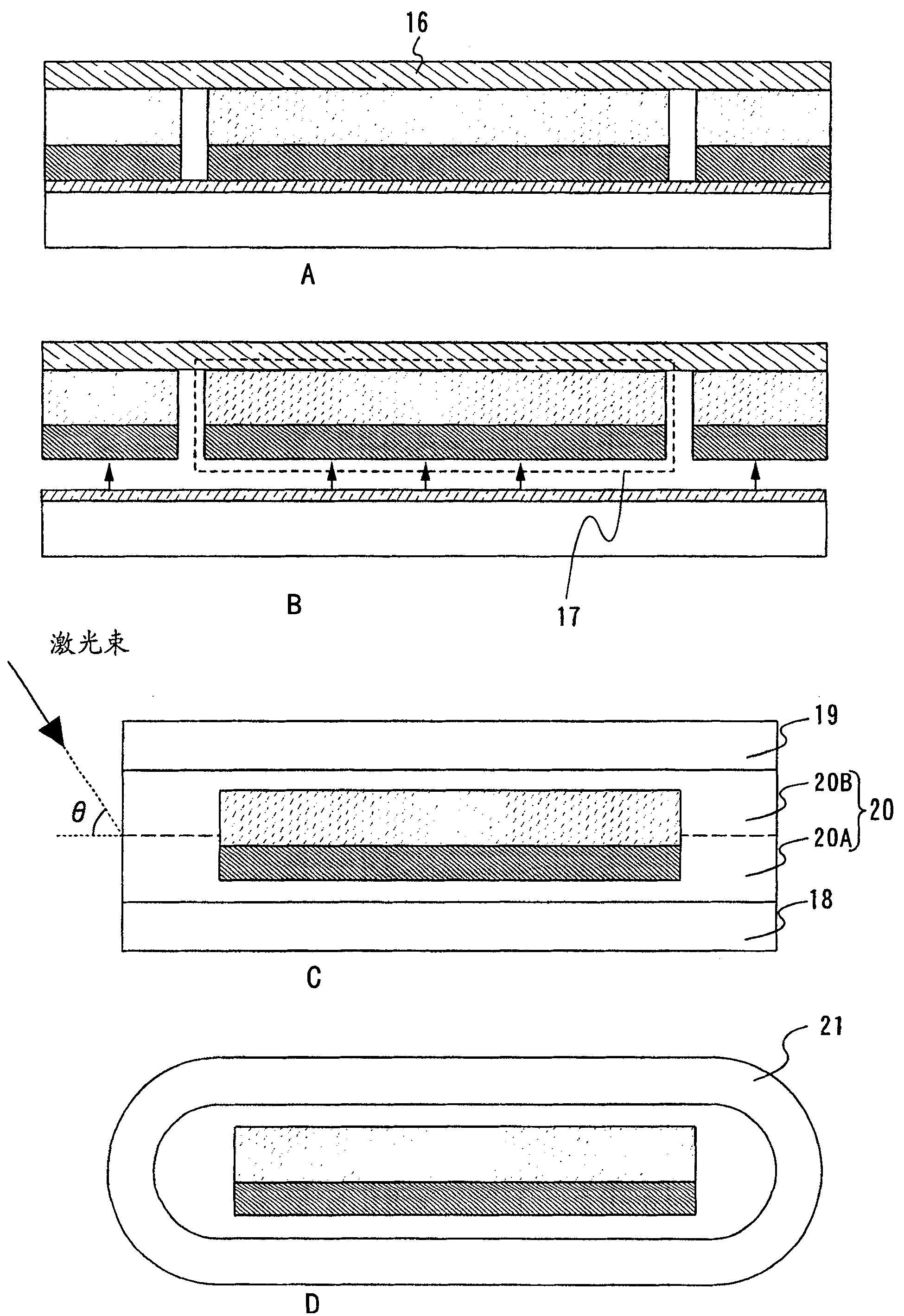
接下来,在从衬底11剥离的叠层体17的一方表面上设置第一叠层膜(也称作层压膜)。第一叠层膜是在粘合到叠层体17中设置有元件层13一侧的面之后,通过进行加热处理和加压处理的单方或双方来设置。Next, a first laminated film (also referred to as a laminated film) is provided on one surface of the
接下来,在叠层体17的另一方表面(与设置有第一叠层膜的面相反的面,即叠层体17中设置有绝缘膜14一侧的面)上设置第二叠层膜。在此情况下,为了形成更薄的半导体器件,优选在除去膜16之后另外设置第二叠层膜。此外,作为第二叠层膜优选使用具有与第一叠层膜相同的结构的膜。Next, a second laminated film is provided on the other surface of the laminated body 17 (the surface opposite to the surface provided with the first laminated film, that is, the surface of the
第一叠层膜及第二叠层膜至少一方表面具有粘合剂层,并且该粘合剂层与叠层体17互相接触着贴合即可。此外,第一叠层膜及第二叠层膜由基材(基膜)和粘合剂层层叠的膜构成。在本实施方式中,第一叠层膜具有第一基材18及第一粘合剂层20A,第二叠层膜具有第二基材19及第二粘合剂层20B。并且,在叠层体17的侧面附近,第一叠层膜所具有的第一粘合剂层20A与第二叠层膜所具有的第二粘合剂层20B互相贴合,构成粘合剂层20(图2C)。At least one surface of the first laminated film and the second laminated film has an adhesive layer, and the adhesive layer and the
作为基材(基膜),使用其熔点至少比用作粘合剂的材料高的材料即可,根据目的适当选用。也就是说,除了单层的膜以外,还可以适当地层叠性质互不相同的膜而构成基材。具体而言,作为可以用作基材的膜,可以举出聚乙烯、聚对苯二甲酸乙二醇酯(PET)、聚萘二甲酸乙二醇酯(PEN)、尼龙、乙烯-乙烯醇共聚物膜(EVOH)、聚丙烯、聚苯乙烯、AS树脂、ABS树脂(由丙烯腈、丁二烯、以及苯乙烯这三种聚合而成的树脂)、甲基丙烯树脂(也称作丙烯酸)、聚氯乙烯、聚缩醛、聚酰胺、聚碳酸酯、变性聚亚苯基醚、聚对苯二甲酸丁二醇酯(PBT)、聚砜、聚醚砜(PES)、聚苯硫醚、聚酰胺-酰亚胺、聚甲基戊烯、酚醛树脂、尿素树脂、三聚氰胺树脂、环氧树脂、邻苯二甲酸二烯丙酯树脂、不饱和聚酯树脂、聚酰亚胺、以及聚氨基甲酸乙酯等材料;纤维材料(例如纸);实施了抗静电加工的膜(抗静电膜)等。As the base material (base film), a material whose melting point is at least higher than that of the material used as the binder may be used, and it is appropriately selected according to the purpose. That is, in addition to a single-layer film, films having different properties may be appropriately laminated to constitute the substrate. Specifically, examples of films that can be used as substrates include polyethylene, polyethylene terephthalate (PET), polyethylene naphthalate (PEN), nylon, ethylene-vinyl alcohol Copolymer film (EVOH), polypropylene, polystyrene, AS resin, ABS resin (resin made by polymerizing acrylonitrile, butadiene, and styrene), methacrylic resin (also called acrylic acid) ), polyvinyl chloride, polyacetal, polyamide, polycarbonate, denatured polyphenylene ether, polybutylene terephthalate (PBT), polysulfone, polyethersulfone (PES), polyphenylene sulfide Ether, polyamide-imide, polymethylpentene, phenolic resin, urea resin, melamine resin, epoxy resin, diallyl phthalate resin, unsaturated polyester resin, polyimide, and Materials such as polyurethane; fiber materials (such as paper); antistatically processed films (antistatic films), etc.
作为实施了抗静电加工的膜,可以举出在树脂内分散有抗静电材料的膜、贴有抗静电材料的膜等。贴有抗静电材料的膜既可以是在作为基材的膜中一方表面上贴有抗静电材料的膜,也可以在两个表面上贴有抗静电材料的膜。此外,其中一方表面上贴有抗静电材料的膜可以在该膜的外侧贴有该抗静电材料,优选在该膜的内侧贴有该抗静电材料。此外,该抗静电材料可以贴附到该膜的整个表面或部分表面上。作为抗静电材料可以使用铝等金属、含铟和锡的氧化物(氧化铟锡;ITO)、或两性表面活性剂金属盐、咪唑啉型两性表面活性剂、含有以羧基和季铵碱基作为侧链的交联共聚物高分子的树脂材料等。通过使用抗静电膜作为第一基材18和第二基材19,可以防止外部静电对集成电路造成不良影响。Examples of the film subjected to antistatic processing include a film in which an antistatic material is dispersed in a resin, a film in which an antistatic material is pasted, and the like. The film with an antistatic material may be a film with an antistatic material on one surface of the film as a base material, or a film with an antistatic material on both surfaces. In addition, the antistatic material can be pasted on the outside of the film, and the antistatic material is preferably pasted on the inside of the film. In addition, the antistatic material may be attached to the entire surface or part of the surface of the film. Metals such as aluminum, oxides containing indium and tin (indium tin oxide; ITO), or amphoteric surfactant metal salts, imidazoline type amphoteric surfactants, containing carboxyl and quaternary ammonium bases can be used as antistatic materials. Side chain cross-linked copolymer polymer resin materials, etc. By using an antistatic film as the
作为粘合剂,使用熔点至少比用作基材的材料低的材料即可。例如,可以使用以聚乙烯类树脂、聚酯类树脂、乙烯-醋酸乙烯酯(EVA)等热可塑性树脂、热固化树脂、紫外线固化树脂等为主要成分的材料。此外,在进行加热处理和加压处理而将膜粘附到元件层时,通过加热处理熔化设置于叠层膜的最外表面的粘合剂层或设置于叠层膜的最外层的层(不是粘合剂层),随后通过施加压力而粘附。As the binder, a material having a melting point at least lower than that of the material used as the base material may be used. For example, materials mainly composed of polyethylene-based resins, polyester-based resins, thermoplastic resins such as ethylene-vinyl acetate (EVA), thermosetting resins, and ultraviolet-ray curing resins can be used. In addition, when heat treatment and pressure treatment are performed to adhere the film to the element layer, the adhesive layer provided on the outermost surface of the laminated film or the layer provided on the outermost layer of the laminated film is melted by heat treatment (not an adhesive layer), which are then adhered by applying pressure.
此外,为了进一步防止水分侵入到最终形成的半导体器件(叠层体17)内部,优选在基材和粘合剂层之间涂覆二氧化硅(硅土)粉末。通过涂覆,可以进一步提高在高温、高湿度环境下的耐湿性。此外,出于相同目的,也可以通过在基材和粘合剂层之间设置如下叠层膜,进一步防止水分等侵入到最终形成的半导体器件(叠层体17)内部,该叠层膜是通过CVD法、溅射法、蒸发淀积法等形成以氧化硅、氮化硅、含有氧的氮化硅、含有氮的氧化硅、或陶瓷(例如是氧化铝)为主要成分的膜而形成的。此外,为了提高最终形成的半导体器件的物理强度,也可以通过CVD法、溅射法、蒸发淀积法等将以碳为主要成分的材料(例如类金刚石碳)涂覆到与设置有粘合剂层的基材的表面相反的表面(暴露于外部的一侧)。此外,也可以涂覆混合二氧化硅(硅土)的粉末、含氧的氮化硅、或含氮的氧化硅和以碳为主要成分的材料而成的材料。可以针对第一叠层膜和第二叠层膜的单方或双方实施这些处理。In addition, in order to further prevent intrusion of moisture into the inside of the finally formed semiconductor device (laminated body 17), it is preferable to coat silicon dioxide (silica) powder between the base material and the adhesive layer. By coating, the moisture resistance in high temperature and high humidity environments can be further improved. In addition, for the same purpose, it is also possible to further prevent intrusion of moisture or the like into the inside of the finally formed semiconductor device (laminate 17) by providing a laminated film between the base material and the adhesive layer, the laminated film being Formed by forming a film mainly composed of silicon oxide, silicon nitride, silicon nitride containing oxygen, silicon oxide containing nitrogen, or ceramics (such as aluminum oxide) by CVD method, sputtering method, evaporation deposition method, etc. of. In addition, in order to improve the physical strength of the final formed semiconductor device, it is also possible to apply a material (such as diamond-like carbon) with carbon as the main component to the bonding surface by CVD, sputtering, evaporation, etc. The surface opposite to the surface of the substrate of the agent layer (the side exposed to the outside). In addition, a material obtained by mixing powder of silicon dioxide (silica), silicon nitride containing oxygen, or silicon oxide containing nitrogen, and a material mainly composed of carbon may be applied. These treatments may be performed on one or both of the first laminated film and the second laminated film.
接下来,使用切断装置来切断第一叠层膜和第二叠层膜。切断装置相当于切割器(dicer)、激光、线锯等。通过该切断工序,可以获得如图2C所示的结构,即叠层体17的周围由粘合剂层20覆盖,并且粘合剂层20的双面由第一基材18及第二基材19密封。此时,粘合剂层20的侧面处于暴露于外部的状态。Next, the first laminated film and the second laminated film are cut using a cutting device. The cutting device corresponds to a dicer, a laser, a wire saw, or the like. Through this cutting process, the structure shown in Figure 2C can be obtained, that is, the periphery of the
接下来,用激光束照射第一叠层膜及第二叠层膜的切断面(侧面)(图2C)。通过照射激光束所获得的结构是,第一基材18和第二基材19熔化粘合而成为第三基材21,粘合剂层20的切断面(侧面)由第三基材21密封。此时,第一基材18和第二基材19的至少一方由激光束照射熔化而互相熔和粘连即可,但优选是第一基材18和第二基材19的双方熔化而互相熔和粘连。最终形成由第三基材21覆盖粘合剂层20的切断面(侧面)的半导体器件(图2D)。图2D所示的第三基材21的形状是示意性形状,并不局限于该形状。Next, the cut surfaces (side surfaces) of the first laminated film and the second laminated film are irradiated with laser beams ( FIG. 2C ). The structure obtained by irradiating the laser beam is that the
用于上述工序的激光束的条件没有特别的限制,只要是能够使第一基材18与第二基材19熔化而粘合的条件即可。例如,可以使用CO2激光。此外,也可以使用波长为100至380nm(UV)的激光(例如,Nd:YVO4激光的第三高次谐波等固体激光)。如果使用紫外线激光,采用功率密度为2至3W/cm2(包括2W/cm2和3W/cm2)即可。此外,激光束的扫描速度采用0.5至1.5mm/sec。(包括0.5mm/sec和1.5mm/sec)即可。激光束的扫描速度是激光束相对于第一叠层膜及第二叠层膜的切断面(侧面)相对移动的速度。此外,照射的激光束的射束点的形状没有特别的限制,可以采用圆形、椭形、或长方形等。The conditions of the laser beam used in the above steps are not particularly limited, as long as the
接下来说明激光束的照射角度。由对第一叠层膜及第二叠层膜的切断面(侧面)照射激光束的方向和对第一叠层膜及第二叠层膜的切断面(侧面)的垂线(或者对于叠层体17的一方表面平行的面)形成的棱角,即激光束对于第一叠层膜及第二叠层膜的切断面(侧面)的入射角(θ;0°≤θ≤90°)优选为如图2C所示那样对于第一叠层膜及第二叠层膜的切断面(侧面)倾斜地照射激光束。当θ小于30°时,如果第一叠层膜及第二叠层膜不能充分吸收激光,则设置在叠层体17内部的元件有可能被破坏,因此θ优选为30°或更大。此外,当θ大于80°时,粘合剂层20的切断面难以密封,因此θ优选为80°或更小。根据如上理由,θ优选为30至80°(包括30°和80°)(更优选为45至65°;包括45度和65°)。但是,也可以相对于第一叠层膜及第二叠层膜的切断面(侧面)平行(也就是说θ为90°)地照射激光束。在本实施方式中采用照射激光束的方法,但也可以采用其他方法,只要第一基材18及第二基材19能够密封粘合剂层20即可。Next, the irradiation angle of the laser beam will be described. From the direction in which the laser beam is irradiated to the cut surfaces (side surfaces) of the first laminated film and the second laminated film and the perpendicular line to the cut surfaces (side surfaces) of the first laminated film and the second laminated film (or for the laminated film The angle formed by the plane parallel to one surface of the
如上述那样,在使用具有粘合剂层的第一及第二叠层膜密封叠层体17之后,通过用激光束照射暴露出来的第一叠层膜及第二叠层膜的切断面(侧面),第一基材18及第二基材19被熔化粘合。通过采用粘合剂层的切断面(侧面)不暴露于外部的结构,可以抑制水分或造成污染的物质侵入到半导体器件的内部,由此能够获得具有优良的化学强度、物理强度及耐环境性的半导体器件。此外,其结果是,可以提高半导体器件的成品率并且降低半导体器件的成本。此外,在本实施方式中制造的半导体器件是从厚度大因而通常不具备柔软性的衬底上剥离下来而形成的。由此,可以获得具有柔性的半导体器件,从而可以将本半导体器件设置到各种场所,如物品的曲面部分等。As described above, after the
实施方式2Embodiment 2
在本实施方式中说明与实施方式1中所说明的方法不同的半导体器件的制造方法。In this embodiment mode, a method of manufacturing a semiconductor device different from the method described in
首先,在衬底11的一方表面上形成设置有多个具有薄膜晶体管等元件的集成电路的层13(以下,称作元件层13)(图3A)。在本说明书中,衬底11的一方表面指的是设置有元件层13一侧的表面。衬底11和元件层13的材料及形成方法等在实施方式1中已经说明,所以下面详细说明此后的工序。First, a layer 13 (hereinafter referred to as an element layer 13 ) in which a plurality of integrated circuits including elements such as thin film transistors are provided is formed on one surface of a substrate 11 ( FIG. 3A ). In this specification, one surface of the
在担心元件层13受到来自衬底11的杂质等污染的情况下,优选在衬底11和元件层13之间形成基底膜。作为基底膜,可以适当地采用在实施方式1中所说明的膜。When there is concern about contamination of the
此外,用于确保元件层13的强度的保护层可以覆盖着元件层13形成绝缘膜。该绝缘膜优选是覆盖着元件层13的整个面形成,但并不一定需要在其整个面上形成,也可以有选择地形成。绝缘膜的材料可以使用含有DLC(类金刚石碳)等的碳膜、含氮的氧化硅膜、含氧的氮化硅膜、由有机材料构成的膜(例如,环氧等的树脂材料)。形成绝缘膜的方法可以使用溅射法、等离子体CVD法等的各种CVD法、旋涂法、液滴喷射法、或印刷法等。In addition, a protective layer for securing the strength of the
接下来,在元件层13上贴附膜26。接着,使用衬底固定工具(框子)51将膜26设置到吸附装置(图3A)。吸附装置由例如多孔吸盘52和载物台53构成。此外,多孔吸盘52由多孔材料构成,并具有真空吸盘机构。为了防止衬底固定工具本身被磨削、抛光,设置的膜26要使衬底11的一方表面(设置有膜26一侧的面)高于衬底固定工具51的一方表面。Next, the
膜26具有如下作用:在之后磨削、抛光衬底时固定衬底;保护元件层13;以及在从膜26分离出半导体器件时确保半导体器件之间的空隙。作为起到这种作用的膜,优选使用扩张膜。此外,也可以使用将保护元件层13的膜和扩张膜层叠而成的膜。此外,作为膜26优选使用具有如下性质的膜,即在通常状态下具有高粘合力,但当照射光时该粘合力降低。例如,优选使用通过照射紫外光而其粘合力降低的UV胶带。The
接下来,用磨削工具41磨削衬底11的另一方表面。此时,将衬底11的厚度磨削至100μm或更薄。一般而言,在该磨削工序中,通过使固定有衬底11的载物台53和磨削工具41的一方或双方旋转来磨削衬底11的另一方表面。磨削工具41相当于例如磨刀石。在本说明书中,衬底11的另一方表面指的是与设置有元件层13一侧的面相反的面,是由磨削工具41磨削的那一侧的面。为了除去磨削工序产生的尘灰,必要时可以进行清洗。此时,使因清洗而产生的水滴自然干燥或用干燥方法进行干燥。干燥方法的具体例子有:使衬底11旋转的方法;用鼓风机向衬底11吹出空气(大气)或稀有气体等气体的方法。Next, the other surface of the
接下来,用抛光工具42抛光已经被磨削的衬底11的另一方表面(图3B)。将衬底11抛光到厚度小于100μm即可,但优选为2μm至50μm(包括2μm和50μm)(更优选为4μm至30μm(包括4μm和30μm))。通过这样磨削、抛光衬底11,衬底11变得具有柔性,从而可以不使用从衬底11剥离元件层的方法而制造具有柔性的半导体器件。该抛光工序与上述磨削工序相同,通过使固定有衬底11的载物台53和抛光工具42的一方或双方旋转,抛光衬底11的另一方表面。抛光工具42相当于例如涂布有抛光粒(例如氧化铈等)的抛光垫。必要时,为了除去因抛光工序而产生的尘灰,也可以进行清洗。在此情况下,使因清洗而产生的水滴自然干燥或用干燥方法干燥。干燥方法的具体例子如下:使衬底11旋转的方法;用鼓风机向衬底11吹出空气(大气)或稀有气体等气体的方法。Next, the other surface of the
接下来,从吸附装置分离膜26。接着,使用切断装置43切断衬底11和元件层13,但不要切断膜26(图3C)。此时,切断集成电路彼此的界线(集成电路之间),以使元件层13具有的多个集成电路相互分离。此外,切断设置在元件层13的绝缘膜,但不要切断设置在元件层13的元件。经过该切断工序形成多个叠层体27,其具备薄型化了的衬底11和设置有集成电路的层13。切断装置相当于切割器、激光、线锯。Next, the
接下来,通过拉伸膜26在叠层体27之间形成空隙(图4A)。此时,优选向膜26的表面方向均匀地伸展(向表面方向均匀地拉伸),以使叠层体27之间的各个空隙均匀。接下来,向膜26照射光。如果膜26是UV胶带则照射紫外光。通过向膜26照射光,使膜26的粘合力降低,从而膜26和叠层体27之间的紧密性也降低。这样,达到可以用物理方法从膜26分离出叠层体27的状态。Next, voids are formed between the
在上述工序中,在拉伸膜26的工序之后执行对膜26照射光的工序,然而本发明不局限于该顺序。也可以在对膜26照射光之后执行拉伸膜26的工序。In the above-described process, the process of irradiating the
接下来,进行叠层体27的密封处理。密封处理包括两种方法。首先说明第一方法。Next, the sealing process of the
在第一方法中,首先用转移设备44从膜26分离出叠层体27(图4B)。接着,用转移设备44将叠层体27设置到第一叠层膜61上,以便将叠层体27的一方表面粘附到第一叠层膜61。作为转移设备44,具体地包括接触转移方法例如用销子的上举、用机械臂的拾取、用真空机构的真空吸附等、以及无接触转移方法等例如使用磁力、空气压力、静电力作为吸附力或浮力的方法。In the first method, the laminate 27 is first separated from the
接下来,将叠层体27的另一方表面粘附到第二叠层膜62(图4C)。该工序是利用粘合装置(以下称作层压装置)完成的,该层压装置包括具有加热工具和加压工具的一方或双方的第一滚筒45和卷绕有第二叠层膜62并且将该第二叠层膜62供给给第一滚筒45的第二滚筒46。Next, the other surface of the
设置有多个叠层体27的第一叠层膜61由搬送机47依次搬送。此外,第一滚筒45及第二滚筒46分别依次旋转,连续地执行叠层体27的密封处理。在此进行的密封处理相当于如下处理:粘附有叠层体27的第一叠层膜61经过第一滚筒45和搬送机47之间时进行加压处理和加热处理的一方或双方,以将第一叠层膜61及第二叠层膜62粘附到叠层体27。在由第一滚筒45和搬送机47进行加热处理的情况下,第一滚筒45具有相当于电热线的加热器或油等的加热装置。此外,在进行加热处理和加压处理的双方的情况下,通过进行加热处理熔化设置在叠层膜的最外表面上的粘合剂层,然后施加压力而粘合。搬送机47相当于传送带、多个滚轮或机器手臂。The first
用于密封的第一叠层膜61具有第一基材和第一粘合剂层,第二叠层膜62具有第二基材和第二粘合剂层。作为基材及粘合剂层,可以应用在实施方式1中所说明的材料。此外,第一叠层膜61及第二叠层膜62由热压合(加热处理和加压处理)粘附到叠层体27。The first
接下来,用切断装置48切断第一叠层膜61及第二叠层膜62(图4D)。切断装置48相当于切割器、激光、线锯等。经过该切断工序,就可以获得叠层体27的周围由粘合剂层覆盖并且粘合剂层的双面由第一基材及第二基材密封的结构。此时,粘合剂层的侧面暴露于外部。Next, the first
接下来,用激光束照射粘合剂层暴露出来的面(粘合剂层的侧面)。通过照射激光束,第一基材和第二基材熔化粘合,形成第三基材。这样就形成了粘合剂层的侧面也被第三基材覆盖的半导体器件。Next, the exposed face of the adhesive layer (the side of the adhesive layer) was irradiated with a laser beam. By irradiating the laser beam, the first base material and the second base material are melted and bonded to form the third base material. This forms a semiconductor device in which the sides of the adhesive layer are also covered with the third substrate.
上述工序中使用的激光束的条件没有特别的限制,只要是可以使第一基材和第二基材熔化而粘合的条件即可。例如,可以使用CO2激光。此外,也可以使用波长为100至380nm(UV)的固体激光(例如,Nd:YVO4激光)。对于粘合剂层20的侧面的激光束照射角度(θ)可以相对于粘合剂层的侧面倾斜(θ优选为10至60°(包括10°和60°),更优选为25至45°(包括25°和45°))照射激光束,也可以相对于粘合剂层的侧面平行(也就是说,θ为90°)照射激光束。特别在如上述那样使用激光切断第一叠层膜61及第二叠层膜62的情况下,通过适当地设定激光的条件,也可以采用在切断的同时利用第一基材及第二基材将粘合剂层密封起来的结构。The conditions of the laser beam used in the above steps are not particularly limited, as long as the first base material and the second base material can be melted and bonded together. For example, a CO2 laser can be used. In addition, a solid-state laser (for example, Nd:YVO 4 laser) having a wavelength of 100 to 380 nm (UV) can also be used. The laser beam irradiation angle (θ) to the side of the
下面说明第二方法。The second method will be described below.
首先,对膜26照射光,以降低膜26和叠层体27之间的紧密性。接着,覆盖着叠层体27的一方表面设置第一叠层膜61(图5A)。接着,用加热手段49加热第一叠层膜61,以将叠层体27的一方表面粘附到第一叠层膜61。接着,从膜26分离出叠层体27(图5B)。First, the
在第二方法中,在对膜26照射光后,覆盖着叠层体27的一方表面设置第一叠层膜61。但本发明并不局限于该顺序。例如,也可以在覆盖着叠层体27的一方表面设置第一叠层膜61、然后加热该第一叠层膜61之后,对膜26照射光。In the second method, after the
接下来,将叠层体27的另一方表面粘附到第二叠层膜62。接着,切断第一叠层膜61和第二叠层膜62。切断装置48相当于切割器、激光、线锯等。通过该切断工序,就可以获得叠层体27的周围由粘合剂层覆盖并且粘合剂层的双面由第一基材及第二基材密封的结构。此时,粘合剂层的侧面暴露于外部。Next, the other surface of the
接下来,用激光束照射粘合剂层暴露出来的面(粘合剂层的侧面)。通过照射激光束,第一基材和第二基材熔化粘合,形成第三基材。这样,就形成了粘合剂层的侧面也由第三基材覆盖的半导体器件。Next, the exposed face of the adhesive layer (the side of the adhesive layer) was irradiated with a laser beam. By irradiating the laser beam, the first base material and the second base material are melted and bonded to form the third base material. In this way, a semiconductor device is formed in which the sides of the adhesive layer are also covered with the third base material.
用于上述工序的激光束的条件没有特别的限制,只要是可以使第一基材和第二基材熔化而粘合的条件即可。例如,可以使用CO2激光。此外,也可以使用波长为100至380nm(UV)的固体激光(例如,Nd:YVO4激光)。对于粘合剂层20的侧面的激光束照射角度(θ)可以相对于粘合剂层的侧面倾斜(θ优选为10至60°(包括10°和60°),更优选为倾斜25至45°(包括25°和45°))照射激光束,然而也可以相对于粘合剂层的侧面平行(也就是说,θ为90°)照射激光束。特别在使用激光切断上述第一叠层膜61及第二叠层膜62的情况下,通过适当地设定激光的条件,也可以采用在切断的同时利用第一基材及第二基材将粘合剂层密封起来的结构。The conditions of the laser beam used in the above steps are not particularly limited, as long as the first base material and the second base material can be melted and bonded together. For example, a CO2 laser can be used. In addition, a solid-state laser (for example, Nd:YVO 4 laser) having a wavelength of 100 to 380 nm (UV) can also be used. The laser beam irradiation angle (θ) for the side of the
通过上述工序而完成的半导体器件可以抑制水分或造成污染的物质侵入到半导体器件的内部,并且具有优良的化学强度、物理强度及耐环境性。此外,其结果是,可以提高半导体器件的成品率并降低半导体器件的成本。此外,由于衬底的厚度薄,所以可以将本半导体器件设置在例如物品的曲面部分等各种场所。此外,由于衬底的厚度薄,所以半导体器件整体的厚度也变薄,即使将本半导体器件安装到其他物体上也不会降低其设计性。The semiconductor device completed through the above steps can suppress intrusion of moisture or polluting substances into the interior of the semiconductor device, and has excellent chemical strength, physical strength, and environmental resistance. Furthermore, as a result, the yield of semiconductor devices can be improved and the cost of semiconductor devices can be reduced. In addition, since the thickness of the substrate is thin, the present semiconductor device can be installed in various places such as curved surface portions of articles. In addition, since the thickness of the substrate is thin, the thickness of the semiconductor device as a whole is also reduced, and even if the semiconductor device is mounted on other objects, the designability thereof is not deteriorated.
本实施方式可以与上述实施方式进行自由组合。也就是说,本实施方式可以采用上述实施方式所示的材料和形成方法,并且上述实施方式可以采用本实施方式所示的材料和形成方法。This embodiment mode can be freely combined with the above-mentioned embodiment modes. That is to say, this embodiment can employ the materials and forming methods shown in the above-mentioned embodiments, and the above-mentioned embodiments can employ the materials and forming methods shown in this embodiment.
实施例1Example 1
在本实施例中,参照附图说明包含薄膜晶体管和天线的半导体器件的制造方法。特别地,本实施例将详细地说明元件层的结构。In this embodiment, a method of manufacturing a semiconductor device including a thin film transistor and an antenna will be described with reference to the drawings. In particular, this embodiment will describe the structure of the element layer in detail.
首先,在衬底701上形成剥离层702(图6A)。接着,在剥离层702上形成基底膜703(图6B)。由于衬底701、剥离层702和基底膜703可以采用实施方式1所说明的材料和形成方法,所以在此省略其说明。下面说明在基底膜703上形成元件层的工序。本发明可以采用不设置基底膜703的结构。First, a
首先,在基底膜703上形成非晶半导体膜704(例如,以非晶硅为主要成分的膜)(图6C)。非晶半导体膜704通过使用溅射法或等离子体CVD法等的各种CVD法形成为25至200nm(优选为30至150nm)的厚度。接着,将非晶半导体膜704晶化,以形成结晶半导体膜。晶化的方法可以使用激光晶化法、使用RTA或退火炉的热晶化法、使用促进晶化的金属元素的热晶化法、以及组合使用促进晶化的金属元素的热晶化法和激光晶化法的方法等。然后,将所得的结晶半导体膜加工成所希望的形状,以形成结晶半导体膜706至710(图7A)。基底膜703和非晶半导体膜704也可以不暴露于大气中而连续形成。First, an amorphous semiconductor film 704 (for example, a film mainly composed of amorphous silicon) is formed on the base film 703 (FIG. 6C). The
下面,简单说明结晶半导体膜706至710的制造工序的一个例子。将非晶半导体膜晶化的方法,可以举出激光晶化法、使用RTA或退火炉的热晶化法、使用促进晶化的金属元素的热晶化法、以及组合使用促进晶化的金属元素的热晶化法和激光晶化法的方法等。此外,作为其他的晶化方法,也可以施加DC偏压而产生热等离子体并使该热等离子体作用于半导体膜,以进行晶化。Next, an example of the manufacturing process of the crystalline semiconductor films 706 to 710 will be briefly described. The method of crystallizing an amorphous semiconductor film includes a laser crystallization method, a thermal crystallization method using RTA or an annealing furnace, a thermal crystallization method using a metal element that promotes crystallization, and a combination of metal elements that promote crystallization. Element thermal crystallization method and laser crystallization method, etc. In addition, as another crystallization method, a DC bias may be applied to generate thermal plasma, and the thermal plasma may be applied to the semiconductor film for crystallization.
在本实施例中,在使用等离子体CVD法形成膜厚为25至200nm的非晶半导体膜之后,通过加热处理使非晶半导体膜晶化,以形成结晶半导体膜706至710。作为加热处理,可以使用激光加热炉、激光照射,或者可以使用灯光进行照射(以下记为灯退火)以取得激光束。或者,可以组合使用上述方法。In this embodiment, after forming an amorphous semiconductor film with a film thickness of 25 to 200 nm using the plasma CVD method, the amorphous semiconductor film is crystallized by heat treatment to form crystalline semiconductor films 706 to 710 . As the heat treatment, a laser heating furnace, laser irradiation, or irradiation with light (hereinafter referred to as lamp annealing) may be used to obtain a laser beam. Alternatively, the above methods can be used in combination.
在使用激光照射的情况下,可以使用连续振荡型的激光束(CW激光束)或脉冲振荡型的激光束(脉冲激光束)。可用的激光束可以使用从选自如下激光器的一种或多种中获得的激光束:气体激光器如Ar激光器、Kr激光器、受激准分子激光器等;以将Nd、Yb、Cr、Ti、Ho、Er、Tm和Ta中的一种或多种作为掺杂剂添加的单晶YAG、YVO4、镁橄榄石(Mg2SiO4)、YAlO3、GdVO4、或者多晶(陶瓷)YAG、Y2O3、YVO4、YAlO3、GdVO4作为介质的激光器;玻璃激光器;红宝石激光器;变石激光器;Ti:蓝宝石激光器;铜蒸汽激光器;以及金蒸汽激光器。通过照射上述激光的基波以及该基波的第二至第四高次谐波的激光,可以获得大粒径的结晶。例如,可以使用Nd:YVO4激光器(基波为1064nm)的第二高次谐波(532nm)或第三高次谐波(355nm)。Nd:YVO4激光器可以使激光脉冲振荡,也可以使激光连续振荡。在使激光连续振荡的情况下,激光的功率密度约需0.01至100MW/cm2(优选为0.1至10MW/cm2)。并且,以大约10至2000cm/sec的扫描速度进行照射。In the case of using laser irradiation, a continuous oscillation type laser beam (CW laser beam) or a pulse oscillation type laser beam (pulse laser beam) can be used. Available laser beams can use laser beams obtained from one or more selected from the following lasers: gas lasers such as Ar lasers, Kr lasers, excimer lasers, etc.; to convert Nd, Yb, Cr, Ti, Ho , one or more of Er, Tm and Ta added as a dopant single crystal YAG, YVO4, forsterite (Mg 2 SiO 4 ), YAlO 3 , GdVO 4 , or polycrystalline (ceramic) YAG, Y Lasers with 2 O 3 , YVO 4 , YAlO 3 , GdVO 4 as the medium; glass lasers; ruby lasers; alexandrite lasers; Ti:sapphire lasers; copper vapor lasers; and gold vapor lasers. Crystals with large particle diameters can be obtained by irradiating the above-mentioned fundamental wave of laser light and laser light of the second to fourth harmonics of the fundamental wave. For example, the second harmonic (532 nm) or the third harmonic (355 nm) of a Nd:YVO 4 laser (fundamental wave 1064 nm) can be used. Nd:YVO 4 laser can make the laser pulse oscillate, and also can make the laser oscillate continuously. When continuously oscillating the laser light, the power density of the laser light needs to be approximately 0.01 to 100 MW/cm 2 (preferably 0.1 to 10 MW/cm 2 ). And, irradiation is performed at a scanning speed of about 10 to 2000 cm/sec.
以将Nd、Yb、Cr、Ti、Ho、Er、Tm和Ta中的一种或多种作为掺杂剂添加的单晶YAG、YVO4、镁橄榄石(Mg2SiO4)、YAlO3、GdVO4、或者多晶(陶瓷)YAG、Y2O3、YVO4、YAlO3、GdVO4作为介质的激光器;Ar离子激光器;以及Ti:蓝宝石激光器可以产生连续振荡,也可以通过Q开关工作或锁模等以10MHz或更大的振荡频率产生脉冲振荡。当以10MHz或更大的振荡频率使激光振荡时,在半导体膜被激光器熔化到固化的期间中,下一个脉冲照射到半导体膜上。因此,与使用低振荡频率的脉冲激光器的情形不同,因为可以在半导体膜中连续移动固体和液体的界面,所以,能够获得向扫描方向连续成长的结晶粒。Single crystal YAG, YVO4, forsterite (Mg 2 SiO 4 ), YAlO 3 , GdVO with one or more of Nd, Yb, Cr, Ti, Ho, Er, Tm and Ta added as dopants 4. Or polycrystalline (ceramic) YAG, Y 2 O 3 , YVO 4 , YAlO 3 , GdVO 4 lasers as media; Ar ion lasers; and Ti: sapphire lasers can generate continuous oscillation, and can also work through Q switches or lock Mode, etc. generate pulse oscillations at an oscillation frequency of 10MHz or more. When the laser is oscillated at an oscillation frequency of 10 MHz or more, the next pulse is irradiated to the semiconductor film during the period from melting to solidification of the semiconductor film by the laser. Therefore, unlike the case of using a pulsed laser with a low oscillation frequency, since the interface between the solid and the liquid can be continuously moved in the semiconductor film, crystal grains that grow continuously in the scanning direction can be obtained.
当使用如上所述的连续振荡激光器或以10MHz或更大的频率振荡的激光束进行晶化时,可以使被晶化了的半导体膜的表面变得平坦。结果,也可以使后面形成的栅极绝缘膜705薄膜化,并有助于提高栅极绝缘膜的抗压。When crystallization is performed using a continuous oscillation laser as described above or a laser beam oscillating at a frequency of 10 MHz or more, the surface of the crystallized semiconductor film can be flattened. As a result, the thickness of the gate insulating film 705 formed later can also be reduced, contributing to the improvement of the withstand voltage of the gate insulating film.
此外,当使用陶瓷(多晶)作为介质时,可以在短时间内以低成本将介质形成为任意形状。当使用单晶时,通常使用直径为几mm、长度为几十mm的圆柱状的介质。但是,当使用陶瓷时,可以形成更大的介质。Furthermore, when ceramics (polycrystalline) are used as the medium, the medium can be formed into an arbitrary shape in a short time at low cost. When a single crystal is used, a cylindrical medium having a diameter of several mm and a length of several tens of mm is generally used. However, larger media can be formed when ceramics are used.
不管在单晶中或在多晶中都不容易大大改变直接参与发光的介质中Nd和Yb等掺杂剂的浓度,因此,通过增加掺杂剂的浓度来提高激光器的输出有一定的限度。但是,当使用陶瓷时,与单晶相比,可以明显增加介质的尺寸,因此,有可能大幅度提高输出。No matter in single crystal or in polycrystal, it is not easy to greatly change the concentration of dopants such as Nd and Yb in the medium that directly participates in luminescence. Therefore, there is a certain limit to increasing the output of the laser by increasing the concentration of dopants. However, when ceramics are used, the size of the dielectric can be significantly increased compared to single crystals, and therefore, it is possible to greatly increase the output.
再者,当使用陶瓷时,可以容易形成平行六面体形状或长方体形状的介质。使用这种形状的介质使振荡光在介质内部以锯齿形传播,可以使振荡光路变长。因此,增幅变大,可以使激光以高输出振荡。此外,由于从上述形状的介质发射出来的激光束在发射时的截面形状为四角形状,所以,与圆形光束相比,有利于整形为线状光束。通过使用光学系统对如上所述那样发射的激光束进行整形,可以容易获得短边长为1mm或更小、长边长为几mm至几m的线状光束。此外,通过将激发光均匀照射到介质上,使得线状光束的能量沿着长边方向均匀分布。Furthermore, when ceramics are used, a parallelepiped-shaped or rectangular parallelepiped-shaped medium can be easily formed. Using a medium of this shape makes the oscillating light propagate in a zigzag shape inside the medium, which can lengthen the oscillating light path. Therefore, the amplitude becomes large, and the laser can be oscillated with a high output. In addition, since the cross-sectional shape of the laser beam emitted from the medium of the above-mentioned shape is square when emitted, it is more advantageous to shape the laser beam into a linear beam than a circular beam. By shaping the laser beam emitted as described above using an optical system, a linear beam having a short side length of 1 mm or less and a long side length of several mm to several m can be easily obtained. In addition, by uniformly irradiating the excitation light onto the medium, the energy of the linear beam is uniformly distributed along the long-side direction.
通过将上述线状光束照射到半导体膜,可以对半导体膜进行更均匀的加热。当必须均匀加热到线状光束的两端时,只要在其两端配置狭缝并对能量的衰弱部进行遮挡等即可。The semiconductor film can be heated more uniformly by irradiating the above-mentioned linear beam to the semiconductor film. When it is necessary to uniformly heat both ends of the linear beam, it is only necessary to arrange slits at both ends and shield the weakened part of the energy.
使用如上所述那样获得的强度均匀的线状光束对半导体膜进行加热,并且使用该半导体膜制造半导体器件,就能够使该半导体器件的特性良好而均匀。By heating a semiconductor film with the linear beam of uniform intensity obtained as described above, and manufacturing a semiconductor device using the semiconductor film, the characteristics of the semiconductor device can be made good and uniform.
接着,覆盖着结晶半导体膜706至710形成栅极绝缘膜705。可以通过溅射法或等离子体CVD法等的各种CVD法形成栅极绝缘膜705。具体而言,可以使用氧化硅膜(SiOx膜)、氮化硅膜(SiNx膜)、含氮的氧化硅膜(SiOxNy膜)(x>y)(x、y为正整数)、含氧的氮化硅膜(SiNxOy膜)(x>y)(x、y为正整数)形成单层结构,或者将这些膜适当层叠。此外,也可以通过在氧、氮、或含有氧和氮的气体介质中对结晶半导体膜706至710进行高密度等离子体处理,使结晶半导体膜706至710的表面氧化或氮化,形成栅极绝缘膜。与通过CVD法或溅射法等形成的膜相比,进行高密度等离子体处理而形成的栅极绝缘膜具有更均匀的膜厚和膜质,并且通过高密度等离子体处理可以形成更细致的膜。Next, a gate insulating film 705 is formed covering the crystalline semiconductor films 706 to 710 . The gate insulating film 705 can be formed by various CVD methods such as sputtering and plasma CVD. Specifically, a silicon oxide film (SiOx film), a silicon nitride film (SiNx film), a nitrogen-containing silicon oxide film (SiOxNy film) (x>y) (x, y are positive integers), an oxygen-containing A silicon nitride film (SiNxOy film) (x>y) (x, y are positive integers) forms a single-layer structure, or these films are stacked appropriately. In addition, it is also possible to oxidize or nitride the surfaces of the crystalline semiconductor films 706 to 710 by performing high-density plasma treatment on the crystalline semiconductor films 706 to 710 in oxygen, nitrogen, or a gaseous medium containing oxygen and nitrogen to form gate electrodes. insulating film. Compared with films formed by CVD, sputtering, etc., the gate insulating film formed by high-density plasma treatment has a more uniform film thickness and film quality, and can be formed finer by high-density plasma treatment. membrane.
在本说明书中的高密度等离子体处理的特征在于等离子体的电子密度为大于等于1×1011cm-3小于等于1×1013cm-3,并且等离子体的电子温度为大于等于0.5eV小于等于1.5eV。下面,在本说明书中只记为高密度等离子体处理的情况下,该高密度等离子体处理意味着以上述条件来进行等离子体处理。由于等离子体的电子密度虽然很高,但形成在衬底上的被处理物(金属膜)附近的电子温度很低,所以可以防止对衬底的等离子体产生损伤。此外,等离子体的电子密度为高密度的1×1011cm-3或更大,因此,进行氧化处理而形成的氧化物的膜厚均匀性高,并且可以形成细致的膜。此外,等离子体的电子温度为低温度的1.5eV或更小,因此,比起等离子体处理或热氧化法来,可以以更低温度进行氧化处理。例如,即使以比玻璃衬底的应变点温度低100℃以上的温度(典型的是250至550℃)进行等离子体处理,也可以充分地进行等离子体氧化处理。使用微波(2.45GHz)作为形成等离子体的频率。此外,等离子体的电位为小于等于5V的低电位,能够抑制原料分子的过量分解。The high-density plasma treatment in this specification is characterized in that the electron density of the plasma is 1×10 11 cm -3 or more and 1×10 13 cm -3 or less, and the electron temperature of the plasma is 0.5 eV or more and less than Equal to 1.5eV. Hereinafter, when only high-density plasma treatment is described in this specification, this high-density plasma treatment means performing plasma treatment under the above-mentioned conditions. Since the electron density of the plasma is high, the temperature of the electrons formed near the object to be processed (metal film) on the substrate is low, so that damage to the substrate by the plasma can be prevented. In addition, since the electron density of the plasma is as high as 1×10 11 cm −3 or more, the oxide formed by the oxidation treatment has high uniformity in film thickness and can form a fine film. In addition, the electron temperature of plasma is 1.5 eV or less, which is a low temperature, so oxidation treatment can be performed at a lower temperature than plasma treatment or thermal oxidation. For example, even if the plasma treatment is performed at a temperature 100° C. or more lower than the strain point temperature of the glass substrate (typically 250 to 550° C.), the plasma oxidation treatment can be sufficiently performed. Microwaves (2.45 GHz) were used as the frequency for forming plasma. In addition, the potential of the plasma is as low as 5 V or less, and excessive decomposition of raw material molecules can be suppressed.
作为含氧的气体介质,可以使用混合有氧(O2)、二氧化氮(NO2)、或一氧化二氮(N2O)和稀有气体的混合气体、或混合有氧(O2)、二氧化氮(NO2)、或一氧化二氮(N2O)和稀有气体和氢(H2)的混合气体。此外,作为含氮的气体介质,可以使用混合有氮(N2)或氨(NH3)和稀有气体的混合气体、或混合有氮(N2)或氨(NH3)和稀有气体和氢(H2)的混合气体。借助于由高密度等离子体生成的氧基(有时候含有OH基)和氮基(有时候含有NH基),可以使结晶半导体膜706至710的表面氧化或氮化。As the oxygen-containing gas medium, a mixture of oxygen (O 2 ), nitrogen dioxide (NO 2 ), or nitrous oxide (N 2 O) and a rare gas can be used, or a mixture of oxygen (O 2 ) , nitrogen dioxide (NO 2 ), or a mixture of nitrous oxide (N 2 O) and rare gases and hydrogen (H 2 ). In addition, as the nitrogen-containing gas medium, a mixed gas mixed with nitrogen (N 2 ) or ammonia (NH 3 ) and a rare gas, or a mixed gas mixed with nitrogen (N 2 ) or ammonia (NH 3 ) and a rare gas and hydrogen can be used. (H 2 ) mixed gas. The surfaces of the crystalline semiconductor films 706 to 710 can be oxidized or nitrided by means of oxygen groups (sometimes containing OH groups) and nitrogen groups (sometimes containing NH groups) generated by high-density plasma.
在进行高密度等离子体处理而形成栅极绝缘膜705的情况下,在结晶半导体膜706至710上形成1至20nm,典型的为5至10nm的绝缘膜。由于在这种情况下的反应就是固相反应,所以可以使所述绝缘膜和结晶半导体膜706至710之间的界面态密度变得极低。此外,由于将结晶半导体膜706至710直接氧化或氮化,所以可以使所形成的栅极绝缘膜705的厚度的不均匀性极低,达到理想状态。再者,由于在结晶硅的晶界也不发生较强的氧化,所以可以达到非常理想的状态。换言之,通过实施在此说明的高密度等离子体处理而将半导体膜的表面固相氧化,可以形成均一性好且界面态密度低的绝缘膜,而不会引起晶界上的异常氧化反应。In the case of forming the gate insulating film 705 by high-density plasma treatment, an insulating film of 1 to 20 nm, typically 5 to 10 nm, is formed on the crystalline semiconductor films 706 to 710 . Since the reaction in this case is a solid phase reaction, the interface state density between the insulating film and the crystalline semiconductor films 706 to 710 can be made extremely low. Furthermore, since the crystalline semiconductor films 706 to 710 are directly oxidized or nitrided, the unevenness of the thickness of the formed gate insulating film 705 can be extremely low, ideally. Furthermore, since strong oxidation does not occur at the grain boundaries of crystalline silicon, a very ideal state can be achieved. In other words, by performing the high-density plasma treatment described here to oxidize the surface of the semiconductor film in the solid state, an insulating film with good uniformity and low interface state density can be formed without causing abnormal oxidation reactions at the grain boundaries.
可以仅使用进行高密度等离子体处理而形成的绝缘膜作为栅极绝缘膜705,或者在使用上述绝缘膜的同时,通过利用等离子体或热反应的CVD法堆积层叠氧化硅、包含氧的氮化硅、包含氮的氧化硅等绝缘膜。在任何情况下,包括使用高密度等离子体而形成的绝缘膜作为栅极绝缘膜的一部或全部而形成的晶体管可以降低特性偏差。As the gate insulating film 705, only an insulating film formed by high-density plasma treatment may be used, or, in combination with the above-mentioned insulating film, silicon oxide or nitride containing oxygen may be stacked by CVD using plasma or thermal reaction. Insulating films such as silicon and silicon oxide containing nitrogen. In any case, a transistor formed including an insulating film formed using high-density plasma as part or all of a gate insulating film can reduce characteristic variation.
此外,对非晶半导体膜704照射以连续振荡激光或以大于等于10MHz的频率振荡的激光束,同时沿着一个方向扫描而晶化的结晶半导体膜706至710具有结晶沿着其光束的扫描方向成长的特性。因此,按照沟道长度方向(当形成沟道形成区域时载流子的流动方向)设定扫描方向而配置晶体管,并且通过组合进行高密度等离子体处理而形成的栅极绝缘膜705,能够降低特性偏差,并获得场效应迁移率高的晶体管。In addition, the crystalline semiconductor films 706 to 710 crystallized by irradiating the
接下来,在栅极绝缘膜705上层叠形成第一导电膜和第二导电膜。通过溅射法或等离子体CVD法等的各种CVD法分别形成第一导电膜和第二导电膜即可。在本实施例中,将第一导电膜形成为20至100nm的厚度,将第二导电膜形成为100至400nm的厚度。此外,第一导电膜和第二导电膜可以使用从钽(Ta)、钨(W)、钛(Ti)、钼(Mo)、铝(Al)、铜(Cu)、铬(Cr)、铌(Nb)等之中选出的元素或者以所述元素为主要成分的合金材料或化合物材料来形成。此外,也可以使用以掺杂了磷等的杂质元素的多晶硅为代表的半导体材料来形成第一导电膜和第二导电膜。作为第一导电膜和第二导电膜的组合的例子,可以举出氮化钽(TaN)膜和钨(W)膜;氮化钨(WN)膜和钨膜;氮化钼(MoN)膜和钼(Mo)膜,等等。由于钨和氮化钽具有高耐热性,因此在形成第一导电膜和第二导电膜之后可以进行以热活化为目的的加热处理。此外,可以采用单层结构替代第一导电膜和第二导电膜的双层结构,或者也可以采用三层结构。在采用单层结构或三层结构的情况下,可以自由地选择与上述第一导电膜和第二导电膜相同的材料作为导电膜的材料。Next, a first conductive film and a second conductive film are stacked on the gate insulating film 705 . The first conductive film and the second conductive film may be formed by various CVD methods such as sputtering or plasma CVD. In this embodiment, the first conductive film is formed to a thickness of 20 to 100 nm, and the second conductive film is formed to a thickness of 100 to 400 nm. In addition, the first conductive film and the second conductive film can be made of tantalum (Ta), tungsten (W), titanium (Ti), molybdenum (Mo), aluminum (Al), copper (Cu), chromium (Cr), niobium (Nb) and the like, or an alloy material or a compound material mainly composed of the element. In addition, the first conductive film and the second conductive film may be formed using a semiconductor material typified by polysilicon doped with an impurity element such as phosphorus. Examples of the combination of the first conductive film and the second conductive film include a tantalum nitride (TaN) film and a tungsten (W) film; a tungsten nitride (WN) film and a tungsten film; a molybdenum nitride (MoN) film and molybdenum (Mo) film, etc. Since tungsten and tantalum nitride have high heat resistance, heat treatment for thermal activation can be performed after the formation of the first conductive film and the second conductive film. In addition, a single-layer structure may be adopted instead of the double-layer structure of the first conductive film and the second conductive film, or a three-layer structure may also be used. In the case of adopting a single-layer structure or a three-layer structure, the same material as the above-mentioned first conductive film and second conductive film can be freely selected as the material of the conductive film.
接下来,使用光刻法形成由抗蚀剂构成的掩模,并进行形成栅极和栅极线所需的蚀刻处理,以形成用作栅极的导电膜716至725(以下,在本说明书中有时称为栅极)。Next, a mask made of a resist is formed using a photolithography method, and etching processing required for forming gates and gate lines is performed to form conductive films 716 to 725 serving as gates (hereinafter, in this specification is sometimes referred to as a gate).
接下来,通过光刻法形成由抗蚀剂构成的掩模之后,采用离子掺杂法或者离子注入法将提供N型的杂质元素以低浓度添加到结晶半导体膜706和708至710中,以形成N型杂质区域711和713至715和沟道形成区域780和782至784。可以使用属于周期表第15族的元素作为提供N型的杂质元素,例如使用磷(P)或砷(As)。Next, after forming a mask made of a resist by photolithography, an impurity element providing an N type is added at a low concentration to the crystalline semiconductor films 706 and 708 to 710 by an ion doping method or an ion implantation method to N-type impurity regions 711 and 713 to 715 and
接下来,通过光刻法形成由抗蚀剂构成的掩模。并且,将提供P型的杂质元素添加到结晶半导体膜707中以形成P型杂质区域712和沟道形成区域781。例如,使用硼(B)作为提供P型的杂质元素。关于形成N型杂质区域711和713至715、P型杂质区域712的顺序,像本实施例那样,可以在形成N型杂质区域711和713至715之后形成P型杂质区域712,或者也可以在形成P型杂质区域712之后形成N型杂质区域711和713至715。Next, a mask made of resist is formed by photolithography. Also, an impurity element providing a P type is added to the crystalline semiconductor film 707 to form a P type impurity region 712 and a
接下来,覆盖着栅极绝缘膜705和导电膜716至725形成绝缘膜。该绝缘膜是通过使用溅射法或等离子体CVD法等的各种CVD法以如下的单层或叠层膜形成的:由无机材料如硅、硅的氧化物、或者硅的氮化物等构成的膜、或者由有机材料如有机树脂等构成的膜。接着,通过使用以垂直方向为主体的各向异性蚀刻有选择性地蚀刻绝缘膜,由此形成与导电膜716至725的侧面接触的绝缘膜(也称为侧壁)739至743(图7B)。形成绝缘膜739至743的同时,形成通过蚀刻栅极绝缘膜705而形成的绝缘膜734至738(以下,也可以称作栅极绝缘膜)。绝缘膜739至743用作其后形成LDD(Lightly Doped drain:轻掺杂漏极)区域时的掺杂用掩模。Next, an insulating film is formed covering the gate insulating film 705 and the conductive films 716 to 725 . The insulating film is formed by various CVD methods such as sputtering or plasma CVD as a single-layer or laminated film composed of an inorganic material such as silicon, silicon oxide, or silicon nitride, etc. film, or a film made of organic materials such as organic resins. Next, the insulating films are selectively etched by using anisotropic etching mainly in the vertical direction, thereby forming insulating films (also referred to as side walls) 739 to 743 in contact with the side surfaces of the conductive films 716 to 725 (FIG. 7B ). Simultaneously with the formation of the insulating
接下来,使用由光刻法所形成的由抗蚀剂构成的掩模和绝缘膜739至743作为掩模,将提供N型的杂质元素添加到结晶半导体膜706和708至710中,以形成第一N型杂质区域(也称为LDD区域)727、729、731及733和第二N型杂质区域726、728、730及732。第一N型杂质区域727、729、731及733所含的杂质元素的浓度低于第二N型杂质区域726、728、730及732的杂质元素的浓度。经过上述工序,完成了N型薄膜晶体管744、746至748和P型薄膜晶体管745。Next, using a mask made of a resist formed by photolithography and the insulating
形成LDD区域有下述两种方法。一个方法是,采用两层或更多的叠层结构作为栅极,进行蚀刻或各向异性蚀刻使该栅极成为锥形,并使用构成该栅极的下层的导电膜作为掩模。另一个方法是将侧壁绝缘膜作为掩模。通过前一种方法形成的薄膜晶体管具有这样的结构:与栅极交叠地配置LDD区域且栅极绝缘膜夹在其间。然而,这种结构由于使用使栅极具有锥形的蚀刻或各向异性蚀刻而难以控制LDD区域的宽度,并且,如果蚀刻工序执行不好,则可能无法形成该LDD区域。另一方面,与前一种方法相比,使用侧壁绝缘层作为掩模的后一种方法容易控制LDD区域的宽度,并且可以切实地形成LDD区域。使栅极具有锥形的蚀刻是指将栅极侧面形成为锥形状的蚀刻。There are the following two methods for forming the LDD region. One method is to use a stacked structure of two or more layers as a gate, perform etching or anisotropic etching to tape the gate, and use a conductive film constituting the lower layer of the gate as a mask. Another method is to use a side wall insulating film as a mask. The thin film transistor formed by the former method has a structure in which an LDD region is arranged to overlap a gate with a gate insulating film interposed therebetween. However, this structure makes it difficult to control the width of the LDD region by using etching or anisotropic etching for tapering the gate, and if the etching process is poorly performed, the LDD region may not be formed. On the other hand, compared with the former method, the latter method using the sidewall insulating layer as a mask can easily control the width of the LDD region, and can reliably form the LDD region. The etching for tapering the gate refers to the etching for forming the side surface of the gate in a tapered shape.
除去形成在暴露出来的N型杂质区域726、728、730、732以及P型杂质区域785的表面上的自然氧化膜之后,也可以使用金属膜适当地分别形成硅化物区域。金属膜可以使用镍膜、钛膜、钴膜、铂膜、或者由至少包含所述元素中的两种元素的合金构成的膜等。更具体地,例如使用镍膜作为金属膜,在室温下以成膜电力为500W至1kW且用溅射法形成镍膜之后,进行加热处理形成硅化物区域。加热处理可以使用RTA或退火炉等。此时,通过控制金属膜的膜厚、加热温度、加热时间,可以只使N型杂质区域726、728、730、732以及P型杂质区域785的表面成为硅化物区域,或者也可以使整体表面成为硅化物区域。最后,除去未反应的镍。例如,使用由HC1∶HNO3∶H2O=3∶2∶1构成的蚀刻溶液除去未反应的镍。After removing the natural oxide films formed on the exposed surfaces of the N-
在本实施例中说明了将顶栅极型薄膜晶体管作为薄膜晶体管744至748的例子。然而,当然也可以将底栅极型薄膜晶体管分别作为薄膜晶体管744至748。此外,在本实施例中说明了各薄膜晶体管744至748具有一个沟道形成区域的单栅极结构,但是,也可以采用具有两个沟道形成区域的双栅极(double gate)结构或具有三个沟道形成区域的三栅极(triple gate)结构。或者可以采用在沟道形成区域的上下方配置有两个栅极且其中间夹有栅极绝缘膜的双栅四极型(dual gate)或其他结构。In this embodiment, an example in which top gate type thin film transistors are used as the
此外,作为构成薄膜晶体管744至748的半导体膜的结构,也可以分别采用在本实施例中说明的结构以外的结构。例如,可以分别形成杂质区域(包括源区、漏区、LDD区域),也可以形成P沟道型、N沟道型、或CMOS电路。此外,也可以形成绝缘膜(侧壁)并使其与形成在半导体膜上方或下方的栅极的侧面相接触。In addition, as the structures of the semiconductor films constituting the
通过上述工序完成N型薄膜晶体管744、746至748以及P型薄膜晶体管745之后,可以进行以恢复半导体膜的结晶性或激活添加在半导体膜中的杂质元素为目的的加热处理。After the N-type
接下来,覆盖着薄膜晶体管744至748形成单层或叠层的绝缘膜(图7C)。覆盖薄膜晶体管744至748的绝缘膜是通过SOG法或液滴喷射法等由无机材料如硅的氧化物或硅的氮化物等、有机材料如聚酰亚胺、聚酰胺、苯并环丁烯、丙烯、环氧、硅氧烷等单层或叠层形成的。本说明书中所说的硅氧烷,其骨架结构由硅(Si)和氧(O)的结合构成,并且使用至少包含氢的有机基(例如烷基、芳香烃)作为取代基。此外,取代基也可以使用氟基,或者也可以使用至少包含氢的有机基以及氟基。例如,在覆盖薄膜晶体管744至748的绝缘膜为三层结构的情况下,优选形成以氧化硅为主要成分的膜作为第一层绝缘膜749,形成以树脂为主要成分的膜作为第二层绝缘膜750,以及形成以氮化硅为主要成分的膜作为第三层绝缘膜751。此外,在覆盖薄膜晶体管744至748的绝缘膜为单层结构的情况下,优选形成氮化硅膜或包含氧的氮化硅膜。此时,优选在包含氢的气体介质中对氮化硅膜或包含氧的氮化硅膜进行高密度等离子体处理,使得该氮化硅膜或该包含氧的氮化硅膜的表面包含氢。这是因为在后面执行半导体膜的氢化工序时可以利用上述氢的缘故。或者,可以通过在对衬底进行350至450℃的加热同时在包含氢的气体介质中执行高密度等离子体处理来实施半导体膜的氢化处理。含氢的气体介质可以使用混合有氢(H2)或氨(NH3)和稀有气体(例如氩(Ar))的混合气体。此外,当使用混合有氨(NH3)和稀有气体(例如氩(Ar))的混合气体作为包含氢的气体介质时,可以在将栅极绝缘膜734至738表面氢化的同时将表面氮化。Next, a single-layer or stacked-layer insulating film is formed covering the
优选在形成绝缘膜749至751之前或在形成绝缘膜749至751中的一个或者多个薄膜之后,实施加热处理,目的是恢复半导体膜的结晶性,激活添加到半导体膜中的杂质元素,或者氢化半导体膜。作为加热处理,优选采用热退火、使用激光的方法、RTA法等。例如,在以激活杂质元素为目的时,只要实施500℃或更高温度的热退火即可。此外,在以氢化半导体膜为目的时,只要实施350至450℃的热退火即可。Preferably, before forming the insulating
接下来,使用光刻法蚀刻绝缘膜749至751,由此形成暴露出来的N型杂质区域726、728、730、732以及P型杂质区域785的接触孔。接着,形成导电膜以填充接触孔,并通过对该导电膜进行图案加工以形成用作源极布线或漏极布线的导电膜752至761。Next, the insulating
导电膜752至761是通过溅射法或等离子体CVD法等的各种CVD法使用以铝(Al)为主要成分的导电膜形成的。以铝为主要成分的导电膜相当于例如以铝为主要成分并包含镍的材料,或者以铝为主要成分并包含镍、以及碳和硅中的单方或双方的合金材料。由于以铝为主要成分的导电膜一般具有耐热性劣势,所以优选采用阻挡膜夹住以铝为主要成分的导电膜的上下结构。阻挡膜是指具有抑制以铝为主要成分的导电膜的小丘(hillock)或改善其耐热性能的膜。具有这种功能的材料可以举出由铬、钽、钨、钼、钛、硅、镍或它们的氮化物构成的材料。The
作为导电膜752至761的结构的一例,可以举出将钛膜、铝膜、钛膜从衬底一侧按此顺序层叠而形成的结构。由于钛是高还原性元素,所以即使在结晶半导体膜上产生了较薄的自然氧化膜,也可以将该自然氧化膜还原并获得与结晶半导体膜之间的良好接触。此外,对形成在结晶半导体膜和铝膜之间的钛膜,优选在含氮的气体介质中执行高密度等离子体处理,使其表面氮化。作为含氮的气体介质,可以使用混合有N2或NH3和稀有气体的混合气体,或者混合有N2或NH3、稀有气体、以及H2的混合气体。通过将钛膜的表面氮化,可以防止在之后进行的加热处理工序等中使钛和铝合金化,并防止铝经过钛膜扩散到结晶半导体膜中。在此虽然说明了使用钛膜夹住铝膜的例子,但是代替钛膜而使用铬膜、钨膜等的情形也与上述相同。更优选地,使用多室装置在不暴露于大气的条件下连续地实施钛膜成膜、钛膜表面氮化处理、铝膜成膜、钛膜成膜。An example of the structure of the
接下来,覆盖着导电膜752至761形成绝缘膜762(图8A)。绝缘膜762是使用SOG法、液滴喷射法等由无机材料或有机材料以单层或叠层形成的。在本实施例中,绝缘膜762形成为0.75至3μm的厚度。Next, an insulating
接下来,使用光刻法蚀刻绝缘膜762形成使导电膜761暴露出来的接触孔。接着,形成导电膜763以填充绝缘膜762的上面和接触孔。由于该导电膜763起着天线的作用,因此,下面有时候将该导电膜763记作天线。导电膜763并不限于单层结构,可以是叠层结构。Next, the insulating
下面说明用作天线的导电膜763的形状。在具有天线(导电膜763)并能够进行非接触数据收发的半导体器件(RFID标签)中,信号传输方式可以采用电磁耦合方式、电磁感应方式或微波方式。只要实施者可以根据使用用途适当地选择传输方式,并且可以根据传输方式适当地设置最合适的天线。Next, the shape of the
例如,当应用电磁耦合方式或电磁感应方式(例如13.56MHz带)作为半导体器件中的信号传输方式时,为了利用磁场密度变化引起的电磁感应,采用环状(例如环形天线)或螺旋状导电膜作天线。For example, when applying an electromagnetic coupling method or an electromagnetic induction method (such as a 13.56 MHz band) as a signal transmission method in a semiconductor device, in order to utilize electromagnetic induction caused by a change in magnetic field density, a loop (such as a loop antenna) or a spiral conductive film is used as an antenna.
当应用微波方式(例如UHF带(860至960MHz带)、2.45GHz带等)作为半导体器件中的信号传输方式时,只要根据用于传输信号的电磁波的波长适当地设定用作天线的导电膜的长度等形状即可。例如,可以将导电膜763形成为线状(例如偶极天线)或者形成为平整的形状(例如贴片天线)。此外,导电膜763的形状不局限于直线状,考虑到电磁波的波长,可以是曲线状、蜿蜒形状,或者是这些形状的组合。When applying a microwave method (such as UHF band (860 to 960MHz band), 2.45GHz band, etc.) The length and other shapes are enough. For example, the
接下来说明用作天线的导电膜763的形成方法及其材料。导电膜763的形成方法可以使用CVD法、溅射法、印刷法如丝网印刷或凹版印刷等、液滴喷射法、点滴法、镀法等。此外,导电膜763的材料可以使用选自铝(Al)、钛(Ti)、银(Ag)、铜(Cu)、金(Au)、铂(Pt)、镍(Ni)、钯(Pd)、钽(Ta)和钼(Mo)中的元素、或者以这些元素为主要成分的合金材料或化合物材料。此外,也可以使用以焊料(优选为不含铅的焊料)为主要成分的微粒子,在这种情况下优选使用粒径20μm或更小的微粒子。焊料的一个优点是成本低。此外,也可以将陶瓷或铁氧体等应用于天线。Next, a method of forming the
例如,当使用丝网印刷法形成导电膜763时,可以通过有选择地印刷如下导电胶来形成导电膜763,在该导电胶中,粒径为几nm至几十μm的导体粒子溶解或分散到有机树脂中。导体粒子可以使用银(Ag)、金(Au)、铜(Cu)、镍(Ni)、铂(Pt)、钯(Pd)、钽(Ta)、钼(Mo)、和钛(Ti)中的任何一个或更多的金属粒子、卤化银的微粒子、或者分散性纳米粒子。此外,导电胶所含的有机树脂可以使用选自用作金属粒子的粘合剂、溶剂、分散剂和覆盖剂的有机树脂中的一个或多个。典型地有环氧树脂、硅树脂等有机树脂。此外,在形成导电膜763时,优选在挤出导电胶之后进行焙烧。例如,当使用以银为主要成分的微粒子(例如粒径1nm或更大至100nm或更小)作为导电胶的材料时,通过在150至300℃的温度范围内焙烧使其固化,可以形成导电膜763。For example, when the
此外,当应用电磁耦合方式或电磁感应方式,并且形成具有天线的半导体器件(RFID标签)并使其接触金属时,优选在所述半导体器件和金属之间形成具有磁导率的磁性材料。在形成具有天线的半导体器件并使其接触金属时,涡电流伴随着磁场的变化而流过金属,并且所述涡电流导致磁场的变化减弱,缩短了通信距离。因此,通过在半导体器件和金属之间形成具有磁导率的磁性材料,可以抑制金属的涡电流和通信距离的缩短。作为磁性材料,可以使用磁导率高且高频损失小的铁氧体或金属薄膜。Furthermore, when applying an electromagnetic coupling method or an electromagnetic induction method, and forming a semiconductor device (RFID tag) having an antenna and bringing it into contact with metal, it is preferable to form a magnetic material having magnetic permeability between the semiconductor device and the metal. When a semiconductor device having an antenna is formed and brought into contact with metal, eddy current flows through the metal accompanying a change in the magnetic field, and the eddy current causes the change in the magnetic field to weaken, shortening the communication distance. Therefore, by forming a magnetic material with magnetic permeability between the semiconductor device and the metal, the eddy current of the metal and the shortening of the communication distance can be suppressed. As the magnetic material, ferrite or metal thin film with high magnetic permeability and low high-frequency loss can be used.
通过上述工序完成元件层。The element layer is completed through the above steps.
在本实施例中说明了形成了天线(导电层763)作为元件层的一部分的结构。但是也可以采用如下结构:另外准备设置有天线的基材,然后将设置有该天线的基材和设置有元件层的衬底贴合起来。换言之,如图9A和9B中所示,可以采用将设置有天线782的基材781和设置有元件层的衬底701贴合起来的结构。在图9A和9B中,用于贴合的方法中使用各向异性导电材料。各向异性导电材料中含有导电粒子783和流动体,该流动体通过烘焙后固化成为粘合剂层784。通过导电粒子783的压合可以使导电膜763和天线782导通。在其他区域中,由于导电粒子783保持充分的间隔,所以不会产生电气连接。除了使用各向异性导电材料贴合的方法之外,还可以采用如下方法:借助于超声波熔化来粘合金属和金属的方法(称作超声波粘合)、用紫外线固化树脂或双面胶带等贴合的方法。此外,在图9A和9B中,导电膜763起到电气连接天线782和薄膜晶体管的布线的作用。In this embodiment, the structure in which the antenna (conductive layer 763) is formed as a part of the element layer is described. However, it is also possible to employ a configuration in which a base material provided with an antenna is separately prepared, and then the base material provided with the antenna and the substrate provided with the element layer are bonded together. In other words, as shown in FIGS. 9A and 9B , a structure in which a
接下来,覆盖着用作天线的导电膜763形成绝缘膜772,该绝缘膜772是通过SOG法、液滴喷射法等形成的(图8B)。绝缘膜772用作确保元件层强度的保护层。优选覆盖着基底膜703和元件层的侧面形成绝缘膜772。在本实施例中,将绝缘膜772覆盖着基底膜703和元件层形成在整个表面上,但是,不一定要形成在整个表面上,也可以有选择地形成。此外,即使采用不形成绝缘膜772的结构,也可以实施本发明。Next, an insulating
只要使用含碳如DLC(类金刚石碳)等的膜、含氮的氧化硅膜、含氧的氮化硅膜、由有机材料构成的膜(例如由环氧等的树脂材料构成的膜)等形成绝缘膜772即可。作为形成绝缘膜772的方法,可以使用溅射法、等离子体CVD法等的各种CVD法、旋涂法、液滴喷射法、或者丝网印刷法。As long as a film containing carbon such as DLC (diamond-like carbon), a silicon oxide film containing nitrogen, a silicon nitride film containing oxygen, a film composed of an organic material (for example, a film composed of a resin material such as epoxy), etc. are used, etc. It is only necessary to form the insulating
以后,作为形成绝缘膜772(保护层)之后的工序可以应用实施方式1或实施方式2所说明的方法。即,蚀刻元件层和绝缘膜772的一部分以形成开口部分后,从衬底剥离具有元件层和绝缘膜772的一部分的叠层体,使用具有粘合剂层和基材的第一叠层膜和第二叠层膜来密封该叠层体,并且利用第一基材和第二基材密封粘合剂层即可。由此完成半导体器件。Hereafter, the method described in
本实施例可以与上述实施方式自由地组合实施。即,在本实施例中,也可以利用上述实施方式所说明的材料和形成方法,并且,在上述本实施方式中,也可以利用本实施例所说明的材料和形成方法。This embodiment can be freely combined with the above-mentioned embodiments. That is, in this example, the materials and forming methods described in the above-mentioned embodiments can also be used, and in the above-mentioned present embodiment, the materials and forming methods described in this example can also be used.
实施例2Example 2
在本实施例中所说明半导体器件的结构是,设置有各种形状的天线的基材和具有集成电路的芯片(以下称作芯片)互相连接,这些基材和芯片由叠层膜密封。The structure of the semiconductor device described in this embodiment is that a substrate provided with antennas of various shapes and a chip (hereinafter referred to as a chip) having an integrated circuit are connected to each other, and these substrates and chips are sealed by a laminated film.
参照图10A至10C说明使用偶极天线作为天线的形状之一的半导体器件的结构。图10A表示半导体器件的俯视图,图10B表示沿图10A的A-B切断时的截面图。A structure of a semiconductor device using a dipole antenna as one of the antenna shapes will be described with reference to FIGS. 10A to 10C . FIG. 10A shows a plan view of the semiconductor device, and FIG. 10B shows a cross-sectional view taken along line A-B of FIG. 10A.
设置有集成电路的芯片150与设置在基材152上的偶极天线151互相电气连接。偶极天线151例如如图10C所示那样,中间夹着第一导电膜161、第二导电膜162及导电粒子163连接到薄膜晶体管的激活层。芯片150和设置有偶极天线151的基材152通过导电粒子163及具有流动体的各向异性导电材料互相贴合。流动体因焙烧而固化成为粘合剂层164。电气连接芯片150和偶极天线151的方法不局限于使用各向异性导电材料的方法,也可以使用用导电粘合剂的方法或TAB(卷带式自动接合:Tape Automated Bonding)方式等。A
在本实施例中,如图10B所示那样,只有偶极天线151的一方表面粘附到基材152;然而也可以采用如下结构,即偶极天线151的另一方表面(除了与芯片150导通的地方以外)及侧面粘附到基材,也就是说,与芯片150导通的地方以外的区域不暴露于外部。In this embodiment, as shown in FIG. 10B, only one surface of the
芯片150及基材152由两层叠层膜密封。密封的方法可以使用实施方式1或实施方式2中所说明的方法。这样一来,芯片150和基材152中间夹着粘合剂层153由基材154而密封。根据本发明制造的半导体器件由于除了芯片150以外粘附到芯片150的粘合剂层153也由基材154密封,因此可以抑制水分或造成污染的物质侵入,并且具有优良的化学强度、物理强度及耐环境性。
参照图11A和11B说明使用环状天线作为天线的形状之一的半导体器件的结构。图11A表示半导体器件的俯视图,图11B表示沿图11A的A-B切断时的截面图。A structure of a semiconductor device using a loop antenna as one of the antenna shapes will be described with reference to FIGS. 11A and 11B . FIG. 11A shows a plan view of the semiconductor device, and FIG. 11B shows a cross-sectional view taken along line A-B of FIG. 11A .
设置有集成电路的芯片250与设置在基材252上的环形天线251互相电气连接。此外,芯片250及基材252由两层叠层膜密封。密封的方法可以使用实施方式1或实施方式2中所说明的方法。这样一来,芯片250和基材252中间夹着粘合剂层253由基材254密封。根据本发明制造的半导体器件由于除了芯片250以外粘附到芯片250的粘合剂层253也由基材254密封,因此可以抑制水分或造成污染的物质侵入,并且具有优良的化学强度、物理强度及耐环境性。A
参照图12A和12B说明使用贴片天线作为天线的形状之一的半导体器件的结构。图12A表示半导体器件的俯视图,图12B表示沿图12A的A-B切断时的截面图。A structure of a semiconductor device using a patch antenna as one of the antenna shapes will be described with reference to FIGS. 12A and 12B. FIG. 12A shows a plan view of the semiconductor device, and FIG. 12B shows a cross-sectional view taken along line A-B of FIG. 12A.
设置有集成电路的芯片350与设置在基材352上的贴片天线351互相电气连接。此外,芯片350及基材352由两层叠层膜密封。密封的方法可以使用实施方式1或实施方式2中所说明的方法。这样一来,芯片350和基材352中间夹着粘合剂层353由基材354密封。根据本发明制造的半导体器件由于除了芯片350以外粘附到芯片350的粘合剂层353也由基材354密封,因此可以抑制水分或造成污染的物质侵入,并且具有优良的化学强度、物理强度及耐环境性。A
本实施例可以自由组合上述实施方式或实施例而进行。也就是说,作为本实施例中使用的基材和粘合剂层的材料可以自由地使用实施方式或实施例中所说明的材料。This example can be performed by freely combining the above-mentioned embodiment modes or examples. That is, as materials for the base material and the adhesive layer used in this example, the materials described in the embodiments or the examples can be freely used.
实施例3Example 3
在本实施例中,参照图13A至13C描述将本发明的半导体器件用作RFID标签时的一个实施方式,其中该RFID标签可以无接触地发送/接收数据。In this embodiment, an embodiment when the semiconductor device of the present invention is used as an RFID tag that can transmit/receive data without contact is described with reference to FIGS. 13A to 13C.
RFID标签2020具有无接触式收发数据的功能,具备电源电路2011、时钟发生电路2012、数据解调/调制电路2013、用于控制其它电路的控制电路2014、接口电路2015、存储器2016、数据总线2017以及天线(天线线圈)2018(图13A)。The
电源电路2011基于从天线2018输入的交流信号产生各种电源,该电源供应到半导体器件内部的各个电路。时钟发生电路2012基于由天线2018输入的交流信号产生各种时钟信号,该时钟信号供应到半导体器件内部的各个电路。数据解调/调制电路2013具有解调/调制与读写器2019进行通讯的数据的功能。控制电路2014具有控制存储器2016的功能。天线2018具有发送/接收电磁波的功能。读写器2019执行其与半导体器件的通讯和该通讯的控制并对有关数据通讯的处理进行控制。RFID标签不局限于上述结构,例如可以采用增加了提供电源电压限制器电路或密码处理专用硬件等其他元件的结构。The
此外,RFID标签可以是如下类型:不使用电源(电池)而通过电波向各个电路供应电源电压的类型;使用电源(电池)而不是电波向各个电路供应电源电压的类型;通过电波和电源向各个电路供应电源电压的类型。In addition, RFID tags may be of the following types: a type that supplies a power supply voltage to each circuit by electric waves without using a power supply (battery); a type that supplies a power supply voltage to each circuit using a power supply (battery) instead of electric waves; The type of supply voltage the circuit supplies.
在将本发明的半导体器件应用于RFID标签等的情况下,具有如下优点:无接触式通讯;可多次读取;可写入数据;可加工为各种形状;根据所选择的频率可以提供宽广的方向性和识别范围等。RFID标签可以应用于如下方面:可以通过无接触的无线通讯识别人或物品的个体信息的IC标签、可以通过标签加工而粘附到对象物上的粘附标签、用于特定的集会或娱乐的腕带等。此外,可以使用树脂材料对RFID标签进行成型加工,也可以将RFID标签直接固定到阻断无线通讯的金属中。此外,RFID标签可以应用于系统的操作例如出入室管理系统和结账系统、CD(Compact Disk)或DVD(Disital Versatile Disk)的租赁系统等。When the semiconductor device of the present invention is applied to RFID tags, etc., it has the following advantages: non-contact communication; multiple reads; data can be written; can be processed into various shapes; Broad directionality and recognition range, etc. RFID tags can be applied to the following aspects: IC tags that can identify individual information of people or objects through contactless wireless communication, adhesive tags that can be attached to objects through label processing, and used for specific gatherings or entertainment Wristbands etc. In addition, RFID tags can be molded using resin materials, or RFID tags can be fixed directly into metals that block wireless communications. In addition, RFID tags can be applied to system operations such as access management systems and checkout systems, CD (Compact Disk) or DVD (Distal Versatile Disk) rental systems, etc.
下面说明在实际使用本发明的半导体器件作为RFID标签时的一个方式。包括显示部分2031的便携式终端的侧面设置有读写器2030,商品2032的侧面设置有RFID标签2033(图13B)。根据本发明制造的RFID标签2033可以抑制水分和造成污染的物质的侵入,并且具有优良的化学强度、物理强度和耐环境性。当将读写器2030对准设置于商品2032上的RFID标签2033时,显示部分2031显示关于该商品的信息,例如原材料、原产地、每个生产工序的检查结果、流通过程中的记录等、以及对于该商品的说明等。此外,当商品2036由传送带传输时,使用读写器2034和设置于商品2036上的RFID标签2035可以检查该商品2036(图13C)。根据本发明制造的RFID标签2035可以抑制水分和造成污染的物质的侵入,而且具有优良的化学强度、物理强度和耐环境性。这样,通过将RFID标签应用于系统中,可以容易地获得信息,从而实现高功能化和高附加价值化。One mode of actually using the semiconductor device of the present invention as an RFID tag will be described below. A reader/
本实施例可以自由地组合上述实施方式和实施例而实施。This embodiment can be implemented by freely combining the above-mentioned embodiment modes and examples.
实施例4Example 4
本发明的半导体器件可以用作RFID标签。可以将它设置到如下物品中使用,例如纸币、硬币、有价证券、证书、无记名债券、包装容器、书籍、记录媒体、身边带的用品、交通工具、食品、衣物、保健用具、生活用品、药品、电子器具等。参照图14A至14H说明这些具体例子。在图14A至14H中将RFID标签表示为2720。根据本发明制造的RFID标签可以抑制水分和造成污染的物质的侵入,而且具有优良的化学强度、物理强度和耐环境性。The semiconductor device of the present invention can be used as an RFID tag. It can be set and used in the following items, such as banknotes, coins, securities, certificates, bearer bonds, packaging containers, books, recording media, supplies, transportation, food, clothing, health appliances, daily necessities, Medicines, electronic appliances, etc. These specific examples are described with reference to FIGS. 14A to 14H . The RFID tag is indicated as 2720 in Figures 14A through 14H. The RFID tag manufactured according to the present invention can inhibit the intrusion of moisture and pollution-causing substances, and has excellent chemical strength, physical strength and environmental resistance.
纸币和硬币指在市场上流通的货币,包括在特定区域中与货币同样通用的票据(现金凭据)、纪念币等。有价证券指支票、证券、期票等(图14A)。证书指驾驶执照、居民证等(图14B)。无记名债券指邮票、米券、各种赠券等(图14C)。包装容器指用于盒饭等的包装纸、塑料瓶等(图14D)。书籍指书、合订本等(图14E)。记录媒体指DVD软件、录像带等(图14F)。交通工具指自行车等车辆、船舶等(图14G)。随身物品指提包、眼镜等(图14H)。食品指食物用品、饮料等。衣物指衣服、鞋等。保健用具指医疗仪器、保健仪器等。生活用品指家具、照明设备等。药品指医药品、农药等。电子器具指液晶显示装置、EL显示装置、电视装置(电视接收机、薄型电视接收机)、手机等。Banknotes and coins refer to currencies that circulate in the market, including bills (cash certificates), commemorative coins, etc. that are as common as currency in a specific area. Marketable securities refer to checks, securities, promissory notes, etc. (FIG. 14A). The certificate refers to a driver's license, a resident card, etc. (FIG. 14B). Bearer bonds refer to postage stamps, rice coupons, various coupons, etc. (Figure 14C). Packaging containers refer to wrapping paper, plastic bottles, and the like for lunch boxes and the like (FIG. 14D). Books refer to books, bound volumes, etc. (FIG. 14E). The recording medium refers to DVD software, video tape, etc. (FIG. 14F). Means of transportation refer to vehicles such as bicycles, ships, etc. (Fig. 14G). Personal belongings refer to bags, glasses, etc. (Figure 14H). Food refers to food supplies, beverages, and the like. The clothing refers to clothes, shoes, and the like. The healthcare tool refers to a medical device, a healthcare device, and the like. The daily necessities refer to furniture, lighting equipment, and the like. The pharmaceuticals refer to pharmaceuticals, agricultural chemicals, and the like. The electronic appliance refers to a liquid crystal display device, an EL display device, a television device (a television receiver, a thin television receiver), a mobile phone, and the like.
通过在纸币、硬币、有价证券、证书、无记名债券等之中设置RFID标签,可以防止对伪造。此外,通过在包装容器、书籍、记录媒体、随身物品、食品、生活用品、电子器具等之中设置RFID标签,可以实现检查系统或租赁店的系统等的高效化。通过在交通工具、保健用具、医药等之中设置RFID标签,可以防止伪造或偷窃,并防止药品误食。此外,通过在动物等的生物体中嵌入RFID标签,可以方便地识别各个生物。例如,通过将RFID标签嵌入到家畜等的生物体中,可以方便地识别出生年月、性别或种类等。Counterfeiting can be prevented by providing RFID tags in banknotes, coins, securities, certificates, bearer bonds, and the like. In addition, by installing RFID tags on packaging containers, books, recording media, personal belongings, food, daily necessities, electronic appliances, etc., it is possible to improve the efficiency of inspection systems and rental shop systems. By installing RFID tags in vehicles, health appliances, medicines, etc., it is possible to prevent forgery or theft, and to prevent accidental ingestion of medicines. In addition, by embedding RFID tags in living bodies such as animals, individual living things can be easily identified. For example, by embedding RFID tags into organisms such as domestic animals, the date of birth, gender, or type can be easily identified.
RFID标签可以贴附到物品的表面上,或嵌入到物品中。例如,RFID标签可以嵌入到书籍的纸中,或嵌入到由有机树脂构成的包装的该有机树脂中。RFID tags can be attached to the surface of an item, or embedded in an item. For example, an RFID tag can be embedded in the paper of a book, or in the organic resin of a package made of organic resin.
如上所述,本发明的半导体器件可以设置在任何物品中使用。本实施例可以自由地组合如上所述的其他实施方式和实施例而执行。As described above, the semiconductor device of the present invention can be provided in any article for use. This embodiment can be freely combined and executed with the above-mentioned other embodiment modes and examples.
本申请根据2005年7月29日在日本专利局受理的日本专利申请编号2005-221140而提出,其全部内容都是参照专利申请编号2005-221140而公开的。This application is filed based on Japanese Patent Application No. 2005-221140 accepted by the Japan Patent Office on July 29, 2005, and the entire contents thereof are disclosed with reference to Patent Application No. 2005-221140.
Claims (16)
Applications Claiming Priority (2)
| Application Number | Priority Date | Filing Date | Title |
|---|---|---|---|
| JP2005221140 | 2005-07-29 | ||
| JP2005221140 | 2005-07-29 |
Publications (2)
| Publication Number | Publication Date |
|---|---|
| CN1905146A CN1905146A (en) | 2007-01-31 |
| CN100576480C true CN100576480C (en) | 2009-12-30 |
Family
ID=37674363
Family Applications (1)
| Application Number | Title | Priority Date | Filing Date |
|---|---|---|---|
| CN200610107656.9A Expired - Fee Related CN100576480C (en) | 2005-07-29 | 2006-07-28 | Manufacturing method of semiconductor device |
Country Status (2)
| Country | Link |
|---|---|
| US (1) | US7776656B2 (en) |
| CN (1) | CN100576480C (en) |
Families Citing this family (11)
| Publication number | Priority date | Publication date | Assignee | Title |
|---|---|---|---|---|
| CN101916763B (en) * | 2005-09-30 | 2012-11-14 | 株式会社半导体能源研究所 | Manufacturing method of semiconductor device |
| EP2019425A1 (en) | 2007-07-27 | 2009-01-28 | Semiconductor Energy Laboratory Co., Ltd. | Semiconductor device and method for manufacturing the same |
| KR20110027760A (en) * | 2008-06-06 | 2011-03-16 | 가부시키가이샤 한도오따이 에네루기 켄큐쇼 | Manufacturing method of semiconductor device |
| WO2010032602A1 (en) * | 2008-09-18 | 2010-03-25 | Semiconductor Energy Laboratory Co., Ltd. | Semiconductor device |
| JP5455753B2 (en) * | 2009-04-06 | 2014-03-26 | 株式会社半導体エネルギー研究所 | IC card |
| US20120206307A1 (en) * | 2009-07-28 | 2012-08-16 | Sony Chemical & Information Device Corporation | Antenna device and communication device |
| JP5216920B2 (en) * | 2009-07-28 | 2013-06-19 | デクセリアルズ株式会社 | ANTENNA DEVICE AND COMMUNICATION DEVICE |
| US8018027B2 (en) * | 2009-10-30 | 2011-09-13 | Murata Manufacturing Co., Ltd. | Flip-bonded dual-substrate inductor, flip-bonded dual-substrate inductor, and integrated passive device including a flip-bonded dual-substrate inductor |
| US9142804B2 (en) * | 2010-02-09 | 2015-09-22 | Samsung Display Co., Ltd. | Organic light-emitting device including barrier layer and method of manufacturing the same |
| US8912537B2 (en) * | 2010-04-23 | 2014-12-16 | Hitachi, Ltd. | Semiconductor device, RFID tag using the same and display device |
| CN110783253B (en) * | 2019-10-31 | 2022-05-24 | 京东方科技集团股份有限公司 | Manufacturing method of display substrate, display substrate and display device |
Family Cites Families (9)
| Publication number | Priority date | Publication date | Assignee | Title |
|---|---|---|---|---|
| JP4588139B2 (en) * | 1999-08-31 | 2010-11-24 | リンテック株式会社 | IC card manufacturing method |
| JP2001312214A (en) * | 2000-04-27 | 2001-11-09 | Seiko Epson Corp | Manufacturing method of electro-optical device, pressure-sensitive adhesive curing device, electro-optical device, and electronic apparatus |
| US6482576B1 (en) * | 2000-08-08 | 2002-11-19 | Micron Technology, Inc. | Surface smoothing of stereolithographically formed 3-D objects |
| JP3542080B2 (en) * | 2001-03-30 | 2004-07-14 | リンテック株式会社 | Adhesive tape / sheet for supporting semiconductor chip, semiconductor chip carrier, semiconductor chip mounting method, and semiconductor chip package |
| JP2003016405A (en) | 2001-06-28 | 2003-01-17 | Toppan Printing Co Ltd | IC tag mounting method |
| US7271076B2 (en) * | 2003-12-19 | 2007-09-18 | Semiconductor Energy Laboratory Co., Ltd. | Manufacturing method of thin film integrated circuit device and manufacturing method of non-contact type thin film integrated circuit device |
| US8123896B2 (en) | 2004-06-02 | 2012-02-28 | Semiconductor Energy Laboratory Co., Ltd. | Laminating system |
| US8698262B2 (en) | 2004-09-14 | 2014-04-15 | Semiconductor Energy Laboratory Co., Ltd. | Wireless chip and manufacturing method of the same |
| CN101437772B (en) * | 2006-05-08 | 2011-09-07 | 旭硝子株式会社 | Thin plate glass laminate, process for producing display device using thin plate glass laminate, and support glass substrate |
-
2006
- 2006-07-24 US US11/491,037 patent/US7776656B2/en not_active Expired - Fee Related
- 2006-07-28 CN CN200610107656.9A patent/CN100576480C/en not_active Expired - Fee Related
Also Published As
| Publication number | Publication date |
|---|---|
| US7776656B2 (en) | 2010-08-17 |
| US20070045805A1 (en) | 2007-03-01 |
| CN1905146A (en) | 2007-01-31 |
Similar Documents
| Publication | Publication Date | Title |
|---|---|---|
| CN1893003B (en) | Wiring substrate and method for manufacturing semiconductor device | |
| US7683838B2 (en) | Semiconductor device | |
| US7791153B2 (en) | Method for manufacturing semiconductor device | |
| US7767516B2 (en) | Semiconductor device, manufacturing method thereof, and manufacturing method of antenna | |
| JP5393057B2 (en) | Method for manufacturing semiconductor device | |
| JP5415001B2 (en) | Semiconductor device | |
| CN1925109B (en) | Method for manufacturing semiconductor device | |
| US20060270175A1 (en) | Method for manufacturing antenna and method for manufacturing semiconductor device | |
| JP5461788B2 (en) | Semiconductor device and manufacturing method thereof | |
| US8168512B2 (en) | Manufacturing method of semiconductor device | |
| CN101111938B (en) | Semiconductor device and method of manufacturing the same | |
| CN100576480C (en) | Manufacturing method of semiconductor device | |
| CN1992351B (en) | Semiconductor device and manufacturing method thereof | |
| CN1892983B (en) | Manufacturing method of semiconductor device | |
| CN101233531B (en) | Manufacturing method of semiconductor device | |
| JP5127176B2 (en) | Method for manufacturing semiconductor device | |
| JP5030470B2 (en) | Method for manufacturing semiconductor device | |
| JP4908936B2 (en) | Method for manufacturing semiconductor device | |
| JP2006237581A (en) | Semiconductor device and method for manufacturing the semiconductor device | |
| JP2007043101A (en) | Method for fabricating semiconductor device |
Legal Events
| Date | Code | Title | Description |
|---|---|---|---|
| C06 | Publication | ||
| PB01 | Publication | ||
| C10 | Entry into substantive examination | ||
| SE01 | Entry into force of request for substantive examination | ||
| C14 | Grant of patent or utility model | ||
| GR01 | Patent grant | ||
| CF01 | Termination of patent right due to non-payment of annual fee | ||
| CF01 | Termination of patent right due to non-payment of annual fee |
Granted publication date: 20091230 Termination date: 20180728 |